MMX (instruction set)

Last updated

Pentium with MMX PentiumMMX-presslogo.jpg
Pentium with MMX

MMX is a single instruction, multiple data (SIMD) instruction set architecture designed by Intel, introduced on January 8, 1997 [1] [2] with its Pentium P5 (microarchitecture) based line of microprocessors, named "Pentium with MMX Technology". [3] It developed out of a similar unit introduced on the Intel i860, [4] and earlier the Intel i750 video pixel processor. MMX is a processor supplementary capability that is supported on IA-32 processors by Intel and other vendors as of 1997. AMD also added MMX instruction set in its K6 processor.

Contents

The New York Times described the initial push, including Super Bowl advertisements, as focused on "a new generation of glitzy multimedia products, including videophones and 3-D video games." [5]

MMX has subsequently been extended by several programs by Intel and others: 3DNow!, Streaming SIMD Extensions (SSE), and ongoing revisions of Advanced Vector Extensions (AVX).

Overview

Naming

MMX is officially a meaningless initialism [6] trademarked by Intel; [7] unofficially, the initials have been variously explained as standing for

Advanced Micro Devices (AMD), during one of its many court battles with Intel, produced marketing material from Intel indicating that MMX stood for "Matrix Math Extensions".[ citation needed ] Since an initialism cannot be trademarked,[ citation needed ] this was an attempt to invalidate Intel's trademark. In 1995, Intel filed suit against AMD and Cyrix Corp. for misuse of its trademark MMX. AMD and Intel settled, with AMD acknowledging MMX as a trademark owned by Intel, and with Intel granting AMD rights to use the MMX trademark as a technology name, but not a processor name. [9]

Technical details

Pentium II processor with MMX technology Pentium II.jpg
Pentium II processor with MMX technology

MMX defines eight processor registers, named MM0 through MM7, and operations that operate on them. Each register is 64 bits wide and can be used to hold either 64-bit integers, or multiple smaller integers in a "packed" format: one instruction can then be applied to two 32-bit integers, four 16-bit integers, or eight 8-bit integers at once. [10]

MMX provides only integer operations. When originally developed, for the Intel i860, the use of integer math made sense (both 2D and 3D calculations required it), but as graphics cards that did much of this became common, integer SIMD in the CPU became somewhat redundant for graphical applications.[ citation needed ] Alternatively, the saturation arithmetic operations in MMX could[ vague ] significantly speed up some digital signal processing applications.[ citation needed ]

To avoid compatibility problems with the context switch mechanisms in existing operating systems, the MMX registers are aliases for the existing x87 floating-point unit (FPU) registers, which context switches would already save and restore. Unlike the x87 registers, which behave like a stack, the MMX registers are each directly addressable (random access).

Any operation involving the floating-point stack might also affect the MMX registers and vice versa, so this aliasing makes it difficult to work with floating-point and SIMD operations in the same program. [11] To maximize performance, software often used the processor exclusively in one mode or the other, deferring the relatively slow switch between them as long as possible.

Each 64-bit MMX register corresponds to the mantissa part of an 80-bit x87 register. The upper 16 bits of the x87 registers thus go unused in MMX, and these bits are all set to ones, making them Not a Number (NaN) data types, or infinities in the floating-point representation. This can be used by software to decide whether a given register's content is intended as floating-point or SIMD data.

Software support

Software support for MMX developed slowly. [5] Intel's C Compiler and related development tools obtained intrinsics for invoking MMX instructions and Intel released libraries of common vectorized algorithms using MMX. Both Intel and Metrowerks attempted automatic vectorization in their compilers, but the operations in the C programming language mapped poorly onto the MMX instruction set and custom algorithms as of 2000 typically still had to be written in assembly language. [11]

Successors

AMD, a competing x86 microprocessor vendor, enhanced Intel's MMX with their own 3DNow! instruction set. 3DNow is best known for adding single-precision (32-bit) floating-point support to the SIMD instruction-set, among other integer and more general enhancements.

Following MMX, Intel's next major x86 extension was the Streaming SIMD Extensions (SSE), introduced with the Pentium III family [12] in 1999, [13] roughly a year after AMD's 3DNow! was introduced.

SSE addressed the core shortcomings of MMX (inability to mix integer-SIMD ops with any floating-point ops) by creating a new 128-bit wide register file (XMM0–XMM7) and new SIMD instructions for it. Like 3DNow!, SSE focused exclusively on single-precision floating-point operations (32-bit); integer SIMD operations were still performed using the MMX register and instruction set. However, the new XMM register-file allowed SSE SIMD-operations to be freely mixed with either MMX or x87 FPU ops.

Streaming SIMD Extensions 2 (SSE2), introduced with the Pentium 4, further extended the x86 SIMD instruction set with integer (8/16/32 bit) and double-precision floating-point data support for the XMM register file. SSE2 also allowed the MMX operation codes (opcodes) to use XMM register operands, extended to even wider YMM and ZMM registers by later SSE revisions.

MMX in embedded applications

Intel's and Marvell Technology Group's XScale microprocessor core starting with PXA270 include an SIMD instruction set architecture extension to the ARM architecture core named Intel Wireless MMX Technology (iwMMXt) which functions are similar to those of the IA-32 MMX extension. [14] [15] [16] It provides arithmetic and logic operations on 64-bit integer numbers, in which the software may choose to instead perform two 32-bit, four 16-bit or eight 8-bit operations in one instruction. The extension contains 16 data registers of 64-bits and eight control registers of 32-bits. All registers are accessed through standard ARM architecture coprocessor mapping mechanism. iwMMXt occupies coprocessors 0 and 1 space, and some of its opcodes clash with the opcodes of the earlier floating-point extension, FPA.[ citation needed ]

Later versions of Marvell's ARM processors support both Wireless MMX (WMMX) and Wireless MMX2 (WMMX2) opcodes.

See also

Related Research Articles

<span class="mw-page-title-main">AMD K6</span> Computer microprocessor

The K6 microprocessor was launched by AMD in 1997. The main advantage of this particular microprocessor is that it was designed to fit into existing desktop designs for Pentium-branded CPUs. It was marketed as a product that could perform as well as its Intel Pentium II equivalent but at a significantly lower price. The K6 had a considerable impact on the PC market and presented Intel with serious competition.

<span class="mw-page-title-main">Pentium (original)</span> Intel microprocessor

The Pentium is a x86 microprocessor introduced by Intel on March 22, 1993. It is the first CPU using the Pentium brand. Considered the fifth generation in the 8086 compatible line of processors, its implementation and microarchitecture was internally called P5.
x86 Family of instruction set architectures

x86 is a family of complex instruction set computer (CISC) instruction set architectures initially developed by Intel based on the 8086 microprocessor and its 8088 variant. The 8086 was introduced in 1978 as a fully 16-bit extension of 8-bit Intel's 8080 microprocessor, with memory segmentation as a solution for addressing more memory than can be covered by a plain 16-bit address. The term "x86" came into being because the names of several successors to Intel's 8086 processor end in "86", including the 80186, 80286, 80386 and 80486. Colloquially, their names were "186", "286", "386" and "486".
<span class="mw-page-title-main">Single instruction, multiple data</span> Type of parallel processing

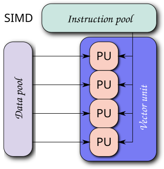
Single instruction, multiple data (SIMD) is a type of parallel processing in Flynn's taxonomy. SIMD can be internal and it can be directly accessible through an instruction set architecture (ISA), but it should not be confused with an ISA. SIMD describes computers with multiple processing elements that perform the same operation on multiple data points simultaneously.

In computing, Streaming SIMD Extensions (SSE) is a single instruction, multiple data (SIMD) instruction set extension to the x86 architecture, designed by Intel and introduced in 1999 in their Pentium III series of central processing units (CPUs) shortly after the appearance of Advanced Micro Devices (AMD's) 3DNow!. SSE contains 70 new instructions, most of which work on single precision floating-point data. SIMD instructions can greatly increase performance when exactly the same operations are to be performed on multiple data objects. Typical applications are digital signal processing and graphics processing.

Visual Instruction Set, or VIS, is a SIMD instruction set extension for SPARC V9 microprocessors developed by Sun Microsystems. There are five versions of VIS: VIS 1, VIS 2, VIS 2+, VIS 3 and VIS 4.

3DNow! is a deprecated extension to the x86 instruction set developed by Advanced Micro Devices (AMD). It adds single instruction multiple data (SIMD) instructions to the base x86 instruction set, enabling it to perform vector processing of floating-point vector operations using vector registers. This improvement enhances the performance of many graphics-intensive applications. The first microprocessor to implement 3DNow! was the AMD K6-2, introduced in 1998. In appropriate applications, this enhancement raised the speed by about 2–4 times.

x86 assembly language is the name for the family of assembly languages which provide some level of backward compatibility with CPUs back to the Intel 8008 microprocessor, which was launched in April 1972. It is used to produce object code for the x86 class of processors.

<span class="mw-page-title-main">AMD K6-2</span> CPU by AMD

The K6-2 is an x86 microprocessor introduced by AMD on May 28, 1998, and available in speeds ranging from 266 to 550 MHz. An enhancement of the original K6, the K6-2 introduced AMD's 3DNow! SIMD instruction set and an upgraded system-bus interface called Super Socket 7, which was backward compatible with older Socket 7 motherboards. It was manufactured using a 250 nanometer process, ran at 2.2 volts, and had 9.3 million transistors.

<span class="mw-page-title-main">AMD K6-III</span> Microprocessor series by AMD

The K6-III was an x86 microprocessor line manufactured by AMD that launched on February 22, 1999. The launch consisted of both 400 and 450 MHz models and was based on the preceding K6-2 architecture. Its improved 256 KB on-chip L2 cache gave it significant improvements in system performance over its predecessor the K6-2. The K6-III was the last processor officially released for desktop Socket 7 systems, however later mobile K6-III+ and K6-2+ processors could be run unofficially in certain socket 7 motherboards if an updated BIOS was made available for a given board. The Pentium III processor from Intel launched 6 days later.

SSE2 is one of the Intel SIMD processor supplementary instruction sets introduced by Intel with the initial version of the Pentium 4 in 2000. SSE2 instructions allow the use of XMM (SIMD) registers on x86 instruction set architecture processors. These registers can load up to 128 bits of data and perform instructions, such as vector addition and multiplication, simultaneously.

SSE3, Streaming SIMD Extensions 3, also known by its Intel code name Prescott New Instructions (PNI), is the third iteration of the SSE instruction set for the IA-32 (x86) architecture. Intel introduced SSE3 in early 2004 with the Prescott revision of their Pentium 4 CPU. In April 2005, AMD introduced a subset of SSE3 in revision E of their Athlon 64 CPUs. The earlier SIMD instruction sets on the x86 platform, from oldest to newest, are MMX, 3DNow!, SSE, and SSE2.

The x86 instruction set refers to the set of instructions that x86-compatible microprocessors support. The instructions are usually part of an executable program, often stored as a computer file and executed on the processor.

A register file is an array of processor registers in a central processing unit (CPU). The instruction set architecture of a CPU will almost always define a set of registers which are used to stage data between memory and the functional units on the chip. The register file is part of the architecture and visible to the programmer, as opposed to the concept of transparent caches. In simpler CPUs, these architectural registers correspond one-for-one to the entries in a physical register file (PRF) within the CPU. More complicated CPUs use register renaming, so that the mapping of which physical entry stores a particular architectural register changes dynamically during execution.

x87 is a floating-point-related subset of the x86 architecture instruction set. It originated as an extension of the 8086 instruction set in the form of optional floating-point coprocessors that work in tandem with corresponding x86 CPUs. These microchips have names ending in "87". This is also known as the NPX. Like other extensions to the basic instruction set, x87 instructions are not strictly needed to construct working programs, but provide hardware and microcode implementations of common numerical tasks, allowing these tasks to be performed much faster than corresponding machine code routines can. The x87 instruction set includes instructions for basic floating-point operations such as addition, subtraction and comparison, but also for more complex numerical operations, such as the computation of the tangent function and its inverse, for example.

Supplemental Streaming SIMD Extensions 3 is a SIMD instruction set created by Intel and is the fourth iteration of the SSE technology.

SSE4 is a SIMD CPU instruction set used in the Intel Core microarchitecture and AMD K10 (K8L). It was announced on September 27, 2006, at the Fall 2006 Intel Developer Forum, with vague details in a white paper; more precise details of 47 instructions became available at the Spring 2007 Intel Developer Forum in Beijing, in the presentation. SSE4 extended the SSE3 instruction set which was released in early 2004. All software using previous Intel SIMD instructions are compatible with modern microprocessors supporting SSE4 instructions. All existing software continues to run correctly without modification on microprocessors that incorporate SSE4, as well as in the presence of existing and new applications that incorporate SSE4.

Advanced Vector Extensions are SIMD extensions to the x86 instruction set architecture for microprocessors from Intel and Advanced Micro Devices (AMD). They were proposed by Intel in March 2008 and first supported by Intel with the Sandy Bridge processor shipping in Q1 2011 and later by AMD with the Bulldozer processor shipping in Q3 2011. AVX provides new features, new instructions, and a new coding scheme.

The VEX prefix and VEX coding scheme are an extension to the IA-32 and x86-64 instruction set architecture for microprocessors from Intel, AMD and others.

References

  1. 1 2 "Makers Unveil PCs With Intel's MMX Chip". The New York Times . January 9, 1997. Archived from the original on January 13, 2019. Retrieved January 13, 2019. Intel's new multimedia extension technology, called MMX, ...
  2. Ch, Rajiv; rasekaran (January 8, 1997). "Intel to unveil faster Pentium chip". The Washington Post . Archived from the original on January 14, 2019. Retrieved January 13, 2019.
  3. "Embedded Pentium Processors with MMX Technology". Intel. Archived from the original on August 11, 2010. Retrieved July 28, 2007.
  4. Mittal, Millind; Peleg, Alex; Weiser, Uri (1997). "MMX Technology Architecture Overview" (PDF). Intel Technology Journal. 1 (3). Archived (PDF) from the original on March 4, 2016. Retrieved October 29, 2015.
  5. 1 2 Calem, Robert E. (January 24, 1997). "Intel's MMX: The Technology Behind the Hoopla". The New York Times. Archived from the original on January 13, 2019. Retrieved January 13, 2019.
  6. Tanaka, Jennifer (February 16, 1997). "A new chip off the block". Newsweek . Archived from the original on August 31, 2019. Retrieved August 31, 2019. the name, which doesn't stand for anything
  7. "Intel | Data Center Solutions, IoT, and PC Innovation". Archived from the original on December 17, 2013. Retrieved December 17, 2013.
  8. Zhang, Peng (January 1, 2010). "CHAPTER 5 - Microprocessors". Advanced Industrial Control Technology. (12) MMX technology: William Andrew Publishing. pp. 155–214. ISBN   978-1-4377-7807-6 . Retrieved June 2, 2024.{{cite book}}: CS1 maint: location (link)
  9. "Intel and Advance Micro agree on chip trademark". The New York Times . April 22, 1997. Archived from the original on January 13, 2019. Retrieved January 13, 2019.
  10. Pfeiffer, Joseph J. Jr. (1997). "MMX Microarchitecture of Pentium Processors With MMX Technology and Pentium II Microprocessors" (PDF). Intel Technology Journal. Archived from the original (PDF) on January 12, 2011. Retrieved September 1, 2017.
  11. 1 2 Conte, G.; Tommesani, S.; Zanichelli, F. (2000). The long and winding road to high-performance image processing with MMX/SSE (PDF). Proceedings of IEEE International Workshop on Computer Architectures for Machine Perception. Archived from the original (PDF) on January 28, 2016.
  12. Kay, Alan S. (February 26, 1999). "Pentium III: Buy the Numbers?". The Washington Post . Archived from the original on April 15, 2019. Retrieved January 13, 2019.
  13. "Microprocessor Hall of Fame". Intel Museum. Archived from the original on April 6, 2008.
  14. "Intel Brings MMX™ Technology To Intel® Personal Internet Client Architecture-Based Wireless Devices" . Retrieved July 28, 2022.
  15. "Intel Delivers Next-Generation Processors Specifically Designed For Cell Phones And Wireless PDAs". Archived from the original on January 2, 2012. Retrieved July 28, 2022.
  16. "World's smallest PXA270 embedded CPU card?". EE Times . September 15, 2004. Retrieved July 28, 2022.