Semiconductor device fabrication |
---|
MOSFET scaling (process nodes) |
Future
|
In semiconductor fabrication, the International Technology Roadmap for Semiconductors (ITRS) defines the "10 nanometer process" as the MOSFET technology node following the "14 nm" node.
Since at least 1997, "process nodes" have been named purely on a marketing basis, and have no relation to the dimensions on the integrated circuit; [1] neither gate length, metal pitch or gate pitch on a "10nm" device is ten nanometers. [2] [3] [4] For example, GlobalFoundries' "7 nm" processes are dimensionally similar to Intel's "10 nm" process. [5] TSMC and Samsung's "10 nm" processes are somewhere between Intel's "14 nm" and "10 nm" processes in transistor density. The transistor density (number of transistors per square millimetre) is more important than transistor size, since smaller transistors no longer necessarily mean improved performance, or an increase in the number of transistors.[ citation needed ]
All production "10 nm" processes are based on FinFET (fin field-effect transistor) technology, a type of multi-gate MOSFET technology that is a non-planar evolution of planar silicon CMOS technology. Samsung first started their production of "10 nm-class" chips in 2013 for their multi-level cell (MLC) flash memory chips, followed by their SoCs using their 10 nm process in 2016. TSMC began commercial production of "10 nm" chips in 2016, and Intel later began production of "10 nm" chips in 2018.[ needs update ]
The ITRS's original naming of this technology node was "11 nm". According to the 2007 edition of the roadmap, by the year 2022, the half-pitch (i.e., half the distance between identical features in an array) for a DRAM was projected to be 11 nm.
In 2008, Pat Gelsinger, at the time serving as Intel's Chief Technology Officer, said that Intel saw a 'clear way' towards the "10 nm" node. [6] [7]
In 2011, Samsung announced plans to introduce the "10 nm" process the following year. [8] [ needs update ] In 2012, Samsung announced eMMC flash memory chips that are produced using the "10 nm" process. [9]
As of 2018, "10 nm" as it was generally understood was only in high-volume production at Samsung. GlobalFoundries had skipped "10 nm",[ needs update ] Intel had not yet started high-volume "10 nm" production, due to yield issues,[ needs update ] and TSMC had considered "10 nm" to be a short-lived node, [10] mainly dedicated to processors for Apple during 2017–2018, moving on to "7 nm" in 2018.[ needs update ]
There is also a distinction to be made between "10 nm" as marketed by foundries and "10 nm" as marketed by DRAM companies.
In April 2013, Samsung announced that it had begun mass production of multi-level cell (MLC) flash memory chips using a "10 nm-class" process, which, according to Tom's Hardware, Samsung defined as "a process technology node somewhere between 10-nm and 20-nm". [11] On 17 October 2016, Samsung Electronics announced mass production of SoC chips at "10 nm". [12] The technology's main announced challenge at that time had been triple patterning for its metal layer. [13] [14] [ needs update ]
TSMC began commercial production of "10 nm" chips in early 2016, before moving onto mass production in early 2017. [15]
On 21 April 2017, Samsung started shipping their Galaxy S8 smartphone, which used the company's version of the "10 nm" processor. [16] [ needs update ] On 12 June 2017, Apple delivered second-generation iPad Pro tablets powered with TSMC-produced Apple A10X chips using the "10 nm" FinFET process. [17]
On 12 September 2017, Apple announced the Apple A11, a 64-bit ARM-based system on a chip, manufactured by TSMC using a "10 nm" FinFET process, containing 4.3 billion transistors on a die of 87.66 mm2.
In April 2018, Intel announced a delay in volume production of "10 nm" mainstream CPUs until sometime in 2019. [18] In July, the exact time was further pinned down to the holiday season. [19] In the meantime, however, they did release a low-power "10 nm" mobile chip, albeit exclusive to Chinese markets and with much of the chip disabled. [20] [ needs update ]
In June 2018 at VLSI 2018, Samsung announced their "11LPP" and "8LPP" processes. "11LPP" was a hybrid based on Samsung "14 nm" and "10 nm" technology. "11LPP" was based on their "10 nm" BEOL, not their "20 nm" BEOL like the "14LPP". "8LPP" was based on the "10LPP" process. [21] [22] [ needs update ]
Nvidia released their GeForce 30 series GPUs in September 2020. They were at that time made on a custom version of Samsung's "8 nm" process, called "Samsung 8N", with a transistor density of 44.56 million transistors per mm2. [23] [24] [ needs update ]
ITRS Logic Device Ground Rules (2015) | Samsung | TSMC | Intel | |||||||
---|---|---|---|---|---|---|---|---|---|---|
Process name | 16/14 nm | 11/10 nm | 10LPE (10 nm) | 10LPP (10 nm) | 8LPP (8 nm) | 8LPU (8 nm) | 8LPA (8 nm) | 10FF (10 nm) | 10nm [25] | 10nm SF (10 nm) [lower-alpha 1] |
Transistor density (MTr / mm2) | Unknown | Unknown | 51.82 [22] | 61.18 [22] | Unknown | 52.51 [27] | 100.76 [28] [lower-alpha 2] | |||
Transistor gate pitch (nm) | 70 | 48 | 68 | 64 | Unknown | 66 | 54 | |||
Interconnect pitch (nm) | 56 | 36 | 51 | Unknown | Unknown | 44 | 36 | |||
Transistor fin pitch (nm) | 42 | 36 | 42 | Unknown | 36 | 34 | ||||
Transistor fin height (nm) | 42 | 42 | 49 | Unknown | Unknown | 42 | 53 | |||
Production year | 2015 | 2017 | 2016 Q4 production [30] | 2017 Q4 production [31] | 2018 production | 2018 risk production 2019 production [32] | 2021 production | 2016 risk production [15] 2017 production [15] | 2018 production (Cannon Lake) [33] | 2020 production (Tiger Lake) [34] |
Transistor gate pitch is also referred to as CPP (contacted poly pitch) and interconnect pitch is also referred to as MMP (minimum metal pitch). Samsung reported their "10 nm" process as having a 64 nm transistor gate pitch and 48 nm interconnect pitch. TSMC reported their "10 nm" process as having a 64 nm transistor gate pitch and 42 nm interconnect pitch. Further investigation by Tech Insights revealed even these values to also be false, and they have been updated accordingly. In addition, the transistor fin height of Samsung's "10 nm" process was updated by MSSCORPS CO at SEMICON Taiwan 2017. [35] [36] [37] [38] [39] GlobalFoundries decided not to develop a "10 nm" node, because it believed it would be short lived. [40] Samsung's "8 nm" process was at that time the company's last to exclusively use DUV lithography. [41] [ needs update ]
For the DRAM industry, the term "10 nm-class" is often used and this dimension generally refers to the half-pitch of the active area.[ citation needed ] The "10 nm" foundry structures are generally much larger.[ citation needed ]
Generally "10 nm class" refers to DRAM with a 10-19 nm feature size, and was first introduced c. 2016. As of 2020, there were three generations of "10 nm class" DRAM : 1x nm (19-17 nm, Gen1); 1y nm (16-14 nm, Gen2); and 1z nm (13-11 nm, Gen3). [42] 3rd Generation "1z" DRAM was first introduced c. 2019 by Samsung, and was initially stated to be produced using ArF lithography without the use of EUV lithography; [43] [44] subsequent production did utilise EUV lithography. [45]
Beyond 1z Samsung named its next node (fourth generation "10 nm class") DRAM : "D1a" (expected at that time to have been produced in 2021), and beyond that "D1b" (expected at that time to have been produced in 2022)[ needs update ]; whilst Micron referred[ needs update ] to succeeding "nodes" as "D1α" and "D1β". [46] Micron announced volume shipment of 1α class DRAM in early 2021. [47]
Semiconductor device fabrication is the process used to manufacture semiconductor devices, typically integrated circuits (ICs) such as computer processors, microcontrollers, and memory chips. It is a multiple-step photolithographic and physico-chemical process during which electronic circuits are gradually created on a wafer, typically made of pure single-crystal semiconducting material. Silicon is almost always used, but various compound semiconductors are used for specialized applications.
Moore's law is the observation that the number of transistors in an integrated circuit (IC) doubles about every two years. Moore's law is an observation and projection of a historical trend. Rather than a law of physics, it is an empirical relationship. It is an experience-curve law, a type of law quantifying efficiency gains from experience in production.
Taiwan Semiconductor Manufacturing Company Limited is a Taiwanese multinational semiconductor contract manufacturing and design company. It is the world's second-most valuable semiconductor company, the world's largest dedicated independent ("pure-play") semiconductor foundry, and its country's largest company, with headquarters and main operations located in the Hsinchu Science Park in Hsinchu, Taiwan. Although the central government of Taiwan is the largest individual shareholder, the majority of TSMC is owned by foreign investors. In 2023, the company was ranked 44th in the Forbes Global 2000.
The 90 nm process refers to the technology used in semiconductor manufacturing to create integrated circuits with a minimum feature size of 90 nanometers. It was an advancement over the previous 130 nm process. Eventually, it was succeeded by smaller process nodes, such as the 65 nm, 45 nm, and 32 nm processes.
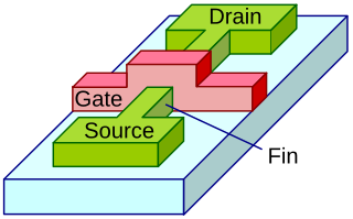
A fin field-effect transistor (FinFET) is a multigate device, a MOSFET built on a substrate where the gate is placed on two, three, or four sides of the channel or wrapped around the channel, forming a double or even multi gate structure. These devices have been given the generic name "FinFETs" because the source/drain region forms fins on the silicon surface. The FinFET devices have significantly faster switching times and higher current density than planar CMOS technology.
The "32 nm" node is the step following the "45 nm" process in CMOS (MOSFET) semiconductor device fabrication. "32-nanometre" refers to the average half-pitch of a memory cell at this technology level.
The transistor count is the number of transistors in an electronic device. It is the most common measure of integrated circuit complexity. The rate at which MOS transistor counts have increased generally follows Moore's law, which observes that transistor count doubles approximately every two years. However, being directly proportional to the area of a die, transistor count does not represent how advanced the corresponding manufacturing technology is. A better indication of this is transistor density which is the ratio of a semiconductor's transistor count to its die area.
The "22 nm" node is the process step following 32 nm in CMOS MOSFET semiconductor device fabrication. The typical half-pitch for a memory cell using the process is around 22 nm. It was first demonstrated by semiconductor companies for use in RAM memory in 2008. In 2010, Toshiba began shipping 24 nm flash memory chips, and Samsung Electronics began mass-producing 20 nm flash memory chips. The first consumer-level CPU deliveries using a 22 nm process started in April 2012 with the Intel Ivy Bridge processors.
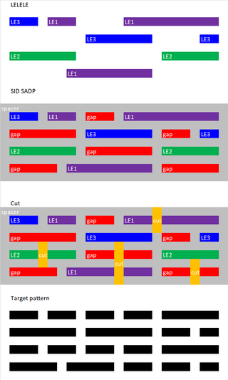
Multiple patterning is a class of technologies for manufacturing integrated circuits (ICs), developed for photolithography to enhance the feature density. It is expected to be necessary for the 10 nm and 7 nm node semiconductor processes and beyond. The premise is that a single lithographic exposure may not be enough to provide sufficient resolution. Hence additional exposures would be needed, or else positioning patterns using etched feature sidewalls would be necessary.
The "14 nanometer process" refers to a marketing term for the MOSFET technology node that is the successor to the "22 nm" node. The "14 nm" was so named by the International Technology Roadmap for Semiconductors (ITRS). Until about 2011, the node following "22 nm" was expected to be "16 nm". All "14 nm" nodes use FinFET technology, a type of multi-gate MOSFET technology that is a non-planar evolution of planar silicon CMOS technology.
A multigate device, multi-gate MOSFET or multi-gate field-effect transistor (MuGFET) refers to a metal–oxide–semiconductor field-effect transistor (MOSFET) that has more than one gate on a single transistor. The multiple gates may be controlled by a single gate electrode, wherein the multiple gate surfaces act electrically as a single gate, or by independent gate electrodes. A multigate device employing independent gate electrodes is sometimes called a multiple-independent-gate field-effect transistor (MIGFET). The most widely used multi-gate devices are the FinFET and the GAAFET, which are non-planar transistors, or 3D transistors.
GlobalFoundries Inc. is a multinational semiconductor contract manufacturing and design company incorporated in the Cayman Islands and headquartered in Malta, New York. Created by the divestiture of the manufacturing arm of AMD, the company was privately owned by Mubadala Investment Company, a sovereign wealth fund of the United Arab Emirates, until an initial public offering (IPO) in October 2021.
Per the International Technology Roadmap for Semiconductors, the 45 nm process is a MOSFET technology node referring to the average half-pitch of a memory cell manufactured at around the 2007–2008 time frame.
In semiconductor manufacturing, the International Roadmap for Devices and Systems defines the "5 nm" process as the MOSFET technology node following the "7 nm" node. In 2020, Samsung and TSMC entered volume production of "5 nm" chips, manufactured for companies including Apple, Marvell, Huawei and Qualcomm.
In semiconductor manufacturing, the "7 nm" process is a term for the MOSFET technology node following the "10 nm" node, defined by the International Roadmap for Devices and Systems (IRDS), which was preceded by the International Technology Roadmap for Semiconductors (ITRS). It is based on FinFET technology, a type of multi-gate MOSFET technology.
Dr. Gary Patton is an American technologist and business executive. He is currently the Corporate Vice President and General Manager of Design Enablement and Components Research in the Technology Development Group at Intel. He has spent most of his career in IBM, starting in IBM's Research Division and holding management and executive positions in IBM's Microelectronics Division in Technology Development, Design Enablement, Manufacturing, and Business Line Management.
In semiconductor manufacturing, the 3nm process is the next die shrink after the 5 nm MOSFET technology node. South Korean chipmaker Samsung started shipping its 3 nm gate all around (GAA) process, named 3GAA, in mid-2022. On 29 December 2022, Taiwanese chip manufacturer TSMC announced that volume production using its 3 nm semiconductor node (N3) was under way with good yields. An enhanced 3 nm chip process called "N3E" may have started production in 2023. American manufacturer Intel planned to start 3 nm production in 2023.
In semiconductor manufacturing, the "2 nm process" is the next MOSFET die shrink after the "3 nm" process node.
The "28 nm" lithography process is a half-node semiconductor manufacturing process based on a die shrink of the "32 nm" lithography process. It appeared in production in 2010.
Samsung 10LPE process
Preceded by 14 nm | MOSFET manufacturing processes | Succeeded by 7 nm |