WO2019130963A1 - Solid-state imaging element, comparator, and electronic device - Google Patents
Solid-state imaging element, comparator, and electronic device Download PDFInfo
- Publication number
- WO2019130963A1 WO2019130963A1 PCT/JP2018/043770 JP2018043770W WO2019130963A1 WO 2019130963 A1 WO2019130963 A1 WO 2019130963A1 JP 2018043770 W JP2018043770 W JP 2018043770W WO 2019130963 A1 WO2019130963 A1 WO 2019130963A1
- Authority
- WO
- WIPO (PCT)
- Prior art keywords
- unit
- active load
- transistor
- analog
- solid
- Prior art date
Links
- 238000003384 imaging method Methods 0.000 title claims abstract description 105
- 238000006243 chemical reaction Methods 0.000 claims abstract description 41
- 239000011159 matrix material Substances 0.000 claims abstract description 11
- 230000005669 field effect Effects 0.000 claims description 78
- 238000001514 detection method Methods 0.000 description 47
- 238000004891 communication Methods 0.000 description 44
- 238000012545 processing Methods 0.000 description 35
- 238000000034 method Methods 0.000 description 27
- 239000004065 semiconductor Substances 0.000 description 25
- 238000012546 transfer Methods 0.000 description 25
- 238000005516 engineering process Methods 0.000 description 24
- 238000010586 diagram Methods 0.000 description 22
- 230000008569 process Effects 0.000 description 20
- 239000000758 substrate Substances 0.000 description 20
- 230000004048 modification Effects 0.000 description 19
- 238000012986 modification Methods 0.000 description 19
- 230000003321 amplification Effects 0.000 description 15
- 238000003199 nucleic acid amplification method Methods 0.000 description 15
- 230000006870 function Effects 0.000 description 14
- 239000010410 layer Substances 0.000 description 14
- 238000009792 diffusion process Methods 0.000 description 10
- 230000000694 effects Effects 0.000 description 10
- 238000007667 floating Methods 0.000 description 10
- 238000003860 storage Methods 0.000 description 9
- 239000002184 metal Substances 0.000 description 8
- 230000007274 generation of a signal involved in cell-cell signaling Effects 0.000 description 6
- 230000002093 peripheral effect Effects 0.000 description 6
- 230000009467 reduction Effects 0.000 description 6
- 238000004519 manufacturing process Methods 0.000 description 5
- 230000007246 mechanism Effects 0.000 description 5
- 230000003287 optical effect Effects 0.000 description 5
- 238000010408 sweeping Methods 0.000 description 5
- 239000003990 capacitor Substances 0.000 description 4
- 230000006872 improvement Effects 0.000 description 4
- 239000007769 metal material Substances 0.000 description 4
- 230000004044 response Effects 0.000 description 4
- 230000008859 change Effects 0.000 description 3
- 238000012544 monitoring process Methods 0.000 description 3
- 230000002123 temporal effect Effects 0.000 description 3
- 230000001133 acceleration Effects 0.000 description 2
- 230000005540 biological transmission Effects 0.000 description 2
- 230000015572 biosynthetic process Effects 0.000 description 2
- 230000010267 cellular communication Effects 0.000 description 2
- 238000002485 combustion reaction Methods 0.000 description 2
- 230000000295 complement effect Effects 0.000 description 2
- 238000012937 correction Methods 0.000 description 2
- 230000007423 decrease Effects 0.000 description 2
- 238000013461 design Methods 0.000 description 2
- 238000009826 distribution Methods 0.000 description 2
- 238000005401 electroluminescence Methods 0.000 description 2
- 238000009434 installation Methods 0.000 description 2
- 229910044991 metal oxide Inorganic materials 0.000 description 2
- 150000004706 metal oxides Chemical class 0.000 description 2
- 229910021420 polycrystalline silicon Inorganic materials 0.000 description 2
- 229920005591 polysilicon Polymers 0.000 description 2
- 230000005236 sound signal Effects 0.000 description 2
- 238000001228 spectrum Methods 0.000 description 2
- 240000004050 Pentaglottis sempervirens Species 0.000 description 1
- 235000004522 Pentaglottis sempervirens Nutrition 0.000 description 1
- XUIMIQQOPSSXEZ-UHFFFAOYSA-N Silicon Chemical compound [Si] XUIMIQQOPSSXEZ-UHFFFAOYSA-N 0.000 description 1
- 238000009825 accumulation Methods 0.000 description 1
- 230000009471 action Effects 0.000 description 1
- 230000003190 augmentative effect Effects 0.000 description 1
- 230000003796 beauty Effects 0.000 description 1
- 230000008901 benefit Effects 0.000 description 1
- 210000004204 blood vessel Anatomy 0.000 description 1
- 238000004364 calculation method Methods 0.000 description 1
- 230000001413 cellular effect Effects 0.000 description 1
- 238000010276 construction Methods 0.000 description 1
- 238000001816 cooling Methods 0.000 description 1
- 238000007306 functionalization reaction Methods 0.000 description 1
- 230000005484 gravity Effects 0.000 description 1
- 210000003128 head Anatomy 0.000 description 1
- 239000012535 impurity Substances 0.000 description 1
- 230000010354 integration Effects 0.000 description 1
- 239000011229 interlayer Substances 0.000 description 1
- 238000002955 isolation Methods 0.000 description 1
- 239000004973 liquid crystal related substance Substances 0.000 description 1
- 230000007774 longterm Effects 0.000 description 1
- 238000012423 maintenance Methods 0.000 description 1
- 239000000463 material Substances 0.000 description 1
- 230000000116 mitigating effect Effects 0.000 description 1
- 238000010295 mobile communication Methods 0.000 description 1
- 239000002245 particle Substances 0.000 description 1
- 238000005498 polishing Methods 0.000 description 1
- 230000002265 prevention Effects 0.000 description 1
- 210000004761 scalp Anatomy 0.000 description 1
- 230000035939 shock Effects 0.000 description 1
- 229910052710 silicon Inorganic materials 0.000 description 1
- 239000010703 silicon Substances 0.000 description 1
- 238000005549 size reduction Methods 0.000 description 1
- 239000000126 substance Substances 0.000 description 1
Images


Classifications
-
- H01L27/14609—
-
- H—ELECTRICITY
- H04—ELECTRIC COMMUNICATION TECHNIQUE
- H04M—TELEPHONIC COMMUNICATION
- H04M1/00—Substation equipment, e.g. for use by subscribers
- H04M1/02—Constructional features of telephone sets
- H04M1/0202—Portable telephone sets, e.g. cordless phones, mobile phones or bar type handsets
- H04M1/026—Details of the structure or mounting of specific components
- H04M1/0264—Details of the structure or mounting of specific components for a camera module assembly
-
- H—ELECTRICITY
- H04—ELECTRIC COMMUNICATION TECHNIQUE
- H04N—PICTORIAL COMMUNICATION, e.g. TELEVISION
- H04N25/00—Circuitry of solid-state image sensors [SSIS]; Control thereof
- H04N25/70—SSIS architectures; Circuits associated therewith
- H04N25/71—Charge-coupled device [CCD] sensors; Charge-transfer registers specially adapted for CCD sensors
- H04N25/75—Circuitry for providing, modifying or processing image signals from the pixel array
-
- H01L27/14605—
-
- H01L27/14612—
-
- H01L27/14625—
-
- H01L27/14643—
-
- H—ELECTRICITY
- H04—ELECTRIC COMMUNICATION TECHNIQUE
- H04M—TELEPHONIC COMMUNICATION
- H04M1/00—Substation equipment, e.g. for use by subscribers
- H04M1/02—Constructional features of telephone sets
-
- H—ELECTRICITY
- H04—ELECTRIC COMMUNICATION TECHNIQUE
- H04N—PICTORIAL COMMUNICATION, e.g. TELEVISION
- H04N23/00—Cameras or camera modules comprising electronic image sensors; Control thereof
- H04N23/50—Constructional details
- H04N23/55—Optical parts specially adapted for electronic image sensors; Mounting thereof
-
- H—ELECTRICITY
- H04—ELECTRIC COMMUNICATION TECHNIQUE
- H04N—PICTORIAL COMMUNICATION, e.g. TELEVISION
- H04N23/00—Cameras or camera modules comprising electronic image sensors; Control thereof
- H04N23/57—Mechanical or electrical details of cameras or camera modules specially adapted for being embedded in other devices
-
- H—ELECTRICITY
- H04—ELECTRIC COMMUNICATION TECHNIQUE
- H04N—PICTORIAL COMMUNICATION, e.g. TELEVISION
- H04N23/00—Cameras or camera modules comprising electronic image sensors; Control thereof
- H04N23/95—Computational photography systems, e.g. light-field imaging systems
-
- H—ELECTRICITY
- H04—ELECTRIC COMMUNICATION TECHNIQUE
- H04N—PICTORIAL COMMUNICATION, e.g. TELEVISION
- H04N25/00—Circuitry of solid-state image sensors [SSIS]; Control thereof
- H04N25/60—Noise processing, e.g. detecting, correcting, reducing or removing noise
-
- H—ELECTRICITY
- H04—ELECTRIC COMMUNICATION TECHNIQUE
- H04N—PICTORIAL COMMUNICATION, e.g. TELEVISION
- H04N25/00—Circuitry of solid-state image sensors [SSIS]; Control thereof
- H04N25/60—Noise processing, e.g. detecting, correcting, reducing or removing noise
- H04N25/67—Noise processing, e.g. detecting, correcting, reducing or removing noise applied to fixed-pattern noise, e.g. non-uniformity of response
-
- H—ELECTRICITY
- H04—ELECTRIC COMMUNICATION TECHNIQUE
- H04N—PICTORIAL COMMUNICATION, e.g. TELEVISION
- H04N25/00—Circuitry of solid-state image sensors [SSIS]; Control thereof
- H04N25/70—SSIS architectures; Circuits associated therewith
- H04N25/76—Addressed sensors, e.g. MOS or CMOS sensors
-
- H—ELECTRICITY
- H04—ELECTRIC COMMUNICATION TECHNIQUE
- H04N—PICTORIAL COMMUNICATION, e.g. TELEVISION
- H04N25/00—Circuitry of solid-state image sensors [SSIS]; Control thereof
- H04N25/70—SSIS architectures; Circuits associated therewith
- H04N25/76—Addressed sensors, e.g. MOS or CMOS sensors
- H04N25/78—Readout circuits for addressed sensors, e.g. output amplifiers or A/D converters
Definitions
- the present disclosure relates to a solid-state imaging device, a comparator, and an electronic device.
- CMOS image sensors that can be manufactured using existing CMOS processes have attracted attention without requiring special equipment investment, and their adoption in camera systems and surveillance systems built into mobile phones is rapidly advancing. It is.
- a CMOS image sensor converts an analog pixel signal (electric signal) output by a unit pixel (hereinafter, may be simply described as “pixel”) that performs photoelectric conversion into a digital signal (AD (Analog to Digital) conversion)
- pixel an analog-digital conversion unit of a CMOS image sensor
- AD Analog to Digital
- a column parallel type analog-to-digital converter (hereinafter sometimes referred to as a column parallel analog-to-digital converter) that can be converted is adopted.
- the column parallel analog-to-digital converter is configured, for example, by arranging a plurality of analog-to-digital converters (AD converters), such as the same number as the number of columns of pixel columns, in the row direction. Then, the analog-to-digital converter of each column performs analog-to-digital conversion of the electrical signal output from the unit pixel of the corresponding pixel column.
- the analog-to-digital converter constituting the column parallel analog-to-digital converter includes, for example, a comparator and a counter, and compares pixels with a predetermined reference signal and an analog pixel signal output from a unit pixel. There is a so-called reference signal comparison type analog-to-digital converter that performs analog-to-digital conversion of signals.
- a single slope type analog-to-digital converter As a reference signal comparison type analog-to-digital converter, a single slope type analog-to-digital converter is known (see, for example, Patent Document 1).
- a single slope type analog-to-digital converter for example, in a comparator composed of a differential input unit composed of field effect transistors and an active load unit of the differential input unit, the level is set at a constant slope of a ramp (RAMP) signal or the like.
- RAMP ramp
- a comparison is made between the changing reference signal and the pixel signal output by the unit pixel. Then, the counter counts the time required for the change in the level of the reference signal until the levels of the reference signal and the pixel signal match.
- analog-digital conversion of an analog pixel signal (electric signal) output from the unit pixel is performed.
- the noise power of this random noise is inversely proportional to the area of the control terminal of the transistor that constitutes the comparator. That is, when the area of the control terminal of the transistor is large, the noise power of random noise can be reduced.
- increasing the area of the control terminal of the transistor leads to an increase in the circuit area of the comparator.
- a solid-state imaging device for achieving the above object is: A pixel array unit in which a plurality of unit pixels including a photoelectric conversion unit are arranged in a matrix, and an analog-digital conversion unit converting an analog pixel signal output from each unit pixel of the pixel array unit into a digital signal ,
- the analog-to-digital conversion unit has a comparator including a differential input unit to which a predetermined reference signal and an analog pixel signal are input and an active load unit of the differential input unit.
- At least one transistor constituting the active load has a plurality of control terminals for controlling the current, The plurality of control terminals are electrically connected in common.
- the comparator of the present disclosure for achieving the above object is Including a differential input receiving a predetermined reference signal and an analog pixel signal and an active load of the differential input; At least one transistor constituting the active load has a plurality of control terminals for controlling the current, The plurality of control terminals are electrically connected in common.
- An electronic device of the present disclosure for achieving the above object has a solid-state imaging device of the above configuration.
- FIG. 1 is a block diagram schematically showing the basic configuration of the CMOS image sensor of the present disclosure.
- FIG. 2 is a circuit diagram showing an example of a circuit configuration of a unit pixel.
- FIG. 3 is a block diagram showing an example of the configuration of the column parallel analog-to-digital converter.
- FIG. 4 is a plan view schematically showing a flat type chip structure of the CMOS image sensor of the present disclosure.
- FIG. 5 is an exploded perspective view showing an outline of the stacked chip structure of the CMOS image sensor of the present disclosure.
- FIG. 6A is a circuit diagram showing an example of a circuit configuration of a comparator composed of field effect transistors
- FIG. 6B is a plan view showing a layout of a multi-finger structure.
- FIG. 7A is a plan view showing the layout of the main part of the active load unit according to the first embodiment
- FIG. 7B is a plan view showing the layout of a multi-finger structure according to a reference example.
- FIG. 8 is a cross-sectional view showing a cross section taken along line AA of FIG. 7A.
- Figure 9 is a diagram showing a mutual conductance gm with respect to the drain current I d when the four PMOS transistors, manufactured in the layout of the layout as in Reference Example in Example 1.
- Figure 10 is a random noise spectrum of the transistor itself which constitutes the active load unit is a diagram showing the gate input referred noise SV g.
- FIG. 11 is a diagram comparing the case of using the layout of the first embodiment with the case of using the layout of the reference example with regard to the improvement effect of the random noise and the output voltage variation of the comparator.
- 12A is a plan view showing the layout of the main part of the active load unit according to the second embodiment
- FIG. 12B is a layout view showing an example of the common centroid arrangement.
- FIG. 13 is a plan view showing the layout of the main part of the active load unit according to the third embodiment.
- FIG. 14 is a plan view showing the layout of the main part of the active load unit according to the third embodiment.
- FIG. 15 is a plan view showing the layout of the main part of the active load unit according to the fourth embodiment.
- FIG. 16 is a plan view showing the layout of the main part of the active load unit according to the sixth embodiment.
- FIG. 17 is a plan view showing the layout of the main part of the active load unit according to the seventh embodiment.
- FIG. 18 is a plan view showing the layout of the main parts of the active load portion according to the eighth embodiment.
- FIG. 19A is a plan view showing the layout of the main part of the active load portion according to Embodiment 9, and FIG. 19B is a cross-sectional view showing the arrow cross section along line BB in FIG. 19A.
- FIG. 20A is a plan view showing the layout of the main part of the active load unit according to the tenth embodiment, and FIG. 20B is a plan view showing the layout of the main part of the active load unit according to the eleventh embodiment.
- FIG. 21A is a plan view showing the layout of the main part of an active load unit according to the twelfth embodiment
- FIG. 21B is a plan view showing the layout of the main part of the active load unit according to the thirteenth embodiment.
- FIG. 22 is a circuit diagram showing an example of a circuit configuration of a comparator composed of bipolar transistors.
- FIG. 23 is a plan view showing the layout of the main parts of the active load portion according to the fourteenth embodiment.
- FIG. 24 is a plan view showing the layout of the main parts of the active load portion according to the fifteenth embodiment.
- FIG. 25 is a plan view showing the layout of the main parts of the active load portion according to the fifteenth embodiment.
- FIG. 22 is a circuit diagram showing an example of a circuit configuration of a comparator composed of bipolar transistors.
- FIG. 23 is a plan view showing the layout of the main parts of the active load portion according to the fourteenth embodiment.
- FIG. 24 is a plan view showing the layout of the main parts of
- FIG. 26A is a circuit diagram showing a circuit example of an analog switch according to Application Example 1
- FIG. 26B is a waveform diagram showing waveforms of a detection signal and an output signal of the analog switch.
- FIG. 27A is a circuit diagram showing an example of a triangular wave generation circuit according to Application Example 2
- FIG. 27B is a waveform diagram showing an output waveform of the triangular wave generation circuit.
- FIG. 28 is a circuit diagram showing a circuit example of a digital-analog converter according to application example 3.
- FIG. 29 is a diagram illustrating an application example of the technology according to the present disclosure.
- FIG. 30 is a block diagram showing a configuration of an imaging device which is an example of the electronic device of the present disclosure.
- FIG. 31 is a block diagram showing a schematic configuration example of a vehicle control system which is an example of a moving object control system to which the technology according to the present disclosure can be applied.
- FIG. 32 is a diagram illustrating an example of the installation position of
- Flat type chip structure (so-called flat structure) 2-4-2. Stacked chip structure (so-called laminated structure) 2-5.
- First embodiment (an example in which a transistor constituting a comparator is a field effect transistor) 2-6-1.
- Example 1 an example in which one of the transistors constituting the active load unit is a field effect transistor) 2-6-2.
- Embodiment 2 (Modification of Embodiment 1: Example of Forming One Field Effect Transistor in One Active Region) 2-6-3.
- Embodiment 3 (Modification of Embodiment 1: Example in which a plurality of field effect transistors are formed in one active region) 2-6-4.
- Second Embodiment an example in which a transistor constituting a comparator is composed of Fin-FET 2-7-1.
- Example 9 an example in which one transistor constituting an active load unit is composed of one Fin-FET 2-7-2.
- Example 10 (example comprising a plurality of Fin-FETs connected in series) 2-7-3.
- Example 11 (example composed of a plurality of Fin-FETs connected in parallel) 2-7-4.
- Example 12 (example in which a series-connected set of Fin-FETs is connected in parallel) 2-7-5.
- Example 13 (example in which a set of parallel-connected Fin-FETs are connected in series) 2-8.
- Example 14 (example in which one bipolar transistor is formed in one active region) 2-8-2.
- Example 15 (example in which a plurality of bipolar transistors are formed in one active region) 2-8-3.
- Example 16 (Modification of Example 15: Example of Series Connection) 3. Application Example of Comparator 3-1.
- Application Example 1 (Example Applied to Analog Switch) 3-2.
- Application example 2 (example applied to a triangular wave generation circuit) 3-3.
- Application Example 3 (Example Applied to Digital-Analog Converter) 4. Modification 5
- Application example 6 Application example of technology according to the present disclosure 6-1.
- Electronic Device of the Present Disclosure (Example of Imaging Device) 6-2.
- At least one transistor that configures the active load unit can be configured to include a plurality of field effect transistors having a plurality of control terminals.
- the drain regions and the source regions of the plurality of field effect transistors may be alternately connected in series, and all gate terminals may be shared.
- a plurality of field effect transistors can be configured to be connected in series through active regions.
- a plurality of field effect transistors can be connected in series through the active region.
- the plurality of field effect transistors can be dispersedly arranged in different active regions, and the different active regions can be connected by a wire.
- a dummy gate terminal is disposed in an active region where a field effect transistor is not formed.
- At least one transistor that configures the active load unit can be configured by a plurality of bipolar transistors having a plurality of control terminals. .
- the emitter regions and the collector regions of the plurality of bipolar transistors can be alternately connected in series, and all the base terminals can be made common.
- the plurality of bipolar transistors are dispersedly disposed in different active regions and connected in series by wiring. can do.
- a plurality of bipolar transistors can be connected in series by wiring between different active regions.
- the plurality of bipolar transistors can be arranged in the same active region, and the base terminals can be shared among the plurality of bipolar transistors.
- At least one transistor that configures the active load unit can be configured to be a Fin-FET.
- CMOS complementary metal oxide semiconductor
- a CMOS image sensor is an image sensor manufactured by applying or partially using a CMOS process.
- FIG. 1 is a block diagram schematically showing the basic configuration of the CMOS image sensor of the present disclosure.
- unit pixels hereinafter may be simply referred to as “pixels”
- pixels unit pixels
- the pixel array unit 11 and a peripheral circuit unit of the pixel array unit 11 are configured.
- the row direction refers to the arrangement direction (the so-called horizontal direction) of the unit pixels 2 in the pixel row
- the column direction refers to the arrangement direction (the so-called vertical direction) the unit pixels 2 in the pixel column.
- the unit pixel 2 performs photoelectric conversion to generate and accumulate photocharges according to the amount of light received.
- the peripheral circuit unit of the pixel array unit 11 includes, for example, a row selection unit 12, a constant current source unit 13, an analog-digital conversion unit 14, a horizontal transfer scanning unit 15, a signal processing unit 16, a timing control unit 17, and the like. It is done.
- pixel drive lines 31 1 to 31 m (hereinafter sometimes collectively referred to as “pixel drive lines 31”) for each pixel row are arranged along the row direction with respect to the pixel array in matrix form. Are wired. Further, vertical signal lines 32 1 to 32 n (hereinafter, sometimes collectively referred to as “vertical signal lines 32”) may be wired along the column direction for each pixel column.
- the pixel drive line 31 transmits a drive signal for driving when reading out a signal from the unit pixel 2.
- FIG. 1 illustrates the pixel drive line 31 as a single wire, it is not limited to one. One end of the pixel drive line 31 is connected to an output end corresponding to each row of the row selection unit 12.
- each circuit unit of the peripheral circuit unit of the pixel array unit 11, that is, the row selection unit 12, the constant current source unit 13, the analog-digital conversion unit 14, the horizontal transfer scanning unit 15, the signal processing unit 16, and the timing The control unit 17 will be described.
- the row selection unit 12 includes a shift register, an address decoder, and the like, and controls the scanning of the pixel row and the address of the pixel row when selecting each pixel 2 of the pixel array unit 11.
- the row selection unit 12 generally has two scanning systems, a reading scanning system and a sweeping scanning system, although its specific configuration is not shown.
- the readout scanning system In order to read out the pixel signal from the unit pixel 2, the readout scanning system sequentially selects and scans the unit pixel 2 of the pixel array unit 11 row by row.
- the pixel signal read out from the unit pixel 2 is an analog signal.
- the sweeping scanning system performs sweeping scanning on the readout row on which readout scanning is performed by the readout scanning system, prior to the readout scanning by the time of the shutter speed.
- Unnecessary charge is swept out from the photoelectric conversion unit of the unit pixel 2 of the readout row by the sweep scanning by the sweep scanning system, and the photoelectric conversion unit is reset. Then, so-called electronic shutter operation is performed by sweeping out (resetting) unnecessary charges by the sweeping scanning system.
- the electronic shutter operation is an operation of discarding the photocharge of the photoelectric conversion unit and newly starting exposure (starting accumulation of photocharge).
- Constant current source unit 13 is formed of a set of current sources I consisting of MOS transistors connected to each of vertical signal lines 32 1 to 32 n for each pixel column (see FIG. 2). A bias current is supplied to each pixel 2 of the pixel row through each of the vertical signal lines 32 1 to 32 n .
- the analog-to-digital converter 14 includes a set of a plurality of analog-to-digital converters provided corresponding to each of the vertical signal lines 32 1 to 32 n , and outputs analog pixel signals output for each pixel column It is a column parallel type analog-to-digital converter that converts an N-bit digital signal.
- a single slope type analog-to-digital converter which is an example of a reference signal comparison type analog-to-digital converter, is used.
- the horizontal transfer scanning unit 15 is configured of a shift register, an address decoder, and the like, and controls the scanning of the pixel column and the address of the pixel column when reading out the signal of each pixel 2 of the pixel array unit 11. Under the control of the horizontal transfer scanning unit 15, pixel signals converted to digital signals by the analog-digital conversion unit 14 are read out to the horizontal transfer line 18 of 2N bit width in units of pixel columns.
- the signal processing unit 16 performs various signal processing such as amplification processing and arithmetic processing on pixel signals supplied through the horizontal transfer line 18 and outputs the processed signal as an output signal of the present CMOS image sensor 1.
- the timing control unit 17 generates various timing signals, clock signals, control signals and the like, and based on the generated signals, the row selection unit 12, the constant current source unit 13, the analog-digital conversion unit 14, the horizontal The drive control of the transfer scanning unit 15 and the signal processing unit 16 is performed.
- FIG. 2 is a circuit diagram showing an example of the circuit configuration of the unit pixel 2.
- the unit pixel 2 includes, for example, a photodiode 21 as a photoelectric conversion unit.
- the unit pixel 2 has a pixel configuration including the transfer transistor 22, the reset transistor 23, the amplification transistor 24, and the selection transistor 25 in addition to the photodiode 21.
- the four transistors of the transfer transistor 22, the reset transistor 23, the amplification transistor 24, and the selection transistor 25, for example, an N-channel MOS type field effect transistor (FET) is used.
- FET field effect transistor
- the combination of the conductivity types of the four transistors 22 to 25 illustrated here is merely an example, and the invention is not limited to the combination.
- a plurality of pixel drive lines are commonly wired to each unit pixel 2 in the same pixel row as the above-described pixel drive line 31 with respect to the unit pixel 2.
- the plurality of pixel drive lines are connected to the output end corresponding to each pixel row of the row selection unit 12 in pixel row units.
- the row selection unit 12 appropriately outputs the transfer signal TRG, the reset signal RST, and the selection signal SEL to a plurality of pixel drive lines.
- the anode terminal of the photodiode 21 is connected to the low potential side power supply (for example, the ground), and the received light is photoelectrically converted into photocharge (here, photoelectrons) having a charge amount corresponding to the light amount. Accumulate charge.
- the cathode terminal of the photodiode 21 is electrically connected to the gate terminal of the amplification transistor 24 via the transfer transistor 22.
- a region where the gate terminals of the amplification transistor 24 are electrically connected is a floating diffusion (floating diffusion region / impurity diffusion region) FD.
- the floating diffusion FD is a charge-voltage converter that converts charge into a voltage.
- a transfer signal TRG whose high level (for example, V DD level) is active is applied to the gate terminal of the transfer transistor 22 from the row selection unit 12.
- the transfer transistor 22 is turned on in response to the transfer signal TRG, and is photoelectrically converted by the photodiode 21 to transfer the light charge accumulated in the photodiode 21 to the floating diffusion FD.
- the reset transistor 23 is connected between the node of the high potential side power supply V DD and the floating diffusion FD.
- a reset signal RST of which the high level is active, is applied from the row selection unit 12 to the gate terminal of the reset transistor 23.
- the reset transistor 23 becomes conductive in response to the reset signal RST, and resets the floating diffusion FD by discarding the charge of the floating diffusion FD to the node of the voltage V DD .
- the gate terminal of the amplification transistor 24 is connected to the floating diffusion FD, and the drain terminal is connected to the node of the high potential side power supply V DD .
- the amplification transistor 24 is an input unit of a source follower that reads a signal obtained by photoelectric conversion in the photodiode 21. That is, the source terminal of the amplification transistor 24 is connected to the vertical signal line 32 via the selection transistor 25.
- the amplification transistor 24 and the current source I connected to one end of the vertical signal line 32 constitute a source follower that converts the voltage of the floating diffusion FD into the potential of the vertical signal line 32.
- the drain terminal of the selection transistor 25 is connected to the source terminal of the amplification transistor 24, and the source terminal is connected to the vertical signal line 32.
- a selection signal SEL whose high level is active is supplied from the row selection unit 12 to the gate terminal of the selection transistor 25.
- the selection transistor 25 becomes conductive in response to the selection signal SEL, and transmits the signal output from the amplification transistor 24 to the vertical signal line 32 with the unit pixel 2 in the selection state.
- the selection transistor 25 may have a circuit configuration connected between the node of the high potential side power supply V DD and the drain terminal of the amplification transistor 24. Further, in this example, as a pixel circuit of the unit pixel 2, a 4Tr configuration including the transfer transistor 22, the reset transistor 23, the amplification transistor 24, and the selection transistor 25; that is, four transistors (Tr) is exemplified. However, it is not limited to this.
- the selection transistor 25 may be omitted, and the amplification transistor 24 may be configured as a 3Tr to have the function of the selection transistor 25. Alternatively, as necessary, the number of transistors may be increased to 5Tr or more. .
- FIG. 3 is a block diagram showing an example of the configuration of the column parallel analog-to-digital converter 14.
- the analog-to-digital converter 14 in the CMOS image sensor 1 of the present disclosure is composed of a set of a plurality of single slope type analog-to-digital converters provided corresponding to each of the vertical signal lines 32 1 to 32 n .
- the n-th column single slope type analog-to-digital converter 140 will be described as an example.
- the single slope type analog-to-digital converter 140 has a circuit configuration including a comparator 141, a counter circuit 142, and a latch circuit 143.
- the single slope analog-to-digital converter 140 uses a reference signal of a so-called RAMP waveform (slope waveform) in which the voltage value gradually changes as time passes.
- the reference signal of the ramp waveform is generated by the reference signal generator 19.
- the reference signal generation unit 19 can be configured, for example, using a DAC (digital-to-analog conversion) circuit.
- the comparator 141 uses a pixel signal read from the unit pixel 2 as a comparison input, uses a reference signal generated by the reference signal generation unit 19 as a reference input, and compares both signals. Then, for example, when the reference signal is higher than the pixel signal, the output of the comparator 141 is in the first state (for example, high level), and when the reference signal is lower than the pixel signal, the output is in the second state (for example, , Low level). Thus, the output signal of the comparator 141 becomes a pulse signal having a pulse width corresponding to the magnitude of the level of the pixel signal.
- the clock signal CLK is supplied from the timing control unit 17 to the counter circuit 142 at the same timing as the supply start timing of the reference signal to the comparator 141. Then, the counter circuit 142 counts the period in synchronization with the clock signal CLK, thereby measuring the period of the pulse width of the output pulse of the comparator 141, that is, the period from the start of the comparison operation to the end of the comparison operation.
- the count result (count value) of the counter circuit 142 is a digital value obtained by digitizing an analog pixel signal.
- the latch circuit 143 latches the digital value which is the count result of the counter circuit 142. Then, under driving by the horizontal transfer scanning unit 15, the latched digital value is output to the horizontal transfer line 18.
- the reference signal of the gradually changing analog value generated by the reference signal generator 19 and the unit A digital value is obtained from time information until the magnitude relation with the analog pixel signal output from the pixel 2 changes.
- the analog-to-digital converter 14 in which the analog-to-digital converter 140 is arranged in a one-to-one relationship with the pixel column is illustrated. It is also possible to use the analog-to-digital converter 14 in which the converter 140 is disposed.
- Chip structure As a chip (semiconductor integrated circuit) structure of the CMOS image sensor 1 of the present disclosure configured as described above, a flat-type chip structure and a stack-type chip structure can be exemplified.
- CMOS image sensor 1 of flat type chip structure and stack type chip structure when the substrate surface on the side on which the wiring layer is arranged is the front surface (front surface) for the unit pixel 2, the back surface on the opposite side A back-illuminated pixel structure can be provided which takes in light emitted from the side.
- the flat type chip structure and the stack type chip structure will be described below.
- FIG. 4 is a plan view schematically showing a flat type chip structure of the CMOS image sensor 1 of the present disclosure.
- the periphery of the pixel array 11 is formed on the same semiconductor substrate 41 as the pixel array 11 in which the unit pixels 2 are arranged in a matrix. It has a structure in which a circuit portion is formed.
- the row selection unit 12, the constant current source unit 13, the analog-digital conversion unit 14, the horizontal transfer scanning unit 15, the signal processing unit 16, and the timing control unit 17 A reference signal generation unit 19, a DC supply unit 20 and the like are formed.
- FIG. 5 is an exploded perspective view showing an outline of the stacked chip structure of the CMOS image sensor of the present disclosure.
- the stacked chip structure so-called stacked structure, has a structure in which at least two semiconductor substrates of the first semiconductor substrate 42 and the second semiconductor substrate 43 are stacked.
- the pixel array unit 11 is formed on the first semiconductor substrate 42 of the first layer.
- the circuit portion is formed on the second semiconductor substrate 43 of the second layer.
- the first semiconductor substrate 42 of the first layer and the second semiconductor substrate 43 of the second layer are electrically connected through the vias (VIA) 44.
- the size (area) of the first semiconductor substrate 42 is sufficient to form the pixel array portion 11, and therefore the size (area of the first semiconductor substrate 42 of the first layer)
- the overall size of the chip can be reduced.
- a process suitable for manufacturing the unit pixel 2 can be applied to the first semiconductor substrate 42 of the first layer, and a process suitable for manufacturing the circuit portion can be applied to the second semiconductor substrate 43 of the second layer.
- the process can be optimized. In particular, in the fabrication of the circuit portion, application of an advanced process becomes possible.
- the laminated structure of the two-layer structure in which the first semiconductor substrate 42 and the second semiconductor substrate 43 are laminated is exemplified here, the laminated structure is not limited to the two-layer structure, and three or more layers
- the circuit portions such as the DC supply unit 20 can be formed dispersed in the second and subsequent semiconductor substrates.
- the comparator 141 has a circuit configuration including a differential input unit 1411, a constant current source 1412, and an active load unit 1413.
- the differential input unit 1411 includes, for example, N-channel MOS type field effect transistors (FETs) Tr 1 and Tr 2 whose source terminals are connected in common.
- FETs field effect transistors
- the gate terminal of the MOS field effect transistor Tr 1 the reference signal is input via the capacitor C 1, to the gate terminal of the MOS field effect transistor Tr 2, the pixel signal is input via the capacitor C 2 Be done.
- the constant current source 1412 is connected between the source common connection node of the MOS field effect transistors Tr 1 and Tr 2 and the node of the reference potential (for example, the ground potential).
- Active load portion 1413 is formed of P-channel MOS field effect transistors Tr 3 and Tr 4 connected between the drain terminals of MOS field effect transistors Tr 1 and Tr 2 and the node of power supply voltage V DD .
- MOS-type field effect transistor Tr 3, Tr 4 are gate terminals are commonly connected. Further, MOS-type field effect transistor Tr 3 has a gate terminal and the drain terminal are commonly connected. That is, the MOS type field effect transistors Tr 3 and Tr 4 constitute a current mirror circuit. Then, from the common drain node of the field effect transistor Tr 2 and the field effect transistor Tr 4, the output V out is derived.
- the noise power of flicker noise and random telegraph noise is known to be inversely proportional to the area of the gate terminal of the MOS field effect transistor. Therefore, in the MOS-type field effect transistor Tr 1 ⁇ Tr 4 constituting the comparator 141, the field effect transistor Tr 3, Tr 4 active load 1413 which is a noise source, for example, shown in FIG. 6B As described above, the area of the gate terminal of the entire field effect transistor is increased by forming a multi-finger structure in which a plurality of field effect transistors are connected in parallel. As a result, flicker noise and random telegraph noise can be reduced, and temporal fluctuation of sensed image data can be reduced.
- CMOS image sensors As the application of CMOS image sensors to various fields advances, high performance and high performance are required, and the reduction of noise of CMOS image sensors is one of the requirements. At the same time, there is also a strong demand for downsizing of devices equipped with CMOS image sensors. From this, the method of reducing noise by increasing the area of the gate terminal of the MOS field effect transistor of the active load portion 1413 which becomes a noise source increases the circuit area as described above. It is difficult to achieve both size reduction.
- the metal material is polished and planarized using CMP (chemical mechanical polishing) technology. It is characterized by the process of forming the terminal.
- the higher the planar size of the gate terminal formation region the larger the amount of metal material to be polished. Therefore, when the area of the gate terminal is large, the metal material It disappears significantly and causes a drop in yield. Therefore, in the High-K / metal gate process gate process, it is difficult to form a MOS field effect transistor having a large gate area on a semiconductor substrate.
- the method of increasing the area of the gate terminal of the MOS field effect transistor which is the noise source in the circuit is It can not be used, and there is a need for a method for reducing noise in order to increase the circuit area.
- the case where the comparator 141 is formed of a MOS type field effect transistor has been described as an example, but the same can be said of the case where it is formed of a bipolar transistor.
- CMOS image sensor 1 of the present disclosure noise is reduced while suppressing an increase in circuit area in an analog-to-digital converter having a comparator including a differential input unit and an active load unit of the differential input unit.
- a comparator including a differential input unit and an active load unit of the differential input unit.
- the following configuration is adopted. That is, at least one transistor constituting the active load portion is configured to have a plurality of control terminals for controlling the current. The plurality of control terminals are electrically connected in common.
- the transistor constituting the active load portion can be configured of a MOS type field effect transistor or can be configured of a bipolar transistor.
- the plurality of control terminals for controlling the current is a gate terminal in the case of the MOS type field effect transistor, and is a base terminal in the case of a bipolar transistor.
- the first embodiment of the present disclosure is an example in which a transistor constituting the comparator 141 is a field effect transistor. Specific examples of the first embodiment will be described below as Examples 1 to 8.
- Example 1 is an example of one of the transistors Tr 4 constituting the active load 1413 is made of a field effect transistor.
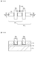
- a layout of the main part of the active load portion according to the first embodiment is shown in FIG. 7A, and a cross-sectional view taken along the line AA of FIG.
- PMOS transistor P-channel MOS type field effect transistor
- PMOS transistor Tr 4 constituting the active load unit 1413 according to the first embodiment, any a gate length and gate width for example, four PMOS transistors 51 1, 51 2, 51 3, 51 4, the common active region It has become the structure connected in series so that it might become. Specifically, 1 four PMOS transistors 51, 51 2, 51 3, 51 4 are formed in the active region 54 made of N-well region surrounded by the isolation portions 53 on the P-type semiconductor substrate 52 , Connected in series through the active area 54.
- the PMOS transistor Tr 4 according to Example 1 as a control terminal for controlling the current, for example, the four gate terminals (drawing, is the same in each of the embodiments are illustrated.
- the gate electrode having 55 1, 55 2, 55 3, 55 4.
- the four gate terminals 55 1 55 2 55 3 55 4 are electrically connected in common by the wiring 56, and a contact is made between each of the gate terminals 55 1 55 2 55 3 55 4.
- the drain region and the source region are alternately connected in series.
- a source terminal 57 and a drain terminal 58 are electrically connected through the interlayer film 60 to P + regions at both ends in the active region 54 to be a source region and a drain region.
- a layout example in the case where four PMOS transistors 51 1 , 51 2 , 51 3 , and 514 having the same gate length and gate width as the active load unit 1413 according to the first embodiment are designed with a multi-finger structure is a reference example. As shown in FIG. 7B.
- the transconductance gm for d is shown in FIG.
- the layout of the first embodiment as compared with the layout of the reference example, the drain current I d is the mutual conductance gm of around 1 ⁇ A is reduced by one digit.
- the reduction of the mutual conductance gm of the active load unit 1413 can reduce the noise of the comparator 141 itself (lower the noise). This is specifically described below.
- the random noise component of the N channel MOS type field effect transistor (hereinafter abbreviated as “NMOS transistor”) Tr 2 constituting the differential input unit 1411 is V n — n 2 the conductance and gm _n. Further, the random noise component of the PMOS transistor Tr 4 constituting the active load 1413 and V n_p 2, the mutual conductance and gm _p. At this time, the total random noise V n 2 output from the comparator 141 is expressed by the following equation (1).
- the total random noise V n 2 output from the comparator 141 is represented by the sum of the random noise component V n_n 2 of the differential input section 1411, a random noise component V n_p 2 active load unit 1413.
- the random noise component V n — p 2 of the active load unit 1413 contributes to the random noise V n 2 of the comparator 141 in proportion to the mutual conductance gm — p of the PMOS transistor Tr 4 constituting the active load unit 1413.
- the random noise spectrum of the transistor itself which constitutes the active load unit 1413 shown in FIG. 10 at the gate input referred noise SV g.
- the random noise component V n — p of the active load portion 1413 is 2 itself increases.
- the standard deviation of the output offset voltage variation of the comparator 141 can also be improved.
- the output offset voltage variation is a quantity that indicates the degree of variation of the output voltage of the comparator 141 which is generated due to the characteristic variation of the elements constituting the comparator 141. If the standard deviation of this output offset voltage variation is large, fixed pattern noise will increase. The output offset voltage variation becomes more pronounced as the threshold voltage variation of the transistors constituting the comparator 141 is larger.
- the standard deviation of the NMOS transistor Tr 2 of the threshold voltage variation of the differential input section 1411 as a sigma VTH_N, the mutual conductance and gm _n. Further, the standard deviation of the threshold voltage variation of the PMOS transistor Tr 4 constituting the active load 1413 and sigma Vth_p, the mutual conductance and gm _p. At this time, the standard deviation ⁇ Vout of the output offset voltage variation of the comparator 141 is expressed by the following equation (2).
- the standard deviation sigma Vout of the output offset voltage variation of the comparator 141 the standard deviation of the threshold voltage variation sigma VTH_N the NMOS transistor Tr 2 of the differential input section 1411, the threshold voltage variation of the PMOS transistor Tr 4 active load unit 1413 It is determined by the sum of ⁇ Vth_p .
- the standard deviation ⁇ Vth — p of the threshold voltage variation of the PMOS transistor Tr 4 of the active load unit 1413 contributes to the standard deviation ⁇ Vout of the output offset voltage variation in proportion to the mutual conductance gm — p .
- the threshold voltage variation generally depends on the gate area of the MOS field effect transistor. Therefore, the threshold voltage variations of the PMOS transistors constituting the active load unit 1413 are the same in the layout of the first embodiment and the layout according to the reference example. Therefore, the standard deviation sigma VTH_N the NMOS transistor Tr 2 of the threshold voltage variation of the differential input section 1411, since not change the layout of the layout and a reference example of Example 1, the standard deviation of the output offset voltage variation sigma As for Vout , the layout of the first embodiment is smaller than the layout of the reference embodiment.
- the improvement effect of the random noise and the output voltage variation of the comparator 141 when the layout of the first embodiment is used is described in FIG. 11 in comparison with the case of using the layout of the reference example.
- the comparator 141 when using a layout of Example 1, about 85% of the mutual conductance gm _p active load unit 1413, a noise component (gm _p / gm _n) about 60% of about ⁇ V n_p Improvement is expected. Further, an improvement of about 15% is expected for the total noise V n of the comparator 141, and about 35% for the standard deviation ⁇ Vout of the output offset voltage variation.
- Example 2 The second embodiment is a modification of the first embodiment, in which active regions are separated, and one transistor is formed in one active region, that is, a plurality of transistors are dispersedly arranged in different active regions. It is.
- the layout of the main part of the active load part based on Example 2 is shown to FIG. 12A.
- each of the electrically isolated for example two active regions 54 1, 54 2, a PMOS transistor is formed one by one structure ing.
- a plurality (e.g., two) on each active region 54 1, 54 2, and the gate terminal 55 1, 55 2 is arranged to form two PMOS transistors 51 1, 51 2 . Then, in the two PMOS transistors 51 1 and 51 2 , the active region 54 1 and the active region 54 2 are connected by the wire 59, and the two gate terminals 55 1 and 55 2 for controlling the current are electrically Are commonly connected.
- the PMOS transistor Tr 4 is divided into, for example, two PMOS transistors 51 1 and 51 2 , and these PMOS transistors 51 1 and 51 2 are connected in series. It has a structure.
- the case where a total of two PMOS transistors 51 1 and 51 2 are configured is illustrated by electrically dividing the active region into two and arranging one gate terminal in each active region.
- the number of transistors is not limited to two, and may be three or more.
- three gate terminals for controlling current are arranged in each of three or more separated active regions, and are electrically connected in common by interconnection 56. It will be.
- the arrangement of both transistors is attained. With such a layout, it is possible to reduce the relative characteristics variations between the PMOS transistor Tr 3 and the PMOS transistor Tr 4, can reduce the output variation of the comparator 141.
- a method of dividing the PMOS transistor Tr 4 is in view of the channel width W required to obtain the characteristics required in the circuit design, as in Example 3 to Example 5 below and in Example 2, various layouts You can take
- the third embodiment is a modification of the first embodiment, in which active regions are separated and a plurality of transistors are formed in one active region.
- the layout of the main part of the active load unit according to the third embodiment is shown in FIG.
- each of the electrically isolated for example two active regions 54 1, 54 2, PMOS transistor are multiple (e.g., three) by The structure is
- the active region 54 1 is formed three gate terminals 55 1, 55 2, 55 3 is the arrangement of three PMOS transistors 51 1, 51 2, 51 3. Further, in the active region 542 to form a three gate terminals 55 4, 55 5, 55 6 are disposed three PMOS transistors 51 4, 51 5, 51 6.
- Three PMOS transistors 51 1 formed in the active region 54 1, 51 2, 51 3 are connected in series to each other through active regions 54 1, three PMOS transistors formed in the active region 54 2 51 4, 51 5, 51 6 are connected in series to each other through the active region 54 2. Then, by the active region 54 1 and the active region 54 2 are connected by wires 59, six PMOS transistors 51 1-51 6 are connected in series. Further, in the six PMOS transistors 51 1 to 51 6 , six gate terminals 55 1 to 55 6 for controlling the current are electrically connected in common by the wiring 56.
- the case where a total of six PMOS transistors 51 1 to 51 6 are configured is illustrated by electrically dividing the active region into two and arranging three gate terminals in each active region.
- the number of transistors is not limited to six.
- three or more gate terminals may be arranged in each of two electrically isolated active regions, or the active regions may be electrically separated into three or more, and each of the active regions may be separated.
- Two or three or more gate terminals may be arranged.
- the plurality of gate terminals for controlling the current are electrically connected in common by the wiring 56.
- Example 4 The fourth embodiment is a modification of the first embodiment, and is an example of a combination of parallel connection and series connection of two or more transistors.
- the layout of the main part of the active load part concerning Example 4 is shown in FIG.
- PMOS transistor Tr 4 constituting the active load unit 1413 according to the fourth embodiment, each of the electrically isolated for example four active regions 54 1-54 4, a PMOS transistor is formed one by one structure ing.
- disposed gate terminal 55 1 is in the active region 54 1 to form a PMOS transistor 51 1, to form a PMOS transistor 51 2 are disposed gate terminal 55 2 is in the active region 54 in 2 . Then, the PMOS transistor 51 1 and the PMOS transistor 51 2, that the gate terminals 55 1, 55 2 is a common terminal, the source region and between the drain region are electrically connected to each other in common, respectively, connected in parallel
- the configuration is
- a gate terminal 55 3 in the active region 54 within 3 to form a PMOS transistor 51 3 to form a PMOS transistor 51 4 gate terminal 55 4 in the active region 54 within 4 is arranged. Then, the PMOS transistor 51 3 and the PMOS transistor 51 4, that the gate terminals 55 3, 55 4 is a common terminal, the source region and between the drain region are electrically connected to each other in common, respectively, connected in parallel.
- the configuration is
- the PMOS transistors 51 1 and the PMOS transistor 51 2 connected in parallel, the PMOS transistors 51 3 and the PMOS transistor 51 4 which are connected in parallel, are connected in series by wiring 59. That, PMOS transistor Tr 4 constituting the active load unit 1413 according to the fourth embodiment, a set of parallel connection of PMOS transistors 51 1 and the PMOS transistor 51 2, PMOS transistors 51 3 and a set of PMOS transistors 51 4 connected in parallel And are connected in series.
- the gate terminals 55 1 and 55 2 for controlling the current and the gate terminals 55 3 and 55 4 are electrically connected in common by the wiring 56.
- the case where the number of transistors in parallel connection is two is exemplified, but the number is not limited to two, and three or more parallel connections may be made.
- the number of series connections of the parallel connection set is not limited to two, and may be three or more series connection.
- Example 5 The fifth embodiment is a modification of the first embodiment, and is an example of a combination of series connection and parallel connection of two or more transistors.
- the layout of the main part of the active load part concerning Example 5 is shown in FIG.
- each PMOS transistor Tr 4 constituting the active load unit 1413 according to the fifth embodiment, formed on each of the electrically isolated for example two active regions 54 1, 54 2, each PMOS transistor are multiple (e.g., two) The structure is
- two gate terminals 55 1 and 55 2 are disposed in the active region 54 1 to form two PMOS transistors 51 1 and 51 2 . Then, in the PMOS transistors 51 1, 51 2, the gate terminals 55 1, 55 2 and between the source region to each other are electrically connected in common, respectively. Thus, they are connected in series to each other and PMOS transistor 51 1 and the PMOS transistor 51 2.
- active region 54 2 in the two gate terminals 55 3, 55 4 is arranged to form two PMOS transistors 51 3, 51 4. And these in the PMOS transistors 51 3, 51 4, each of the gate terminals 55 3, 55 4 and between the source region are connected to each other electrically in common, respectively. Thus, they are connected in series to each other and PMOS transistor 51 3 and the PMOS transistor 51 4.
- the PMOS transistors 51 1 and the PMOS transistor 51 2 connected in series, and the PMOS transistors 51 3 and the PMOS transistor 51 4 connected in series, are connected in parallel by wires 59. That, PMOS transistor Tr 4 constituting the active load unit 1413 according to the fifth embodiment, a pair of PMOS transistors 51 1 and the PMOS transistor 51 2 connected in series, the PMOS transistors 51 3 and the PMOS transistor 51 4 of serially connected pairs And are connected in parallel.
- the gate terminals 55 1 and 55 2 for controlling the current and the gate terminals 55 3 and 55 4 are electrically connected in common by the wiring 56.
- Example 6 The sixth embodiment is a modification of the first embodiment and is an example in which a dummy gate terminal is disposed in the active region.
- the layout of the main part of the active load part concerning Example 6 is shown in FIG.
- a plurality in the active region 54 1 (e.g., four) with the gate terminal 55 1-55 4 are arranged in a plurality (e.g., 4 ) And dummy gate terminals 61 1 to 61 4 are arranged.
- a four PMOS transistors 51 1-51 4 are arranged four gate terminals 55 1-55 4 in the active region 54 1.
- the four gate terminals 55 1 to 55 4 for controlling the current are electrically connected in common by the wiring 56.
- two dummy gate terminals 61 1 and 61 2 are arranged on one end side in the same active region 54 1 , and two dummy gate terminals 61 3 and 61 4 are arranged on the other end side. It is arranged. A ground potential is usually applied to these dummy gate terminals 61 1 to 61 4 . However, the dummy gate terminals 61 1 to 61 4 may be in a floating state.
- PMOS transistor Tr 4 constituting the active load unit 1413 according to the sixth embodiment, it is possible to obtain the following effects, effects.
- the density at which the gate terminals are arranged becomes constant, so that the coarse / dense dependence can be alleviated.
- the processing variation can be reduced, and the processing accuracy can be improved, so that the characteristic variation of the PMOS transistor Tr 4 can be reduced.
- the functions and effects are the same as in the seventh embodiment.
- Example 7 The seventh embodiment is a modification of the sixth embodiment and is an example in which a dummy gate terminal is disposed between transistors constituting a circuit when the dummy gate terminal is disposed in the active region.
- the layout of the main part of the active load part concerning Example 7 is shown in FIG.
- the sixth embodiment with respect to the four PMOS transistors 51 1 to 51 4 formed in the peripheral portion of the transistors constituting the circuit, specifically, in the central portion in the active region 54 1 , dummy on both sides thereof.
- the configuration is such that the gate terminals 61 1 to 61 4 of the above are arranged.
- Example 7 disposed between the PMOS transistors 51 1, 51 2 and the PMOS transistor 51 3, 51 4, for example, two dummy gate terminal 61 2, 61 3, the active region 54
- the dummy gate terminals 61 1 and 61 4 are disposed on both end sides in the first embodiment.
- the gate terminals 55 1 and 55 2 for controlling the current and the gate terminals 55 3 and 55 4 are electrically connected in common by the wiring 56. Further, for example, the ground potential is applied to the dummy gate terminals 61 1 to 61 4 .
- PMOS transistor Tr 4 constituting the active load unit 1413 according to the seventh embodiment can also achieve effects similar to the PMOS transistor Tr 4 constituting the active load unit 1413 according to the sixth embodiment, the effects. That is, since the dependence on the density can be relaxed, the processing accuracy can be improved.
- Example 1 to Example 7 is an example of one of the PMOS transistor Tr 4 constituting the active load unit 1413 in the circuit configuration of the comparator 141 shown in FIG. 6A comprises a field effect transistor.
- the eighth embodiment is an example in which both of the PMOS transistors Tr 3 and Tr 4 constituting the active load portion 1413 are field effect transistors.
- the active load unit 1413 has a structure in which both PMOS transistors Tr 3 and Tr 4 are respectively formed of a plurality of (for example, three) PMOS transistors and formed in the same active region 54 1 . ing.
- the active region 54 1, three gate terminals 55 31-55 33 are arranged to form a three PMOS transistors 51 31-51 33 of the PMOS transistor Tr 3.
- Three gate terminals 55 41 to 55 43 are arranged in the same active region 54 1 adjacent to PMOS transistor Tr 3 to form three PMOS transistors 51 41 to 51 43 of PMOS transistor Tr 4.
- the both ends of the active region 54 1, dummy gate terminals 61 1, 61 2 are disposed. For example, a ground potential is applied to these dummy gate terminals 61 1 and 61 2 .
- the active load unit 1413 includes a plurality of (three in this example) PMOS transistors in which the PMOS transistors Tr 3 and Tr 4 are connected in series, and both PMOSs are used.
- the active regions of the transistors Tr 3 and Tr 4 are shared.
- the drain terminal 58 1 from both ends of the active region 54 1, 58 2 is drawn out, the source terminal 57 is a common terminal for both PMOS transistors Tr 3, Tr 4.
- the active load unit 1413 According to the active load unit 1413 according to the eighth embodiment, and common source region between the PMOS transistor Tr 3 and the PMOS transistor Tr 4 constituting the active load unit 1413, a structure drawing the source terminal 57 as a common terminal As a result, the entire circuit area of the active load unit 1413 can be reduced.
- the second embodiment of the present disclosure is an example in which a transistor forming the comparator 141 is a Fin-FET.
- the Fin-FET can be formed by a high dielectric constant / metal gate (high-K / metal gate) process.
- the Fin-FET is a transistor structure in which a planar (planar) transistor is expanded into a three-dimensional structure to enhance high-speed operation performance and power saving performance.
- the technology of the present disclosure that is, the technology of making the transistors constituting the active load portion 1413 a structure having a plurality of control terminals (gate terminals) and electrically connecting the plurality of control terminals in common. It can apply. Specific examples of the second embodiment will be described below as Examples 9 to 13.
- Example 9 one of the transistors Tr 4 constituting the active load unit 1413 is an example consisting of one Fin-FET.
- the layout of the main part of the active load portion according to the ninth embodiment is shown in FIG. 19A, and the cross-sectional view of the arrow cross section taken along the line BB in FIG. 19A is shown in FIG.
- the insulating film 72 on the semiconductor substrate 71 is deposited, becomes over the insulating film 72 fin (Fin) 73 is provided structure There is. Then, a plurality of (for example, two) gate terminals 55 1 and 55 2 are disposed in the recess of the fin 73 to form two PMOS transistors 51 1 and 51 2 .
- the source terminal 57 and the drain terminal 58 are electrically connected to both ends of the fin 73 which is to be the source region and the drain region. Further, two gate terminals 55 1 and 55 2 for controlling the current are electrically connected in common by the wiring 56.
- PMOS transistor Tr 4 constituting the active load unit 1413 according to Embodiment 9 is constituted by one Fin-FET in which two or more gate terminals are arranged, all the gates for controlling the current The terminals are electrically connected in common (commonized).
- Example 10 is a variation of Example 9, one of the transistors Tr 4 constituting the active load unit 1413 is an example including a plurality of Fin-FET connected in series. The layout of the main part of the active load part concerning Example 10 is shown to FIG. 20A.
- Example 9 illustrates the case where the PMOS transistor Tr 4 is composed of one Fin-FET.
- the PMOS transistor Tr 4 constituting the active load unit 1413 according to Embodiment 10 a plurality (e.g., two) has become a Fin-FET of connected in series.
- two fins 73 1 and 73 2 are connected in series by a wire 59, and gate terminals 55 1 and 55 2 arranged on these fins 73 1 and 73 2 are electrically shared by a wire 56. It is connected.
- the PMOS transistor Tr 4 constituting the active load unit 1413 according to Embodiment 10 two or more Fin-FET are connected in series by wiring, electrical all the gate terminal for controlling the current by wires In the common connection.
- Example 11 is a modification of Example 9, one of the transistors Tr 4 constituting the active load unit 1413 is an example including a plurality of Fin-FET connected in parallel. The layout of the main part of the active load part concerning Example 11 is shown to FIG. 20B.
- the PMOS transistor Tr 4 constituting the active load unit 1413 according to Example 11 the PMOS transistor Tr 4 constituting the active load unit 1413 according to Embodiment 9 multiple (e.g., four) becomes a structure connected in parallel There is. Specifically, the juxtaposed four fins 73 1-73 4, together with the respective source regions are connected in common by the source wiring 57, each of the drain regions are connected in common by a drain wiring 58. Further, gate terminals 55 1 and 55 2 are common terminals among the four fins 73 1 to 734 respectively, and both gate terminals 55 1 and 55 2 are electrically connected in common by the wiring 56. .
- the PMOS transistor Tr 4 constituting the active load unit 1413 according to Example 11 Fin-FET is connected in parallel with two or more connecting all the gate terminal for controlling the current in the common electrically
- the structure is
- Example 12 The twelfth embodiment is a modification of the tenth embodiment, and is an example in which one transistor Tr 4 constituting the active load portion 1413 is configured by connecting in parallel a plurality of sets of Fin-FETs connected in series. is there.
- the layout of the main part of the active load part concerning Example 12 is shown to FIG. 21A.
- the PMOS transistor Tr 4 constituting the active load unit 1413 according to Embodiment 12 a plurality (e.g., two) becomes a structure connected in parallel There is. More specifically, the two fins 73 1, 73 2 wiring 59 1 are connected in series, similarly, two fins 73 3, 73 4 are connected in series by the wiring 599 2. Then, it is arranged a gate terminal 55 1 is astride the fin 73 1 and the fin 73 3, is disposed a gate terminal 55 2 is across the fins 73 2 and the fins 73 4, gate terminal 55 1, 55 2 wiring 56 Are electrically connected in common.
- the PMOS transistor Tr 4 constituting the active load unit 1413 according to Embodiment 12 series connected Fin-FET is connected in parallel with two or more, all the gate terminal for controlling the current electrical Commonly connected to the
- Example 13 The thirteenth embodiment is a modification of the ninth embodiment, and is an example in which one transistor Tr 4 constituting the active load portion 1413 is configured by connecting in series a plurality of sets of Fin-FETs connected in parallel. is there.
- the layout of the main part of the active load part concerning Example 13 is shown to FIG. 21B.
- the PMOS transistor Tr 4 constituting the active load unit 1413 according to Embodiment 13 multiple (e.g., two) are connected in parallel, the parallel connection A plurality of (for example, two) sets of are connected in series.
- are connected in parallel by the drain wiring 58 become fins 73 1 and the fin 73 2 Togagumi
- the source wiring 57 become fin 73 3 and the fin 73 4 Togagumi.
- gate terminals 55 1 and 55 2 are common terminals among the four fins 73 1 to 734 respectively, and both gate terminals 55 1 and 55 2 are electrically connected in common by the wiring 56. .
- Fin-FET is connected in parallel with two or more in series a set of Fin-FET of the parallel connection are two sets or more And all the gate terminals that control the current are electrically connected in common.
- the PMOS transistor Tr 4 constituting the active load unit 1413 according to Embodiment 12 series connected Fin-FET is connected in parallel with two or more, all the gate terminal for controlling the current electrical Commonly connected to the
- the layout of the common centroid arrangement can be made as in the case of the second to fifth embodiments described above. it can. By the layout of the common centroid arrangement, the same operation and effect as those of the second to fifth embodiments can be obtained.
- the width of the fin 73 of the Fin-FET is a fixed value that can not be freely changed due to processing problems, it is preferable to make it as in Example 11 (FIG. 20B) to Example 13 (FIG. 21B). Since the total channel length W can be set long, noise reduction and variation in transistor characteristics can be further reduced.
- Increasing the drain resistance R ds is an important characteristic in order to ensure the operation stability of the analog circuit using the MOS type field effect transistor. By connecting a plurality of transistors in series to increase the total gate length, it is possible to obtain a drain resistance R ds similar to the previous generation in addition to noise reduction.
- various layouts can be taken as in the ninth to thirteenth embodiments in balance with the channel width W necessary to obtain the characteristics required for the circuit design.
- the third embodiment of the present disclosure is an example in which a transistor constituting the comparator 141 is a bipolar transistor.
- An example of a circuit configuration of the comparator 141 composed of a bipolar transistor is shown in FIG.
- the differential input unit 1411 includes, for example, NPN bipolar transistors Tr 11 and Tr 12 whose emitter terminals are commonly connected.
- the base terminal of the bipolar transistor Tr 11, the reference signal is inputted through the capacitor C 1, the base terminal of the bipolar transistor Tr 12, the pixel signal is input via the capacitor C 2.
- the constant current source 1412 is connected between the emitter common connection node of the bipolar transistors Tr 11 and Tr 12 and the node of the reference potential (for example, the ground potential).
- Active load portion 1413 is formed of PNP bipolar transistors Tr 13 and Tr 14 connected between the collector terminals of bipolar transistors Tr 11 and Tr 12 and the node of power supply voltage V CC .
- the base terminals of the bipolar transistors Tr 13 and Tr 14 are connected in common. Further, the bipolar transistor Tr 13 has a base and collector terminals are connected together. That is, the bipolar transistors Tr 13 and Tr 14 constitute a current mirror circuit. Then, from the common collector connection node of the bipolar transistor Tr 12 and the bipolar transistor Tr 14, the output V out is derived.
- Example 14 The fourteenth embodiment is an example in which active regions are separated, and one bipolar transistor is formed in one active region.
- the layout of the main part of the active load unit according to the fourteenth embodiment is shown in FIG.
- the bipolar transistor Tr 14 constituting the active load portion 1413 according to the fourteenth embodiment is composed of a plurality (for example, two) of PNP bipolar transistors, and the emitter terminal and the collector terminal are alternately connected in series alternately to control the current.
- the base terminal of is commonly used.
- the bipolar transistor 85 1 and bipolar transistor 85 2 is dispersed to the arrangement of the different active regions 1 and the active region 81 2.
- an emitter terminal 83 1 of the bipolar transistor 85 1 are connected by a collector terminal 842 and the wiring 86 of the bipolar transistor 85 2, the base terminal 82 1, 82 for controlling the current
- the two wires 87 are electrically connected in common and made common.
- the collector wiring 88 is connected to the collector terminal 84 1 of the bipolar transistor 85 1
- emitter wiring 89 is connected to the emitter terminal 83 2 of the bipolar transistor 85 2.
- Example 15 The fifteenth embodiment is an example in which a plurality of bipolar transistors are formed in one active region.
- the layout of the main part of the active load unit according to the fifteenth embodiment is shown in FIG.
- bipolar transistor Tr 14 constituting the active load portion 1413 according to the fifteenth embodiment, two bipolar transistors having a common base terminal are arranged in one active region, and the emitter terminals of the two bipolar transistors are arranged together. It has a structure in which a collector terminal is connected in series. Specifically, two bipolar transistors 85 1 and 85 2 are disposed in one active region 81, and the base terminals of these bipolar transistors 85 1 and 85 2 are a common base terminal 82. Then, the emitter terminal 83 1 of the bipolar transistor 85 1 is connected by a collector terminal 842 and the wiring 86 of the bipolar transistor 85 2.
- the bipolar transistor Tr 14 constituting the active load portion 1413 according to the fifteenth embodiment, since the base terminal 82 is shared between the bipolar transistors 85 1 and 85 2 , simple series connection is performed as in the fourteenth embodiment.
- the total transistor area can be reduced more than in the case of
- Example 16 A sixteenth embodiment is a modification of the fifteenth embodiment.
- the layout of the main part of the active load unit according to the sixteenth embodiment is shown in FIG.
- Bipolar transistor Tr 14 which constitutes the active load unit 1413 according to Embodiment 16 connects the bipolar transistor Tr 14 which constitutes the active load unit 1413 according to Example 15 a plurality (e.g., two) in series, all of the base
- the structure is common to the terminals.
- two bipolar transistors 85 1 and 85 2 are formed in each of two active regions 81 1 and 81 2 , and the common base terminals 82 1 and 82 2 of both are formed by the wiring 87. Commonly connected.
- an emitter terminal 83 1 of the bipolar transistor 85 1, and the collector terminal 84 2 of the bipolar transistor 85 2 are connected by wires 86 1, 2. Further, in the active region 81 1, 81 between 2, the emitter terminal 83 2 of the bipolar transistor 85 and second active region 81 1 side, the collector terminal 84 1 and the wiring 86 3 of the active region 81 2 side bipolar transistor 85 1 It is connected.
- the layout can be made in the common centroid arrangement, as in the case of the second to fifth embodiments described above.
- the layout of the common centroid arrangement the same operation and effect as those of the second to fifth embodiments can be obtained.
- Application Example 1 As another application example, for example, an analog switch used in various sensor circuits such as light, temperature, odor and the like can be illustrated.
- Application Example 1 is an example applied to, for example, an analog switch used in a photodetector.
- An example of a circuit of an analog switch according to Application Example 1 is shown in FIG. 26A, and waveforms of detection signals and output signals of the analog switch are shown in FIG. 26B.
- the photodetector compares the detection signal detected using a photodiode (not shown) with the reference voltage V ref, and the output signal V out responds to the comparison result to determine whether light is detected or not. It is The technology of the present disclosure can be applied to a comparator 141 in which a detection signal is weak and a high SN ratio is required in various sensor circuits such as a light detector.
- Application Example 2 is an example applied to a triangular wave generation circuit required when controlling an electric motor or the like by a PWM (Pulse Width Modulation) method.
- FIG. 27A shows a circuit example of a triangular wave generation circuit according to application example 2
- FIG. 27B shows an output waveform of the triangular wave generation circuit.
- a triangular wave generation circuit according to Application Example 2 has a known circuit configuration including two comparators 141 1 and 1412, eight resistance elements R 1 to R 8 , and two capacitance elements C 1 and C 2. It has become. Against comparators 141 1, 141 2 constituting the triangular-wave generating circuit, it is possible to apply the techniques of this disclosure.
- Application Example 3 is an example applied to a digital-analog converter.
- a circuit example of a digital-analog converter according to application example 3 is shown in FIG.
- the digital-analog converter according to application example 3 is called a weight resistance type DA converter.
- the digital-to-analog converter according to application example 3 uses the adder circuit including the comparator 141 and the resistive element, and the output voltage is proportional to each bit of the digital signal in proportion to the resistance value of the resistive element. And a well-known circuit configuration for converting into an analog signal.
- the technology of the present disclosure can be applied to the comparator 141 that constitutes this digital-analog converter.
- comparators are used in various electronic devices such as various measuring instruments, AV devices, and home appliances distributed in the world, but those skilled in the art can apply the technology of the present disclosure to those comparators. , Easy to judge.
- the technology of the present disclosure is not limited to application to a solid-state imaging device that detects the distribution of incident light quantity of visible light and captures an image as an image, and images distribution of incident quantity such as infrared rays, X-rays, or particles as an image
- the present invention is applicable to all solid-state imaging devices.
- the CMOS image sensor 1 according to the present embodiment described above can be used for various devices that sense light such as visible light, infrared light, ultraviolet light, and X-rays as shown in FIG. 29, for example. Specific examples of various devices are listed below.
- a device that captures images for viewing such as a digital camera or a portable device with a camera function-For safe driving such as automatic stop, recognition of driver's condition, etc.
- a device provided for traffic such as an on-vehicle sensor for capturing images of the rear, surroundings, inside of a car, a monitoring camera for monitoring a traveling vehicle or a road, a distance measuring sensor for measuring distance between vehicles, etc.
- Devices used for home appliances such as TVs, refrigerators, air conditioners, etc. to perform imaging and device operation according to the gesture ⁇ Endoscopes, devices for performing blood vessel imaging by receiving infrared light, etc.
- Equipment provided for medical and healthcare use-Equipment provided for security such as surveillance cameras for crime prevention, cameras for personal identification, etc.-Skin measuring equipment for photographing skin, photographing for scalp Beauty, such as microscope
- Such action camera or wearable cameras provided by equipment and sports applications such as for the use, such as a camera for monitoring a sports state of the apparatus, groves and crops that are provided for use in, is provided for use in agricultural equipment
- an imaging apparatus such as a digital still camera or video camera
- a portable terminal apparatus having an imaging function such as a cellular phone
- an electronic apparatus such as a copying machine using a solid-state imaging device as an image reading unit
- FIG. 30 is a block diagram showing a configuration of an imaging device which is an example of the electronic device of the present disclosure.
- an imaging apparatus 100 includes an imaging optical system 101 including a lens group, an imaging unit 102, a DSP circuit 103, a frame memory 104, a display device 105, a recording device 106, an operation system 107, And a power supply system 108 and the like.
- the DSP circuit 103, the frame memory 104, the display device 105, the recording device 106, the operation system 107, and the power supply system 108 are connected to one another via the bus line 109.
- the imaging optical system 101 captures incident light (image light) from a subject and forms an image on an imaging surface of the imaging unit 102.
- the imaging unit 102 converts the light amount of incident light focused on the imaging surface by the optical system 101 into an electrical signal in pixel units and outputs the electrical signal as a pixel signal.
- the DSP circuit 103 performs general camera signal processing such as white balance processing, demosaicing processing, gamma correction processing and the like.
- the frame memory 104 is suitably used for storing data in the process of signal processing in the DSP circuit 103.
- the display device 105 includes a panel type display device such as a liquid crystal display device or an organic EL (electro luminescence) display device, and displays a moving image or a still image captured by the imaging unit 102.
- the recording device 106 records a moving image or a still image captured by the imaging unit 102 in a recording medium such as a portable semiconductor memory, an optical disk, or a hard disk drive (HDD).
- a recording medium such as a portable semiconductor memory, an optical disk, or a hard disk drive (HDD).
- the operation system 107 issues operation commands for various functions of the imaging device 100 under the operation of the user.
- the power supply system 108 appropriately supplies various power supplies serving as operation power supplies of the DSP circuit 103, the frame memory 104, the display device 105, the recording device 106, and the operation system 107 to these supply targets.
- the CMOS image sensor 1 to which the technology according to the present disclosure described above is applied can be used as the imaging unit 102. According to the CMOS image sensor 1, since noise reduction can be achieved, a high quality photographed image with little noise can be obtained.
- the technology according to the present disclosure can be applied to various products.
- the technology according to the present disclosure is any type of movement, such as automobiles, electric vehicles, hybrid electric vehicles, motorcycles, bicycles, personal mobility, airplanes, drones, ships, robots, construction machines, agricultural machines (tractors), etc. It may be realized as a solid-state imaging device mounted on the body.
- FIG. 31 is a block diagram showing a schematic configuration example of a vehicle control system 7000 which is an example of a mobile control system to which the technology according to the present disclosure can be applied.
- Vehicle control system 7000 comprises a plurality of electronic control units connected via communication network 7010.
- the vehicle control system 7000 includes a drive system control unit 7100, a body system control unit 7200, a battery control unit 7300, an outside information detection unit 7400, an in-vehicle information detection unit 7500, and an integrated control unit 7600. .
- the communication network 7010 connecting the plurality of control units is, for example, an arbitrary standard such as CAN (Controller Area Network), LIN (Local Interconnect Network), LAN (Local Area Network), or FlexRay (registered trademark). It may be an in-vehicle communication network.
- CAN Controller Area Network
- LIN Local Interconnect Network
- LAN Local Area Network
- FlexRay registered trademark
- Each control unit includes a microcomputer that performs arithmetic processing in accordance with various programs, a storage unit that stores programs executed by the microcomputer or parameters used in various arithmetic operations, and drive circuits that drive devices to be controlled. Equipped with Each control unit is provided with a network I / F for communicating with other control units via the communication network 7010, and by wired communication or wireless communication with an apparatus or sensor inside or outside the vehicle. A communication I / F for performing communication is provided. In FIG.
- the integrated control unit 7600 a microcomputer 7610, a general-purpose communication I / F 7620, a dedicated communication I / F 7630, a positioning unit 7640, a beacon receiving unit 7650, an in-vehicle device I / F 7660, an audio image output unit 7670, An in-vehicle network I / F 7680 and a storage unit 7690 are illustrated.
- the other control units also include a microcomputer, a communication I / F, a storage unit, and the like.
- Drive system control unit 7100 controls the operation of devices related to the drive system of the vehicle according to various programs.
- drive system control unit 7100 includes a drive force generation device for generating a drive force of a vehicle such as an internal combustion engine or a drive motor, a drive force transmission mechanism for transmitting the drive force to the wheels, and a steering angle of the vehicle. It functions as a control mechanism such as a steering mechanism that adjusts and a braking device that generates a braking force of the vehicle.
- the drive system control unit 7100 may have a function as a control device such as an ABS (Antilock Brake System) or an ESC (Electronic Stability Control).
- Vehicle state detection unit 7110 is connected to drive system control unit 7100.
- the vehicle state detection unit 7110 may be, for example, a gyro sensor that detects an angular velocity of an axial rotational movement of a vehicle body, an acceleration sensor that detects an acceleration of the vehicle, or an operation amount of an accelerator pedal, an operation amount of a brake pedal, and steering of a steering wheel. At least one of the sensors for detecting the angle, the engine speed, the rotational speed of the wheel, etc. is included.
- Drive system control unit 7100 performs arithmetic processing using a signal input from vehicle state detection unit 7110 to control an internal combustion engine, a drive motor, an electric power steering device, a brake device, and the like.
- Body system control unit 7200 controls the operation of various devices equipped on the vehicle body according to various programs.
- the body control unit 7200 functions as a keyless entry system, a smart key system, a power window device, or a control device of various lamps such as a head lamp, a back lamp, a brake lamp, a blinker or a fog lamp.
- the body system control unit 7200 may receive radio waves or signals of various switches transmitted from a portable device substituting a key.
- Body system control unit 7200 receives the input of these radio waves or signals, and controls a door lock device, a power window device, a lamp and the like of the vehicle.
- the battery control unit 7300 controls the secondary battery 7310 which is a power supply source of the drive motor according to various programs. For example, information such as the battery temperature, the battery output voltage, or the remaining capacity of the battery is input to the battery control unit 7300 from the battery device provided with the secondary battery 7310. The battery control unit 7300 performs arithmetic processing using these signals, and performs temperature adjustment control of the secondary battery 7310 or control of a cooling device or the like provided in the battery device.
- Outside-vehicle information detection unit 7400 detects information outside the vehicle equipped with vehicle control system 7000.
- the imaging unit 7410 and the external information detection unit 7420 is connected to the external information detection unit 7400.
- the imaging unit 7410 includes at least one of a time-of-flight (ToF) camera, a stereo camera, a monocular camera, an infrared camera, and another camera.
- ToF time-of-flight
- an environment sensor for detecting the current weather or weather, or another vehicle, an obstacle or a pedestrian around the vehicle equipped with the vehicle control system 7000 is detected in the outside-vehicle information detection unit 7420, for example.
- the ambient information detection sensors at least one of the ambient information detection sensors.
- the environment sensor may be, for example, at least one of a raindrop sensor that detects wet weather, a fog sensor that detects fog, a sunshine sensor that detects sunshine intensity, and a snow sensor that detects snowfall.
- the ambient information detection sensor may be at least one of an ultrasonic sensor, a radar device, and a light detection and ranging (LIDAR) device.
- the imaging unit 7410 and the external information detection unit 7420 may be provided as independent sensors or devices, or may be provided as an integrated device of a plurality of sensors or devices.
- FIG. 32 shows an example of installation positions of the imaging unit 7410 and the external information detection unit 7420.
- the imaging units 7910, 7912, 7914, 7916, 7918 are provided at, for example, at least one of the front nose of the vehicle 7900, the side mirror, the rear bumper, the back door, and the upper portion of the windshield of the vehicle interior.
- An imaging unit 7910 provided in the front nose and an imaging unit 7918 provided in the upper part of the windshield in the vehicle cabin mainly acquire an image in front of the vehicle 7900.
- the imaging units 7912 and 7914 provided in the side mirror mainly acquire an image of the side of the vehicle 7900.
- An imaging unit 7916 provided in the rear bumper or back door mainly acquires an image behind the vehicle 7900.
- the imaging unit 7918 provided on the upper part of the windshield in the passenger compartment is mainly used to detect a leading vehicle or a pedestrian, an obstacle, a traffic light, a traffic sign, a lane, or the like.
- FIG. 32 illustrates an example of the imaging range of each of the imaging units 7910, 7912, 7914, and 7916.
- the imaging range a indicates the imaging range of the imaging unit 7910 provided on the front nose
- the imaging ranges b and c indicate the imaging ranges of the imaging units 7912 and 7914 provided on the side mirrors
- the imaging range d indicates The imaging range of the imaging part 7916 provided in the rear bumper or the back door is shown.
- a bird's-eye view of the vehicle 7900 as viewed from above can be obtained.
- the external information detection units 7920, 7922, 7924, 7926, 7928, and 7930 provided on the front, rear, sides, and corners of the vehicle 7900 and above the windshield of the vehicle interior may be, for example, ultrasonic sensors or radar devices.
- the external information detection units 7920, 7926, 7930 provided on the front nose of the vehicle 7900, the rear bumper, the back door, and the upper part of the windshield of the vehicle interior may be, for example, a LIDAR device.
- These outside-of-vehicle information detection units 7920 to 7930 are mainly used for detecting a preceding vehicle, a pedestrian, an obstacle or the like.
- the out-of-vehicle information detection unit 7400 causes the imaging unit 7410 to capture an image outside the vehicle, and receives the captured image data. Further, the external information detection unit 7400 receives detection information from the external information detection unit 7420 connected. When the out-of-vehicle information detection unit 7420 is an ultrasonic sensor, a radar device, or a LIDAR device, the out-of-vehicle information detection unit 7400 transmits ultrasonic waves or electromagnetic waves and receives information on the received reflected waves.
- the external information detection unit 7400 may perform object detection processing or distance detection processing of a person, a car, an obstacle, a sign, a character on a road surface, or the like based on the received information.
- the external information detection unit 7400 may perform environment recognition processing for recognizing rainfall, fog, road surface conditions and the like based on the received information.
- the external information detection unit 7400 may calculate the distance to an object outside the vehicle based on the received information.
- the external information detection unit 7400 may perform image recognition processing or distance detection processing for recognizing a person, a car, an obstacle, a sign, a character on a road surface, or the like based on the received image data.
- the external information detection unit 7400 performs processing such as distortion correction or alignment on the received image data, and combines the image data captured by different imaging units 7410 to generate an overhead image or a panoramic image. It is also good.
- the external information detection unit 7400 may perform viewpoint conversion processing using image data captured by different imaging units 7410.
- An in-vehicle information detection unit 7500 detects information in the vehicle.
- a driver state detection unit 7510 that detects a state of a driver is connected to the in-vehicle information detection unit 7500.
- the driver state detection unit 7510 may include a camera for imaging the driver, a biometric sensor for detecting the driver's biological information, a microphone for collecting sound in the vehicle interior, and the like.
- the biological sensor is provided, for example, on a seat or a steering wheel, and detects biological information of an occupant sitting on a seat or a driver who grips the steering wheel.
- the in-vehicle information detection unit 7500 may calculate the degree of fatigue or concentration of the driver based on the detection information input from the driver state detection unit 7510, or determine whether the driver does not go to sleep You may The in-vehicle information detection unit 7500 may perform processing such as noise canceling processing on the collected audio signal.
- the integrated control unit 7600 controls the overall operation in the vehicle control system 7000 in accordance with various programs.
- An input unit 7800 is connected to the integrated control unit 7600.
- the input unit 7800 is realized by, for example, a device such as a touch panel, a button, a microphone, a switch or a lever, which can be input operated by the passenger.
- the integrated control unit 7600 may receive data obtained by speech recognition of speech input by the microphone.
- the input unit 7800 may be, for example, a remote control device using infrared rays or other radio waves, or an external connection device such as a mobile phone or a PDA (Personal Digital Assistant) corresponding to the operation of the vehicle control system 7000.
- PDA Personal Digital Assistant
- the input unit 7800 may be, for example, a camera, in which case the passenger can input information by gesture. Alternatively, data obtained by detecting the movement of the wearable device worn by the passenger may be input. Furthermore, the input unit 7800 may include, for example, an input control circuit that generates an input signal based on the information input by the passenger or the like using the above-described input unit 7800 and outputs the generated signal to the integrated control unit 7600. The passenger or the like operates the input unit 7800 to input various data to the vehicle control system 7000 and instruct processing operations.
- the storage unit 7690 may include a ROM (Read Only Memory) that stores various programs executed by the microcomputer, and a RAM (Random Access Memory) that stores various parameters, calculation results, sensor values, and the like.
- the storage unit 7690 may be realized by a magnetic storage device such as a hard disk drive (HDD), a semiconductor storage device, an optical storage device, a magneto-optical storage device, or the like.
- HDD hard disk drive
- semiconductor storage device an optical storage device
- magneto-optical storage device or the like.
- the general-purpose communication I / F 7620 is a general-purpose communication I / F that mediates communication with various devices existing in the external environment 7750.
- General-purpose communication I / F 7620 is a cellular communication protocol such as GSM (registered trademark) (Global System of Mobile communications), WiMAX, LTE (Long Term Evolution) or LTE-A (LTE-Advanced), or wireless LAN (Wi-Fi)
- GSM registered trademark
- WiMAX Wireless LAN
- LTE Long Term Evolution
- LTE-A Long Term Evolution-A
- Wi-Fi wireless LAN
- Other wireless communication protocols such as (registered trademark), Bluetooth (registered trademark), etc. may be implemented.
- the general-purpose communication I / F 7620 is connected to, for example, an apparatus (for example, an application server or control server) existing on an external network (for example, the Internet, a cloud network, or an operator-specific network) via a base station or access point
- an apparatus for example, an application server or control server
- an external network for example, the Internet, a cloud network, or an operator-specific network
- the general-purpose communication I / F 7620 is a terminal (for example, a driver, a pedestrian or a shop terminal, or an MTC (Machine Type Communication) terminal) existing near the vehicle using, for example, P2P (Peer To Peer) technology. It may be connected with
- the dedicated communication I / F 7630 is a communication I / F that supports a communication protocol designed for use in a vehicle.
- the dedicated communication I / F 7630 may be a standard protocol such as WAVE (Wireless Access in Vehicle Environment), DSRC (Dedicated Short Range Communications), or cellular communication protocol, which is a combination of lower layer IEEE 802.11p and upper layer IEEE 1609, for example. May be implemented.
- the dedicated communication I / F 7630 is typically used for Vehicle to Vehicle communication, Vehicle to Infrastructure communication, Vehicle to Home communication, and Vehicle to Pedestrian. 2.) Perform V2X communication, a concept that includes one or more of the communication.
- the positioning unit 7640 receives a GNSS signal (for example, a GPS signal from a Global Positioning System (GPS) satellite) from, for example, a Global Navigation Satellite System (GNSS) satellite and executes positioning, thereby performing latitude, longitude, and altitude of the vehicle. Generate location information including The positioning unit 7640 may specify the current position by exchanging signals with the wireless access point, or may acquire position information from a terminal such as a mobile phone having a positioning function, a PHS, or a smartphone.
- GPS Global Positioning System
- GNSS Global Navigation Satellite System
- the beacon receiving unit 7650 receives, for example, radio waves or electromagnetic waves transmitted from a radio station or the like installed on a road, and acquires information such as the current position, traffic jams, closing times or required time.
- the function of the beacon reception unit 7650 may be included in the dedicated communication I / F 7630 described above.
- An in-vehicle apparatus I / F 7660 is a communication interface that mediates the connection between the microcomputer 7610 and various in-vehicle apparatuses 7760 existing in the vehicle.
- the in-car device I / F 7660 may establish a wireless connection using a wireless communication protocol such as wireless LAN, Bluetooth (registered trademark), NFC (Near Field Communication), or WUSB (Wireless USB).
- a wireless communication protocol such as wireless LAN, Bluetooth (registered trademark), NFC (Near Field Communication), or WUSB (Wireless USB).
- the in-vehicle device I / F 7660 is connected via a connection terminal (not shown) (and, if necessary, a cable) via USB (Universal Serial Bus), HDMI (High-Definition Multimedia Interface), or MHL (Mobile)
- USB Universal Serial Bus
- HDMI High-Definition Multimedia Interface
- MHL Mobile
- the in-vehicle device 7760 may include, for example, at least one of a mobile device or wearable device owned by a passenger, or an information device carried in or attached to a vehicle. Further, the in-vehicle device 7760 may include a navigation device for performing a route search to any destination.
- the in-vehicle device I / F 7660 exchanges control signals or data signals with these in-vehicle devices 7760.
- the in-vehicle network I / F 7680 is an interface that mediates communication between the microcomputer 7610 and the communication network 7010.
- the in-vehicle network I / F 7680 transmits and receives signals and the like in accordance with a predetermined protocol supported by the communication network 7010.
- the microcomputer 7610 of the integrated control unit 7600 is connected via at least one of a general-purpose communication I / F 7620, a dedicated communication I / F 7630, a positioning unit 7640, a beacon reception unit 7650, an in-vehicle device I / F 7660, and an in-vehicle network I / F 7680.
- the vehicle control system 7000 is controlled in accordance with various programs based on the information acquired. For example, the microcomputer 7610 calculates a control target value of the driving force generation device, the steering mechanism or the braking device based on the acquired information inside and outside the vehicle, and outputs a control command to the driving system control unit 7100. It is also good.
- the microcomputer 7610 realizes the function of an advanced driver assistance system (ADAS) including collision avoidance or shock mitigation of a vehicle, follow-up traveling based on an inter-vehicle distance, vehicle speed maintenance traveling, vehicle collision warning, vehicle lane departure warning, etc. Cooperative control for the purpose of In addition, the microcomputer 7610 automatically runs without using the driver's operation by controlling the driving force generating device, the steering mechanism, the braking device, etc. based on the acquired information of the surroundings of the vehicle. Coordinated control may be performed for the purpose of driving and the like.
- ADAS advanced driver assistance system
- the microcomputer 7610 is information acquired via at least one of a general-purpose communication I / F 7620, a dedicated communication I / F 7630, a positioning unit 7640, a beacon reception unit 7650, an in-vehicle device I / F 7660, and an in-vehicle network I / F 7680. Based on the above, three-dimensional distance information between the vehicle and an object such as a surrounding structure or a person may be generated, and local map information including the peripheral information of the current position of the vehicle may be created. Further, the microcomputer 7610 may predict a danger such as a collision of a vehicle or a pedestrian or the like approaching a road or the like on the basis of the acquired information, and may generate a signal for warning.
- the warning signal may be, for example, a signal for generating a warning sound or lighting a warning lamp.
- the audio image output unit 7670 transmits an output signal of at least one of audio and image to an output device capable of visually or aurally notifying information to a passenger or the outside of a vehicle.
- an audio speaker 7710, a display unit 7720, and an instrument panel 7730 are illustrated as output devices.
- the display unit 7720 may include, for example, at least one of an on-board display and a head-up display.
- the display portion 7720 may have an AR (Augmented Reality) display function.
- the output device may be another device such as a headphone, a wearable device such as a glasses-type display worn by a passenger, a projector, or a lamp other than these devices.
- the display device may obtain information obtained from various processes performed by the microcomputer 7610 or information received from another control unit in various formats such as text, images, tables, graphs, etc. Display visually.
- the audio output device converts an audio signal composed of reproduced audio data or audio data into an analog signal and outputs it in an auditory manner.
- At least two control units connected via the communication network 7010 may be integrated as one control unit.
- each control unit may be configured by a plurality of control units.
- the vehicle control system 7000 may comprise another control unit not shown.
- part or all of the functions of any control unit may be provided to another control unit. That is, as long as transmission and reception of information are performed via the communication network 7010, predetermined arithmetic processing may be performed by any control unit.
- a sensor or device connected to any control unit is connected to another control unit, a plurality of control units may mutually transmit and receive detection information via the communication network 7010. .
- the technology according to the present disclosure may be applied to, for example, the imaging units 7910, 7912, 7914, 7916, 7918, and the external information detection unit 7920, 7922, 7924, 7926, 7928, 7930. Then, by applying the technology according to the present disclosure to the imaging units 7910, 7912, 7914, 7916, 7918 and the external information detection units 7920, 7922, 7924, 7926, 7928, 7930, the noise of the solid-state imaging device is reduced. Therefore, for example, a vehicle control system capable of detecting an imaging target with high accuracy can be constructed.
- the present disclosure can also be configured as follows.
- A. Solid-state image sensor >> [A-1] A pixel array unit in which a plurality of unit pixels including a photoelectric conversion unit are arranged in a matrix, and an analog-that converts an analog pixel signal output from each unit pixel of the pixel array unit into a digital signal Equipped with a digital converter,
- the analog-to-digital conversion unit has a comparator including a differential input unit to which a predetermined reference signal and an analog pixel signal are input and an active load unit of the differential input unit.
- At least one transistor constituting the active load has a plurality of control terminals for controlling the current, The plurality of control terminals are electrically connected in common, Solid-state image sensor.
- At least one transistor constituting an active load unit is composed of a plurality of field effect transistors having a plurality of control terminals, The solid-state imaging device according to the above [A-1].
- [A-3] In the plurality of field effect transistors, drain regions and source regions are alternately connected in series, and all gate terminals are made common, The solid-state imaging device according to the above [A-2].
- [A-4] The plurality of field effect transistors are arranged in the same active region, The solid-state imaging device according to the above [A-3].
- [A-5] The plurality of field effect transistors are connected in series through the active region, The solid-state imaging device according to the above [A-4].
- [A-6] The plurality of field effect transistors are distributed in different active areas, and the different active areas are connected by a wire, The solid-state imaging device according to the above [A-3].
- [A-7] A dummy gate terminal is disposed in the active region where the field effect transistor is not formed.
- [A-8] At least one transistor constituting an active load unit is composed of a plurality of bipolar transistors having a plurality of control terminals, The solid-state imaging device according to the above [A-1].
- the emitter region and the collector region are alternately connected in series, and all the base terminals are made common, The solid-state imaging device according to the above [A-8].
- the plurality of bipolar transistors are distributed in different active regions and connected in series by wiring, The solid-state imaging device according to the above [A-9].
- a plurality of bipolar transistors are connected in series by a wire between different active regions, The solid-state imaging device according to the above [A-10].
- A-12 The plurality of bipolar transistors are arranged in the same active region, and the base terminals are shared among the plurality of bipolar transistors, The solid-state imaging device according to the above [A-9].
- At least one transistor constituting an active load unit is composed of Fin-FET, The solid-state imaging device according to the above [A-1].
- [B-1] includes a differential input unit to which a predetermined reference signal and an analog pixel signal are input, and an active load unit of the differential input unit; At least one transistor constituting the active load has a plurality of control terminals for controlling the current, The plurality of control terminals are electrically connected in common, comparator.
- At least one transistor constituting an active load unit is composed of a plurality of field effect transistors having a plurality of control terminals, The comparator according to [B-1] above.
- [B-3] In the plurality of field effect transistors, drain regions and source regions are alternately connected in series, and all gate terminals are made common, The comparator according to the above [B-2].
- [B-4] The plurality of field effect transistors are arranged in the same active region, The comparator according to the above [B-3].
- [B-5] The plurality of field effect transistors are connected in series through the active region, The comparator according to the above [B-4].
- [B-6] The plurality of field effect transistors are distributed in different active regions, and the different active regions are connected by a wire, The comparator according to the above [B-3].
- [B-7] A dummy gate terminal is disposed in the active region where the field effect transistor is not formed, The comparator according to any one of the above [B-3] to the above [B-5].
- At least one transistor constituting an active load unit is composed of a plurality of bipolar transistors having a plurality of control terminals, The comparator according to [B-1] above.
- the emitter terminal and the collector terminal are alternately connected in series, and the base terminals are all in common, The comparator described in the above [B-8].
- the plurality of bipolar transistors are distributed in different active regions and connected in series by wiring, The comparator as described in the above [B-9].
- a plurality of bipolar transistors are connected in series by a wire between different active regions, The comparator described in the above [B-10].
- a pixel array unit in which a plurality of unit pixels including photoelectric conversion units are arranged in a matrix, and an analog-that converts an analog pixel signal output from each unit pixel of the pixel array unit into a digital signal Equipped with a digital converter
- the analog-to-digital conversion unit has a comparator including a differential input unit to which a predetermined reference signal and an analog pixel signal are input and an active load unit of the differential input unit.
- At least one transistor constituting the active load has a plurality of control terminals for controlling the current, The plurality of control terminals are electrically connected in common, Electronic apparatus having a solid-state imaging device.
- the at least one transistor constituting the active load unit comprises a plurality of field effect transistors having a plurality of control terminals, The electronic device according to the above [C-1].
- [C-3] In the plurality of field effect transistors, drain regions and source regions are alternately connected in series, and all gate terminals are common, The electronic device according to the above [C-2].
- [C-4] The plurality of field effect transistors are arranged in the same active region, The electronic device according to the above [C-3].
- [C-5] The plurality of field effect transistors are connected in series through the active region, The electronic device according to the above [C-4].
- [C-6] The plurality of field effect transistors are distributed in different active areas, and the different active areas are connected by wiring.
- a dummy gate terminal is disposed in the active region where the field effect transistor is not formed.
- At least one transistor constituting the active load unit is composed of a plurality of bipolar transistors having a plurality of control terminals, The electronic device according to the above [C-1].
- the emitter region and the collector region are alternately connected in series, and the base terminals are all made common, The electronic device as described in the above [C-8].
- the plurality of bipolar transistors are distributed in different active regions and connected in series by wiring, The electronic device according to the above [C-9].
- [C-11] A plurality of bipolar transistors are connected in series by wiring between different active regions, The electronic device according to the above [C-10].
- [C-12] The plurality of bipolar transistors are arranged in the same active region, and the base terminals are shared among the plurality of bipolar transistors, The electronic device according to the above [C-9].
- [C-13] At least one transistor constituting the active load unit is composed of Fin-FET, The electronic device according to the above [C-1].
Landscapes
- Engineering & Computer Science (AREA)
- Signal Processing (AREA)
- Multimedia (AREA)
- Computing Systems (AREA)
- Theoretical Computer Science (AREA)
- Transforming Light Signals Into Electric Signals (AREA)
- Solid State Image Pick-Up Elements (AREA)
- Metal-Oxide And Bipolar Metal-Oxide Semiconductor Integrated Circuits (AREA)
Abstract
This solid-state imaging element is provided with: a pixel array unit in which a plurality of unit pixels including a photoelectric conversion unit are arranged in a matrix; and an analog-digital conversion unit which converts an analog pixel signal outputted from each of the unit pixels of the pixel array unit into a digital signal. The analog-digital conversion unit comprises a comparator including a differential input unit to which a predetermined reference signal and the analog pixel signal are inputted and an active load unit of the differential input unit, at least one transistor constituting the active load unit comprises a plurality of control terminals for controlling an electric current, and the plurality of control terminals are electrically connected in common to each other.
Description
本開示は、固体撮像素子、コンパレータ、及び、電子機器に関する。
The present disclosure relates to a solid-state imaging device, a comparator, and an electronic device.
画像を撮像する固体撮像素子としては、例えば、CCD(Charge Coupled Device)イメージセンサやCMOS(Complementary Metal Oxide Semiconductor)イメージセンサがある。近年は、特別な設備投資を必要とすることなく、既存のCMOSプロセスで製造することが可能なCMOSイメージセンサが注目され、携帯電話に内蔵されたカメラシステムや監視システムへの採用が急速に進んでいる。
Examples of solid-state imaging devices that capture an image include a charge coupled device (CCD) image sensor and a complementary metal oxide semiconductor (CMOS) image sensor. In recent years, CMOS image sensors that can be manufactured using existing CMOS processes have attracted attention without requiring special equipment investment, and their adoption in camera systems and surveillance systems built into mobile phones is rapidly advancing. It is.
CMOSイメージセンサは、光電変換を行う単位画素(以下、単に「画素」と記述する場合がある)が出力するアナログの画素信号(電気信号)をデジタル信号に変換する(AD(Analog to Digital)変換する)アナログ-デジタル変換部を有する。CMOSイメージセンサのアナログ-デジタル変換部としては、処理速度の高速化等の要請から、一行に並ぶ複数の画素の2以上の画素、例えば全部の画素が出力する画素信号を、並列にアナログ-デジタル変換することができる列並列型のアナログ-デジタル変換部(以下、列並列アナログ-デジタル変換部と記述する場合がある)が採用されている。
A CMOS image sensor converts an analog pixel signal (electric signal) output by a unit pixel (hereinafter, may be simply described as “pixel”) that performs photoelectric conversion into a digital signal (AD (Analog to Digital) conversion) Have an analog-to-digital converter. As an analog-digital conversion unit of a CMOS image sensor, two or more pixels of a plurality of pixels arranged in a row, for example, pixel signals output from all the pixels are output in parallel from analog-digital converter in response to a request for speeding up processing speed. A column parallel type analog-to-digital converter (hereinafter sometimes referred to as a column parallel analog-to-digital converter) that can be converted is adopted.
列並列アナログ-デジタル変換部は、例えば、画素列の列数と同一の数等の複数のアナログ-デジタル変換器(AD変換器)を、行方向に並べて配置することによって構成される。そして、各列のアナログ-デジタル変換器は、対応する画素列の単位画素が出力する電気信号のアナログ-デジタル変換を行う。列並列アナログ-デジタル変換部を構成するアナログ-デジタル変換器としては、例えば、コンパレータとカウンタとを有し、所定の参照信号と単位画素が出力するアナログの画素信号とを比較することによって、画素信号のアナログ-デジタル変換を行う、所謂、参照信号比較型のアナログ-デジタル変換器がある。
The column parallel analog-to-digital converter is configured, for example, by arranging a plurality of analog-to-digital converters (AD converters), such as the same number as the number of columns of pixel columns, in the row direction. Then, the analog-to-digital converter of each column performs analog-to-digital conversion of the electrical signal output from the unit pixel of the corresponding pixel column. The analog-to-digital converter constituting the column parallel analog-to-digital converter includes, for example, a comparator and a counter, and compares pixels with a predetermined reference signal and an analog pixel signal output from a unit pixel. There is a so-called reference signal comparison type analog-to-digital converter that performs analog-to-digital conversion of signals.
参照信号比較型のアナログ-デジタル変換器として、シングルスロープ型アナログ-デジタル変換器が知られている(例えば、特許文献1参照)。シングルスロープ型アナログ-デジタル変換器では、例えば電界効果トランジスタから構成される差動入力部及び当該差動入力部の能動負荷部から成るコンパレータにおいて、ランプ(RAMP)信号等の一定の傾きでレベルが変化する参照信号と、単位画素が出力する画素信号との比較が行われる。そして、カウンタにおいて、参照信号と画素信号とのレベルが一致するまでの、参照信号のレベルの変化に要する時間のカウントが行われる。これにより、単位画素が出力するアナログの画素信号(電気信号)のアナログ-デジタル変換が行われる。
As a reference signal comparison type analog-to-digital converter, a single slope type analog-to-digital converter is known (see, for example, Patent Document 1). In a single slope type analog-to-digital converter, for example, in a comparator composed of a differential input unit composed of field effect transistors and an active load unit of the differential input unit, the level is set at a constant slope of a ramp (RAMP) signal or the like. A comparison is made between the changing reference signal and the pixel signal output by the unit pixel. Then, the counter counts the time required for the change in the level of the reference signal until the levels of the reference signal and the pixel signal match. As a result, analog-digital conversion of an analog pixel signal (electric signal) output from the unit pixel is performed.
ところで、CMOSイメージセンサの画質の良し悪しを示す指標として、センシングした画像の時間的なチラつきがある。この画像の時間的なチラつきは、各画素から検出した電気信号が周辺回路を通るまでの間に信号レベルが時間的にランダムに揺らぐために起こる。その原因の一つとして、コンパレータを構成する差動入力部や能動負荷部のランダムノイズを挙げることができる。ランダムノイズが大きいと、センシングした画像データを著しくチラつかせることがわかっている。
By the way, as an index showing the quality of the image quality of the CMOS image sensor, there is a temporal flicker of the sensed image. The temporal flickering of the image occurs because the signal level randomly fluctuates in time while the electric signal detected from each pixel passes through the peripheral circuit. One of the causes is random noise of the differential input unit and the active load unit that constitute the comparator. It is known that if the random noise is large, the sensed image data will be significantly flickered.
この画像データのチラつきを低減するには、ノイズ源となっている、コンパレータを構成する差動入力部や能動負荷部のランダムノイズを減らすことである。このランダムノイズのノイズパワーは、コンパレータを構成するトランジスタの制御端子の面積に反比例することがわかっている。すなわち、トランジスタの制御端子の面積を大きいと、ランダムノイズのノイズパワーを低減できる。しかし、トランジスタの制御端子の面積を大きくすると、コンパレータの回路面積の増大を招く。
In order to reduce the flicker of the image data, it is necessary to reduce random noise in the differential input unit and the active load unit constituting the comparator, which are noise sources. It is known that the noise power of this random noise is inversely proportional to the area of the control terminal of the transistor that constitutes the comparator. That is, when the area of the control terminal of the transistor is large, the noise power of random noise can be reduced. However, increasing the area of the control terminal of the transistor leads to an increase in the circuit area of the comparator.
そこで、本開示は、回路面積の増大を抑えつつ、アナログ-デジタル変換器を低ノイズ化し、高性能な固体撮像素子、コンパレータ、及び、当該固体撮像素子を有する電子機器を提供することを目的とする。
Therefore, it is an object of the present disclosure to provide a high-performance solid-state imaging device, a comparator, and an electronic device including the solid-state imaging device, while reducing noise of an analog-to-digital converter while suppressing an increase in circuit area. Do.
上記の目的を達成するための本開示の固体撮像素子は、
光電変換部を含む複数の単位画素が行列状に配置された画素アレイ部、及び、画素アレイ部の各単位画素から出力されるアナログの画素信号をデジタル信号に変換するアナログ-デジタル変換部を備え、
アナログ-デジタル変換部は、所定の参照信号及びアナログの画素信号を入力とする差動入力部及び差動入力部の能動負荷部を含むコンパレータを有し、
能動負荷部を構成する少なくとも1つのトランジスタは、電流を制御する複数の制御端子を有し、
複数の制御端子は、電気的に共通に接続されている。 A solid-state imaging device according to the present disclosure for achieving the above object is:
A pixel array unit in which a plurality of unit pixels including a photoelectric conversion unit are arranged in a matrix, and an analog-digital conversion unit converting an analog pixel signal output from each unit pixel of the pixel array unit into a digital signal ,
The analog-to-digital conversion unit has a comparator including a differential input unit to which a predetermined reference signal and an analog pixel signal are input and an active load unit of the differential input unit.
At least one transistor constituting the active load has a plurality of control terminals for controlling the current,
The plurality of control terminals are electrically connected in common.
上記の目的を達成するための本開示のコンパレータは、
所定の参照信号及びアナログの画素信号を入力とする差動入力部及び差動入力部の能動負荷部を含み、
能動負荷部を構成する少なくとも1つのトランジスタは、電流を制御する複数の制御端子を有し、
複数の制御端子は、電気的に共通に接続されている。 The comparator of the present disclosure for achieving the above object is
Including a differential input receiving a predetermined reference signal and an analog pixel signal and an active load of the differential input;
At least one transistor constituting the active load has a plurality of control terminals for controlling the current,
The plurality of control terminals are electrically connected in common.
上記の目的を達成するための本開示の電子機器は、上記の構成の固体撮像素子を有している。
An electronic device of the present disclosure for achieving the above object has a solid-state imaging device of the above configuration.
以下、本開示の技術を実施するための形態(以下、「実施形態」と記述する)について図面を用いて詳細に説明する。本開示の技術は実施形態に限定されるものではなく、実施形態における種々の数値や材料などは例示である。以下の説明において、同一要素又は同一機能を有する要素には同一符号を用いることとし、重複する説明は省略する。尚、説明は以下の順序で行う。
1.本開示の固体撮像素子、コンパレータ、及び、電子機器、全般に関する説明
2.本開示の固体撮像素子
2-1.CMOSイメージセンサの構成例
2-2.単位画素の構成例
2-3.アナログ-デジタル変換部の構成例
2-4.チップ構造
2-4-1.平置型のチップ構造(所謂、平置構造)
2-4-2.積層型のチップ構造(所謂、積層構造)
2-5.コンパレータについて
2-5-1.コンパレータの回路構成例
2-5-2.MOS型電界効果トランジスタのランダムノイズについて
2-6.第1実施形態(コンパレータを構成するトランジスタが電界効果トランジスタから成る例)
2-6-1.実施例1(能動負荷部を構成する一方のトランジスタが電界効果トランジスタから成る例)
2-6-2.実施例2(実施例1の変形例:1つのアクティブ領域に電界効果トランジスタを1個形成する例)
2-6-3.実施例3(実施例1の変形例:1つのアクティブ領域に電界効果トランジスタを複数形成する例)
2-6-4.実施例4(実施例1の変形例:2個以上の電界効果トランジスタの並列接続と直列接続との組み合わせの例)
2-6-5.実施例5(実施例1の変形例:2個以上の電界効果トランジスタの直列接続と並列接続との組み合わせの例)
2-6-6.実施例6(実施例1の変形例:ダミーのゲート端子を配置する例)
2-6-7.実施例7(実施例6の変形例:回路を構成する電界効果トランジスタの間にダミーのゲート端子を配置する例)
2-6-8.実施例8(能動負荷部を構成する両方の電界効果トランジスタが電界効果トランジスタから成る例)
2-7.第2実施形態(コンパレータを構成するトランジスタがFin-FETから成る例)
2-7-1.実施例9(能動負荷部を構成する一方のトランジスタが1個のFin-FETから成る例)
2-7-2.実施例10(直列接続の複数のFin-FETから成る例)
2-7-3.実施例11(並列接続の複数のFin-FETから成る例)
2-7-4.実施例12(直列接続のFin-FETの組が並列接続されて成る例)
2-7-5.実施例13(並列接続のFin-FETの組が直列接続されて成る例)
2-8.第3実施形態(コンパレータを構成するトランジスタがバイポーラトランジスタから成る例)
2-8-1.実施例14(1つのアクティブ領域にバイポーラトランジスタを1個形成する例)
2-8-2.実施例15(1つのアクティブ領域にバイポーラトランジスタを複数形成する例)
2-8-3.実施例16(実施例15の変形例:直列接続の例)
3.コンパレータの適用例
3-1.適用例1(アナログスイッチに適用する例)
3-2.適用例2(三角波発生回路に適用する例)
3-3.適用例3(デジタル-アナログ変換器に適用する例)
4.変形例
5.応用例
6.本開示に係る技術の適用例
6-1.本開示の電子機器(撮像装置の例)
6-2.移動体への応用例
7.本開示がとることができる構成 Hereinafter, modes for implementing the technology of the present disclosure (hereinafter, referred to as “embodiment”) will be described in detail with reference to the drawings. The technique of the present disclosure is not limited to the embodiment, and various numerical values, materials, and the like in the embodiment are examples. In the following description, the same reference numeral is used for the same element or the element having the same function, and the overlapping description will be omitted. The description will be made in the following order.
1. Description of the solid-state imaging device, the comparator, and the electronic device of the present disclosure in general. Solid-State Imaging Device of the Present Disclosure 2-1. Configuration Example of CMOS Image Sensor 2-2. Configuration Example of Unit Pixel 2-3. Configuration example of analog-digital conversion unit 2-4. Chip structure 2-4-1. Flat type chip structure (so-called flat structure)
2-4-2. Stacked chip structure (so-called laminated structure)
2-5. About comparator 2-5-1. Circuit configuration example of comparator 2-5-2. About random noise of MOS field effect transistor 2-6. First embodiment (an example in which a transistor constituting a comparator is a field effect transistor)
2-6-1. Example 1 (an example in which one of the transistors constituting the active load unit is a field effect transistor)
2-6-2. Embodiment 2 (Modification of Embodiment 1: Example of Forming One Field Effect Transistor in One Active Region)
2-6-3. Embodiment 3 (Modification of Embodiment 1: Example in which a plurality of field effect transistors are formed in one active region)
2-6-4. Fourth Embodiment (Modification of First Embodiment: Example of Combination of Parallel Connection and Series Connection of Two or More Field Effect Transistors)
2-6-5. Fifth Embodiment (Modification of First Embodiment: Example of Combination of Series Connection and Parallel Connection of Two or More Field Effect Transistors)
2-6-6. Sixth Embodiment (Modification of First Embodiment: Example of Placing a Dummy Gate Terminal)
2-6-7. Seventh Embodiment (Modification of the sixth embodiment: an example in which a dummy gate terminal is disposed between field effect transistors constituting a circuit)
2-6-8. Example 8 (an example in which both field effect transistors constituting an active load unit are field effect transistors)
2-7. Second Embodiment (an example in which a transistor constituting a comparator is composed of Fin-FET)
2-7-1. Example 9 (an example in which one transistor constituting an active load unit is composed of one Fin-FET)
2-7-2. Example 10 (example comprising a plurality of Fin-FETs connected in series)
2-7-3. Example 11 (example composed of a plurality of Fin-FETs connected in parallel)
2-7-4. Example 12 (example in which a series-connected set of Fin-FETs is connected in parallel)
2-7-5. Example 13 (example in which a set of parallel-connected Fin-FETs are connected in series)
2-8. Third embodiment (an example in which a transistor constituting a comparator is a bipolar transistor)
2-8-1. Example 14 (example in which one bipolar transistor is formed in one active region)
2-8-2. Example 15 (example in which a plurality of bipolar transistors are formed in one active region)
2-8-3. Example 16 (Modification of Example 15: Example of Series Connection)
3. Application Example of Comparator 3-1. Application Example 1 (Example Applied to Analog Switch)
3-2. Application example 2 (example applied to a triangular wave generation circuit)
3-3. Application Example 3 (Example Applied to Digital-Analog Converter)
4.Modification 5 Application example 6. Application example of technology according to the present disclosure 6-1. Electronic Device of the Present Disclosure (Example of Imaging Device)
6-2. Application example to mobile object Configurations that the present disclosure can take
1.本開示の固体撮像素子、コンパレータ、及び、電子機器、全般に関する説明
2.本開示の固体撮像素子
2-1.CMOSイメージセンサの構成例
2-2.単位画素の構成例
2-3.アナログ-デジタル変換部の構成例
2-4.チップ構造
2-4-1.平置型のチップ構造(所謂、平置構造)
2-4-2.積層型のチップ構造(所謂、積層構造)
2-5.コンパレータについて
2-5-1.コンパレータの回路構成例
2-5-2.MOS型電界効果トランジスタのランダムノイズについて
2-6.第1実施形態(コンパレータを構成するトランジスタが電界効果トランジスタから成る例)
2-6-1.実施例1(能動負荷部を構成する一方のトランジスタが電界効果トランジスタから成る例)
2-6-2.実施例2(実施例1の変形例:1つのアクティブ領域に電界効果トランジスタを1個形成する例)
2-6-3.実施例3(実施例1の変形例:1つのアクティブ領域に電界効果トランジスタを複数形成する例)
2-6-4.実施例4(実施例1の変形例:2個以上の電界効果トランジスタの並列接続と直列接続との組み合わせの例)
2-6-5.実施例5(実施例1の変形例:2個以上の電界効果トランジスタの直列接続と並列接続との組み合わせの例)
2-6-6.実施例6(実施例1の変形例:ダミーのゲート端子を配置する例)
2-6-7.実施例7(実施例6の変形例:回路を構成する電界効果トランジスタの間にダミーのゲート端子を配置する例)
2-6-8.実施例8(能動負荷部を構成する両方の電界効果トランジスタが電界効果トランジスタから成る例)
2-7.第2実施形態(コンパレータを構成するトランジスタがFin-FETから成る例)
2-7-1.実施例9(能動負荷部を構成する一方のトランジスタが1個のFin-FETから成る例)
2-7-2.実施例10(直列接続の複数のFin-FETから成る例)
2-7-3.実施例11(並列接続の複数のFin-FETから成る例)
2-7-4.実施例12(直列接続のFin-FETの組が並列接続されて成る例)
2-7-5.実施例13(並列接続のFin-FETの組が直列接続されて成る例)
2-8.第3実施形態(コンパレータを構成するトランジスタがバイポーラトランジスタから成る例)
2-8-1.実施例14(1つのアクティブ領域にバイポーラトランジスタを1個形成する例)
2-8-2.実施例15(1つのアクティブ領域にバイポーラトランジスタを複数形成する例)
2-8-3.実施例16(実施例15の変形例:直列接続の例)
3.コンパレータの適用例
3-1.適用例1(アナログスイッチに適用する例)
3-2.適用例2(三角波発生回路に適用する例)
3-3.適用例3(デジタル-アナログ変換器に適用する例)
4.変形例
5.応用例
6.本開示に係る技術の適用例
6-1.本開示の電子機器(撮像装置の例)
6-2.移動体への応用例
7.本開示がとることができる構成 Hereinafter, modes for implementing the technology of the present disclosure (hereinafter, referred to as “embodiment”) will be described in detail with reference to the drawings. The technique of the present disclosure is not limited to the embodiment, and various numerical values, materials, and the like in the embodiment are examples. In the following description, the same reference numeral is used for the same element or the element having the same function, and the overlapping description will be omitted. The description will be made in the following order.
1. Description of the solid-state imaging device, the comparator, and the electronic device of the present disclosure in general. Solid-State Imaging Device of the Present Disclosure 2-1. Configuration Example of CMOS Image Sensor 2-2. Configuration Example of Unit Pixel 2-3. Configuration example of analog-digital conversion unit 2-4. Chip structure 2-4-1. Flat type chip structure (so-called flat structure)
2-4-2. Stacked chip structure (so-called laminated structure)
2-5. About comparator 2-5-1. Circuit configuration example of comparator 2-5-2. About random noise of MOS field effect transistor 2-6. First embodiment (an example in which a transistor constituting a comparator is a field effect transistor)
2-6-1. Example 1 (an example in which one of the transistors constituting the active load unit is a field effect transistor)
2-6-2. Embodiment 2 (Modification of Embodiment 1: Example of Forming One Field Effect Transistor in One Active Region)
2-6-3. Embodiment 3 (Modification of Embodiment 1: Example in which a plurality of field effect transistors are formed in one active region)
2-6-4. Fourth Embodiment (Modification of First Embodiment: Example of Combination of Parallel Connection and Series Connection of Two or More Field Effect Transistors)
2-6-5. Fifth Embodiment (Modification of First Embodiment: Example of Combination of Series Connection and Parallel Connection of Two or More Field Effect Transistors)
2-6-6. Sixth Embodiment (Modification of First Embodiment: Example of Placing a Dummy Gate Terminal)
2-6-7. Seventh Embodiment (Modification of the sixth embodiment: an example in which a dummy gate terminal is disposed between field effect transistors constituting a circuit)
2-6-8. Example 8 (an example in which both field effect transistors constituting an active load unit are field effect transistors)
2-7. Second Embodiment (an example in which a transistor constituting a comparator is composed of Fin-FET)
2-7-1. Example 9 (an example in which one transistor constituting an active load unit is composed of one Fin-FET)
2-7-2. Example 10 (example comprising a plurality of Fin-FETs connected in series)
2-7-3. Example 11 (example composed of a plurality of Fin-FETs connected in parallel)
2-7-4. Example 12 (example in which a series-connected set of Fin-FETs is connected in parallel)
2-7-5. Example 13 (example in which a set of parallel-connected Fin-FETs are connected in series)
2-8. Third embodiment (an example in which a transistor constituting a comparator is a bipolar transistor)
2-8-1. Example 14 (example in which one bipolar transistor is formed in one active region)
2-8-2. Example 15 (example in which a plurality of bipolar transistors are formed in one active region)
2-8-3. Example 16 (Modification of Example 15: Example of Series Connection)
3. Application Example of Comparator 3-1. Application Example 1 (Example Applied to Analog Switch)
3-2. Application example 2 (example applied to a triangular wave generation circuit)
3-3. Application Example 3 (Example Applied to Digital-Analog Converter)
4.
6-2. Application example to mobile object Configurations that the present disclosure can take
<本開示の固体撮像素子、コンパレータ、及び、電子機器、全般に関する説明>
本開示の固体撮像素子、コンパレータ、及び、電子機器にあっては、能動負荷部を構成する少なくとも1つのトランジスタが、複数の制御端子を有する複数の電界効果トランジスタから成る構成とすることができる。そして、複数の電界効果トランジスタについて、ドレイン領域とソース領域とが交互に直列に接続され、ゲート端子が全て共通化されている構成とすることができる。 <General Description of Solid-State Imaging Device, Comparator, and Electronic Device of the Present Disclosure>
In the solid-state imaging device, the comparator, and the electronic device according to an embodiment of the present disclosure, at least one transistor that configures the active load unit can be configured to include a plurality of field effect transistors having a plurality of control terminals. The drain regions and the source regions of the plurality of field effect transistors may be alternately connected in series, and all gate terminals may be shared.
上述した好ましい構成を含む本開示の固体撮像素子、コンパレータ、及び、電子機器にあっては、複数の電界効果トランジスタについて、アクティブ領域を通じて直列に接続されている構成とすることができる。そして、複数の電界効果トランジスタについて、アクティブ領域を通じて直列に接続されている構成とすることができる。また、複数の電界効果トランジスタについて、異なるアクティブ領域に分散して配置され、異なるアクティブ領域間が配線で接続されている構成とすることができる。
In the solid-state imaging device, the comparator, and the electronic device of the present disclosure including the above-described preferable configuration, a plurality of field effect transistors can be configured to be connected in series through active regions. A plurality of field effect transistors can be connected in series through the active region. In addition, the plurality of field effect transistors can be dispersedly arranged in different active regions, and the different active regions can be connected by a wire.
また、上述した好ましい構成を含む本開示の固体撮像素子、コンパレータ、及び、電子機器にあっては、電界効果トランジスタが形成されないアクティブ領域には、ダミーのゲート端子が配置されている構成とすることができる。
In addition, in the solid-state imaging device, the comparator, and the electronic device according to the present disclosure including the above-described preferable configuration, a dummy gate terminal is disposed in an active region where a field effect transistor is not formed. Can.
また、本開示の固体撮像素子、コンパレータ、及び、電子機器にあっては、能動負荷部を構成する少なくとも1つのトランジスタが、複数の制御端子を有する複数のバイポーラトランジスタから成る構成とすることができる。そして、複数のバイポーラトランジスタについて、エミッタ領域とコレクタ領域とが交互に直列に接続され、ベース端子が全て共通化されている構成とすることができる。
In addition, in the solid-state imaging device, the comparator, and the electronic device of the present disclosure, at least one transistor that configures the active load unit can be configured by a plurality of bipolar transistors having a plurality of control terminals. . The emitter regions and the collector regions of the plurality of bipolar transistors can be alternately connected in series, and all the base terminals can be made common.
上述した好ましい構成を含む本開示の固体撮像素子、コンパレータ、及び、電子機器にあっては、複数のバイポーラトランジスタは、異なるアクティブ領域に分散して配置され、配線で直列に接続されている構成とすることができる。そして、異なるアクティブ領域間で、複数のバイポーラトランジスタが配線で直列に接続されている構成とすることができる。また、複数のバイポーラトランジスタについて、同一のアクティブ領域内に配置され、複数のバイポーラトランジスタ間でベース端子が共通化されている構成とすることができる。
In the solid-state imaging device, the comparator, and the electronic device of the present disclosure including the above-described preferable configuration, the plurality of bipolar transistors are dispersedly disposed in different active regions and connected in series by wiring. can do. A plurality of bipolar transistors can be connected in series by wiring between different active regions. In addition, the plurality of bipolar transistors can be arranged in the same active region, and the base terminals can be shared among the plurality of bipolar transistors.
また、本開示の固体撮像素子、コンパレータ、及び、電子機器にあっては、能動負荷部を構成する少なくとも1つのトランジスタが、Fin-FETから成る構成とすることができる。
In addition, in the solid-state imaging device, the comparator, and the electronic device of the present disclosure, at least one transistor that configures the active load unit can be configured to be a Fin-FET.
<本開示の固体撮像素子>
まず、本開示の固体撮像素子の基本的な構成について説明する。ここでは、固体撮像素子として、X-Yアドレス方式の固体撮像素子の一種であるCMOS(Complementary Metal Oxide Semiconductor)イメージセンサを例に挙げて説明する。CMOSイメージセンサは、CMOSプロセスを応用して、又は、部分的に使用して作製されたイメージセンサである。 <Solid-State Imaging Device of the Present Disclosure>
First, the basic configuration of the solid-state imaging device of the present disclosure will be described. Here, as a solid-state imaging device, a complementary metal oxide semiconductor (CMOS) image sensor, which is a type of solid-state imaging device of an XY address system, will be described as an example. A CMOS image sensor is an image sensor manufactured by applying or partially using a CMOS process.
[CMOSイメージセンサの構成例]
図1は、本開示のCMOSイメージセンサの基本的な構成の概略を示すブロック図である。本開示のCMOSイメージセンサ1は、光電変換部を含む単位画素(以下、単に「画素」と記述する場合がある)2が行方向及び列方向に、即ち、行列状に2次元配置されて成る画素アレイ部11、及び、当該画素アレイ部11の周辺回路部を有する構成となっている。ここで、行方向とは画素行の単位画素2の配列方向(所謂、水平方向)を言い、列方向とは画素列の単位画素2の配列方向(所謂、垂直方向)を言う。単位画素2は、光電変換を行うことにより、受光した光量に応じた光電荷を生成し、蓄積する。 [Configuration example of CMOS image sensor]
FIG. 1 is a block diagram schematically showing the basic configuration of the CMOS image sensor of the present disclosure. In theCMOS image sensor 1 of the present disclosure, unit pixels (hereinafter may be simply referred to as “pixels”) 2 including a photoelectric conversion unit are two-dimensionally arranged in a row direction and a column direction, that is, in a matrix. The pixel array unit 11 and a peripheral circuit unit of the pixel array unit 11 are configured. Here, the row direction refers to the arrangement direction (the so-called horizontal direction) of the unit pixels 2 in the pixel row, and the column direction refers to the arrangement direction (the so-called vertical direction) the unit pixels 2 in the pixel column. The unit pixel 2 performs photoelectric conversion to generate and accumulate photocharges according to the amount of light received.
図1は、本開示のCMOSイメージセンサの基本的な構成の概略を示すブロック図である。本開示のCMOSイメージセンサ1は、光電変換部を含む単位画素(以下、単に「画素」と記述する場合がある)2が行方向及び列方向に、即ち、行列状に2次元配置されて成る画素アレイ部11、及び、当該画素アレイ部11の周辺回路部を有する構成となっている。ここで、行方向とは画素行の単位画素2の配列方向(所謂、水平方向)を言い、列方向とは画素列の単位画素2の配列方向(所謂、垂直方向)を言う。単位画素2は、光電変換を行うことにより、受光した光量に応じた光電荷を生成し、蓄積する。 [Configuration example of CMOS image sensor]
FIG. 1 is a block diagram schematically showing the basic configuration of the CMOS image sensor of the present disclosure. In the
画素アレイ部11の周辺回路部は、例えば、行選択部12、定電流源部13、アナログ-デジタル変換部14、水平転送走査部15、信号処理部16、及び、タイミング制御部17等によって構成されている。
The peripheral circuit unit of the pixel array unit 11 includes, for example, a row selection unit 12, a constant current source unit 13, an analog-digital conversion unit 14, a horizontal transfer scanning unit 15, a signal processing unit 16, a timing control unit 17, and the like. It is done.
画素アレイ部11において、行列状の画素配列に対し、画素行毎に画素駆動線311~31m(以下、総称して「画素駆動線31」と記述する場合がある)が行方向に沿って配線されている。また、画素列毎に垂直信号線321~32n(以下、総称して「垂直信号線32」と記述する場合がある)が列方向に沿って配線されている。画素駆動線31は、単位画素2から信号を読み出す際の駆動を行うための駆動信号を伝送する。図1では、画素駆動線31について1本の配線として図示しているが、1本に限られるものではない。画素駆動線31の一端は、行選択部12の各行に対応した出力端に接続されている。
In the pixel array unit 11, pixel drive lines 31 1 to 31 m (hereinafter sometimes collectively referred to as “pixel drive lines 31”) for each pixel row are arranged along the row direction with respect to the pixel array in matrix form. Are wired. Further, vertical signal lines 32 1 to 32 n (hereinafter, sometimes collectively referred to as “vertical signal lines 32”) may be wired along the column direction for each pixel column. The pixel drive line 31 transmits a drive signal for driving when reading out a signal from the unit pixel 2. Although FIG. 1 illustrates the pixel drive line 31 as a single wire, it is not limited to one. One end of the pixel drive line 31 is connected to an output end corresponding to each row of the row selection unit 12.
以下に、画素アレイ部11の周辺回路部の各回路部、即ち、行選択部12、定電流源部13、アナログ-デジタル変換部14、水平転送走査部15、信号処理部16、及び、タイミング制御部17について説明する。
Hereinafter, each circuit unit of the peripheral circuit unit of the pixel array unit 11, that is, the row selection unit 12, the constant current source unit 13, the analog-digital conversion unit 14, the horizontal transfer scanning unit 15, the signal processing unit 16, and the timing The control unit 17 will be described.
行選択部12は、シフトレジスタやアドレスデコーダなどによって構成され、画素アレイ部11の各画素2の選択に際して、画素行の走査や画素行のアドレスを制御する。この行選択部12は、その具体的な構成については図示を省略するが、一般的に、読出し走査系と掃出し走査系の2つの走査系を有する構成となっている。
The row selection unit 12 includes a shift register, an address decoder, and the like, and controls the scanning of the pixel row and the address of the pixel row when selecting each pixel 2 of the pixel array unit 11. The row selection unit 12 generally has two scanning systems, a reading scanning system and a sweeping scanning system, although its specific configuration is not shown.
読出し走査系は、単位画素2から画素信号を読み出すために、画素アレイ部11の単位画素2を行単位で順に選択走査する。単位画素2から読み出される画素信号はアナログ信号である。掃出し走査系は、読出し走査系によって読出し走査が行われる読出し行に対して、その読出し走査よりもシャッタスピードの時間分だけ先行して掃出し走査を行う。
In order to read out the pixel signal from the unit pixel 2, the readout scanning system sequentially selects and scans the unit pixel 2 of the pixel array unit 11 row by row. The pixel signal read out from the unit pixel 2 is an analog signal. The sweeping scanning system performs sweeping scanning on the readout row on which readout scanning is performed by the readout scanning system, prior to the readout scanning by the time of the shutter speed.
この掃出し走査系による掃出し走査により、読出し行の単位画素2の光電変換部から不要な電荷が掃き出されることによって当該光電変換部がリセットされる。そして、この掃出し走査系による不要電荷の掃き出す(リセットする)ことにより、所謂、電子シャッタ動作が行われる。ここで、電子シャッタ動作とは、光電変換部の光電荷を捨てて、新たに露光を開始する(光電荷の蓄積を開始する)動作のことを言う。
Unnecessary charge is swept out from the photoelectric conversion unit of the unit pixel 2 of the readout row by the sweep scanning by the sweep scanning system, and the photoelectric conversion unit is reset. Then, so-called electronic shutter operation is performed by sweeping out (resetting) unnecessary charges by the sweeping scanning system. Here, the electronic shutter operation is an operation of discarding the photocharge of the photoelectric conversion unit and newly starting exposure (starting accumulation of photocharge).
定電流源部13は、画素列毎に垂直信号線321~32nの各々に接続されたMOSトランジスタから成る電流源Iの集合から成り(図2参照)、行選択部12によって選択走査された画素行の各画素2に対し、垂直信号線321~32nの各々を通してバイアス電流を供給する。
Constant current source unit 13 is formed of a set of current sources I consisting of MOS transistors connected to each of vertical signal lines 32 1 to 32 n for each pixel column (see FIG. 2). A bias current is supplied to each pixel 2 of the pixel row through each of the vertical signal lines 32 1 to 32 n .
アナログ-デジタル変換部14は、垂直信号線321~32nの各々に対応して設けられた複数のアナログ-デジタル変換器の集合から成り、画素列毎に出力されるアナログの画素信号を、Nビットのデジタル信号に変換する列並列型のアナログ-デジタル変換部である。列並列アナログ-デジタル変換部14におけるアナログ-デジタル変換器としては、参照信号比較型のアナログ-デジタル変換器の一例であるシングルスロープ型アナログ-デジタル変換器が用いられる。
The analog-to-digital converter 14 includes a set of a plurality of analog-to-digital converters provided corresponding to each of the vertical signal lines 32 1 to 32 n , and outputs analog pixel signals output for each pixel column It is a column parallel type analog-to-digital converter that converts an N-bit digital signal. As the analog-to-digital converter in the column parallel analog-to-digital converter 14, a single slope type analog-to-digital converter, which is an example of a reference signal comparison type analog-to-digital converter, is used.
水平転送走査部15は、シフトレジスタやアドレスデコーダなどによって構成され、画素アレイ部11の各画素2の信号の読出しに際して、画素列の走査や画素列のアドレスを制御する。この水平転送走査部15による制御の下に、アナログ-デジタル変換部14でデジタル信号に変換された画素信号が画素列単位で、2Nビット幅の水平転送線18に読み出される。
The horizontal transfer scanning unit 15 is configured of a shift register, an address decoder, and the like, and controls the scanning of the pixel column and the address of the pixel column when reading out the signal of each pixel 2 of the pixel array unit 11. Under the control of the horizontal transfer scanning unit 15, pixel signals converted to digital signals by the analog-digital conversion unit 14 are read out to the horizontal transfer line 18 of 2N bit width in units of pixel columns.
信号処理部16は、水平転送線18を通して供給される画素信号に対して、例えば、増幅処理や演算処理等の種々の信号処理を行い、本CMOSイメージセンサ1の出力信号として出力する。
The signal processing unit 16 performs various signal processing such as amplification processing and arithmetic processing on pixel signals supplied through the horizontal transfer line 18 and outputs the processed signal as an output signal of the present CMOS image sensor 1.
タイミング制御部17は、各種のタイミング信号、クロック信号、及び、制御信号等を生成し、これら生成した信号を基に、行選択部12、定電流源部13、アナログ-デジタル変換部14、水平転送走査部15、及び、信号処理部16等の駆動制御を行う。
The timing control unit 17 generates various timing signals, clock signals, control signals and the like, and based on the generated signals, the row selection unit 12, the constant current source unit 13, the analog-digital conversion unit 14, the horizontal The drive control of the transfer scanning unit 15 and the signal processing unit 16 is performed.
[単位画素の回路構成例]
図2は、単位画素2の回路構成の一例を示す回路図である。単位画素2は、光電変換部として、例えば、フォトダイオード21を有している。単位画素2は、フォトダイオード21に加えて、転送トランジスタ22、リセットトランジスタ23、増幅トランジスタ24、及び、選択トランジスタ25を有する画素構成となっている。 [Example of circuit configuration of unit pixel]
FIG. 2 is a circuit diagram showing an example of the circuit configuration of theunit pixel 2. The unit pixel 2 includes, for example, a photodiode 21 as a photoelectric conversion unit. The unit pixel 2 has a pixel configuration including the transfer transistor 22, the reset transistor 23, the amplification transistor 24, and the selection transistor 25 in addition to the photodiode 21.
図2は、単位画素2の回路構成の一例を示す回路図である。単位画素2は、光電変換部として、例えば、フォトダイオード21を有している。単位画素2は、フォトダイオード21に加えて、転送トランジスタ22、リセットトランジスタ23、増幅トランジスタ24、及び、選択トランジスタ25を有する画素構成となっている。 [Example of circuit configuration of unit pixel]
FIG. 2 is a circuit diagram showing an example of the circuit configuration of the
尚、ここでは、転送トランジスタ22、リセットトランジスタ23、増幅トランジスタ24、及び、選択トランジスタ25の4つのトランジスタとして、例えばNチャネルMOS型電界効果トランジスタ(Field effect transistor:FET)を用いている。但し、ここで例示した4つのトランジスタ22~25の導電型の組み合わせは一例に過ぎず、これらの組み合わせに限られるものではない。
Here, as the four transistors of the transfer transistor 22, the reset transistor 23, the amplification transistor 24, and the selection transistor 25, for example, an N-channel MOS type field effect transistor (FET) is used. However, the combination of the conductivity types of the four transistors 22 to 25 illustrated here is merely an example, and the invention is not limited to the combination.
この単位画素2に対して、先述した画素駆動線31として、複数の画素駆動線が同一画素行の各画素2に対して共通に配線されている。これら複数の画素駆動線は、行選択部12の各画素行に対応した出力端に画素行単位で接続されている。行選択部12は、複数の画素駆動線に対して転送信号TRG、リセット信号RST、及び、選択信号SELを適宜出力する。
A plurality of pixel drive lines are commonly wired to each unit pixel 2 in the same pixel row as the above-described pixel drive line 31 with respect to the unit pixel 2. The plurality of pixel drive lines are connected to the output end corresponding to each pixel row of the row selection unit 12 in pixel row units. The row selection unit 12 appropriately outputs the transfer signal TRG, the reset signal RST, and the selection signal SEL to a plurality of pixel drive lines.
フォトダイオード21は、アノード端子が低電位側電源(例えば、グランド)に接続されており、受光した光をその光量に応じた電荷量の光電荷(ここでは、光電子)に光電変換してその光電荷を蓄積する。フォトダイオード21のカソード端子は、転送トランジスタ22を介して増幅トランジスタ24のゲート端子と電気的に接続されている。ここで、増幅トランジスタ24のゲート端子が電気的に繋がった領域は、フローティングディフュージョン(浮遊拡散領域/不純物拡散領域)FDである。フローティングディフュージョンFDは、電荷を電圧に変換する電荷電圧変換部である。
The anode terminal of the photodiode 21 is connected to the low potential side power supply (for example, the ground), and the received light is photoelectrically converted into photocharge (here, photoelectrons) having a charge amount corresponding to the light amount. Accumulate charge. The cathode terminal of the photodiode 21 is electrically connected to the gate terminal of the amplification transistor 24 via the transfer transistor 22. Here, a region where the gate terminals of the amplification transistor 24 are electrically connected is a floating diffusion (floating diffusion region / impurity diffusion region) FD. The floating diffusion FD is a charge-voltage converter that converts charge into a voltage.
転送トランジスタ22のゲート端子には、高レベル(例えば、VDDレベル)がアクティブとなる転送信号TRGが行選択部12から与えられる。転送トランジスタ22は、転送信号TRGに応答して導通状態となることで、フォトダイオード21で光電変換され、当該フォトダイオード21に蓄積された光電荷をフローティングディフュージョンFDに転送する。
A transfer signal TRG whose high level (for example, V DD level) is active is applied to the gate terminal of the transfer transistor 22 from the row selection unit 12. The transfer transistor 22 is turned on in response to the transfer signal TRG, and is photoelectrically converted by the photodiode 21 to transfer the light charge accumulated in the photodiode 21 to the floating diffusion FD.
リセットトランジスタ23は、高電位側電源VDDのノードとフローティングディフュージョンFDとの間に接続されている。リセットトランジスタ23のゲート端子には、高レベルがアクティブとなるリセット信号RSTが行選択部12から与えられる。リセットトランジスタ23は、リセット信号RSTに応答して導通状態となり、フローティングディフュージョンFDの電荷を電圧VDDのノードに捨てることによってフローティングディフュージョンFDをリセットする。
The reset transistor 23 is connected between the node of the high potential side power supply V DD and the floating diffusion FD. A reset signal RST, of which the high level is active, is applied from the row selection unit 12 to the gate terminal of the reset transistor 23. The reset transistor 23 becomes conductive in response to the reset signal RST, and resets the floating diffusion FD by discarding the charge of the floating diffusion FD to the node of the voltage V DD .
増幅トランジスタ24は、ゲート端子がフローティングディフュージョンFDに、ドレイン端子が高電位側電源VDDのノードにそれぞれ接続されている。増幅トランジスタ24は、フォトダイオード21での光電変換によって得られる信号を読み出すソースフォロワの入力部となる。すなわち、増幅トランジスタ24は、ソース端子が選択トランジスタ25を介して垂直信号線32に接続される。そして、増幅トランジスタ24と、垂直信号線32の一端に接続される電流源Iとは、フローティングディフュージョンFDの電圧を垂直信号線32の電位に変換するソースフォロワを構成している。
The gate terminal of the amplification transistor 24 is connected to the floating diffusion FD, and the drain terminal is connected to the node of the high potential side power supply V DD . The amplification transistor 24 is an input unit of a source follower that reads a signal obtained by photoelectric conversion in the photodiode 21. That is, the source terminal of the amplification transistor 24 is connected to the vertical signal line 32 via the selection transistor 25. The amplification transistor 24 and the current source I connected to one end of the vertical signal line 32 constitute a source follower that converts the voltage of the floating diffusion FD into the potential of the vertical signal line 32.
選択トランジスタ25は、例えば、ドレイン端子が増幅トランジスタ24のソース端子に、ソース端子が垂直信号線32にそれぞれ接続されている。選択トランジスタ25のゲート端子には、高レベルがアクティブとなる選択信号SELが行選択部12から与えられる。選択トランジスタ25は、選択信号SELに応答して導通状態となることで、単位画素2を選択状態として増幅トランジスタ24から出力される信号を垂直信号線32に伝達する。
For example, the drain terminal of the selection transistor 25 is connected to the source terminal of the amplification transistor 24, and the source terminal is connected to the vertical signal line 32. A selection signal SEL whose high level is active is supplied from the row selection unit 12 to the gate terminal of the selection transistor 25. The selection transistor 25 becomes conductive in response to the selection signal SEL, and transmits the signal output from the amplification transistor 24 to the vertical signal line 32 with the unit pixel 2 in the selection state.
尚、選択トランジスタ25については、高電位側電源VDDのノードと増幅トランジスタ24のドレイン端子との間に接続する回路構成を採ることもできる。また、本例では、単位画素2の画素回路として、転送トランジスタ22、リセットトランジスタ23、増幅トランジスタ24、及び、選択トランジスタ25から成る、即ち4つのトランジスタ(Tr)から成る4Tr構成を例に挙げたが、これに限られるものではない。例えば、選択トランジスタ25を省略し、増幅トランジスタ24に選択トランジスタ25の機能を持たせる3Tr構成とすることもできるし、必要に応じて、トランジスタの数を増やした5Tr以上の構成とすることもできる。
The selection transistor 25 may have a circuit configuration connected between the node of the high potential side power supply V DD and the drain terminal of the amplification transistor 24. Further, in this example, as a pixel circuit of the unit pixel 2, a 4Tr configuration including the transfer transistor 22, the reset transistor 23, the amplification transistor 24, and the selection transistor 25; that is, four transistors (Tr) is exemplified. However, it is not limited to this. For example, the selection transistor 25 may be omitted, and the amplification transistor 24 may be configured as a 3Tr to have the function of the selection transistor 25. Alternatively, as necessary, the number of transistors may be increased to 5Tr or more. .
[アナログ-デジタル変換部の構成例]
次に、列並列アナログ-デジタル変換部14の構成例について説明する。図3は、列並列アナログ-デジタル変換部14の構成の一例を示すブロック図である。本開示のCMOSイメージセンサ1におけるアナログ-デジタル変換部14は、垂直信号線321~32nの各々に対応して設けられた複数のシングルスロープ型アナログ-デジタル変換器の集合から成る。ここでは、n列目のシングルスロープ型アナログ-デジタル変換器140を例に挙げて説明する。 [Configuration Example of Analog-to-Digital Converter]
Next, a configuration example of the column parallel analog-to-digital converter 14 will be described. FIG. 3 is a block diagram showing an example of the configuration of the column parallel analog-to-digital converter 14. The analog-to-digital converter 14 in the CMOS image sensor 1 of the present disclosure is composed of a set of a plurality of single slope type analog-to-digital converters provided corresponding to each of the vertical signal lines 32 1 to 32 n . Here, the n-th column single slope type analog-to-digital converter 140 will be described as an example.
次に、列並列アナログ-デジタル変換部14の構成例について説明する。図3は、列並列アナログ-デジタル変換部14の構成の一例を示すブロック図である。本開示のCMOSイメージセンサ1におけるアナログ-デジタル変換部14は、垂直信号線321~32nの各々に対応して設けられた複数のシングルスロープ型アナログ-デジタル変換器の集合から成る。ここでは、n列目のシングルスロープ型アナログ-デジタル変換器140を例に挙げて説明する。 [Configuration Example of Analog-to-Digital Converter]
Next, a configuration example of the column parallel analog-to-
シングルスロープ型アナログ-デジタル変換器140は、コンパレータ141、カウンタ回路142、及び、ラッチ回路143を有する回路構成となっている。シングルスロープ型アナログ-デジタル変換器140では、時間が経過するにつれて電圧値が徐々に変化する、所謂、RAMP波形(スロープ波形)の参照信号が用いられる。ランプ波形の参照信号は、参照信号生成部19で生成される。参照信号生成部19については、例えば、DAC(デジタル-アナログ変換)回路を用いて構成することができる。
The single slope type analog-to-digital converter 140 has a circuit configuration including a comparator 141, a counter circuit 142, and a latch circuit 143. The single slope analog-to-digital converter 140 uses a reference signal of a so-called RAMP waveform (slope waveform) in which the voltage value gradually changes as time passes. The reference signal of the ramp waveform is generated by the reference signal generator 19. The reference signal generation unit 19 can be configured, for example, using a DAC (digital-to-analog conversion) circuit.
コンパレータ141は、単位画素2から読み出される画素信号を比較入力とし、参照信号生成部19で生成される参照信号を基準入力とし、両信号を比較する。そして、コンパレータ141は、例えば、参照信号が画素信号よりも大きいときに出力が第1の状態(例えば、高レベル)になり、参照信号が画素信号以下のときに出力が第2の状態(例えば、低レベル)になる。これにより、コンパレータ141の出力信号は、画素信号のレベルの大きさに対応したパルス幅を持つパルス信号となる。
The comparator 141 uses a pixel signal read from the unit pixel 2 as a comparison input, uses a reference signal generated by the reference signal generation unit 19 as a reference input, and compares both signals. Then, for example, when the reference signal is higher than the pixel signal, the output of the comparator 141 is in the first state (for example, high level), and when the reference signal is lower than the pixel signal, the output is in the second state (for example, , Low level). Thus, the output signal of the comparator 141 becomes a pulse signal having a pulse width corresponding to the magnitude of the level of the pixel signal.
カウンタ回路142には、コンパレータ141に対する参照信号の供給開始タイミングと同じタイミングで、タイミング制御部17からクロック信号CLKが与えられる。そして、カウンタ回路142は、クロック信号CLKに同期してカウント動作を行うことによって、コンパレータ141の出力パルスのパルス幅の期間、即ち、比較動作の開始から比較動作の終了までの期間を計測する。このカウンタ回路142のカウント結果(カウント値)が、アナログの画素信号をデジタル化したデジタル値となる。
The clock signal CLK is supplied from the timing control unit 17 to the counter circuit 142 at the same timing as the supply start timing of the reference signal to the comparator 141. Then, the counter circuit 142 counts the period in synchronization with the clock signal CLK, thereby measuring the period of the pulse width of the output pulse of the comparator 141, that is, the period from the start of the comparison operation to the end of the comparison operation. The count result (count value) of the counter circuit 142 is a digital value obtained by digitizing an analog pixel signal.
ラッチ回路143は、カウンタ回路142のカウント結果であるデジタル値をラッチする。そして、水平転送走査部15による駆動の下に、ラッチしたデジタル値を水平転送線18に出力する。
The latch circuit 143 latches the digital value which is the count result of the counter circuit 142. Then, under driving by the horizontal transfer scanning unit 15, the latched digital value is output to the horizontal transfer line 18.
上述したように、シングルスロープ型アナログ-デジタル変換器140の集合から成る列並列アナログ-デジタル変換部14では、参照信号生成部19で生成される、徐々に変化するアナログ値の参照信号と、単位画素2から出力されるアナログの画素信号との大小関係が変化するまでの時間情報からデジタル値を得る。尚、上記の例では、画素列に対して1対1の関係でアナログ-デジタル変換器140が配置されて成るアナログ-デジタル変換部14を例示したが、複数の画素列を単位としてアナログ-デジタル変換器140が配置されて成るアナログ-デジタル変換部14とすることも可能である。
As described above, in the column parallel analog-to-digital converter 14 composed of a set of single slope type analog-to-digital converters 140, the reference signal of the gradually changing analog value generated by the reference signal generator 19 and the unit A digital value is obtained from time information until the magnitude relation with the analog pixel signal output from the pixel 2 changes. In the above example, the analog-to-digital converter 14 in which the analog-to-digital converter 140 is arranged in a one-to-one relationship with the pixel column is illustrated. It is also possible to use the analog-to-digital converter 14 in which the converter 140 is disposed.
[チップ構造]
上記の構成の本開示のCMOSイメージセンサ1のチップ(半導体集積回路)構造としては、平置型のチップ構造及び積層型のチップ構造を例示することができる。平置型のチップ構造及び積層型のチップ構造のいずれのCMOSイメージセンサ1においても、単位画素2について、配線層が配される側の基板面を表面(正面)とするとき、その反対側の裏面側から照射される光を取り込む裏面照射型の画素構造とすることができる。以下に、平置型のチップ構造及び積層型のチップ構造について説明する。 [Chip structure]
As a chip (semiconductor integrated circuit) structure of theCMOS image sensor 1 of the present disclosure configured as described above, a flat-type chip structure and a stack-type chip structure can be exemplified. In any CMOS image sensor 1 of flat type chip structure and stack type chip structure, when the substrate surface on the side on which the wiring layer is arranged is the front surface (front surface) for the unit pixel 2, the back surface on the opposite side A back-illuminated pixel structure can be provided which takes in light emitted from the side. The flat type chip structure and the stack type chip structure will be described below.
上記の構成の本開示のCMOSイメージセンサ1のチップ(半導体集積回路)構造としては、平置型のチップ構造及び積層型のチップ構造を例示することができる。平置型のチップ構造及び積層型のチップ構造のいずれのCMOSイメージセンサ1においても、単位画素2について、配線層が配される側の基板面を表面(正面)とするとき、その反対側の裏面側から照射される光を取り込む裏面照射型の画素構造とすることができる。以下に、平置型のチップ構造及び積層型のチップ構造について説明する。 [Chip structure]
As a chip (semiconductor integrated circuit) structure of the
(平置型のチップ構造)
図4は、本開示のCMOSイメージセンサ1の平置型のチップ構造の概略を示す平面図である。図4に示すように、平置型のチップ構造、所謂、平置構造は、単位画素2が行列状に配置されて成る画素アレイ部11と同じ半導体基板41上に、画素アレイ部11の周辺の回路部分を形成した構造となっている。具体的には、画素アレイ部11と同じ半導体基板41上に、行選択部12、定電流源部13、アナログ-デジタル変換部14、水平転送走査部15、信号処理部16、タイミング制御部17、参照信号生成部19、及び、DC供給部20等が形成されている。 (Fitted chip structure)
FIG. 4 is a plan view schematically showing a flat type chip structure of theCMOS image sensor 1 of the present disclosure. As shown in FIG. 4, in the flat chip structure, so-called flat structure, the periphery of the pixel array 11 is formed on the same semiconductor substrate 41 as the pixel array 11 in which the unit pixels 2 are arranged in a matrix. It has a structure in which a circuit portion is formed. Specifically, on the same semiconductor substrate 41 as the pixel array unit 11, the row selection unit 12, the constant current source unit 13, the analog-digital conversion unit 14, the horizontal transfer scanning unit 15, the signal processing unit 16, and the timing control unit 17 , A reference signal generation unit 19, a DC supply unit 20 and the like are formed.
図4は、本開示のCMOSイメージセンサ1の平置型のチップ構造の概略を示す平面図である。図4に示すように、平置型のチップ構造、所謂、平置構造は、単位画素2が行列状に配置されて成る画素アレイ部11と同じ半導体基板41上に、画素アレイ部11の周辺の回路部分を形成した構造となっている。具体的には、画素アレイ部11と同じ半導体基板41上に、行選択部12、定電流源部13、アナログ-デジタル変換部14、水平転送走査部15、信号処理部16、タイミング制御部17、参照信号生成部19、及び、DC供給部20等が形成されている。 (Fitted chip structure)
FIG. 4 is a plan view schematically showing a flat type chip structure of the
(積層型のチップ構造)
図5は、本開示のCMOSイメージセンサの積層型のチップ構造の概略を示す分解斜視図である。図5に示すように、積層型のチップ構造、所謂、積層構造は、第1半導体基板42及び第2半導体基板43の少なくとも2つの半導体基板が積層された構造となっている。この積層構造において、画素アレイ部11は、1層目の第1半導体基板42に形成される。また、行選択部12、定電流源部13、アナログ-デジタル変換部14、水平転送走査部15、信号処理部16、タイミング制御部17、参照信号生成部19、及び、DC供給部20等の回路部分は、2層目の第2半導体基板43に形成される。そして、1層目の第1半導体基板42と2層目の第2半導体基板43とは、ビア(VIA)44を通して電気的に接続される。 (Stacked chip structure)
FIG. 5 is an exploded perspective view showing an outline of the stacked chip structure of the CMOS image sensor of the present disclosure. As shown in FIG. 5, the stacked chip structure, so-called stacked structure, has a structure in which at least two semiconductor substrates of thefirst semiconductor substrate 42 and the second semiconductor substrate 43 are stacked. In this stacked structure, the pixel array unit 11 is formed on the first semiconductor substrate 42 of the first layer. The row selection unit 12, the constant current source unit 13, the analog-digital conversion unit 14, the horizontal transfer scanning unit 15, the signal processing unit 16, the timing control unit 17, the reference signal generation unit 19, the DC supply unit 20, etc. The circuit portion is formed on the second semiconductor substrate 43 of the second layer. The first semiconductor substrate 42 of the first layer and the second semiconductor substrate 43 of the second layer are electrically connected through the vias (VIA) 44.
図5は、本開示のCMOSイメージセンサの積層型のチップ構造の概略を示す分解斜視図である。図5に示すように、積層型のチップ構造、所謂、積層構造は、第1半導体基板42及び第2半導体基板43の少なくとも2つの半導体基板が積層された構造となっている。この積層構造において、画素アレイ部11は、1層目の第1半導体基板42に形成される。また、行選択部12、定電流源部13、アナログ-デジタル変換部14、水平転送走査部15、信号処理部16、タイミング制御部17、参照信号生成部19、及び、DC供給部20等の回路部分は、2層目の第2半導体基板43に形成される。そして、1層目の第1半導体基板42と2層目の第2半導体基板43とは、ビア(VIA)44を通して電気的に接続される。 (Stacked chip structure)
FIG. 5 is an exploded perspective view showing an outline of the stacked chip structure of the CMOS image sensor of the present disclosure. As shown in FIG. 5, the stacked chip structure, so-called stacked structure, has a structure in which at least two semiconductor substrates of the
この積層構造のCMOSイメージセンサ1によれば、第1半導体基板42として画素アレイ部11を形成できるだけの大きさ(面積)のもので済むため、1層目の第1半導体基板42のサイズ(面積)、ひいては、チップ全体のサイズを小さくできる。更に、1層目の第1半導体基板42には単位画素2の作製に適したプロセスを適用でき、2層目の第2半導体基板43には回路部分の作製に適したプロセスを適用できるため、CMOSイメージセンサ1の製造に当たって、プロセスの最適化を図ることができるメリットもある。特に、回路部分の作製に当たっては、先端プロセスの適用が可能になる。
According to the CMOS image sensor 1 of this laminated structure, the size (area) of the first semiconductor substrate 42 is sufficient to form the pixel array portion 11, and therefore the size (area of the first semiconductor substrate 42 of the first layer) Thus, the overall size of the chip can be reduced. Furthermore, since a process suitable for manufacturing the unit pixel 2 can be applied to the first semiconductor substrate 42 of the first layer, and a process suitable for manufacturing the circuit portion can be applied to the second semiconductor substrate 43 of the second layer. In the manufacture of the CMOS image sensor 1, there is also an advantage that the process can be optimized. In particular, in the fabrication of the circuit portion, application of an advanced process becomes possible.
尚、ここでは、第1半導体基板42及び第2半導体基板43が積層されて成る2層構造の積層構造を例示したが、積層構造としては、2層構造に限られるものではなく、3層以上の構造とすることもできる。そして、3層以上の積層構造の場合、行選択部12、定電流源部13、アナログ-デジタル変換部14、水平転送走査部15、信号処理部16、タイミング制御部17、参照信号生成部19、及び、DC供給部20等の回路部分については、2層目以降の半導体基板に分散して形成することができる。
Although the laminated structure of the two-layer structure in which the first semiconductor substrate 42 and the second semiconductor substrate 43 are laminated is exemplified here, the laminated structure is not limited to the two-layer structure, and three or more layers The structure of In the case of a stacked structure of three or more layers, the row selection unit 12, the constant current source unit 13, the analog-digital conversion unit 14, the horizontal transfer scanning unit 15, the signal processing unit 16, the timing control unit 17, and the reference signal generation unit 19. The circuit portions such as the DC supply unit 20 can be formed dispersed in the second and subsequent semiconductor substrates.
[コンパレータについて]
ところで、上述したシングルスロープ型アナログ-デジタル変換器140において、コンパレータ141を構成する差動入力部やその能動負荷部のランダムノイズが大きいと、センシングした画像データを著しくチラつかせることがわかっている。 [About the comparator]
By the way, it is known that in the single slope type analog-to-digital converter 140 described above, if the random noises of the differential input unit constituting the comparator 141 and the active load unit thereof are large, the sensed image data is significantly flickered. .
ところで、上述したシングルスロープ型アナログ-デジタル変換器140において、コンパレータ141を構成する差動入力部やその能動負荷部のランダムノイズが大きいと、センシングした画像データを著しくチラつかせることがわかっている。 [About the comparator]
By the way, it is known that in the single slope type analog-to-
(コンパレータの回路構成例)
コンパレータ141の回路構成の一例を図6Aに示す。コンパレータ141は、差動入力部1411、定電流源1412、及び、能動負荷部1413を有する回路構成となっている。差動入力部1411は、ソース端子が共通に接続された例えばNチャネルのMOS型電界効果トランジスタ(FET)Tr1,Tr2から成る。MOS型電界効果トランジスタTr1のゲート端子には、容量素子C1を介して参照信号が入力され、MOS型電界効果トランジスタTr2のゲート端子には、容量素子C2を介して画素信号が入力される。 (Example of circuit configuration of comparator)
An example of the circuit configuration of thecomparator 141 is shown in FIG. 6A. The comparator 141 has a circuit configuration including a differential input unit 1411, a constant current source 1412, and an active load unit 1413. The differential input unit 1411 includes, for example, N-channel MOS type field effect transistors (FETs) Tr 1 and Tr 2 whose source terminals are connected in common. The gate terminal of the MOS field effect transistor Tr 1, the reference signal is input via the capacitor C 1, to the gate terminal of the MOS field effect transistor Tr 2, the pixel signal is input via the capacitor C 2 Be done.
コンパレータ141の回路構成の一例を図6Aに示す。コンパレータ141は、差動入力部1411、定電流源1412、及び、能動負荷部1413を有する回路構成となっている。差動入力部1411は、ソース端子が共通に接続された例えばNチャネルのMOS型電界効果トランジスタ(FET)Tr1,Tr2から成る。MOS型電界効果トランジスタTr1のゲート端子には、容量素子C1を介して参照信号が入力され、MOS型電界効果トランジスタTr2のゲート端子には、容量素子C2を介して画素信号が入力される。 (Example of circuit configuration of comparator)
An example of the circuit configuration of the
定電流源1412は、MOS型電界効果トランジスタTr1,Tr2のソース共通接続ノードと基準電位(例えば、接地電位)のノードとの間に接続されている。能動負荷部1413は、MOS型電界効果トランジスタTr1,Tr2の各ドレイン端子と電源電圧VDDのノードとの間に接続されたPチャネルのMOS型電界効果トランジスタTr3,Tr4から成る。
The constant current source 1412 is connected between the source common connection node of the MOS field effect transistors Tr 1 and Tr 2 and the node of the reference potential (for example, the ground potential). Active load portion 1413 is formed of P-channel MOS field effect transistors Tr 3 and Tr 4 connected between the drain terminals of MOS field effect transistors Tr 1 and Tr 2 and the node of power supply voltage V DD .
能動負荷部1413において、MOS型電界効果トランジスタTr3,Tr4は、各ゲート端子が共通に接続されている。また、MOS型電界効果トランジスタTr3は、ゲート端子とドレイン端子とが共通に接続されている。すなわち、MOS型電界効果トランジスタTr3,Tr4は、カレントミラー回路を構成している。そして、電界効果トランジスタTr2及び電界効果トランジスタTr4の各ドレイン共通接続ノードから、出力Voutが導出される。
In active load unit 1413, MOS-type field effect transistor Tr 3, Tr 4 are gate terminals are commonly connected. Further, MOS-type field effect transistor Tr 3 has a gate terminal and the drain terminal are commonly connected. That is, the MOS type field effect transistors Tr 3 and Tr 4 constitute a current mirror circuit. Then, from the common drain node of the field effect transistor Tr 2 and the field effect transistor Tr 4, the output V out is derived.
(MOS型電界効果トランジスタのランダムノイズについて)
上記の構成のコンパレータ141において、センシングした画像データのチラつきを低減するには、ノイズ源となっているMOS型電界効果トランジスタのランダムノイズを減らすことである。MOS型電界効果トランジスタのランダノイズは、フリッカ・ノイズ(1/fノイズ)とランダム・テレグラフ・ノイズ(RTN)および熱雑音でほぼ決まっている(例えば、参考文献1参照)。
参考文献1:P.Martin-Gonthier,et al. ,“RTS noise impact in CMOS image sensors readout circuit”,ICECS2009,Pages::928-931 (About random noise of MOS type field effect transistor)
In thecomparator 141 configured as described above, in order to reduce flickering of sensed image data, it is necessary to reduce random noise of the MOS field effect transistor that is a noise source. The random noise of the MOS field effect transistor is substantially determined by flicker noise (1 / f noise), random telegraph noise (RTN), and thermal noise (see, for example, reference 1).
Reference 1: P. Martin-Gonthier, et al., "RTS noise impact in CMOS image sensors readout circuit", ICECS 2009, Pages: 928-931
上記の構成のコンパレータ141において、センシングした画像データのチラつきを低減するには、ノイズ源となっているMOS型電界効果トランジスタのランダムノイズを減らすことである。MOS型電界効果トランジスタのランダノイズは、フリッカ・ノイズ(1/fノイズ)とランダム・テレグラフ・ノイズ(RTN)および熱雑音でほぼ決まっている(例えば、参考文献1参照)。
参考文献1:P.Martin-Gonthier,et al. ,“RTS noise impact in CMOS image sensors readout circuit”,ICECS2009,Pages::928-931 (About random noise of MOS type field effect transistor)
In the
Reference 1: P. Martin-Gonthier, et al., "RTS noise impact in CMOS image sensors readout circuit", ICECS 2009, Pages: 928-931
フリッカ・ノイズやランダム・テレグラフ・ノイズのノイズパワーは、MOS型電界効果トランジスタのゲート端子の面積に反比例することがわかっている。そこで、コンパレータ141を構成しているMOS型電界効果トランジスタTr1~Tr4の中で、ノイズ源となっている能動負荷部1413の電界効果トランジスタTr3,Tr4を、例えば、図6Bに示すように、複数の電界効果トランジスタを並列接続させたマルチフィンガー構造にして電界効果トランジスタ全体のゲート端子の面積を大きくする。これにより、フリッカ・ノイズやランダム・テレグラフ・ノイズを低減し、センシングした画像データの時間的ゆらぎを低減することができる。
The noise power of flicker noise and random telegraph noise is known to be inversely proportional to the area of the gate terminal of the MOS field effect transistor. Therefore, in the MOS-type field effect transistor Tr 1 ~ Tr 4 constituting the comparator 141, the field effect transistor Tr 3, Tr 4 active load 1413 which is a noise source, for example, shown in FIG. 6B As described above, the area of the gate terminal of the entire field effect transistor is increased by forming a multi-finger structure in which a plurality of field effect transistors are connected in parallel. As a result, flicker noise and random telegraph noise can be reduced, and temporal fluctuation of sensed image data can be reduced.
CMOSイメージセンサが様々な分野への応用が進むにつれて、高機能、高性能が要求され、CMOSイメージセンサの低ノイズ化もその要求の一つである。同時に、CMOSイメージセンサを搭載する装置の小型化の要求も強い。このことから、ノイズ源となる能動負荷部1413のMOS型電界効果トランジスタのゲート端子の面積を大きくして低ノイズ化を図る手法は、上述したように回路面積も大きくしてしまうため、装置の小型化との両立が難しい。
As the application of CMOS image sensors to various fields advances, high performance and high performance are required, and the reduction of noise of CMOS image sensors is one of the requirements. At the same time, there is also a strong demand for downsizing of devices equipped with CMOS image sensors. From this, the method of reducing noise by increasing the area of the gate terminal of the MOS field effect transistor of the active load portion 1413 which becomes a noise source increases the circuit area as described above. It is difficult to achieve both size reduction.
加えて、製品の高機能化を達成するためには、CMOSイメージセンサを製造するための半導体プロセスも高性能なMOS型電界効果トランジスタを搭載した微細プロセスを使用する必要があるが、28nm世代以降のCMOSプロセスでは、酸窒化シリコン(SiON)/ポリシリコン(PolySi)ゲートプロセスに代わって、高誘電率/メタルゲート(High-K/Metalゲート)プロセスが導入されている(例えば、参考文献2参照)
参考文献2:S.Morvan,et al. ,“Gate-last integration on planar FDSOI MOSFET:Impact of mechanical boosters and channel orientations”,2013 IEEE International Electron Devices Meeting, Pages:20.3.1-20.3.4 In addition, in order to achieve high functionality of products, semiconductor processes for manufacturing CMOS image sensors also need to use fine processes equipped with high-performance MOS field effect transistors, but the 28 nm generation and later In the CMOS process, a high dielectric constant / metal gate (High-K / Metal gate) process has been introduced in place of the silicon oxynitride (SiON) / polysilicon (PolySi) gate process (see, for example, reference 2) )
Reference 2: S. Morvan, et al., “Gate-last integration on planar FDSOI MOSFET: Impact of mechanical boosters and channel orientations”, 2013 IEEE International Electron Devices Meeting, Pages: 20.3.1-20.3.4
このHigh-K/メタルゲートプロセスでは、例えば、MOS型電界効果トランジスタのゲート端子形成領域に金属材料を埋め込んだ後、CMP(化学機械研磨)技術を使って金属材料を研磨して平坦化してゲート端子を形成するプロセスを特徴としている。
In this High-K / metal gate process, for example, after a metal material is embedded in a gate terminal formation region of a MOS field effect transistor, the metal material is polished and planarized using CMP (chemical mechanical polishing) technology. It is characterized by the process of forming the terminal.
しかしながら、High-K/メタルゲートプロセスの場合、ゲート端子形成領域の平面的な大きさが大きいほど、研磨される金属材料の量が多くなるため、ゲート端子の面積が大きい場合は、金属材料が大幅に消失してしまい歩留まり低下の原因となる。従って、High-K/メタルゲートプロセスゲートプロセスでは、半導体基板上にゲート面積の大きなMOS型電界効果トランジスタを作ることが難しい。
However, in the case of the High-K / metal gate process, the larger the planar size of the gate terminal formation region, the larger the amount of metal material to be polished. Therefore, when the area of the gate terminal is large, the metal material It disappears significantly and causes a drop in yield. Therefore, in the High-K / metal gate process gate process, it is difficult to form a MOS field effect transistor having a large gate area on a semiconductor substrate.
以上より、CMOSイメージセンサの高機能化/小型化のドレンドに沿って低ノイズ化を進める場合、回路内のノイズ源となっているMOS型電界効果トランジスタのゲート端子の面積を大きくするという手法は使えなくなってきており、回路面積を増大させすに、低ノイズ化を図る手法が求められてきている。ここでは、コンパレータ141がMOS型電界効果トランジスタから成る場合を例に挙げたが、バイポーラトランジスタから成る場合にも同様のことが言える。
From the above, when the noise reduction is advanced along with the functionalization / miniaturization of the CMOS image sensor, the method of increasing the area of the gate terminal of the MOS field effect transistor which is the noise source in the circuit is It can not be used, and there is a need for a method for reducing noise in order to increase the circuit area. Here, the case where the comparator 141 is formed of a MOS type field effect transistor has been described as an example, but the same can be said of the case where it is formed of a bipolar transistor.
そこで、本開示のCMOSイメージセンサ1では、差動入力部及び当該差動入力部の能動負荷部を含むコンパレータを有するアナログ-デジタル変換器において、回路面積の増大を抑えつつ、低ノイズ化を図るために以下の構成を採る。すなわち、能動負荷部を構成する少なくとも1つのトランジスタは、電流を制御する複数の制御端子を有する構成とする。そして、複数の制御端子は、電気的に共通に接続されている構成とする。
Therefore, in the CMOS image sensor 1 of the present disclosure, noise is reduced while suppressing an increase in circuit area in an analog-to-digital converter having a comparator including a differential input unit and an active load unit of the differential input unit. The following configuration is adopted. That is, at least one transistor constituting the active load portion is configured to have a plurality of control terminals for controlling the current. The plurality of control terminals are electrically connected in common.
このように、能動負荷部を構成する少なくとも1つのトランジスタの複数の制御端子を電気的に共通に接続する構成とすることで、後述するように、能動負荷部の相互コンダクタンスを低減できるため、回路面積の増大を抑えつつ、低ノイズ化を図ることができる。能動負荷部を構成するトランジスタは、MOS型電界効果トランジスタから成る構成とすることもできるし、バイポーラトランジスタから成る構成とすることもできる。電流を制御する複数の制御端子は、MOS型電界効果トランジスタの場合にはゲート端子ということになり、バイポーラトランジスタの場合にはベース端子ということになる。
As described later, since the control terminals of at least one of the transistors constituting the active load unit are electrically connected in common, the mutual conductance of the active load unit can be reduced, as will be described later. Noise can be reduced while suppressing an increase in area. The transistor constituting the active load portion can be configured of a MOS type field effect transistor or can be configured of a bipolar transistor. The plurality of control terminals for controlling the current is a gate terminal in the case of the MOS type field effect transistor, and is a base terminal in the case of a bipolar transistor.
以下に、差動入力部及び当該差動入力部の能動負荷部を含むコンパレータを有するアナログ-デジタル変換器において、回路面積の増大を抑えつつ、低ノイズ化を図るための具体的な実施例について説明する。
Hereinafter, in an analog-to-digital converter having a comparator including a differential input unit and an active load unit of the differential input unit, a specific embodiment for reducing noise while suppressing an increase in circuit area explain.
《第1実施形態》
本開示の第1実施形態は、コンパレータ141を構成するトランジスタが電界効果トランジスタから成る例である。第1実施形態の具体的な実施例について、以下に、実施例1乃至実施例8として説明する。 First Embodiment
The first embodiment of the present disclosure is an example in which a transistor constituting thecomparator 141 is a field effect transistor. Specific examples of the first embodiment will be described below as Examples 1 to 8.
本開示の第1実施形態は、コンパレータ141を構成するトランジスタが電界効果トランジスタから成る例である。第1実施形態の具体的な実施例について、以下に、実施例1乃至実施例8として説明する。 First Embodiment
The first embodiment of the present disclosure is an example in which a transistor constituting the
[実施例1]
実施例1は、能動負荷部1413を構成する一方のトランジスタTr4が電界効果トランジスタから成る例である。実施例1に係る能動負荷部の要部のレイアウトを図7Aに示し、図7AのA-A線に沿った矢視断面の断面図を図8に示す。ここでは、図6Aに示すコンパレータ141の回路構成における能動負荷部1413を構成する一方のPチャネルMOS型電界効果トランジスタ(以下、「PMOSトランジスタ」と略記する)Tr4の構成を例示している。 Example 1
Example 1 is an example of one of the transistors Tr 4 constituting theactive load 1413 is made of a field effect transistor. A layout of the main part of the active load portion according to the first embodiment is shown in FIG. 7A, and a cross-sectional view taken along the line AA of FIG. Here, the configuration of one P-channel MOS type field effect transistor (hereinafter abbreviated as “PMOS transistor”) Tr 4 constituting the active load portion 1413 in the circuit configuration of the comparator 141 shown in FIG. 6A is illustrated.
実施例1は、能動負荷部1413を構成する一方のトランジスタTr4が電界効果トランジスタから成る例である。実施例1に係る能動負荷部の要部のレイアウトを図7Aに示し、図7AのA-A線に沿った矢視断面の断面図を図8に示す。ここでは、図6Aに示すコンパレータ141の回路構成における能動負荷部1413を構成する一方のPチャネルMOS型電界効果トランジスタ(以下、「PMOSトランジスタ」と略記する)Tr4の構成を例示している。 Example 1
Example 1 is an example of one of the transistors Tr 4 constituting the
実施例1に係る能動負荷部1413を構成するPMOSトランジスタTr4は、任意のゲート長及びゲート幅から成る例えば4個のPMOSトランジスタ511,512,513,514を、アクティブ領域が共通になるように直列接続した構成となっている。具体的には、4個のPMOSトランジスタ511,512,513,514は、P型半導体基板52上の素子分離部53で囲まれたNウエル領域から成るアクティブ領域54内に形成され、当該アクティブ領域54を通じて直列に接続されている。
PMOS transistor Tr 4 constituting the active load unit 1413 according to the first embodiment, any a gate length and gate width for example, four PMOS transistors 51 1, 51 2, 51 3, 51 4, the common active region It has become the structure connected in series so that it might become. Specifically, 1 four PMOS transistors 51, 51 2, 51 3, 51 4 are formed in the active region 54 made of N-well region surrounded by the isolation portions 53 on the P-type semiconductor substrate 52 , Connected in series through the active area 54.
すなわち、実施例1に係るPMOSトランジスタTr4は、電流を制御する制御端子として、例えば4個のゲート端子(図面には、ゲート電極として図示している。以下の各実施例においても同様である)551,552,553,554を有する。そして、4個のゲート端子551,552,553,554は、配線56によって電気的に共通に接続され、ゲート端子551,552,553,554の各々の間にコンタクトが存在せず、ドレイン領域とソース領域とが交互に直列に接続された構成となっている。ソース領域及びドレイン領域となるアクティブ領域54内の両端部のP+領域には、層間膜60を通してソース端子57及びドレイン端子58が電気的に接続されている。
That is, the PMOS transistor Tr 4 according to Example 1, as a control terminal for controlling the current, for example, the four gate terminals (drawing, is the same in each of the embodiments are illustrated. Below as the gate electrode ) having 55 1, 55 2, 55 3, 55 4. The four gate terminals 55 1 55 2 55 3 55 4 are electrically connected in common by the wiring 56, and a contact is made between each of the gate terminals 55 1 55 2 55 3 55 4. And the drain region and the source region are alternately connected in series. A source terminal 57 and a drain terminal 58 are electrically connected through the interlayer film 60 to P + regions at both ends in the active region 54 to be a source region and a drain region.
因みに、実施例1に係る能動負荷部1413と同じゲート長及びゲート幅から成る4個のPMOSトランジスタ511,512,513,514を、マルチフィンガー構造でデザインした場合のレイアウトを参考例として図7Bに示す。
Incidentally, a layout example in the case where four PMOS transistors 51 1 , 51 2 , 51 3 , and 514 having the same gate length and gate width as the active load unit 1413 according to the first embodiment are designed with a multi-finger structure is a reference example. As shown in FIG. 7B.
図7Aの実施例1と図7Bの参考例との比較において、両者のレイアウト面積は変わらないが、参考例のレイアウトに対して、実施例1のレイアウトでは、4個のPMOSトランジスタ511,512,513,514がソース・ドレイン方向に対して直列接続されている。従って、チャネル抵抗が大きくなるため、能動負荷部1413の相互コンダクタンスgmが減少する。
7A and the reference example of FIG. 7B, although the layout areas of the both are not changed, four PMOS transistors 51 1 and 51 are used in the layout of Example 1 with respect to the layout of the reference example. 2, 51 3, 51 4 are connected in series to the source-drain direction. Therefore, since the channel resistance increases, the transconductance gm of the active load portion 1413 decreases.
例えば、ゲート長=0.5μm、ゲート幅=2μmの4個のPMOSトランジスタ511,512,513,514を、実施例1のレイアウトと参考例のレイアウトで作製した場合のドレイン電流Idに対する相互コンダクタンスgmを図9に示す。図9から明らかなように、実施例1のレイアウトの場合、参考例のレイアウトに比べて、ドレイン電流Idが1μA付近の相互コンダクタンスgmが1桁減少する。
For example, the gate length = 0.5 [mu] m, 4 pieces of the PMOS transistor 51 of the gate width = 2 [mu] m 1, 51 2, 51 3, 51 4, when prepared in the layout of the layout as in Reference Example Example 1 the drain current I The transconductance gm for d is shown in FIG. As apparent from FIG. 9, the layout of the first embodiment, as compared with the layout of the reference example, the drain current I d is the mutual conductance gm of around 1μA is reduced by one digit.
このように、能動負荷部1413の相互コンダクタンスgmが減少することにより、コンパレータ141自体のノイズの低減(低ノイズ化)を図ることができる。このことについて、以下に具体的に説明する。
As described above, the reduction of the mutual conductance gm of the active load unit 1413 can reduce the noise of the comparator 141 itself (lower the noise). This is specifically described below.
図6Aに示すコンパレータ141の回路構成において、差動入力部1411を構成するNチャネルMOS型電界効果トランジスタ(以下、「NMOSトランジスタ」と略記する)Tr2のランダムノイズ成分をVn_n
2とし、相互コンダクタンスをgm_nとする。また、能動負荷部1413を構成するPMOSトランジスタTr4のランダムノイズ成分をVn_p
2とし、相互コンダクタンスをgm_pとする。このとき、コンパレータ141から出力される全ランダムノイズVn
2は、次式(1)で表わされる。
In the circuit configuration of the comparator 141 shown in FIG. 6A, the random noise component of the N channel MOS type field effect transistor (hereinafter abbreviated as “NMOS transistor”) Tr 2 constituting the differential input unit 1411 is V n — n 2 the conductance and gm _n. Further, the random noise component of the PMOS transistor Tr 4 constituting the active load 1413 and V n_p 2, the mutual conductance and gm _p. At this time, the total random noise V n 2 output from the comparator 141 is expressed by the following equation (1).

すなわち、コンパレータ141から出力される全ランダムノイズVn
2は、差動入力部1411のランダムノイズ成分Vn_n
2と、能動負荷部1413のランダムノイズ成分Vn_p
2との和で表される。能動負荷部1413のランダムノイズ成分Vn_p
2は、能動負荷部1413を構成するPMOSトランジスタTr4の相互コンダクタンスgm_pに比例して、コンパレータ141のランダムノイズVn
2に寄与する。
That is, the total random noise V n 2 output from the comparator 141 is represented by the sum of the random noise component V n_n 2 of the differential input section 1411, a random noise component V n_p 2 active load unit 1413. The random noise component V n — p 2 of the active load unit 1413 contributes to the random noise V n 2 of the comparator 141 in proportion to the mutual conductance gm — p of the PMOS transistor Tr 4 constituting the active load unit 1413.
能動負荷部1413を構成するトランジスタ自身のランダムノイズスペクトルを、ゲート入力換算ノイズSVgで図10に示す。図10から明らかなように、能動負荷部1413を構成するトランジスタ自身のランダムノイズは、参考例のレイアウトに対して実施例1のレイアウトの方が大きいため、能動負荷部1413のランダムノイズ成分Vn_p
2自体は増加する。
The random noise spectrum of the transistor itself which constitutes the active load unit 1413, shown in FIG. 10 at the gate input referred noise SV g. As apparent from FIG. 10, since the random noise of the transistor itself constituting the active load portion 1413 is larger in the layout of the first embodiment than the layout of the reference example, the random noise component V n — p of the active load portion 1413 is 2 itself increases.
但し、能動負荷部1413の相互コンダクタンスgm_pが低下するため、(gm_p/gm_n)2×Vn_p
2は減少する。よって、差動入力部1411のランダムノイズ成分Vn_n
2については、実施例1のレイアウトと参考例のレイアウトとで変わらないが、コンパレータ141全体のランダムノイズVn
2については、参考例のレイアウトの場合よりも実施例1のレイアウトの方が減少する。
However, since the mutual conductance gm _p of the active load unit 1413 is reduced, (gm _p / gm _n) 2 × V n_p 2 decreases. Therefore, for random noise component V n_n 2 of the differential input section 1411, does not change in the layout of the reference example and the layout of the first embodiment, the random noise V n 2 of the entire comparator 141, the layout of the reference example The layout of Example 1 is reduced compared to the case.
加えて、実施例1に係る技術を適用することにより、コンパレータ141の出力オフセット電圧バラつきの標準偏差についても改善することができる。ここで、出力オフセット電圧バラつきとは、コンパレータ141を構成する素子の特性バラつきによって発生するコンパレータ141の出力電圧のバラつきの程度を示す量である。この出力オフセット電圧バラつきの標準偏差が大きいと、固定パターンノイズが増大する。出力オフセット電圧バラつきは、コンパレータ141を構成するトランジスタの閾値電圧バラつきが大きいほど顕著化する。
In addition, by applying the technology according to the first embodiment, the standard deviation of the output offset voltage variation of the comparator 141 can also be improved. Here, the output offset voltage variation is a quantity that indicates the degree of variation of the output voltage of the comparator 141 which is generated due to the characteristic variation of the elements constituting the comparator 141. If the standard deviation of this output offset voltage variation is large, fixed pattern noise will increase. The output offset voltage variation becomes more pronounced as the threshold voltage variation of the transistors constituting the comparator 141 is larger.
図6Aに示すコンパレータ141の回路構成において、差動入力部1411を構成するNMOSトランジスタTr2の閾値電圧バラつきの標準偏差をσVth_nとし、相互コンダクタンスをgm_nとする。また、能動負荷部1413を構成するPMOSトランジスタTr4の閾値電圧バラつきの標準偏差をσVth_pとし、相互コンダクタンスをgm_pとする。このとき、コンパレータ141の出力オフセット電圧バラつきの標準偏差σVoutは、次式(2)で表わされる。
In the circuit configuration of the comparator 141 shown in FIG. 6A, the standard deviation of the NMOS transistor Tr 2 of the threshold voltage variation of the differential input section 1411 as a sigma VTH_N, the mutual conductance and gm _n. Further, the standard deviation of the threshold voltage variation of the PMOS transistor Tr 4 constituting the active load 1413 and sigma Vth_p, the mutual conductance and gm _p. At this time, the standard deviation σ Vout of the output offset voltage variation of the comparator 141 is expressed by the following equation (2).

すなわち、コンパレータ141の出力オフセット電圧バラつきの標準偏差σVoutは、差動入力部1411のNMOSトランジスタTr2の閾値電圧バラつきσVth_nと、能動負荷部1413のPMOSトランジスタTr4の閾値電圧バラつきの標準偏差σVth_pとの和で決まる。能動負荷部1413のPMOSトランジスタTr4の閾値電圧バラつきの標準偏差σVth_pは、相互コンダクタンスgm_pに比例して出力オフセット電圧バラつきの標準偏差σVoutに寄与する。
That is, the standard deviation sigma Vout of the output offset voltage variation of the comparator 141, the standard deviation of the threshold voltage variation sigma VTH_N the NMOS transistor Tr 2 of the differential input section 1411, the threshold voltage variation of the PMOS transistor Tr 4 active load unit 1413 It is determined by the sum of σ Vth_p . The standard deviation σ Vth — p of the threshold voltage variation of the PMOS transistor Tr 4 of the active load unit 1413 contributes to the standard deviation σ Vout of the output offset voltage variation in proportion to the mutual conductance gm — p .
閾値電圧バラつきは、一般的に、MOS型電界効果トランジスタのゲート面積に依存する。従って、能動負荷部1413を構成するPMOSトランジスタの閾値電圧バラつきは、実施例1のレイアウトと参考例に係るレイアウトとでは同等である。よって、差動入力部1411を構成するNMOSトランジスタTr2の閾値電圧バラつきの標準偏差σVth_nは、実施例1のレイアウトと参考例に係るレイアウトとで変わらないため、出力オフセット電圧バラつきの標準偏差σVoutについては、参考例のレイアウトの場合よりも実施例1のレイアウトの方が減少する。
The threshold voltage variation generally depends on the gate area of the MOS field effect transistor. Therefore, the threshold voltage variations of the PMOS transistors constituting the active load unit 1413 are the same in the layout of the first embodiment and the layout according to the reference example. Therefore, the standard deviation sigma VTH_N the NMOS transistor Tr 2 of the threshold voltage variation of the differential input section 1411, since not change the layout of the layout and a reference example of Example 1, the standard deviation of the output offset voltage variation sigma As for Vout , the layout of the first embodiment is smaller than the layout of the reference embodiment.
図11に、実施例1のレイアウトを使用した場合のコンパレータ141のランダムノイズ及び出力電圧バラつきの改善効果について、参考例のレイアウトを使用した場合と比較して記載する。ここでは、能動負荷部1413を構成するPMOSトランジスタTr4のチャネル長Lとチャネル幅Wとの比を、例えばL/W=0.5/2μmとしている。そして、参考例のレイアウトの場合における能動負荷部1413の相互コンダクタンスgm_p、差動入力部1411のノイズ成分Vn_n、能動負荷部1413のノイズ成分(gm_p/gm_n)×Vn_p、コンパレータ141の全ノイズVn、出力オフセット電圧バラつきの標準偏差σVoutを1としている。
The improvement effect of the random noise and the output voltage variation of the comparator 141 when the layout of the first embodiment is used is described in FIG. 11 in comparison with the case of using the layout of the reference example. Here, it is the ratio of the channel length L and channel width W of PMOS transistor Tr 4 constituting the active load unit 1413, for example, the L / W = 0.5 / 2μm. The transconductance gm _p active load unit 1413 in the case of the layout of the reference example, the noise component V n_n, the noise component of the active load unit 1413 of the differential input section 1411 (gm _p / gm _n) × V n_p, the comparator 141 total noise V n, is set to 1 standard deviation sigma Vout of the output offset voltage variation of.
このとき、実施例1のレイアウトを使用した場合のコンパレータ141では、能動負荷部1413の相互コンダクタンスgm_pについて約85%程度、ノイズ成分(gm_p/gm_n)×Vn_pについては約60%程度の改善が見込まれる。また、コンパレータ141の全ノイズVnについては約15%程度、出力オフセット電圧バラつきの標準偏差σVoutについては約35%程度の改善が見込まれる。
In this case, the comparator 141 when using a layout of Example 1, about 85% of the mutual conductance gm _p active load unit 1413, a noise component (gm _p / gm _n) about 60% of about × V n_p Improvement is expected. Further, an improvement of about 15% is expected for the total noise V n of the comparator 141, and about 35% for the standard deviation σ Vout of the output offset voltage variation.
[実施例2]
実施例2は、実施例1の変形例であり、アクティブ領域が分離され、1つのアクティブ領域にトランジスタを1個ずつ形成する例、即ち、複数のトランジスタを異なるアクティブ領域に分散して配置する例である。実施例2に係る能動負荷部の要部のレイアウトを図12Aに示す。 Example 2
The second embodiment is a modification of the first embodiment, in which active regions are separated, and one transistor is formed in one active region, that is, a plurality of transistors are dispersedly arranged in different active regions. It is. The layout of the main part of the active load part based on Example 2 is shown to FIG. 12A.
実施例2に係る能動負荷部1413を構成するPMOSトランジスタTr4は、電気的に分離された例えば2つのアクティブ領域541,542のそれぞれに、PMOSトランジスタが1個ずつ形成された構造となっている。
PMOS transistor Tr 4 constituting the active load unit 1413 according to the second embodiment, each of the electrically isolated for example two active regions 54 1, 54 2, a PMOS transistor is formed one by one structure ing.
具体的には、複数(例えば、2個)のアクティブ領域541,542のそれぞれに、ゲート端子551,552が配置されて2個のPMOSトランジスタ511,512を形成している。そして、2個のPMOSトランジスタ511,512において、アクティブ領域541とアクティブ領域542とが配線59によって接続され、電流を制御する2個のゲート端子551,552が配線56によって電気的に共通に接続されている。
Specifically, a plurality (e.g., two) on each active region 54 1, 54 2, and the gate terminal 55 1, 55 2 is arranged to form two PMOS transistors 51 1, 51 2 . Then, in the two PMOS transistors 51 1 and 51 2 , the active region 54 1 and the active region 54 2 are connected by the wire 59, and the two gate terminals 55 1 and 55 2 for controlling the current are electrically Are commonly connected.
換言すれば、実施例2に係る能動負荷部1413では、PMOSトランジスタTr4を例えば2個のPMOSトランジスタ511,512に分割し、これらPMOSトランジスタ511,512を直列に接続するような構造となっている。
In other words, in the active load unit 1413 according to the second embodiment, the PMOS transistor Tr 4 is divided into, for example, two PMOS transistors 51 1 and 51 2 , and these PMOS transistors 51 1 and 51 2 are connected in series. It has a structure.
ここでは、アクティブ領域が電気的に2つに分離され、各アクティブ領域にゲート端子が1個ずつ配置されることにより、計2個のPMOSトランジスタ511,512を構成する場合を例示したが、トランジスタの数は2個に限られるものではなく、3個以上であってもよい。この場合にも、3個以上のPMOSトランジスタにおいて、電流を制御する3個のゲート端子が、分離された3個以上のアクティブ領域のそれぞれに配置され、配線56によって電気的に共通に接続されることになる。
Here, the case where a total of two PMOS transistors 51 1 and 51 2 are configured is illustrated by electrically dividing the active region into two and arranging one gate terminal in each active region. The number of transistors is not limited to two, and may be three or more. Also in this case, in three or more PMOS transistors, three gate terminals for controlling current are arranged in each of three or more separated active regions, and are electrically connected in common by interconnection 56. It will be.
上述した実施例2に係るPMOSトランジスタTr4の構造によれば、図6Aに示すコンパレータ141において、図12Bに示すように、PMOSトランジスタTr3とPMOSトランジスタTr4との間で、両トランジスタの配置重心を一致させるコモンセントロイド配置のレイアウトが可能になる。このようなレイアウトにすることで、PMOSトランジスタTr3とPMOSトランジスタTr4との間での相対的な特性バラつきを低減できるため、コンパレータ141の出力バラつきを低減できる。
According to the structure of the PMOS transistor Tr 4 according to the second embodiment described above, in the comparator 141 shown in FIG. 6A, as shown in FIG. 12B, between the PMOS transistor Tr 3 and the PMOS transistor Tr 4, the arrangement of both transistors The layout of the common centroid arrangement which makes a center of gravity correspond is attained. With such a layout, it is possible to reduce the relative characteristics variations between the PMOS transistor Tr 3 and the PMOS transistor Tr 4, can reduce the output variation of the comparator 141.
上記の実施例2の作用、効果については、後述する実施例3乃至実施例5においても同様である。PMOSトランジスタTr4の分割の仕方は、回路設計で求められる特性を得るために必要なチャネル幅Wとの兼ね合いで、実施例2や後述する実施例3乃至実施例5のように、様々なレイアウトをとることができる。
The functions and effects of the second embodiment described above are the same as in the third to fifth embodiments described later. A method of dividing the PMOS transistor Tr 4 is in view of the channel width W required to obtain the characteristics required in the circuit design, as in Example 3 to Example 5 below and in Example 2, various layouts You can take
[実施例3]
実施例3は、実施例1の変形例であり、アクティブ領域が分離され、1つのアクティブ領域にトランジスタを複数個ずつ形成する例である。実施例3に係る能動負荷部の要部のレイアウトを図13に示す。 [Example 3]
The third embodiment is a modification of the first embodiment, in which active regions are separated and a plurality of transistors are formed in one active region. The layout of the main part of the active load unit according to the third embodiment is shown in FIG.
実施例3に係る能動負荷部1413を構成するPMOSトランジスタTr4は、電気的に分離された例えば2つのアクティブ領域541,542のそれぞれに、PMOSトランジスタが複数(例えば、3個)ずつ形成された構造となっている。
Forming PMOS transistor Tr 4 constituting the active load unit 1413 according to the third embodiment, each of the electrically isolated for example two active regions 54 1, 54 2, PMOS transistor are multiple (e.g., three) by The structure is
具体的には、アクティブ領域541には、3個のゲート端子551,552,553が配置されて3個のPMOSトランジスタ511,512,513を形成している。また、アクティブ領域542には、3個のゲート端子554,555,556が配置されて3個のPMOSトランジスタ514,515,516を形成している。
More specifically, the active region 54 1 is formed three gate terminals 55 1, 55 2, 55 3 is the arrangement of three PMOS transistors 51 1, 51 2, 51 3. Further, in the active region 542 to form a three gate terminals 55 4, 55 5, 55 6 are disposed three PMOS transistors 51 4, 51 5, 51 6.
アクティブ領域541に形成された3個のPMOSトランジスタ511,512,513は、アクティブ領域541を通じて互いに直列に接続されており、アクティブ領域542に形成された3個のPMOSトランジスタ514,515,516は、アクティブ領域542を通じて互いに直列に接続されている。そして、アクティブ領域541とアクティブ領域542とが配線59によって接続されることで、6個のPMOSトランジスタ511~516が直列に接続されている。また、6個のPMOSトランジスタ511~516において、電流を制御する6個のゲート端子551~556が配線56によって電気的に共通に接続されている。
Three PMOS transistors 51 1 formed in the active region 54 1, 51 2, 51 3 are connected in series to each other through active regions 54 1, three PMOS transistors formed in the active region 54 2 51 4, 51 5, 51 6 are connected in series to each other through the active region 54 2. Then, by the active region 54 1 and the active region 54 2 are connected by wires 59, six PMOS transistors 51 1-51 6 are connected in series. Further, in the six PMOS transistors 51 1 to 51 6 , six gate terminals 55 1 to 55 6 for controlling the current are electrically connected in common by the wiring 56.
ここでは、アクティブ領域が電気的に2つに分離され、各アクティブ領域にゲート端子が3個ずつ配置されることにより、計6個のPMOSトランジスタ511~516を構成する場合を例示したが、トランジスタの数は6個に限られるものではない。例えば、電気的に分離された2つのアクティブ領域のそれぞれに3個以上のゲート端子を配置する構成とすることもできるし、アクティブ領域を電気的に3つ以上に分離し、それぞれのアクティブ領域に2個、又は3個以上のゲート端子を配置する構成とすることもできる。いずれの場合にも、複数のPMOSトランジスタにおいて、電流を制御する複数のゲート端子が配線56によって電気的に共通に接続されることになる。
Here, the case where a total of six PMOS transistors 51 1 to 51 6 are configured is illustrated by electrically dividing the active region into two and arranging three gate terminals in each active region. The number of transistors is not limited to six. For example, three or more gate terminals may be arranged in each of two electrically isolated active regions, or the active regions may be electrically separated into three or more, and each of the active regions may be separated. Two or three or more gate terminals may be arranged. In any case, in the plurality of PMOS transistors, the plurality of gate terminals for controlling the current are electrically connected in common by the wiring 56.
[実施例4]
実施例4は、実施例1の変形例であり、2個以上のトランジスタの並列接続と直列接続との組み合わせの例である。実施例4に係る能動負荷部の要部のレイアウトを図14に示す。 Example 4
The fourth embodiment is a modification of the first embodiment, and is an example of a combination of parallel connection and series connection of two or more transistors. The layout of the main part of the active load part concerning Example 4 is shown in FIG.
実施例4に係る能動負荷部1413を構成するPMOSトランジスタTr4は、電気的に分離された例えば4つのアクティブ領域541~544のそれぞれに、PMOSトランジスタが1個ずつ形成された構造となっている。
PMOS transistor Tr 4 constituting the active load unit 1413 according to the fourth embodiment, each of the electrically isolated for example four active regions 54 1-54 4, a PMOS transistor is formed one by one structure ing.
具体的には、アクティブ領域541内にゲート端子551が配置されてPMOSトランジスタ511を形成し、アクティブ領域542内にゲート端子552が配置されてPMOSトランジスタ512を形成している。そして、PMOSトランジスタ511とPMOSトランジスタ512とは、各ゲート端子551,552が共通の端子となり、ソース領域同士及びドレイン領域同士がそれぞれ電気的に共通に接続されることで、並列接続された構成となっている。
Specifically, disposed gate terminal 55 1 is in the active region 54 1 to form a PMOS transistor 51 1, to form a PMOS transistor 51 2 are disposed gate terminal 55 2 is in the active region 54 in 2 . Then, the PMOS transistor 51 1 and the PMOS transistor 51 2, that the gate terminals 55 1, 55 2 is a common terminal, the source region and between the drain region are electrically connected to each other in common, respectively, connected in parallel The configuration is
また、アクティブ領域543内にゲート端子553が配置されてPMOSトランジスタ513を形成し、アクティブ領域544内にゲート端子554が配置されてPMOSトランジスタ514を形成している。そして、PMOSトランジスタ513とPMOSトランジスタ514とは、各ゲート端子553,554が共通の端子となり、ソース領域同士及びドレイン領域同士がそれぞれ電気的に共通に接続されることで、並列接続された構成となっている。
Further, it is arranged a gate terminal 55 3 in the active region 54 within 3 to form a PMOS transistor 51 3 to form a PMOS transistor 51 4 gate terminal 55 4 in the active region 54 within 4 is arranged. Then, the PMOS transistor 51 3 and the PMOS transistor 51 4, that the gate terminals 55 3, 55 4 is a common terminal, the source region and between the drain region are electrically connected to each other in common, respectively, connected in parallel The configuration is
上記の構成において、並列接続されたPMOSトランジスタ511及びPMOSトランジスタ512と、並列接続されたPMOSトランジスタ513及びPMOSトランジスタ514とは、配線59によって直列に接続されている。すなわち、実施例4に係る能動負荷部1413を構成するPMOSトランジスタTr4は、PMOSトランジスタ511及びPMOSトランジスタ512の並列接続の組と、PMOSトランジスタ513及びPMOSトランジスタ514の並列接続の組とを直列に接続した構成となっている。そして、電流を制御するゲート端子551,552とゲート端子553,554とが配線56によって電気的に共通に接続されている。
In the above configuration, the PMOS transistors 51 1 and the PMOS transistor 51 2 connected in parallel, the PMOS transistors 51 3 and the PMOS transistor 51 4 which are connected in parallel, are connected in series by wiring 59. That, PMOS transistor Tr 4 constituting the active load unit 1413 according to the fourth embodiment, a set of parallel connection of PMOS transistors 51 1 and the PMOS transistor 51 2, PMOS transistors 51 3 and a set of PMOS transistors 51 4 connected in parallel And are connected in series. The gate terminals 55 1 and 55 2 for controlling the current and the gate terminals 55 3 and 55 4 are electrically connected in common by the wiring 56.
ここでは、並列接続のトランジスタの数を2個とした場合を例示したが、2個に限られるものではなく、3個以上の並列接続とすることもできる。同様に、並列接続の組の直列接続の数についても、2組に限られるものではなく、3組以上の直列接続とすることもできる。
Here, the case where the number of transistors in parallel connection is two is exemplified, but the number is not limited to two, and three or more parallel connections may be made. Similarly, the number of series connections of the parallel connection set is not limited to two, and may be three or more series connection.
[実施例5]
実施例5は、実施例1の変形例であり、2個以上のトランジスタの直列接続と並列接続との組み合わせの例である。実施例5に係る能動負荷部の要部のレイアウトを図15に示す。 [Example 5]
The fifth embodiment is a modification of the first embodiment, and is an example of a combination of series connection and parallel connection of two or more transistors. The layout of the main part of the active load part concerning Example 5 is shown in FIG.
実施例5に係る能動負荷部1413を構成するPMOSトランジスタTr4は、電気的に分離された例えば2つのアクティブ領域541,542のそれぞれに、PMOSトランジスタが複数(例えば、2個)ずつ形成された構造となっている。
PMOS transistor Tr 4 constituting the active load unit 1413 according to the fifth embodiment, formed on each of the electrically isolated for example two active regions 54 1, 54 2, each PMOS transistor are multiple (e.g., two) The structure is
具体的には、アクティブ領域541内に2個のゲート端子551,552が配置されて2個のPMOSトランジスタ511,512を形成している。そして、これらPMOSトランジスタ511,512において、各ゲート端子551,552同士及びソース領域同士がそれぞれ電気的に共通に接続されている。これにより、PMOSトランジスタ511とPMOSトランジスタ512とは互いに直列に接続されている。
Specifically, two gate terminals 55 1 and 55 2 are disposed in the active region 54 1 to form two PMOS transistors 51 1 and 51 2 . Then, in the PMOS transistors 51 1, 51 2, the gate terminals 55 1, 55 2 and between the source region to each other are electrically connected in common, respectively. Thus, they are connected in series to each other and PMOS transistor 51 1 and the PMOS transistor 51 2.
また、アクティブ領域542内に2個のゲート端子553,554が配置されて2個のPMOSトランジスタ513,514を形成している。そして、これらPMOSトランジスタ513,514において、各ゲート端子553,554同士及びソース領域同士がそれぞれ電気的に共通に接続されている。これにより、PMOSトランジスタ513とPMOSトランジスタ514とは互いに直列に接続されている。
Also active region 54 2 in the two gate terminals 55 3, 55 4 is arranged to form two PMOS transistors 51 3, 51 4. And these in the PMOS transistors 51 3, 51 4, each of the gate terminals 55 3, 55 4 and between the source region are connected to each other electrically in common, respectively. Thus, they are connected in series to each other and PMOS transistor 51 3 and the PMOS transistor 51 4.
上記の構成において、直列接続されたPMOSトランジスタ511及びPMOSトランジスタ512と、直列接続されたPMOSトランジスタ513及びPMOSトランジスタ514とは、配線59によって並列に接続されている。すなわち、実施例5に係る能動負荷部1413を構成するPMOSトランジスタTr4は、PMOSトランジスタ511及びPMOSトランジスタ512の直列接続の組と、PMOSトランジスタ513及びPMOSトランジスタ514の直列接続の組とを並列に接続した構成となっている。そして、電流を制御するゲート端子551,552とゲート端子553,554とが配線56によって電気的に共通に接続されている。
In the above configuration, the PMOS transistors 51 1 and the PMOS transistor 51 2 connected in series, and the PMOS transistors 51 3 and the PMOS transistor 51 4 connected in series, are connected in parallel by wires 59. That, PMOS transistor Tr 4 constituting the active load unit 1413 according to the fifth embodiment, a pair of PMOS transistors 51 1 and the PMOS transistor 51 2 connected in series, the PMOS transistors 51 3 and the PMOS transistor 51 4 of serially connected pairs And are connected in parallel. The gate terminals 55 1 and 55 2 for controlling the current and the gate terminals 55 3 and 55 4 are electrically connected in common by the wiring 56.
[実施例6]
実施例6は、実施例1の変形例であり、アクティブ領域内にダミーのゲート端子を配置する例である。実施例6に係る能動負荷部の要部のレイアウトを図16に示す。 [Example 6]
The sixth embodiment is a modification of the first embodiment and is an example in which a dummy gate terminal is disposed in the active region. The layout of the main part of the active load part concerning Example 6 is shown in FIG.
実施例6に係る能動負荷部1413を構成するPMOSトランジスタTr4は、アクティブ領域541内に複数(例えば、4個)のゲート端子551~554が配置されるとともに、複数(例えば、4個)のダミーのゲート端子611~614が配置された構造となっている。
PMOS transistor Tr 4 constituting the active load unit 1413 according to the sixth embodiment, a plurality in the active region 54 1 (e.g., four) with the gate terminal 55 1-55 4 are arranged in a plurality (e.g., 4 ) And dummy gate terminals 61 1 to 61 4 are arranged.
具体的には、アクティブ領域541内に4個のゲート端子551~554が配置されて4個のPMOSトランジスタ511~514を形成している。そして、電流を制御する4個のゲート端子551~554が配線56によって電気的に共通に接続されている。
Specifically, to form a four PMOS transistors 51 1-51 4 are arranged four gate terminals 55 1-55 4 in the active region 54 1. The four gate terminals 55 1 to 55 4 for controlling the current are electrically connected in common by the wiring 56.
また、同じアクティブ領域541内の一方の端部側に2個のダミーのゲート端子611,612が配置され、他方の端部側に2個のダミーのゲート端子613,614が配置されている。これらダミーのゲート端子611~614には、通常、接地電位が与えられている。但し、ダミーのゲート端子611~614をフローティング状態にする場合もある。
Also, two dummy gate terminals 61 1 and 61 2 are arranged on one end side in the same active region 54 1 , and two dummy gate terminals 61 3 and 61 4 are arranged on the other end side. It is arranged. A ground potential is usually applied to these dummy gate terminals 61 1 to 61 4 . However, the dummy gate terminals 61 1 to 61 4 may be in a floating state.
実施例6に係る能動負荷部1413を構成するPMOSトランジスタTr4によれば、次のような作用、効果を得ることができる。回路を構成するPMOSトランジスタ511~514の周りにダミーのゲート端子611~614を配置することにより、ゲート端子を配置する密度が一定になるため、粗密依存を緩和できる。その結果、加工バラつきが減り、加工精度を向上できるため、PMOSトランジスタTr4の特性バラつきを低減できる。この作用、効果については、実施例7においても同様である。
According to PMOS transistor Tr 4 constituting the active load unit 1413 according to the sixth embodiment, it is possible to obtain the following effects, effects. By arranging the dummy gate terminals 61 1 to 61 4 around the PMOS transistors 51 1 to 51 4 constituting the circuit, the density at which the gate terminals are arranged becomes constant, so that the coarse / dense dependence can be alleviated. As a result, the processing variation can be reduced, and the processing accuracy can be improved, so that the characteristic variation of the PMOS transistor Tr 4 can be reduced. The functions and effects are the same as in the seventh embodiment.
[実施例7]
実施例7は、実施例6の変形例であり、アクティブ領域内にダミーのゲート端子を配置するに当たって、回路を構成するトランジスタの間にダミーのゲート端子を配置する例である。実施例7に係る能動負荷部の要部のレイアウトを図17に示す。 [Example 7]
The seventh embodiment is a modification of the sixth embodiment and is an example in which a dummy gate terminal is disposed between transistors constituting a circuit when the dummy gate terminal is disposed in the active region. The layout of the main part of the active load part concerning Example 7 is shown in FIG.
実施例6では、回路を構成するトランジスタの周辺部、具体的には、アクティブ領域541内の中央部に形成されている4個のPMOSトランジスタ511~514に対して、その両側にダミーのゲート端子611~614を配置した構成を採っている。
In the sixth embodiment, with respect to the four PMOS transistors 51 1 to 51 4 formed in the peripheral portion of the transistors constituting the circuit, specifically, in the central portion in the active region 54 1 , dummy on both sides thereof. The configuration is such that the gate terminals 61 1 to 61 4 of the above are arranged.
これに対して、実施例7では、PMOSトランジスタ511,512とPMOSトランジスタ513,514との間に、例えば2個のダミーのゲート端子612,613を配置し、アクティブ領域541内の両端部側にダミーのゲート端子611,614を配置した構成を採っている。
In contrast, in Example 7, disposed between the PMOS transistors 51 1, 51 2 and the PMOS transistor 51 3, 51 4, for example, two dummy gate terminal 61 2, 61 3, the active region 54 The dummy gate terminals 61 1 and 61 4 are disposed on both end sides in the first embodiment.
そして、電流を制御するゲート端子551,552とゲート端子553,554とが配線56によって電気的に共通に接続されている。また、ダミーのゲート端子611~614には、例えば接地電位が与えられている。
The gate terminals 55 1 and 55 2 for controlling the current and the gate terminals 55 3 and 55 4 are electrically connected in common by the wiring 56. Further, for example, the ground potential is applied to the dummy gate terminals 61 1 to 61 4 .
実施例7に係る能動負荷部1413を構成するPMOSトランジスタTr4の場合にも、実施例6に係る能動負荷部1413を構成するPMOSトランジスタTr4と同様の作用、効果を得ることができる。すなわち、粗密依存を緩和できるため、加工精度を向上できる。
In the case of PMOS transistor Tr 4 constituting the active load unit 1413 according to the seventh embodiment can also achieve effects similar to the PMOS transistor Tr 4 constituting the active load unit 1413 according to the sixth embodiment, the effects. That is, since the dependence on the density can be relaxed, the processing accuracy can be improved.
[実施例8]
実施例1乃至実施例7は、図6Aに示すコンパレータ141の回路構成における能動負荷部1413を構成する一方のPMOSトランジスタTr4が電界効果トランジスタから成る例である。これに対し、実施例8は、能動負荷部1413を構成する両方のPMOSトランジスタTr3,Tr4が電界効果トランジスタから成る例である。 [Example 8]
Example 1 to Example 7 is an example of one of the PMOS transistor Tr 4 constituting theactive load unit 1413 in the circuit configuration of the comparator 141 shown in FIG. 6A comprises a field effect transistor. On the other hand, the eighth embodiment is an example in which both of the PMOS transistors Tr 3 and Tr 4 constituting the active load portion 1413 are field effect transistors.
実施例1乃至実施例7は、図6Aに示すコンパレータ141の回路構成における能動負荷部1413を構成する一方のPMOSトランジスタTr4が電界効果トランジスタから成る例である。これに対し、実施例8は、能動負荷部1413を構成する両方のPMOSトランジスタTr3,Tr4が電界効果トランジスタから成る例である。 [Example 8]
Example 1 to Example 7 is an example of one of the PMOS transistor Tr 4 constituting the
実施例8に係る能動負荷部の要部のレイアウトを図18に示す。実施例8に係る能動負荷部1413は、両方のPMOSトランジスタTr3,Tr4がそれぞれ、複数(例えば、3個)のPMOSトランジスタから成り、同一のアクティブ領域541内に形成された構造となっている。
The layout of the main part of the active load part concerning Example 8 is shown in FIG. The active load unit 1413 according to the eighth embodiment has a structure in which both PMOS transistors Tr 3 and Tr 4 are respectively formed of a plurality of (for example, three) PMOS transistors and formed in the same active region 54 1 . ing.
具体的には、アクティブ領域541内に、3個のゲート端子5531~5533が配置されて、PMOSトランジスタTr3の3個のPMOSトランジスタ5131~5133を形成している。同じアクティブ領域541内にPMOSトランジスタTr3に隣接して、3個のゲート端子5541~5543が配置されて、PMOSトランジスタTr4の3個のPMOSトランジスタ5141~5143を形成している。また、アクティブ領域541の両端部側には、ダミーのゲート端子611,612が配置されている。これらダミーのゲート端子611,612には、例えば接地電位が与えられている。
More specifically, the active region 54 1, three gate terminals 55 31-55 33 are arranged to form a three PMOS transistors 51 31-51 33 of the PMOS transistor Tr 3. Three gate terminals 55 41 to 55 43 are arranged in the same active region 54 1 adjacent to PMOS transistor Tr 3 to form three PMOS transistors 51 41 to 51 43 of PMOS transistor Tr 4. There is. Further, the both ends of the active region 54 1, dummy gate terminals 61 1, 61 2 are disposed. For example, a ground potential is applied to these dummy gate terminals 61 1 and 61 2 .
上述したように、実施例8に係る能動負荷部1413は、PMOSトランジスタTr3,Tr4がそれぞれ、直列に接続された複数(本例では、3個)のPMOSトランジスタから成り、且つ、両PMOSトランジスタTr3,Tr4のアクティブ領域が共通化された構造となっている。そして、アクティブ領域541の両端部側からドレイン端子581,582が引き出され、ソース端子57については、両PMOSトランジスタTr3,Tr4に共通の端子となっている。
As described above, the active load unit 1413 according to the eighth embodiment includes a plurality of (three in this example) PMOS transistors in which the PMOS transistors Tr 3 and Tr 4 are connected in series, and both PMOSs are used. The active regions of the transistors Tr 3 and Tr 4 are shared. The drain terminal 58 1 from both ends of the active region 54 1, 58 2 is drawn out, the source terminal 57 is a common terminal for both PMOS transistors Tr 3, Tr 4.
実施例8に係る能動負荷部1413によれば、能動負荷部1413を構成するPMOSトランジスタTr3とPMOSトランジスタTr4との間でソース領域を共通化し、共通の端子としてソース端子57を引き出す構造となっているため、能動負荷部1413の全体の回路面積を低減できる。
According to the active load unit 1413 according to the eighth embodiment, and common source region between the PMOS transistor Tr 3 and the PMOS transistor Tr 4 constituting the active load unit 1413, a structure drawing the source terminal 57 as a common terminal As a result, the entire circuit area of the active load unit 1413 can be reduced.
《第2実施形態》
本開示の第2実施形態は、コンパレータ141を構成するトランジスタがFin-FETから成る例である。Fin-FETは、高誘電率/メタルゲート(High-K/Metalゲート)プロセスで形成することができる。Fin-FETは、平面型(プレーナ型)トランジスタを拡張し、立体的な構造とし、高速動作性能と省電力性能とを高めたトランジスタ構造である。この場合にも、本開示の技術、即ち、能動負荷部1413を構成するトランジスタを、複数の制御端子(ゲート端子)を有する構造とし、これら複数の制御端子を電気的に共通に接続する技術を適用することができる。以下に、第2実施形態の具体的な実施例について、実施例9乃至実施例13として説明する。 Second Embodiment
The second embodiment of the present disclosure is an example in which a transistor forming thecomparator 141 is a Fin-FET. The Fin-FET can be formed by a high dielectric constant / metal gate (high-K / metal gate) process. The Fin-FET is a transistor structure in which a planar (planar) transistor is expanded into a three-dimensional structure to enhance high-speed operation performance and power saving performance. Also in this case, the technology of the present disclosure, that is, the technology of making the transistors constituting the active load portion 1413 a structure having a plurality of control terminals (gate terminals) and electrically connecting the plurality of control terminals in common. It can apply. Specific examples of the second embodiment will be described below as Examples 9 to 13.
本開示の第2実施形態は、コンパレータ141を構成するトランジスタがFin-FETから成る例である。Fin-FETは、高誘電率/メタルゲート(High-K/Metalゲート)プロセスで形成することができる。Fin-FETは、平面型(プレーナ型)トランジスタを拡張し、立体的な構造とし、高速動作性能と省電力性能とを高めたトランジスタ構造である。この場合にも、本開示の技術、即ち、能動負荷部1413を構成するトランジスタを、複数の制御端子(ゲート端子)を有する構造とし、これら複数の制御端子を電気的に共通に接続する技術を適用することができる。以下に、第2実施形態の具体的な実施例について、実施例9乃至実施例13として説明する。 Second Embodiment
The second embodiment of the present disclosure is an example in which a transistor forming the
[実施例9]
実施例9は、能動負荷部1413を構成する一方のトランジスタTr4が、1個のFin-FETから構成される例である。実施例9に係る能動負荷部の要部のレイアウトを図19Aに示し、図19AのB-B線に沿った矢視断面の断面図を図19Bに示す。 [Example 9]
Example 9, one of the transistors Tr 4 constituting theactive load unit 1413 is an example consisting of one Fin-FET. The layout of the main part of the active load portion according to the ninth embodiment is shown in FIG. 19A, and the cross-sectional view of the arrow cross section taken along the line BB in FIG. 19A is shown in FIG.
実施例9は、能動負荷部1413を構成する一方のトランジスタTr4が、1個のFin-FETから構成される例である。実施例9に係る能動負荷部の要部のレイアウトを図19Aに示し、図19AのB-B線に沿った矢視断面の断面図を図19Bに示す。 [Example 9]
Example 9, one of the transistors Tr 4 constituting the
実施例9に係る能動負荷部1413を構成するPMOSトランジスタTr4は、半導体基板71上に絶縁膜72が成膜され、当該絶縁膜72上にフィン(Fin)73が設けられた構造となっている。そして、フィン73の凹部に複数(例えば、2個)のゲート端子551,552が配置されて2個のPMOSトランジスタ511,512を形成している。そして、ソース領域及びドレイン領域となるフィン73の両端部には、ソース端子57及びドレイン端子58が電気的に接続されている。また、電流を制御する2個のゲート端子551,552が配線56によって電気的に共通に接続されている。
PMOS transistor Tr 4 constituting the active load unit 1413 according to Embodiment 9, the insulating film 72 on the semiconductor substrate 71 is deposited, becomes over the insulating film 72 fin (Fin) 73 is provided structure There is. Then, a plurality of (for example, two) gate terminals 55 1 and 55 2 are disposed in the recess of the fin 73 to form two PMOS transistors 51 1 and 51 2 . The source terminal 57 and the drain terminal 58 are electrically connected to both ends of the fin 73 which is to be the source region and the drain region. Further, two gate terminals 55 1 and 55 2 for controlling the current are electrically connected in common by the wiring 56.
上述したように、実施例9に係る能動負荷部1413を構成するPMOSトランジスタTr4は、2個以上のゲート端子が配置された1個のFin-FETから構成され、電流を制御する全てのゲート端子が電気的に共通に接続された(共通化された)構造となっている。
As described above, PMOS transistor Tr 4 constituting the active load unit 1413 according to Embodiment 9 is constituted by one Fin-FET in which two or more gate terminals are arranged, all the gates for controlling the current The terminals are electrically connected in common (commonized).
[実施例10]
実施例10は、実施例9の変形例であり、能動負荷部1413を構成する一方のトランジスタTr4が、直列に接続された複数のFin-FETから構成される例である。実施例10に係る能動負荷部の要部のレイアウトを図20Aに示す。 [Example 10]
Example 10 is a variation of Example 9, one of the transistors Tr 4 constituting theactive load unit 1413 is an example including a plurality of Fin-FET connected in series. The layout of the main part of the active load part concerning Example 10 is shown to FIG. 20A.
実施例10は、実施例9の変形例であり、能動負荷部1413を構成する一方のトランジスタTr4が、直列に接続された複数のFin-FETから構成される例である。実施例10に係る能動負荷部の要部のレイアウトを図20Aに示す。 [Example 10]
Example 10 is a variation of Example 9, one of the transistors Tr 4 constituting the
実施例9では、PMOSトランジスタTr4が1個のFin-FETから成る場合を例示している。これに対し、実施例10に係る能動負荷部1413を構成するPMOSトランジスタTr4は、複数(例えば、2個)のFin-FETを直列に接続した構造となっている。具体的には、2個のフィン731,732が配線59によって直列に接続され、これらフィン731,732に配置されたゲート端子551,552が配線56によって電気的に共通に接続されている。
Example 9 illustrates the case where the PMOS transistor Tr 4 is composed of one Fin-FET. By contrast, the PMOS transistor Tr 4 constituting the active load unit 1413 according to Embodiment 10, a plurality (e.g., two) has become a Fin-FET of connected in series. Specifically, two fins 73 1 and 73 2 are connected in series by a wire 59, and gate terminals 55 1 and 55 2 arranged on these fins 73 1 and 73 2 are electrically shared by a wire 56. It is connected.
上述したように、実施例10に係る能動負荷部1413を構成するPMOSトランジスタTr4は、2個以上のFin-FETが配線によって直列に接続され、電流を制御する全てのゲート端子が配線によって電気的に共通に接続された構造となっている。
As described above, the PMOS transistor Tr 4 constituting the active load unit 1413 according to Embodiment 10, two or more Fin-FET are connected in series by wiring, electrical all the gate terminal for controlling the current by wires In the common connection.
[実施例11]
実施例11は、実施例9の変形例であり、能動負荷部1413を構成する一方のトランジスタTr4が、並列に接続された複数のFin-FETから構成される例である。実施例11に係る能動負荷部の要部のレイアウトを図20Bに示す。 [Example 11]
Example 11 is a modification of Example 9, one of the transistors Tr 4 constituting theactive load unit 1413 is an example including a plurality of Fin-FET connected in parallel. The layout of the main part of the active load part concerning Example 11 is shown to FIG. 20B.
実施例11は、実施例9の変形例であり、能動負荷部1413を構成する一方のトランジスタTr4が、並列に接続された複数のFin-FETから構成される例である。実施例11に係る能動負荷部の要部のレイアウトを図20Bに示す。 [Example 11]
Example 11 is a modification of Example 9, one of the transistors Tr 4 constituting the
実施例11に係る能動負荷部1413を構成するPMOSトランジスタTr4は、実施例9に係る能動負荷部1413を構成するPMOSトランジスタTr4を複数(例えば、4個)並列に接続した構造となっている。具体的には、4個のフィン731~734が並置され、それぞれのソース領域がソース配線57によって共通に接続されるとともに、それぞれのドレイン領域がドレイン配線58によって共通に接続されている。また、ゲート端子551,552がそれぞれ4個のフィン731~734間で共通端子となっており、両ゲート端子551,552が配線56によって電気的に共通に接続されている。
PMOS transistor Tr 4 constituting the active load unit 1413 according to Example 11, the PMOS transistor Tr 4 constituting the active load unit 1413 according to Embodiment 9 multiple (e.g., four) becomes a structure connected in parallel There is. Specifically, the juxtaposed four fins 73 1-73 4, together with the respective source regions are connected in common by the source wiring 57, each of the drain regions are connected in common by a drain wiring 58. Further, gate terminals 55 1 and 55 2 are common terminals among the four fins 73 1 to 734 respectively, and both gate terminals 55 1 and 55 2 are electrically connected in common by the wiring 56. .
上述したように、実施例11に係る能動負荷部1413を構成するPMOSトランジスタTr4は、Fin-FETが2個以上並列に接続され、電流を制御する全てのゲート端子が電気的に共通に接続された構造となっている。
As described above, the PMOS transistor Tr 4 constituting the active load unit 1413 according to Example 11, Fin-FET is connected in parallel with two or more connecting all the gate terminal for controlling the current in the common electrically The structure is
[実施例12]
実施例12は、実施例10の変形例であり、能動負荷部1413を構成する一方のトランジスタTr4が、直列に接続されたFin-FETの組が複数並列に接続されて構成される例である。実施例12に係る能動負荷部の要部のレイアウトを図21Aに示す。 [Example 12]
The twelfth embodiment is a modification of the tenth embodiment, and is an example in which one transistor Tr 4 constituting theactive load portion 1413 is configured by connecting in parallel a plurality of sets of Fin-FETs connected in series. is there. The layout of the main part of the active load part concerning Example 12 is shown to FIG. 21A.
実施例12は、実施例10の変形例であり、能動負荷部1413を構成する一方のトランジスタTr4が、直列に接続されたFin-FETの組が複数並列に接続されて構成される例である。実施例12に係る能動負荷部の要部のレイアウトを図21Aに示す。 [Example 12]
The twelfth embodiment is a modification of the tenth embodiment, and is an example in which one transistor Tr 4 constituting the
実施例12に係る能動負荷部1413を構成するPMOSトランジスタTr4は、実施例10に係る能動負荷部1413を構成するPMOSトランジスタTr4を複数(例えば、2個)並列に接続した構造となっている。具体的には、2個のフィン731,732が配線591によって直列に接続され、同様に、2個のフィン733,734が配線5992によって直列に接続されている。そして、フィン731とフィン733とに跨ってゲート端子551が配置され、フィン732とフィン734とに跨ってゲート端子552が配置され、ゲート端子551,552が配線56によって電気的に共通に接続されている。
PMOS transistor Tr 4 constituting the active load unit 1413 according to Embodiment 12, the PMOS transistor Tr 4 constituting the active load unit 1413 according to Example 10 a plurality (e.g., two) becomes a structure connected in parallel There is. More specifically, the two fins 73 1, 73 2 wiring 59 1 are connected in series, similarly, two fins 73 3, 73 4 are connected in series by the wiring 599 2. Then, it is arranged a gate terminal 55 1 is astride the fin 73 1 and the fin 73 3, is disposed a gate terminal 55 2 is across the fins 73 2 and the fins 73 4, gate terminal 55 1, 55 2 wiring 56 Are electrically connected in common.
上述したように、実施例12に係る能動負荷部1413を構成するPMOSトランジスタTr4は、直列接続されたFin-FETが2個以上並列に接続され、電流を制御する全てのゲート端子が電気的に共通に接続された構造となっている。
As described above, the PMOS transistor Tr 4 constituting the active load unit 1413 according to Embodiment 12, series connected Fin-FET is connected in parallel with two or more, all the gate terminal for controlling the current electrical Commonly connected to the
[実施例13]
実施例13は、実施例9の変形例であり、能動負荷部1413を構成する一方のトランジスタTr4が、並列に接続されたFin-FETの組が複数直列に接続されて構成される例である。実施例13に係る能動負荷部の要部のレイアウトを図21Bに示す。 [Example 13]
The thirteenth embodiment is a modification of the ninth embodiment, and is an example in which one transistor Tr 4 constituting theactive load portion 1413 is configured by connecting in series a plurality of sets of Fin-FETs connected in parallel. is there. The layout of the main part of the active load part concerning Example 13 is shown to FIG. 21B.
実施例13は、実施例9の変形例であり、能動負荷部1413を構成する一方のトランジスタTr4が、並列に接続されたFin-FETの組が複数直列に接続されて構成される例である。実施例13に係る能動負荷部の要部のレイアウトを図21Bに示す。 [Example 13]
The thirteenth embodiment is a modification of the ninth embodiment, and is an example in which one transistor Tr 4 constituting the
実施例13に係る能動負荷部1413を構成するPMOSトランジスタTr4は、実施例9に係る能動負荷部1413を構成するPMOSトランジスタTr4を複数(例えば、2個)並列に接続し、この並列接続の組を複数(例えば、2組)直列に接続した構造となっている。具体的には、4個のフィン731~734が並置され、それぞれの一方の端部が配線59によって共通に接続されている。そして、フィン731とフィン732とが組となってドレイン配線58によって並列に接続され、フィン733とフィン734とが組となってソース配線57によって並列に接続されている。また、ゲート端子551,552がそれぞれ4個のフィン731~734間で共通端子となっており、両ゲート端子551,552が配線56によって電気的に共通に接続されている。
PMOS transistor Tr 4 constituting the active load unit 1413 according to Embodiment 13, the PMOS transistor Tr 4 constituting the active load unit 1413 according to Embodiment 9 multiple (e.g., two) are connected in parallel, the parallel connection A plurality of (for example, two) sets of are connected in series. Specifically, the juxtaposed four fins 73 1-73 4, one end of each of which is connected in common by wiring 59. Then, are connected in parallel by the drain wiring 58 become fins 73 1 and the fin 73 2 Togagumi, are connected in parallel by the source wiring 57 become fin 73 3 and the fin 73 4 Togagumi. Further, gate terminals 55 1 and 55 2 are common terminals among the four fins 73 1 to 734 respectively, and both gate terminals 55 1 and 55 2 are electrically connected in common by the wiring 56. .
上述したように、実施例13に係る能動負荷部1413を構成するPMOSトランジスタTr4は、Fin-FETが2個以上並列に接続され、この並列接続のFin-FETの組が2組以上直列にされ、電流を制御する全てのゲート端子が電気的に共通に接続された構造となっている。
As described above, PMOS transistor Tr 4 constituting the active load unit 1413 according to Embodiment 13, Fin-FET is connected in parallel with two or more in series a set of Fin-FET of the parallel connection are two sets or more And all the gate terminals that control the current are electrically connected in common.
上述したように、実施例12に係る能動負荷部1413を構成するPMOSトランジスタTr4は、直列接続されたFin-FETが2個以上並列に接続され、電流を制御する全てのゲート端子が電気的に共通に接続された構造となっている。
As described above, the PMOS transistor Tr 4 constituting the active load unit 1413 according to Embodiment 12, series connected Fin-FET is connected in parallel with two or more, all the gate terminal for controlling the current electrical Commonly connected to the
以上説明した、コンパレータ141を構成するトランジスタがFin-FETから成る第2実施形態の場合にも、先述した実施例2乃至実施例5の場合と同様に、コモンセントロイド配置のレイアウトとすることができる。コモンセントロイド配置のレイアウトにより、実施例2乃至実施例5の場合と同様の作用、効果を得ることができる。
Also in the case of the second embodiment in which the transistor constituting the comparator 141 is a Fin-FET as described above, the layout of the common centroid arrangement can be made as in the case of the second to fifth embodiments described above. it can. By the layout of the common centroid arrangement, the same operation and effect as those of the second to fifth embodiments can be obtained.
加えて、Fin-FETのフィン73の幅は、加工の問題から、自由に変えることができない固定値であるが、実施例11(図20B)乃至実施例13(図21B)のようにすることで、トータルのチャネル長Wを長く設定することができるため、更なる低ノイズ化やトランジスタ特性のバラつきを低減することができる。
In addition, although the width of the fin 73 of the Fin-FET is a fixed value that can not be freely changed due to processing problems, it is preferable to make it as in Example 11 (FIG. 20B) to Example 13 (FIG. 21B). Since the total channel length W can be set long, noise reduction and variation in transistor characteristics can be further reduced.
加えて、高誘電率/メタルゲートプロセスで形成されるFin-FETは、トランジスタのゲート長の最大値が制限されるために、従来のプレーナー構造に対してドレイン抵抗Rds(=1/gds)を大きくすることが難しい。ドレイン抵抗Rdsを大きくすることは、MOS型電界効果トランジスタを用いたアナログ回路の動作安定性を確保する上で重要な特性である。複数のトランジスタを直列接続してトータルのゲート長を大きくすることで、低ノイズ化に加えて、前世代なみのドレイン抵抗Rdsを得ることができるようになる。そのレイアウトについては、回路設計で求められる特性を得るために必要なチャネル幅Wとの兼ね合いで、実施例9乃至実施例13のように、様々なレイアウトをとることができる。
In addition, the Fin-FET formed by the high dielectric constant / metal gate process has a drain resistance R ds (= 1 / g ds) relative to the conventional planar structure because the maximum value of the gate length of the transistor is limited. It is difficult to enlarge). Increasing the drain resistance R ds is an important characteristic in order to ensure the operation stability of the analog circuit using the MOS type field effect transistor. By connecting a plurality of transistors in series to increase the total gate length, it is possible to obtain a drain resistance R ds similar to the previous generation in addition to noise reduction. As for the layout, various layouts can be taken as in the ninth to thirteenth embodiments in balance with the channel width W necessary to obtain the characteristics required for the circuit design.
《第3実施形態》
本開示の第3実施形態は、コンパレータ141を構成するトランジスタがバイポーラトランジスタから成る例である。バイポーラトランジスタから成るコンパレータ141の回路構成の一例を図22に示す。 Third Embodiment
The third embodiment of the present disclosure is an example in which a transistor constituting thecomparator 141 is a bipolar transistor. An example of a circuit configuration of the comparator 141 composed of a bipolar transistor is shown in FIG.
本開示の第3実施形態は、コンパレータ141を構成するトランジスタがバイポーラトランジスタから成る例である。バイポーラトランジスタから成るコンパレータ141の回路構成の一例を図22に示す。 Third Embodiment
The third embodiment of the present disclosure is an example in which a transistor constituting the
本例に係るコンパレータ141において、差動入力部1411は、エミッタ端子が共通に接続された例えばNPNバイポーラトランジスタTr11,Tr12から成る。バイポーラトランジスタTr11のベース端子には、容量素子C1を介して参照信号が入力され、バイポーラトランジスタTr12のベース端子には、容量素子C2を介して画素信号が入力される。定電流源1412は、バイポーラトランジスタTr11,Tr12のエミッタ共通接続ノードと基準電位(例えば、接地電位)のノードとの間に接続されている。
In the comparator 141 according to the present embodiment, the differential input unit 1411 includes, for example, NPN bipolar transistors Tr 11 and Tr 12 whose emitter terminals are commonly connected. The base terminal of the bipolar transistor Tr 11, the reference signal is inputted through the capacitor C 1, the base terminal of the bipolar transistor Tr 12, the pixel signal is input via the capacitor C 2. The constant current source 1412 is connected between the emitter common connection node of the bipolar transistors Tr 11 and Tr 12 and the node of the reference potential (for example, the ground potential).
能動負荷部1413は、バイポーラトランジスタTr11,Tr12の各コレクタ端子と電源電圧VCCのノードとの間に接続されたPNPバイポーラトランジスタTr13,Tr14から成る。バイポーラトランジスタTr13,Tr14は、各ベース端子が共通に接続されている。また、バイポーラトランジスタTr13は、ベース端子とコレクタ端子とが共通に接続されている。すなわち、バイポーラトランジスタTr13,Tr14は、カレントミラー回路を構成している。そして、バイポーラトランジスタTr12及びバイポーラトランジスタTr14の各コレクタ共通接続ノードから、出力Voutが導出される。
Active load portion 1413 is formed of PNP bipolar transistors Tr 13 and Tr 14 connected between the collector terminals of bipolar transistors Tr 11 and Tr 12 and the node of power supply voltage V CC . The base terminals of the bipolar transistors Tr 13 and Tr 14 are connected in common. Further, the bipolar transistor Tr 13 has a base and collector terminals are connected together. That is, the bipolar transistors Tr 13 and Tr 14 constitute a current mirror circuit. Then, from the common collector connection node of the bipolar transistor Tr 12 and the bipolar transistor Tr 14, the output V out is derived.
以下に、上記の構成のコンパレータ141を有するアナログ-デジタル変換器140において、回路面積の増大を抑えつつ、低ノイズ化を図るための、第3実施形態の具体的な実施例について、実施例14乃至実施例16として説明する。
Hereinafter, in the analog-to-digital converter 140 having the comparator 141 having the above-described configuration, while the increase in the circuit area is suppressed, the specific example of the third embodiment for reducing noise is set as an example 14 The sixth to sixteenth embodiments will be described.
[実施例14]
実施例14は、アクティブ領域が分離され、1つのアクティブ領域にバイポーラトランジスタを1個ずつ形成する例である。実施例14に係る能動負荷部の要部のレイアウトを図23に示す。 Example 14
The fourteenth embodiment is an example in which active regions are separated, and one bipolar transistor is formed in one active region. The layout of the main part of the active load unit according to the fourteenth embodiment is shown in FIG.
実施例14に係る能動負荷部1413を構成するバイポーラトランジスタTr14は、複数(例えば、2個)のPNPバイポーラトランジスタから成り、エミッタ端子とコレクタ端子とが交互に直列接続され、電流を制御する全てのベース端子が共通化された構造となっている。
The bipolar transistor Tr 14 constituting the active load portion 1413 according to the fourteenth embodiment is composed of a plurality (for example, two) of PNP bipolar transistors, and the emitter terminal and the collector terminal are alternately connected in series alternately to control the current. The base terminal of is commonly used.
具体的には、アクティブ領域が2つに分離されており、一方のアクティブ領域811には、ベース端子821、エミッタ端子831、コレクタ端子841を有するバイポーラトランジスタ851が形成されている。また、他方のアクティブ領域812には、ベース端子822、エミッタ端子832、コレクタ端子842を有するバイポーラトランジスタ852が形成されている。すなわち、バイポーラトランジスタ851とバイポーラトランジスタ852とが、異なるアクティブ領域1とアクティブ領域812との分散して配置されている。
Specifically, they are separated active areas into two, the one of the active regions 81 1, the base terminal 82 1, the emitter terminal 83 1, the bipolar transistor 85 1 with a collector terminal 84 1 is formed . Further, the other active region 81 2, the base terminal 82 2, an emitter terminal 83 2, bipolar transistor 85 2 with a collector terminal 84 2 is formed. That is, the bipolar transistor 85 1 and bipolar transistor 85 2 is dispersed to the arrangement of the different active regions 1 and the active region 81 2.
そして、異なるアクティブ領域1,812間において、バイポーラトランジスタ851のエミッタ端子831と、バイポーラトランジスタ852のコレクタ端子842とが配線86によって接続され、電流を制御するベース端子821,822配線87によって電気的に共通に接続されて共通化されている。また、バイポーラトランジスタ851のコレクタ端子841にコレクタ配線88が接続され、バイポーラトランジスタ852のエミッタ端子832にエミッタ配線89が接続されている。
Then, between different active region 1, 81 2, an emitter terminal 83 1 of the bipolar transistor 85 1 are connected by a collector terminal 842 and the wiring 86 of the bipolar transistor 85 2, the base terminal 82 1, 82 for controlling the current The two wires 87 are electrically connected in common and made common. The collector wiring 88 is connected to the collector terminal 84 1 of the bipolar transistor 85 1, emitter wiring 89 is connected to the emitter terminal 83 2 of the bipolar transistor 85 2.
[実施例15]
実施例15は、1つのアクティブ領域にバイポーラトランジスタを複数個形成する例である。実施例15に係る能動負荷部の要部のレイアウトを図24に示す。 [Example 15]
The fifteenth embodiment is an example in which a plurality of bipolar transistors are formed in one active region. The layout of the main part of the active load unit according to the fifteenth embodiment is shown in FIG.
実施例15に係る能動負荷部1413を構成するバイポーラトランジスタTr14は、1つのアクティブ領域内に、ベース端子が共通化された2個のバイポーラトランジスタが配置され、2個のバイポーラトランジスタのエミッタ端子とコレクタ端子とが直列接続された構造となっている。具体的には、1つのアクティブ領域81内に、2個のバイポーラトランジスタ851,852が配置され、これらバイポーラトランジスタ851,852のベース端子が共通のベース端子82となっている。そして、バイポーラトランジスタ851のエミッタ端子831と、バイポーラトランジスタ852のコレクタ端子842とが配線86によって接続されている。
In the bipolar transistor Tr 14 constituting the active load portion 1413 according to the fifteenth embodiment, two bipolar transistors having a common base terminal are arranged in one active region, and the emitter terminals of the two bipolar transistors are arranged together. It has a structure in which a collector terminal is connected in series. Specifically, two bipolar transistors 85 1 and 85 2 are disposed in one active region 81, and the base terminals of these bipolar transistors 85 1 and 85 2 are a common base terminal 82. Then, the emitter terminal 83 1 of the bipolar transistor 85 1 is connected by a collector terminal 842 and the wiring 86 of the bipolar transistor 85 2.
実施例15に係る能動負荷部1413を構成するバイポーラトランジスタTr14によれば、バイポーラトランジスタ851,852間でベース端子82を共通化しているため、実施例14のように、単純な直列接続にする場合よりも、全体のトランジスタ面積を低減できる。
According to the bipolar transistor Tr 14 constituting the active load portion 1413 according to the fifteenth embodiment, since the base terminal 82 is shared between the bipolar transistors 85 1 and 85 2 , simple series connection is performed as in the fourteenth embodiment. The total transistor area can be reduced more than in the case of
[実施例16]
実施例16は、実施例15の変形例である。実施例16に係る能動負荷部の要部のレイアウトを図25に示す。 [Example 16]
A sixteenth embodiment is a modification of the fifteenth embodiment. The layout of the main part of the active load unit according to the sixteenth embodiment is shown in FIG.
実施例16は、実施例15の変形例である。実施例16に係る能動負荷部の要部のレイアウトを図25に示す。 [Example 16]
A sixteenth embodiment is a modification of the fifteenth embodiment. The layout of the main part of the active load unit according to the sixteenth embodiment is shown in FIG.
実施例16に係る能動負荷部1413を構成するバイポーラトランジスタTr14は、実施例15に係る能動負荷部1413を構成するバイポーラトランジスタTr14を複数(例えば、2個)直列に接続し、全てのベース端子を共通化した構造となっている。具体的には、例えば2つのアクティブ領域811,812のそれぞれに、2個のバイポーラトランジスタ851,852が形成されており、双方の共通のベース端子821,822が配線87によって共通に接続されている。
Bipolar transistor Tr 14 which constitutes the active load unit 1413 according to Embodiment 16 connects the bipolar transistor Tr 14 which constitutes the active load unit 1413 according to Example 15 a plurality (e.g., two) in series, all of the base The structure is common to the terminals. Specifically, for example, two bipolar transistors 85 1 and 85 2 are formed in each of two active regions 81 1 and 81 2 , and the common base terminals 82 1 and 82 2 of both are formed by the wiring 87. Commonly connected.
そして、2つのアクティブ領域811,812のそれぞれにおいて、バイポーラトランジスタ851のエミッタ端子831と、バイポーラトランジスタ852のコレクタ端子842とが配線861,2によって接続されている。また、アクティブ領域811,812間において、アクティブ領域811側のバイポーラトランジスタ852のエミッタ端子832と、アクティブ領域812側のバイポーラトランジスタ851のコレクタ端子841とが配線863によって接続されている。
Then, in each of the two active regions 81 1, 81 2, an emitter terminal 83 1 of the bipolar transistor 85 1, and the collector terminal 84 2 of the bipolar transistor 85 2 are connected by wires 86 1, 2. Further, in the active region 81 1, 81 between 2, the emitter terminal 83 2 of the bipolar transistor 85 and second active region 81 1 side, the collector terminal 84 1 and the wiring 86 3 of the active region 81 2 side bipolar transistor 85 1 It is connected.
実施例16に係る能動負荷部1413を構成するバイポーラトランジスタTr14によれば、先述した実施例2乃至実施例5の場合と同様に、コモンセントロイド配置のレイアウトとすることができる。コモンセントロイド配置のレイアウトにより、実施例2乃至実施例5の場合と同様の作用、効果を得ることができる。
According to the bipolar transistor Tr 14 constituting the active load portion 1413 according to the sixteenth embodiment, the layout can be made in the common centroid arrangement, as in the case of the second to fifth embodiments described above. By the layout of the common centroid arrangement, the same operation and effect as those of the second to fifth embodiments can be obtained.
<コンパレータの適用例>
以上では、上記の各実施例に係る能動負荷部1413を含むコンパレータ141を、CMOSイメージセンサ1において、シングルスロープ型アナログ-デジタル変換器140を構成するコンパレータとして用いた場合、即ち、固体撮像素子に適用した場合を例示したが、この適用例に限られるものではない。以下に、本開示のコンパレータの他の適用例を例示する。以下では、コンパレータ141を記号化して図示する。 <Example of application of comparator>
In the above, when thecomparator 141 including the active load unit 1413 according to each of the above-described embodiments is used as a comparator constituting the single slope type analog-digital converter 140 in the CMOS image sensor 1, that is, a solid-state imaging device Although the case where it applied is illustrated, it is not limited to this application example. Below, the other application example of the comparator of this indication is illustrated. Hereinafter, the comparator 141 is symbolized and illustrated.
以上では、上記の各実施例に係る能動負荷部1413を含むコンパレータ141を、CMOSイメージセンサ1において、シングルスロープ型アナログ-デジタル変換器140を構成するコンパレータとして用いた場合、即ち、固体撮像素子に適用した場合を例示したが、この適用例に限られるものではない。以下に、本開示のコンパレータの他の適用例を例示する。以下では、コンパレータ141を記号化して図示する。 <Example of application of comparator>
In the above, when the
[適用例1]
他の適用例としては、例えば、光、温度、匂い等の各種センサ回路で用いられるアナログスイッチを例示することができる。適用例1は、例えば、光検出器で用いられるアナログスイッチに適用する例である。適用例1に係るアナログスイッチの回路例を図26Aに示し、当該アナログスイッチの検出信号及び出力信号の波形を図26Bに示す。 Application Example 1
As another application example, for example, an analog switch used in various sensor circuits such as light, temperature, odor and the like can be illustrated. Application Example 1 is an example applied to, for example, an analog switch used in a photodetector. An example of a circuit of an analog switch according to Application Example 1 is shown in FIG. 26A, and waveforms of detection signals and output signals of the analog switch are shown in FIG. 26B.
光検出器は、フォトダイオード(図示せず)を使って検出した検出信号と、基準電圧Vrefとを比較し、その比較結果に出力信号Voutが応答することで、光の検出有無を判定するものである。光検出器等の各種センサ回路において、検出信号が微弱で、高SN比が要求されるようなコンパレータ141に対して、本開示の技術を適用することができる。
The photodetector compares the detection signal detected using a photodiode (not shown) with the reference voltage V ref, and the output signal V out responds to the comparison result to determine whether light is detected or not. It is The technology of the present disclosure can be applied to a comparator 141 in which a detection signal is weak and a high SN ratio is required in various sensor circuits such as a light detector.
[適用例2]
適用例2は、電動モーターなどをPWM(Pulse Width Modulation)方式で制御する場合に必要な三角波発生回路に適用する例である。適用例2に係る三角波発生回路の回路例を図27Aに示し、当該三角波発生回路の出力波形を図27Bに示す。 Application Example 2
Application Example 2 is an example applied to a triangular wave generation circuit required when controlling an electric motor or the like by a PWM (Pulse Width Modulation) method. FIG. 27A shows a circuit example of a triangular wave generation circuit according to application example 2, and FIG. 27B shows an output waveform of the triangular wave generation circuit.
適用例2に係る三角波発生回路は、2個のコンパレータ1411,1412と、8個の抵抗素子R1~R8と、2個の容量素子C1,C2とから成る周知の回路構成となっている。この三角波発生回路を構成するコンパレータ1411,1412に対して、本開示の技術を適用することができる。
A triangular wave generation circuit according to Application Example 2 has a known circuit configuration including two comparators 141 1 and 1412, eight resistance elements R 1 to R 8 , and two capacitance elements C 1 and C 2. It has become. Against comparators 141 1, 141 2 constituting the triangular-wave generating circuit, it is possible to apply the techniques of this disclosure.
[適用例3]
適用例3は、デジタル-アナログ変換器に適用する例である。適用例3に係るデジタル-アナログ変換器の回路例を図28に示す。 Application Example 3
Application Example 3 is an example applied to a digital-analog converter. A circuit example of a digital-analog converter according to application example 3 is shown in FIG.
適用例3は、デジタル-アナログ変換器に適用する例である。適用例3に係るデジタル-アナログ変換器の回路例を図28に示す。 Application Example 3
Application Example 3 is an example applied to a digital-analog converter. A circuit example of a digital-analog converter according to application example 3 is shown in FIG.
適用例3に係るデジタル-アナログ変換器は、重み抵抗型DAコンバータと呼ばれるものである。具体的には、適用例3に係るデジタル-アナログ変換器は、コンパレータ141及び抵抗素子からなる加算回路を使って、抵抗素子の抵抗値の比例で、デジタル信号の各ビットに比例して出力電圧の重みを作り、アナログ信号に変換する周知の回路構成となっている。このデジタル-アナログ変換器を構成するコンパレータ141に対して、本開示の技術を適用することができる。
The digital-analog converter according to application example 3 is called a weight resistance type DA converter. Specifically, the digital-to-analog converter according to application example 3 uses the adder circuit including the comparator 141 and the resistive element, and the output voltage is proportional to each bit of the digital signal in proportion to the resistance value of the resistive element. And a well-known circuit configuration for converting into an analog signal. The technology of the present disclosure can be applied to the comparator 141 that constitutes this digital-analog converter.
ここで例示した各適用例は一例である。その他、現状、世の中に流通している各種計測器、AV機器、家電製品といったさまざまな電子機器においてコンパレータが使用されているが、それらのコンパレータに本開示の技術が適用できることは、有識者であれば、容易に判断できる。
Each application example illustrated here is an example. In addition, currently, comparators are used in various electronic devices such as various measuring instruments, AV devices, and home appliances distributed in the world, but those skilled in the art can apply the technology of the present disclosure to those comparators. , Easy to judge.
<変形例>
上記の実施形態では、単位画素2が行列状に配置されて成るCMOSイメージセンサに適用した場合を例に挙げて説明したが、本開示の技術は、CMOSイメージセンサへの適用に限られるものではない。すなわち、本開示の技術は、単位画素2が行列状に2次元配置されて成るX-Yアドレス方式の固体撮像素子全般に対して適用可能である。 <Modification>
Although the above embodiment has been described taking the case of application to a CMOS image sensor in whichunit pixels 2 are arranged in a matrix, the technology of the present disclosure is limited to application to a CMOS image sensor. Absent. That is, the technology of the present disclosure is applicable to all solid-state imaging devices of the XY address system in which unit pixels 2 are two-dimensionally arranged in a matrix.
上記の実施形態では、単位画素2が行列状に配置されて成るCMOSイメージセンサに適用した場合を例に挙げて説明したが、本開示の技術は、CMOSイメージセンサへの適用に限られるものではない。すなわち、本開示の技術は、単位画素2が行列状に2次元配置されて成るX-Yアドレス方式の固体撮像素子全般に対して適用可能である。 <Modification>
Although the above embodiment has been described taking the case of application to a CMOS image sensor in which
また、本開示の技術は、可視光の入射光量の分布を検知して画像として撮像する固体撮像素子への適用に限らず、赤外線やX線、あるいは粒子等の入射量の分布を画像として撮像する固体撮像素子全般に対して適用可能である。
Further, the technology of the present disclosure is not limited to application to a solid-state imaging device that detects the distribution of incident light quantity of visible light and captures an image as an image, and images distribution of incident quantity such as infrared rays, X-rays, or particles as an image The present invention is applicable to all solid-state imaging devices.
<応用例>
以上説明した本実施形態に係るCMOSイメージセンサ1は、例えば図29に示すように、可視光、赤外光、紫外光、X線等の光をセンシングする様々な装置に使用することができる。様々な装置の具体例について以下に列挙する。 <Example of application>
TheCMOS image sensor 1 according to the present embodiment described above can be used for various devices that sense light such as visible light, infrared light, ultraviolet light, and X-rays as shown in FIG. 29, for example. Specific examples of various devices are listed below.
以上説明した本実施形態に係るCMOSイメージセンサ1は、例えば図29に示すように、可視光、赤外光、紫外光、X線等の光をセンシングする様々な装置に使用することができる。様々な装置の具体例について以下に列挙する。 <Example of application>
The
・デジタルカメラや、カメラ機能付きの携帯機器等の、鑑賞の用に供される画像を撮影する装置
・自動停止等の安全運転や、運転者の状態の認識等のために、自動車の前方や後方、周囲、車内等を撮影する車載用センサ、走行車両や道路を監視する監視カメラ、車両間等の測距を行う測距センサ等の、交通の用に供される装置
・ユーザのジェスチャを撮影して、そのジェスチャに従った機器操作を行うために、TVや、冷蔵庫、エアーコンディショナ等の家電に供される装置
・内視鏡や、赤外光の受光による血管撮影を行う装置等の、医療やヘルスケアの用に供される装置
・防犯用途の監視カメラや、人物認証用途のカメラ等の、セキュリティの用に供される装置
・肌を撮影する肌測定器や、頭皮を撮影するマイクロスコープ等の、美容の用に供され装置
・スポーツ用途等向けのアクションカメラやウェアラブルカメラ等の、スポーツの用に供される装置
・畑や作物の状態を監視するためのカメラ等の、農業の用に供される装置 -A device that captures images for viewing, such as a digital camera or a portable device with a camera function-For safe driving such as automatic stop, recognition of driver's condition, etc. A device provided for traffic, such as an on-vehicle sensor for capturing images of the rear, surroundings, inside of a car, a monitoring camera for monitoring a traveling vehicle or a road, a distance measuring sensor for measuring distance between vehicles, etc. Devices used for home appliances such as TVs, refrigerators, air conditioners, etc. to perform imaging and device operation according to the gesture ・ Endoscopes, devices for performing blood vessel imaging by receiving infrared light, etc. Equipment provided for medical and healthcare use-Equipment provided for security, such as surveillance cameras for crime prevention, cameras for personal identification, etc.-Skin measuring equipment for photographing skin, photographing for scalp Beauty, such as microscope Such action camera or wearable cameras provided by equipment and sports applications such as for the use, such as a camera for monitoring a sports state of the apparatus, groves and crops that are provided for use in, is provided for use in agricultural equipment
<本開示に係る技術の適用例>
本開示に係る技術は、様々な製品に適用することができる。以下に、より具体的な適用例について説明する。 <Example of application of technology according to the present disclosure>
The technology according to the present disclosure can be applied to various products. More specific application examples will be described below.
本開示に係る技術は、様々な製品に適用することができる。以下に、より具体的な適用例について説明する。 <Example of application of technology according to the present disclosure>
The technology according to the present disclosure can be applied to various products. More specific application examples will be described below.
[本開示の電子機器]
ここでは、デジタルスチルカメラやビデオカメラ等の撮像装置や、携帯電話機などの撮像機能を有する携帯端末装置や、画像読取部に固体撮像素子を用いる複写機などの電子機器に適用する場合について説明する。 [Electronic Device of the Present Disclosure]
Here, the application to an imaging apparatus such as a digital still camera or video camera, a portable terminal apparatus having an imaging function such as a cellular phone, or an electronic apparatus such as a copying machine using a solid-state imaging device as an image reading unit is described. .
(撮像装置)
図30は、本開示の電子機器の一例である撮像装置の構成を示すブロック図である。図13に示すように、本例に係る撮像装置100は、レンズ群等を含む撮像光学系101、撮像部102、DSP回路103、フレームメモリ104、表示装置105、記録装置106、操作系107、及び、電源系108等を有している。そして、DSP回路103、フレームメモリ104、表示装置105、記録装置106、操作系107、及び、電源系108がバスライン109を介して相互に接続された構成となっている。 (Imaging device)
FIG. 30 is a block diagram showing a configuration of an imaging device which is an example of the electronic device of the present disclosure. As shown in FIG. 13, animaging apparatus 100 according to this example includes an imaging optical system 101 including a lens group, an imaging unit 102, a DSP circuit 103, a frame memory 104, a display device 105, a recording device 106, an operation system 107, And a power supply system 108 and the like. The DSP circuit 103, the frame memory 104, the display device 105, the recording device 106, the operation system 107, and the power supply system 108 are connected to one another via the bus line 109.
図30は、本開示の電子機器の一例である撮像装置の構成を示すブロック図である。図13に示すように、本例に係る撮像装置100は、レンズ群等を含む撮像光学系101、撮像部102、DSP回路103、フレームメモリ104、表示装置105、記録装置106、操作系107、及び、電源系108等を有している。そして、DSP回路103、フレームメモリ104、表示装置105、記録装置106、操作系107、及び、電源系108がバスライン109を介して相互に接続された構成となっている。 (Imaging device)
FIG. 30 is a block diagram showing a configuration of an imaging device which is an example of the electronic device of the present disclosure. As shown in FIG. 13, an
撮像光学系101は、被写体からの入射光(像光)を取り込んで撮像部102の撮像面上に結像する。撮像部102は、光学系101によって撮像面上に結像された入射光の光量を画素単位で電気信号に変換して画素信号として出力する。DSP回路103は、一般的なカメラ信号処理、例えば、ホワイトバランス処理、デモザイク処理、ガンマ補正処理などを行う。
The imaging optical system 101 captures incident light (image light) from a subject and forms an image on an imaging surface of the imaging unit 102. The imaging unit 102 converts the light amount of incident light focused on the imaging surface by the optical system 101 into an electrical signal in pixel units and outputs the electrical signal as a pixel signal. The DSP circuit 103 performs general camera signal processing such as white balance processing, demosaicing processing, gamma correction processing and the like.
フレームメモリ104は、DSP回路103での信号処理の過程で適宜データの格納に用いられる。表示装置105は、液晶表示装置や有機EL(electro luminescence)表示装置等のパネル型表示装置から成り、撮像部102で撮像された動画または静止画を表示する。記録装置106は、撮像部102で撮像された動画または静止画を、可搬型の半導体メモリや、光ディスク、HDD(Hard Disk Drive)等の記録媒体に記録する。
The frame memory 104 is suitably used for storing data in the process of signal processing in the DSP circuit 103. The display device 105 includes a panel type display device such as a liquid crystal display device or an organic EL (electro luminescence) display device, and displays a moving image or a still image captured by the imaging unit 102. The recording device 106 records a moving image or a still image captured by the imaging unit 102 in a recording medium such as a portable semiconductor memory, an optical disk, or a hard disk drive (HDD).
操作系107は、ユーザによる操作の下に、本撮像装置100が持つ様々な機能について操作指令を発する。電源系108は、DSP回路103、フレームメモリ104、表示装置105、記録装置106、及び、操作系107の動作電源となる各種の電源を、これら供給対象に対して適宜供給する。
The operation system 107 issues operation commands for various functions of the imaging device 100 under the operation of the user. The power supply system 108 appropriately supplies various power supplies serving as operation power supplies of the DSP circuit 103, the frame memory 104, the display device 105, the recording device 106, and the operation system 107 to these supply targets.
上記の構成の撮像装置100において、撮像部102として、先述した本開示に係る技術が適用されるCMOSイメージセンサ1を用いることができる。当該CMOSイメージセンサ1によれば、低ノイズ化を図ることができるため、ノイズの少ない高画質の撮影画像を得ることができる。
In the imaging device 100 configured as described above, the CMOS image sensor 1 to which the technology according to the present disclosure described above is applied can be used as the imaging unit 102. According to the CMOS image sensor 1, since noise reduction can be achieved, a high quality photographed image with little noise can be obtained.
[移動体への応用例]
本開示に係る技術は、様々な製品へ応用することができる。例えば、本開示に係る技術は、自動車、電気自動車、ハイブリッド電気自動車、自動二輪車、自転車、パーソナルモビリティ、飛行機、ドローン、船舶、ロボット、建設機械、農業機械(トラクター)などのいずれかの種類の移動体に搭載される固体撮像素子として実現されてもよい。 [Example of application to mobile]
The technology according to the present disclosure can be applied to various products. For example, the technology according to the present disclosure is any type of movement, such as automobiles, electric vehicles, hybrid electric vehicles, motorcycles, bicycles, personal mobility, airplanes, drones, ships, robots, construction machines, agricultural machines (tractors), etc. It may be realized as a solid-state imaging device mounted on the body.
図31は、本開示に係る技術が適用され得る移動体制御システムの一例である車両制御システム7000の概略的な構成例を示すブロック図である。車両制御システム7000は、通信ネットワーク7010を介して接続された複数の電子制御ユニットを備える。図31に示した例では、車両制御システム7000は、駆動系制御ユニット7100、ボディ系制御ユニット7200、バッテリ制御ユニット7300、車外情報検出ユニット7400、車内情報検出ユニット7500、及び統合制御ユニット7600を備える。これらの複数の制御ユニットを接続する通信ネットワーク7010は、例えば、CAN(Controller Area Network)、LIN(Local Interconnect Network)、LAN(Local Area Network)又はFlexRay(登録商標)等の任意の規格に準拠した車載通信ネットワークであってよい。
FIG. 31 is a block diagram showing a schematic configuration example of a vehicle control system 7000 which is an example of a mobile control system to which the technology according to the present disclosure can be applied. Vehicle control system 7000 comprises a plurality of electronic control units connected via communication network 7010. In the example shown in FIG. 31, the vehicle control system 7000 includes a drive system control unit 7100, a body system control unit 7200, a battery control unit 7300, an outside information detection unit 7400, an in-vehicle information detection unit 7500, and an integrated control unit 7600. . The communication network 7010 connecting the plurality of control units is, for example, an arbitrary standard such as CAN (Controller Area Network), LIN (Local Interconnect Network), LAN (Local Area Network), or FlexRay (registered trademark). It may be an in-vehicle communication network.
各制御ユニットは、各種プログラムにしたがって演算処理を行うマイクロコンピュータと、マイクロコンピュータにより実行されるプログラム又は各種演算に用いられるパラメータ等を記憶する記憶部と、各種制御対象の装置を駆動する駆動回路とを備える。各制御ユニットは、通信ネットワーク7010を介して他の制御ユニットとの間で通信を行うためのネットワークI/Fを備えるとともに、車内外の装置又はセンサ等との間で、有線通信又は無線通信により通信を行うための通信I/Fを備える。図31では、統合制御ユニット7600の機能構成として、マイクロコンピュータ7610、汎用通信I/F7620、専用通信I/F7630、測位部7640、ビーコン受信部7650、車内機器I/F7660、音声画像出力部7670、車載ネットワークI/F7680及び記憶部7690が図示されている。他の制御ユニットも同様に、マイクロコンピュータ、通信I/F及び記憶部等を備える。
Each control unit includes a microcomputer that performs arithmetic processing in accordance with various programs, a storage unit that stores programs executed by the microcomputer or parameters used in various arithmetic operations, and drive circuits that drive devices to be controlled. Equipped with Each control unit is provided with a network I / F for communicating with other control units via the communication network 7010, and by wired communication or wireless communication with an apparatus or sensor inside or outside the vehicle. A communication I / F for performing communication is provided. In FIG. 31, as a functional configuration of the integrated control unit 7600, a microcomputer 7610, a general-purpose communication I / F 7620, a dedicated communication I / F 7630, a positioning unit 7640, a beacon receiving unit 7650, an in-vehicle device I / F 7660, an audio image output unit 7670, An in-vehicle network I / F 7680 and a storage unit 7690 are illustrated. The other control units also include a microcomputer, a communication I / F, a storage unit, and the like.
駆動系制御ユニット7100は、各種プログラムにしたがって車両の駆動系に関連する装置の動作を制御する。例えば、駆動系制御ユニット7100は、内燃機関又は駆動用モータ等の車両の駆動力を発生させるための駆動力発生装置、駆動力を車輪に伝達するための駆動力伝達機構、車両の舵角を調節するステアリング機構、及び、車両の制動力を発生させる制動装置等の制御装置として機能する。駆動系制御ユニット7100は、ABS(Antilock Brake System)又はESC(Electronic Stability Control)等の制御装置としての機能を有してもよい。
Drive system control unit 7100 controls the operation of devices related to the drive system of the vehicle according to various programs. For example, drive system control unit 7100 includes a drive force generation device for generating a drive force of a vehicle such as an internal combustion engine or a drive motor, a drive force transmission mechanism for transmitting the drive force to the wheels, and a steering angle of the vehicle. It functions as a control mechanism such as a steering mechanism that adjusts and a braking device that generates a braking force of the vehicle. The drive system control unit 7100 may have a function as a control device such as an ABS (Antilock Brake System) or an ESC (Electronic Stability Control).
駆動系制御ユニット7100には、車両状態検出部7110が接続される。車両状態検出部7110には、例えば、車体の軸回転運動の角速度を検出するジャイロセンサ、車両の加速度を検出する加速度センサ、あるいは、アクセルペダルの操作量、ブレーキペダルの操作量、ステアリングホイールの操舵角、エンジン回転数又は車輪の回転速度等を検出するためのセンサのうちの少なくとも一つが含まれる。駆動系制御ユニット7100は、車両状態検出部7110から入力される信号を用いて演算処理を行い、内燃機関、駆動用モータ、電動パワーステアリング装置又はブレーキ装置等を制御する。
Vehicle state detection unit 7110 is connected to drive system control unit 7100. The vehicle state detection unit 7110 may be, for example, a gyro sensor that detects an angular velocity of an axial rotational movement of a vehicle body, an acceleration sensor that detects an acceleration of the vehicle, or an operation amount of an accelerator pedal, an operation amount of a brake pedal, and steering of a steering wheel. At least one of the sensors for detecting the angle, the engine speed, the rotational speed of the wheel, etc. is included. Drive system control unit 7100 performs arithmetic processing using a signal input from vehicle state detection unit 7110 to control an internal combustion engine, a drive motor, an electric power steering device, a brake device, and the like.
ボディ系制御ユニット7200は、各種プログラムにしたがって車体に装備された各種装置の動作を制御する。例えば、ボディ系制御ユニット7200は、キーレスエントリシステム、スマートキーシステム、パワーウィンドウ装置、あるいは、ヘッドランプ、バックランプ、ブレーキランプ、ウィンカー又はフォグランプ等の各種ランプの制御装置として機能する。この場合、ボディ系制御ユニット7200には、鍵を代替する携帯機から発信される電波又は各種スイッチの信号が入力され得る。ボディ系制御ユニット7200は、これらの電波又は信号の入力を受け付け、車両のドアロック装置、パワーウィンドウ装置、ランプ等を制御する。
Body system control unit 7200 controls the operation of various devices equipped on the vehicle body according to various programs. For example, the body control unit 7200 functions as a keyless entry system, a smart key system, a power window device, or a control device of various lamps such as a head lamp, a back lamp, a brake lamp, a blinker or a fog lamp. In this case, the body system control unit 7200 may receive radio waves or signals of various switches transmitted from a portable device substituting a key. Body system control unit 7200 receives the input of these radio waves or signals, and controls a door lock device, a power window device, a lamp and the like of the vehicle.
バッテリ制御ユニット7300は、各種プログラムにしたがって駆動用モータの電力供給源である二次電池7310を制御する。例えば、バッテリ制御ユニット7300には、二次電池7310を備えたバッテリ装置から、バッテリ温度、バッテリ出力電圧又はバッテリの残存容量等の情報が入力される。バッテリ制御ユニット7300は、これらの信号を用いて演算処理を行い、二次電池7310の温度調節制御又はバッテリ装置に備えられた冷却装置等の制御を行う。
The battery control unit 7300 controls the secondary battery 7310 which is a power supply source of the drive motor according to various programs. For example, information such as the battery temperature, the battery output voltage, or the remaining capacity of the battery is input to the battery control unit 7300 from the battery device provided with the secondary battery 7310. The battery control unit 7300 performs arithmetic processing using these signals, and performs temperature adjustment control of the secondary battery 7310 or control of a cooling device or the like provided in the battery device.
車外情報検出ユニット7400は、車両制御システム7000を搭載した車両の外部の情報を検出する。例えば、車外情報検出ユニット7400には、撮像部7410及び車外情報検出部7420のうちの少なくとも一方が接続される。撮像部7410には、ToF(Time Of Flight)カメラ、ステレオカメラ、単眼カメラ、赤外線カメラ及びその他のカメラのうちの少なくとも一つが含まれる。車外情報検出部7420には、例えば、現在の天候又は気象を検出するための環境センサ、あるいは、車両制御システム7000を搭載した車両の周囲の他の車両、障害物又は歩行者等を検出するための周囲情報検出センサのうちの少なくとも一つが含まれる。
Outside-vehicle information detection unit 7400 detects information outside the vehicle equipped with vehicle control system 7000. For example, at least one of the imaging unit 7410 and the external information detection unit 7420 is connected to the external information detection unit 7400. The imaging unit 7410 includes at least one of a time-of-flight (ToF) camera, a stereo camera, a monocular camera, an infrared camera, and another camera. For example, an environment sensor for detecting the current weather or weather, or another vehicle, an obstacle or a pedestrian around the vehicle equipped with the vehicle control system 7000 is detected in the outside-vehicle information detection unit 7420, for example. And at least one of the ambient information detection sensors.
環境センサは、例えば、雨天を検出する雨滴センサ、霧を検出する霧センサ、日照度合いを検出する日照センサ、及び降雪を検出する雪センサのうちの少なくとも一つであってよい。周囲情報検出センサは、超音波センサ、レーダ装置及びLIDAR(Light Detection and Ranging、Laser Imaging Detection and Ranging)装置のうちの少なくとも一つであってよい。これらの撮像部7410及び車外情報検出部7420は、それぞれ独立したセンサないし装置として備えられてもよいし、複数のセンサないし装置が統合された装置として備えられてもよい。
The environment sensor may be, for example, at least one of a raindrop sensor that detects wet weather, a fog sensor that detects fog, a sunshine sensor that detects sunshine intensity, and a snow sensor that detects snowfall. The ambient information detection sensor may be at least one of an ultrasonic sensor, a radar device, and a light detection and ranging (LIDAR) device. The imaging unit 7410 and the external information detection unit 7420 may be provided as independent sensors or devices, or may be provided as an integrated device of a plurality of sensors or devices.
ここで、図32は、撮像部7410及び車外情報検出部7420の設置位置の例を示す。撮像部7910,7912,7914,7916,7918は、例えば、車両7900のフロントノーズ、サイドミラー、リアバンパ、バックドア及び車室内のフロントガラスの上部のうちの少なくとも一つの位置に設けられる。フロントノーズに備えられる撮像部7910及び車室内のフロントガラスの上部に備えられる撮像部7918は、主として車両7900の前方の画像を取得する。サイドミラーに備えられる撮像部7912,7914は、主として車両7900の側方の画像を取得する。リアバンパ又はバックドアに備えられる撮像部7916は、主として車両7900の後方の画像を取得する。車室内のフロントガラスの上部に備えられる撮像部7918は、主として先行車両又は、歩行者、障害物、信号機、交通標識又は車線等の検出に用いられる。
Here, FIG. 32 shows an example of installation positions of the imaging unit 7410 and the external information detection unit 7420. The imaging units 7910, 7912, 7914, 7916, 7918 are provided at, for example, at least one of the front nose of the vehicle 7900, the side mirror, the rear bumper, the back door, and the upper portion of the windshield of the vehicle interior. An imaging unit 7910 provided in the front nose and an imaging unit 7918 provided in the upper part of the windshield in the vehicle cabin mainly acquire an image in front of the vehicle 7900. The imaging units 7912 and 7914 provided in the side mirror mainly acquire an image of the side of the vehicle 7900. An imaging unit 7916 provided in the rear bumper or back door mainly acquires an image behind the vehicle 7900. The imaging unit 7918 provided on the upper part of the windshield in the passenger compartment is mainly used to detect a leading vehicle or a pedestrian, an obstacle, a traffic light, a traffic sign, a lane, or the like.
尚、図32には、それぞれの撮像部7910,7912,7914,7916の撮影範囲の一例が示されている。撮像範囲aは、フロントノーズに設けられた撮像部7910の撮像範囲を示し、撮像範囲b,cは、それぞれサイドミラーに設けられた撮像部7912,7914の撮像範囲を示し、撮像範囲dは、リアバンパ又はバックドアに設けられた撮像部7916の撮像範囲を示す。例えば、撮像部7910,7912,7914,7916で撮像された画像データが重ね合わせられることにより、車両7900を上方から見た俯瞰画像が得られる。
Note that FIG. 32 illustrates an example of the imaging range of each of the imaging units 7910, 7912, 7914, and 7916. The imaging range a indicates the imaging range of the imaging unit 7910 provided on the front nose, the imaging ranges b and c indicate the imaging ranges of the imaging units 7912 and 7914 provided on the side mirrors, and the imaging range d indicates The imaging range of the imaging part 7916 provided in the rear bumper or the back door is shown. For example, by overlaying the image data captured by the imaging units 7910, 7912, 7914, and 7916, a bird's-eye view of the vehicle 7900 as viewed from above can be obtained.
車両7900のフロント、リア、サイド、コーナ及び車室内のフロントガラスの上部に設けられる車外情報検出部7920,7922,7924,7926,7928,7930は、例えば超音波センサ又はレーダ装置であってよい。車両7900のフロントノーズ、リアバンパ、バックドア及び車室内のフロントガラスの上部に設けられる車外情報検出部7920,7926,7930は、例えばLIDAR装置であってよい。これらの車外情報検出部7920~7930は、主として先行車両、歩行者又は障害物等の検出に用いられる。
The external information detection units 7920, 7922, 7924, 7926, 7928, and 7930 provided on the front, rear, sides, and corners of the vehicle 7900 and above the windshield of the vehicle interior may be, for example, ultrasonic sensors or radar devices. The external information detection units 7920, 7926, 7930 provided on the front nose of the vehicle 7900, the rear bumper, the back door, and the upper part of the windshield of the vehicle interior may be, for example, a LIDAR device. These outside-of-vehicle information detection units 7920 to 7930 are mainly used for detecting a preceding vehicle, a pedestrian, an obstacle or the like.
図31に戻って説明を続ける。車外情報検出ユニット7400は、撮像部7410に車外の画像を撮像させるとともに、撮像された画像データを受信する。また、車外情報検出ユニット7400は、接続されている車外情報検出部7420から検出情報を受信する。車外情報検出部7420が超音波センサ、レーダ装置又はLIDAR装置である場合には、車外情報検出ユニット7400は、超音波又は電磁波等を発信させるとともに、受信された反射波の情報を受信する。車外情報検出ユニット7400は、受信した情報に基づいて、人、車、障害物、標識又は路面上の文字等の物体検出処理又は距離検出処理を行ってもよい。車外情報検出ユニット7400は、受信した情報に基づいて、降雨、霧又は路面状況等を認識する環境認識処理を行ってもよい。車外情報検出ユニット7400は、受信した情報に基づいて、車外の物体までの距離を算出してもよい。
Returning to FIG. 31, the description will be continued. The out-of-vehicle information detection unit 7400 causes the imaging unit 7410 to capture an image outside the vehicle, and receives the captured image data. Further, the external information detection unit 7400 receives detection information from the external information detection unit 7420 connected. When the out-of-vehicle information detection unit 7420 is an ultrasonic sensor, a radar device, or a LIDAR device, the out-of-vehicle information detection unit 7400 transmits ultrasonic waves or electromagnetic waves and receives information on the received reflected waves. The external information detection unit 7400 may perform object detection processing or distance detection processing of a person, a car, an obstacle, a sign, a character on a road surface, or the like based on the received information. The external information detection unit 7400 may perform environment recognition processing for recognizing rainfall, fog, road surface conditions and the like based on the received information. The external information detection unit 7400 may calculate the distance to an object outside the vehicle based on the received information.
また、車外情報検出ユニット7400は、受信した画像データに基づいて、人、車、障害物、標識又は路面上の文字等を認識する画像認識処理又は距離検出処理を行ってもよい。車外情報検出ユニット7400は、受信した画像データに対して歪補正又は位置合わせ等の処理を行うとともに、異なる撮像部7410により撮像された画像データを合成して、俯瞰画像又はパノラマ画像を生成してもよい。車外情報検出ユニット7400は、異なる撮像部7410により撮像された画像データを用いて、視点変換処理を行ってもよい。
Further, the external information detection unit 7400 may perform image recognition processing or distance detection processing for recognizing a person, a car, an obstacle, a sign, a character on a road surface, or the like based on the received image data. The external information detection unit 7400 performs processing such as distortion correction or alignment on the received image data, and combines the image data captured by different imaging units 7410 to generate an overhead image or a panoramic image. It is also good. The external information detection unit 7400 may perform viewpoint conversion processing using image data captured by different imaging units 7410.
車内情報検出ユニット7500は、車内の情報を検出する。車内情報検出ユニット7500には、例えば、運転者の状態を検出する運転者状態検出部7510が接続される。運転者状態検出部7510は、運転者を撮像するカメラ、運転者の生体情報を検出する生体センサ又は車室内の音声を集音するマイク等を含んでもよい。生体センサは、例えば、座面又はステアリングホイール等に設けられ、座席に座った搭乗者又はステアリングホイールを握る運転者の生体情報を検出する。車内情報検出ユニット7500は、運転者状態検出部7510から入力される検出情報に基づいて、運転者の疲労度合い又は集中度合いを算出してもよいし、運転者が居眠りをしていないかを判別してもよい。車内情報検出ユニット7500は、集音された音声信号に対してノイズキャンセリング処理等の処理を行ってもよい。
An in-vehicle information detection unit 7500 detects information in the vehicle. For example, a driver state detection unit 7510 that detects a state of a driver is connected to the in-vehicle information detection unit 7500. The driver state detection unit 7510 may include a camera for imaging the driver, a biometric sensor for detecting the driver's biological information, a microphone for collecting sound in the vehicle interior, and the like. The biological sensor is provided, for example, on a seat or a steering wheel, and detects biological information of an occupant sitting on a seat or a driver who grips the steering wheel. The in-vehicle information detection unit 7500 may calculate the degree of fatigue or concentration of the driver based on the detection information input from the driver state detection unit 7510, or determine whether the driver does not go to sleep You may The in-vehicle information detection unit 7500 may perform processing such as noise canceling processing on the collected audio signal.
統合制御ユニット7600は、各種プログラムにしたがって車両制御システム7000内の動作全般を制御する。統合制御ユニット7600には、入力部7800が接続されている。入力部7800は、例えば、タッチパネル、ボタン、マイクロフォン、スイッチ又はレバー等、搭乗者によって入力操作され得る装置によって実現される。統合制御ユニット7600には、マイクロフォンにより入力される音声を音声認識することにより得たデータが入力されてもよい。入力部7800は、例えば、赤外線又はその他の電波を利用したリモートコントロール装置であってもよいし、車両制御システム7000の操作に対応した携帯電話又はPDA(Personal Digital Assistant)等の外部接続機器であってもよい。入力部7800は、例えばカメラであってもよく、その場合搭乗者はジェスチャにより情報を入力することができる。あるいは、搭乗者が装着したウェアラブル装置の動きを検出することで得られたデータが入力されてもよい。さらに、入力部7800は、例えば、上記の入力部7800を用いて搭乗者等により入力された情報に基づいて入力信号を生成し、統合制御ユニット7600に出力する入力制御回路などを含んでもよい。搭乗者等は、この入力部7800を操作することにより、車両制御システム7000に対して各種のデータを入力したり処理動作を指示したりする。
The integrated control unit 7600 controls the overall operation in the vehicle control system 7000 in accordance with various programs. An input unit 7800 is connected to the integrated control unit 7600. The input unit 7800 is realized by, for example, a device such as a touch panel, a button, a microphone, a switch or a lever, which can be input operated by the passenger. The integrated control unit 7600 may receive data obtained by speech recognition of speech input by the microphone. The input unit 7800 may be, for example, a remote control device using infrared rays or other radio waves, or an external connection device such as a mobile phone or a PDA (Personal Digital Assistant) corresponding to the operation of the vehicle control system 7000. May be The input unit 7800 may be, for example, a camera, in which case the passenger can input information by gesture. Alternatively, data obtained by detecting the movement of the wearable device worn by the passenger may be input. Furthermore, the input unit 7800 may include, for example, an input control circuit that generates an input signal based on the information input by the passenger or the like using the above-described input unit 7800 and outputs the generated signal to the integrated control unit 7600. The passenger or the like operates the input unit 7800 to input various data to the vehicle control system 7000 and instruct processing operations.
記憶部7690は、マイクロコンピュータにより実行される各種プログラムを記憶するROM(Read Only Memory)、及び各種パラメータ、演算結果又はセンサ値等を記憶するRAM(Random Access Memory)を含んでいてもよい。また、記憶部7690は、HDD(Hard Disc Drive)等の磁気記憶デバイス、半導体記憶デバイス、光記憶デバイス又は光磁気記憶デバイス等によって実現してもよい。
The storage unit 7690 may include a ROM (Read Only Memory) that stores various programs executed by the microcomputer, and a RAM (Random Access Memory) that stores various parameters, calculation results, sensor values, and the like. In addition, the storage unit 7690 may be realized by a magnetic storage device such as a hard disk drive (HDD), a semiconductor storage device, an optical storage device, a magneto-optical storage device, or the like.
汎用通信I/F7620は、外部環境7750に存在する様々な機器との間の通信を仲介する汎用的な通信I/Fである。汎用通信I/F7620は、GSM(登録商標)(Global System of Mobile communications)、WiMAX、LTE(Long Term Evolution)若しくはLTE-A(LTE-Advanced)などのセルラー通信プロトコル、又は無線LAN(Wi-Fi(登録商標)ともいう)、Bluetooth(登録商標)などのその他の無線通信プロトコルを実装してよい。汎用通信I/F7620は、例えば、基地局又はアクセスポイントを介して、外部ネットワーク(例えば、インターネット、クラウドネットワーク又は事業者固有のネットワーク)上に存在する機器(例えば、アプリケーションサーバ又は制御サーバ)へ接続してもよい。また、汎用通信I/F7620は、例えばP2P(Peer To Peer)技術を用いて、車両の近傍に存在する端末(例えば、運転者、歩行者若しくは店舗の端末、又はMTC(Machine Type Communication)端末)と接続してもよい。
The general-purpose communication I / F 7620 is a general-purpose communication I / F that mediates communication with various devices existing in the external environment 7750. General-purpose communication I / F 7620 is a cellular communication protocol such as GSM (registered trademark) (Global System of Mobile communications), WiMAX, LTE (Long Term Evolution) or LTE-A (LTE-Advanced), or wireless LAN (Wi-Fi) Other wireless communication protocols such as (registered trademark), Bluetooth (registered trademark), etc. may be implemented. The general-purpose communication I / F 7620 is connected to, for example, an apparatus (for example, an application server or control server) existing on an external network (for example, the Internet, a cloud network, or an operator-specific network) via a base station or access point You may Also, the general-purpose communication I / F 7620 is a terminal (for example, a driver, a pedestrian or a shop terminal, or an MTC (Machine Type Communication) terminal) existing near the vehicle using, for example, P2P (Peer To Peer) technology. It may be connected with
専用通信I/F7630は、車両における使用を目的として策定された通信プロトコルをサポートする通信I/Fである。専用通信I/F7630は、例えば、下位レイヤのIEEE802.11pと上位レイヤのIEEE1609との組合せであるWAVE(Wireless Access in Vehicle Environment)、DSRC(Dedicated Short Range Communications)、又はセルラー通信プロトコルといった標準プロトコルを実装してよい。専用通信I/F7630は、典型的には、車車間(Vehicle to Vehicle)通信、路車間(Vehicle to Infrastructure)通信、車両と家との間(Vehicle to Home)の通信及び歩車間(Vehicle to Pedestrian)通信のうちの1つ以上を含む概念であるV2X通信を遂行する。
The dedicated communication I / F 7630 is a communication I / F that supports a communication protocol designed for use in a vehicle. The dedicated communication I / F 7630 may be a standard protocol such as WAVE (Wireless Access in Vehicle Environment), DSRC (Dedicated Short Range Communications), or cellular communication protocol, which is a combination of lower layer IEEE 802.11p and upper layer IEEE 1609, for example. May be implemented. The dedicated communication I / F 7630 is typically used for Vehicle to Vehicle communication, Vehicle to Infrastructure communication, Vehicle to Home communication, and Vehicle to Pedestrian. 2.) Perform V2X communication, a concept that includes one or more of the communication.
測位部7640は、例えば、GNSS(Global Navigation Satellite System)衛星からのGNSS信号(例えば、GPS(Global Positioning System)衛星からのGPS信号)を受信して測位を実行し、車両の緯度、経度及び高度を含む位置情報を生成する。尚、測位部7640は、無線アクセスポイントとの信号の交換により現在位置を特定してもよく、又は測位機能を有する携帯電話、PHS若しくはスマートフォンといった端末から位置情報を取得してもよい。
The positioning unit 7640 receives a GNSS signal (for example, a GPS signal from a Global Positioning System (GPS) satellite) from, for example, a Global Navigation Satellite System (GNSS) satellite and executes positioning, thereby performing latitude, longitude, and altitude of the vehicle. Generate location information including The positioning unit 7640 may specify the current position by exchanging signals with the wireless access point, or may acquire position information from a terminal such as a mobile phone having a positioning function, a PHS, or a smartphone.
ビーコン受信部7650は、例えば、道路上に設置された無線局等から発信される電波あるいは電磁波を受信し、現在位置、渋滞、通行止め又は所要時間等の情報を取得する。尚、ビーコン受信部7650の機能は、上述した専用通信I/F7630に含まれてもよい。
The beacon receiving unit 7650 receives, for example, radio waves or electromagnetic waves transmitted from a radio station or the like installed on a road, and acquires information such as the current position, traffic jams, closing times or required time. The function of the beacon reception unit 7650 may be included in the dedicated communication I / F 7630 described above.
車内機器I/F7660は、マイクロコンピュータ7610と車内に存在する様々な車内機器7760との間の接続を仲介する通信インタフェースである。車内機器I/F7660は、無線LAN、Bluetooth(登録商標)、NFC(Near Field Communication)又はWUSB(Wireless USB)といった無線通信プロトコルを用いて無線接続を確立してもよい。また、車内機器I/F7660は、図示しない接続端子(及び、必要であればケーブル)を介して、USB(Universal Serial Bus)、HDMI(登録商標)(High-Definition Multimedia Interface)、又はMHL(Mobile High-definition Link)等の有線接続を確立してもよい。車内機器7760は、例えば、搭乗者が有するモバイル機器若しくはウェアラブル機器、又は車両に搬入され若しくは取り付けられる情報機器のうちの少なくとも1つを含んでいてもよい。また、車内機器7760は、任意の目的地までの経路探索を行うナビゲーション装置を含んでいてもよい。車内機器I/F7660は、これらの車内機器7760との間で、制御信号又はデータ信号を交換する。
An in-vehicle apparatus I / F 7660 is a communication interface that mediates the connection between the microcomputer 7610 and various in-vehicle apparatuses 7760 existing in the vehicle. The in-car device I / F 7660 may establish a wireless connection using a wireless communication protocol such as wireless LAN, Bluetooth (registered trademark), NFC (Near Field Communication), or WUSB (Wireless USB). Further, the in-vehicle device I / F 7660 is connected via a connection terminal (not shown) (and, if necessary, a cable) via USB (Universal Serial Bus), HDMI (High-Definition Multimedia Interface), or MHL (Mobile) A wired connection such as High-definition Link may be established. The in-vehicle device 7760 may include, for example, at least one of a mobile device or wearable device owned by a passenger, or an information device carried in or attached to a vehicle. Further, the in-vehicle device 7760 may include a navigation device for performing a route search to any destination. The in-vehicle device I / F 7660 exchanges control signals or data signals with these in-vehicle devices 7760.
車載ネットワークI/F7680は、マイクロコンピュータ7610と通信ネットワーク7010との間の通信を仲介するインタフェースである。車載ネットワークI/F7680は、通信ネットワーク7010によりサポートされる所定のプロトコルに則して、信号等を送受信する。
The in-vehicle network I / F 7680 is an interface that mediates communication between the microcomputer 7610 and the communication network 7010. The in-vehicle network I / F 7680 transmits and receives signals and the like in accordance with a predetermined protocol supported by the communication network 7010.
統合制御ユニット7600のマイクロコンピュータ7610は、汎用通信I/F7620、専用通信I/F7630、測位部7640、ビーコン受信部7650、車内機器I/F7660及び車載ネットワークI/F7680のうちの少なくとも一つを介して取得される情報に基づき、各種プログラムにしたがって、車両制御システム7000を制御する。例えば、マイクロコンピュータ7610は、取得される車内外の情報に基づいて、駆動力発生装置、ステアリング機構又は制動装置の制御目標値を演算し、駆動系制御ユニット7100に対して制御指令を出力してもよい。例えば、マイクロコンピュータ7610は、車両の衝突回避あるいは衝撃緩和、車間距離に基づく追従走行、車速維持走行、車両の衝突警告、又は車両のレーン逸脱警告等を含むADAS(Advanced Driver Assistance System)の機能実現を目的とした協調制御を行ってもよい。また、マイクロコンピュータ7610は、取得される車両の周囲の情報に基づいて駆動力発生装置、ステアリング機構又は制動装置等を制御することにより、運転者の操作に拠らずに自律的に走行する自動運転等を目的とした協調制御を行ってもよい。
The microcomputer 7610 of the integrated control unit 7600 is connected via at least one of a general-purpose communication I / F 7620, a dedicated communication I / F 7630, a positioning unit 7640, a beacon reception unit 7650, an in-vehicle device I / F 7660, and an in-vehicle network I / F 7680. The vehicle control system 7000 is controlled in accordance with various programs based on the information acquired. For example, the microcomputer 7610 calculates a control target value of the driving force generation device, the steering mechanism or the braking device based on the acquired information inside and outside the vehicle, and outputs a control command to the driving system control unit 7100. It is also good. For example, the microcomputer 7610 realizes the function of an advanced driver assistance system (ADAS) including collision avoidance or shock mitigation of a vehicle, follow-up traveling based on an inter-vehicle distance, vehicle speed maintenance traveling, vehicle collision warning, vehicle lane departure warning, etc. Cooperative control for the purpose of In addition, the microcomputer 7610 automatically runs without using the driver's operation by controlling the driving force generating device, the steering mechanism, the braking device, etc. based on the acquired information of the surroundings of the vehicle. Coordinated control may be performed for the purpose of driving and the like.
マイクロコンピュータ7610は、汎用通信I/F7620、専用通信I/F7630、測位部7640、ビーコン受信部7650、車内機器I/F7660及び車載ネットワークI/F7680のうちの少なくとも一つを介して取得される情報に基づき、車両と周辺の構造物や人物等の物体との間の3次元距離情報を生成し、車両の現在位置の周辺情報を含むローカル地図情報を作成してもよい。また、マイクロコンピュータ7610は、取得される情報に基づき、車両の衝突、歩行者等の近接又は通行止めの道路への進入等の危険を予測し、警告用信号を生成してもよい。警告用信号は、例えば、警告音を発生させたり、警告ランプを点灯させたりするための信号であってよい。
The microcomputer 7610 is information acquired via at least one of a general-purpose communication I / F 7620, a dedicated communication I / F 7630, a positioning unit 7640, a beacon reception unit 7650, an in-vehicle device I / F 7660, and an in-vehicle network I / F 7680. Based on the above, three-dimensional distance information between the vehicle and an object such as a surrounding structure or a person may be generated, and local map information including the peripheral information of the current position of the vehicle may be created. Further, the microcomputer 7610 may predict a danger such as a collision of a vehicle or a pedestrian or the like approaching a road or the like on the basis of the acquired information, and may generate a signal for warning. The warning signal may be, for example, a signal for generating a warning sound or lighting a warning lamp.
音声画像出力部7670は、車両の搭乗者又は車外に対して、視覚的又は聴覚的に情報を通知することが可能な出力装置へ音声及び画像のうちの少なくとも一方の出力信号を送信する。図31の例では、出力装置として、オーディオスピーカ7710、表示部7720及びインストルメントパネル7730が例示されている。表示部7720は、例えば、オンボードディスプレイ及びヘッドアップディスプレイの少なくとも一つを含んでいてもよい。表示部7720は、AR(Augmented Reality)表示機能を有していてもよい。出力装置は、これらの装置以外の、ヘッドホン、搭乗者が装着する眼鏡型ディスプレイ等のウェアラブルデバイス、プロジェクタ又はランプ等の他の装置であってもよい。出力装置が表示装置の場合、表示装置は、マイクロコンピュータ7610が行った各種処理により得られた結果又は他の制御ユニットから受信された情報を、テキスト、イメージ、表、グラフ等、様々な形式で視覚的に表示する。また、出力装置が音声出力装置の場合、音声出力装置は、再生された音声データ又は音響データ等からなるオーディオ信号をアナログ信号に変換して聴覚的に出力する。
The audio image output unit 7670 transmits an output signal of at least one of audio and image to an output device capable of visually or aurally notifying information to a passenger or the outside of a vehicle. In the example of FIG. 31, an audio speaker 7710, a display unit 7720, and an instrument panel 7730 are illustrated as output devices. The display unit 7720 may include, for example, at least one of an on-board display and a head-up display. The display portion 7720 may have an AR (Augmented Reality) display function. The output device may be another device such as a headphone, a wearable device such as a glasses-type display worn by a passenger, a projector, or a lamp other than these devices. When the output device is a display device, the display device may obtain information obtained from various processes performed by the microcomputer 7610 or information received from another control unit in various formats such as text, images, tables, graphs, etc. Display visually. When the output device is an audio output device, the audio output device converts an audio signal composed of reproduced audio data or audio data into an analog signal and outputs it in an auditory manner.
尚、図31に示した例において、通信ネットワーク7010を介して接続された少なくとも二つの制御ユニットが一つの制御ユニットとして一体化されてもよい。あるいは、個々の制御ユニットが、複数の制御ユニットにより構成されてもよい。さらに、車両制御システム7000が、図示されていない別の制御ユニットを備えてもよい。また、上記の説明において、いずれかの制御ユニットが担う機能の一部又は全部を、他の制御ユニットに持たせてもよい。つまり、通信ネットワーク7010を介して情報の送受信がされるようになっていれば、所定の演算処理が、いずれかの制御ユニットで行われるようになってもよい。同様に、いずれかの制御ユニットに接続されているセンサ又は装置が、他の制御ユニットに接続されるとともに、複数の制御ユニットが、通信ネットワーク7010を介して相互に検出情報を送受信してもよい。
In the example shown in FIG. 31, at least two control units connected via the communication network 7010 may be integrated as one control unit. Alternatively, each control unit may be configured by a plurality of control units. Furthermore, the vehicle control system 7000 may comprise another control unit not shown. In the above description, part or all of the functions of any control unit may be provided to another control unit. That is, as long as transmission and reception of information are performed via the communication network 7010, predetermined arithmetic processing may be performed by any control unit. Similarly, while a sensor or device connected to any control unit is connected to another control unit, a plurality of control units may mutually transmit and receive detection information via the communication network 7010. .
以上、本開示に係る技術が適用され得る車両制御システムの一例について説明した。本開示に係る技術は、以上説明した構成のうち、例えば、撮像部7910,7912,7914,7916,7918や車外情報検出部7920,7922,7924,7926,7928,7930に適用され得る。そして、撮像部7910,7912,7914,7916,7918や車外情報検出部7920,7922,7924,7926,7928,7930に本開示に係る技術を適用することにより、固体撮像素子の低ノイズ化によってノイズの少ない高画質の撮影画像を得ることができるため、例えば、撮像対象を高精度にて検出可能な車両制御システムを構築できる。
The example of the vehicle control system to which the technology according to the present disclosure can be applied has been described above. Among the configurations described above, the technology according to the present disclosure may be applied to, for example, the imaging units 7910, 7912, 7914, 7916, 7918, and the external information detection unit 7920, 7922, 7924, 7926, 7928, 7930. Then, by applying the technology according to the present disclosure to the imaging units 7910, 7912, 7914, 7916, 7918 and the external information detection units 7920, 7922, 7924, 7926, 7928, 7930, the noise of the solid-state imaging device is reduced. Therefore, for example, a vehicle control system capable of detecting an imaging target with high accuracy can be constructed.
<本開示がとることができる構成>
本開示は、以下のような構成をとることもできる。 <Configuration that the present disclosure can take>
The present disclosure can also be configured as follows.
本開示は、以下のような構成をとることもできる。 <Configuration that the present disclosure can take>
The present disclosure can also be configured as follows.
≪A.固体撮像素子≫
[A-1]光電変換部を含む複数の単位画素が行列状に配置された画素アレイ部、及び、画素アレイ部の各単位画素から出力されるアナログの画素信号をデジタル信号に変換するアナログ-デジタル変換部を備え、
アナログ-デジタル変換部は、所定の参照信号及びアナログの画素信号を入力とする差動入力部及び差動入力部の能動負荷部を含むコンパレータを有し、
能動負荷部を構成する少なくとも1つのトランジスタは、電流を制御する複数の制御端子を有し、
複数の制御端子は、電気的に共通に接続されている、
固体撮像素子。
[A-2]能動負荷部を構成する少なくとも1つのトランジスタは、複数の制御端子を有する複数の電界効果トランジスタから成る、
上記[A-1]に記載の固体撮像素子。
[A-3]複数の電界効果トランジスタは、ドレイン領域とソース領域とが交互に直列に接続され、ゲート端子が全て共通化されている、
上記[A-2]に記載の固体撮像素子。
[A-4]複数の電界効果トランジスタは、同一のアクティブ領域内に配置されている、
上記[A-3]に記載の固体撮像素子。
[A-5]複数の電界効果トランジスタは、アクティブ領域を通じて直列に接続されている、
上記[A-4]に記載の固体撮像素子。
[A-6]複数の電界効果トランジスタは、異なるアクティブ領域に分散して配置され、異なるアクティブ領域間が配線で接続されている、
上記[A-3]に記載の固体撮像素子。
[A-7]電界効果トランジスタが形成されないアクティブ領域には、ダミーのゲート端子が配置されている、
上記[A-3]乃至上記[A-5]のいずれかに記載の固体撮像素子。
[A-8]能動負荷部を構成する少なくとも1つのトランジスタは、複数の制御端子を有する複数のバイポーラトランジスタから成る、
上記[A-1]に記載の固体撮像素子。
[A-9]複数のバイポーラトランジスタは、エミッタ領域とコレクタ領域とが交互に直列に接続され、ベース端子が全て共通化されている、
上記[A-8]に記載の固体撮像素子。
[A-10]複数のバイポーラトランジスタは、異なるアクティブ領域に分散して配置され、配線で直列に接続されている、
上記[A-9]に記載の固体撮像素子。
[A-11]異なるアクティブ領域間で、複数のバイポーラトランジスタが配線で直列に接続されている、
上記[A-10]に記載の固体撮像素子。
[A-12]複数のバイポーラトランジスタは、同一のアクティブ領域内に配置され、複数のバイポーラトランジスタ間でベース端子が共通化されている、
上記[A-9]に記載の固体撮像素子。
[A-13]能動負荷部を構成する少なくとも1つのトランジスタは、Fin-FETから成る、
上記[A-1]に記載の固体撮像素子。 << A. Solid-state image sensor >>
[A-1] A pixel array unit in which a plurality of unit pixels including a photoelectric conversion unit are arranged in a matrix, and an analog-that converts an analog pixel signal output from each unit pixel of the pixel array unit into a digital signal Equipped with a digital converter,
The analog-to-digital conversion unit has a comparator including a differential input unit to which a predetermined reference signal and an analog pixel signal are input and an active load unit of the differential input unit.
At least one transistor constituting the active load has a plurality of control terminals for controlling the current,
The plurality of control terminals are electrically connected in common,
Solid-state image sensor.
[A-2] At least one transistor constituting an active load unit is composed of a plurality of field effect transistors having a plurality of control terminals,
The solid-state imaging device according to the above [A-1].
[A-3] In the plurality of field effect transistors, drain regions and source regions are alternately connected in series, and all gate terminals are made common,
The solid-state imaging device according to the above [A-2].
[A-4] The plurality of field effect transistors are arranged in the same active region,
The solid-state imaging device according to the above [A-3].
[A-5] The plurality of field effect transistors are connected in series through the active region,
The solid-state imaging device according to the above [A-4].
[A-6] The plurality of field effect transistors are distributed in different active areas, and the different active areas are connected by a wire,
The solid-state imaging device according to the above [A-3].
[A-7] A dummy gate terminal is disposed in the active region where the field effect transistor is not formed.
The solid-state imaging device according to any one of the above [A-3] to [A-5].
[A-8] At least one transistor constituting an active load unit is composed of a plurality of bipolar transistors having a plurality of control terminals,
The solid-state imaging device according to the above [A-1].
[A-9] In the plurality of bipolar transistors, the emitter region and the collector region are alternately connected in series, and all the base terminals are made common,
The solid-state imaging device according to the above [A-8].
[A-10] The plurality of bipolar transistors are distributed in different active regions and connected in series by wiring,
The solid-state imaging device according to the above [A-9].
[A-11] A plurality of bipolar transistors are connected in series by a wire between different active regions,
The solid-state imaging device according to the above [A-10].
[A-12] The plurality of bipolar transistors are arranged in the same active region, and the base terminals are shared among the plurality of bipolar transistors,
The solid-state imaging device according to the above [A-9].
[A-13] At least one transistor constituting an active load unit is composed of Fin-FET,
The solid-state imaging device according to the above [A-1].
≪B.コンパレータ≫
[B-1]所定の参照信号及びアナログの画素信号を入力とする差動入力部及び差動入力部の能動負荷部を含み、
能動負荷部を構成する少なくとも1つのトランジスタは、電流を制御する複数の制御端子を有し、
複数の制御端子は、電気的に共通に接続されている、
コンパレータ。
[B-2]能動負荷部を構成する少なくとも1つのトランジスタは、複数の制御端子を有する複数の電界効果トランジスタから成る、
上記[B-1]に記載のコンパレータ。
[B-3]複数の電界効果トランジスタは、ドレイン領域とソース領域とが交互に直列に接続され、ゲート端子が全て共通化されている、
上記[B-2]に記載のコンパレータ。
[B-4]複数の電界効果トランジスタは、同一のアクティブ領域内に配置されている、
上記[B-3]に記載のコンパレータ。
[B-5]複数の電界効果トランジスタは、アクティブ領域を通じて直列に接続されている、
上記[B-4]に記載のコンパレータ。
[B-6]複数の電界効果トランジスタは、異なるアクティブ領域に分散して配置され、異なるアクティブ領域間が配線で接続されている、
上記[B-3]に記載のコンパレータ。
[B-7]電界効果トランジスタが形成されないアクティブ領域には、ダミーのゲート端子が配置されている、
上記[B-3]乃至上記[B-5]のいずれかに記載のコンパレータ。
[B-8]能動負荷部を構成する少なくとも1つのトランジスタは、複数の制御端子を有する複数のバイポーラトランジスタから成る、
上記[B-1]に記載のコンパレータ。
[B-9]複数のバイポーラトランジスタは、エミッタ端子とコレクタ端子とが交互に直列に接続され、ベース端子が全て共通化されている、
上記[B-8]に記載のコンパレータ。
[B-10]複数のバイポーラトランジスタは、異なるアクティブ領域に分散して配置され、配線で直列に接続されている、
上記[B-9]に記載のコンパレータ。
[B-11]異なるアクティブ領域間で、複数のバイポーラトランジスタが配線で直列に接続されている、
上記[B-10]に記載のコンパレータ。
[B-12]複数のバイポーラトランジスタは、同一のアクティブ領域内に配置され、複数のバイポーラトランジスタ間でベース端子が共通化されている、
上記[B-9]に記載のコンパレータ。
[B-13]能動負荷部を構成する少なくとも1つのトランジスタは、Fin-FETから成る、
上記[B-1]に記載のコンパレータ。 << B. Comparator >>
[B-1] includes a differential input unit to which a predetermined reference signal and an analog pixel signal are input, and an active load unit of the differential input unit;
At least one transistor constituting the active load has a plurality of control terminals for controlling the current,
The plurality of control terminals are electrically connected in common,
comparator.
[B-2] At least one transistor constituting an active load unit is composed of a plurality of field effect transistors having a plurality of control terminals,
The comparator according to [B-1] above.
[B-3] In the plurality of field effect transistors, drain regions and source regions are alternately connected in series, and all gate terminals are made common,
The comparator according to the above [B-2].
[B-4] The plurality of field effect transistors are arranged in the same active region,
The comparator according to the above [B-3].
[B-5] The plurality of field effect transistors are connected in series through the active region,
The comparator according to the above [B-4].
[B-6] The plurality of field effect transistors are distributed in different active regions, and the different active regions are connected by a wire,
The comparator according to the above [B-3].
[B-7] A dummy gate terminal is disposed in the active region where the field effect transistor is not formed,
The comparator according to any one of the above [B-3] to the above [B-5].
[B-8] At least one transistor constituting an active load unit is composed of a plurality of bipolar transistors having a plurality of control terminals,
The comparator according to [B-1] above.
[B-9] In the plurality of bipolar transistors, the emitter terminal and the collector terminal are alternately connected in series, and the base terminals are all in common,
The comparator described in the above [B-8].
[B-10] The plurality of bipolar transistors are distributed in different active regions and connected in series by wiring,
The comparator as described in the above [B-9].
[B-11] A plurality of bipolar transistors are connected in series by a wire between different active regions,
The comparator described in the above [B-10].
[B-12] The plurality of bipolar transistors are arranged in the same active region, and the base terminal is shared among the plurality of bipolar transistors,
The comparator as described in the above [B-9].
[B-13] At least one transistor constituting the active load unit is composed of Fin-FET,
The comparator according to [B-1] above.
≪C.電子機器≫
[C-1]光電変換部を含む複数の単位画素が行列状に配置された画素アレイ部、及び、画素アレイ部の各単位画素から出力されるアナログの画素信号をデジタル信号に変換するアナログ-デジタル変換部を備え、
アナログ-デジタル変換部は、所定の参照信号及びアナログの画素信号を入力とする差動入力部及び差動入力部の能動負荷部を含むコンパレータを有し、
能動負荷部を構成する少なくとも1つのトランジスタは、電流を制御する複数の制御端子を有し、
複数の制御端子は、電気的に共通に接続されている、
固体撮像素子を有する電子機器。
[C-2]能動負荷部を構成する少なくとも1つのトランジスタは、複数の制御端子を有する複数の電界効果トランジスタから成る、
上記[C-1]に記載の電子機器。
[C-3]複数の電界効果トランジスタは、ドレイン領域とソース領域とが交互に直列に接続され、ゲート端子が全て共通化されている、
上記[C-2]に記載の電子機器。
[C-4]複数の電界効果トランジスタは、同一のアクティブ領域内に配置されている、
上記[C-3]に記載の電子機器。
[C-5]複数の電界効果トランジスタは、アクティブ領域を通じて直列に接続されている、
上記[C-4]に記載の電子機器。
[C-6]複数の電界効果トランジスタは、異なるアクティブ領域に分散して配置され、異なるアクティブ領域間が配線で接続されている、
上記[C-3]に記載の電子機器。
[C-7]電界効果トランジスタが形成されないアクティブ領域には、ダミーのゲート端子が配置されている、
上記[C-3]乃至上記[C-5]のいずれかに記載の電子機器。
[C-8]能動負荷部を構成する少なくとも1つのトランジスタは、複数の制御端子を有する複数のバイポーラトランジスタから成る、
上記[C-1]に記載の電子機器。
[C-9]複数のバイポーラトランジスタは、エミッタ領域とコレクタ領域とが交互に直列に接続され、ベース端子が全て共通化されている、
上記[C-8]に記載の電子機器。
[C-10]複数のバイポーラトランジスタは、異なるアクティブ領域に分散して配置され、配線で直列に接続されている、
上記[C-9]に記載の電子機器。
[C-11]異なるアクティブ領域間で、複数のバイポーラトランジスタが配線で直列に接続されている、
上記[C-10]に記載の電子機器。
[C-12]複数のバイポーラトランジスタは、同一のアクティブ領域内に配置され、複数のバイポーラトランジスタ間でベース端子が共通化されている、
上記[C-9]に記載の電子機器。
[C-13]能動負荷部を構成する少なくとも1つのトランジスタは、Fin-FETから成る、
上記[C-1]に記載の電子機器。 << C. Electronic equipment >>
[C-1] A pixel array unit in which a plurality of unit pixels including photoelectric conversion units are arranged in a matrix, and an analog-that converts an analog pixel signal output from each unit pixel of the pixel array unit into a digital signal Equipped with a digital converter,
The analog-to-digital conversion unit has a comparator including a differential input unit to which a predetermined reference signal and an analog pixel signal are input and an active load unit of the differential input unit.
At least one transistor constituting the active load has a plurality of control terminals for controlling the current,
The plurality of control terminals are electrically connected in common,
Electronic apparatus having a solid-state imaging device.
[C-2] The at least one transistor constituting the active load unit comprises a plurality of field effect transistors having a plurality of control terminals,
The electronic device according to the above [C-1].
[C-3] In the plurality of field effect transistors, drain regions and source regions are alternately connected in series, and all gate terminals are common,
The electronic device according to the above [C-2].
[C-4] The plurality of field effect transistors are arranged in the same active region,
The electronic device according to the above [C-3].
[C-5] The plurality of field effect transistors are connected in series through the active region,
The electronic device according to the above [C-4].
[C-6] The plurality of field effect transistors are distributed in different active areas, and the different active areas are connected by wiring.
The electronic device according to the above [C-3].
[C-7] A dummy gate terminal is disposed in the active region where the field effect transistor is not formed.
The electronic device according to any one of the above [C-3] to [C-5].
[C-8] At least one transistor constituting the active load unit is composed of a plurality of bipolar transistors having a plurality of control terminals,
The electronic device according to the above [C-1].
[C-9] In the plurality of bipolar transistors, the emitter region and the collector region are alternately connected in series, and the base terminals are all made common,
The electronic device as described in the above [C-8].
[C-10] The plurality of bipolar transistors are distributed in different active regions and connected in series by wiring,
The electronic device according to the above [C-9].
[C-11] A plurality of bipolar transistors are connected in series by wiring between different active regions,
The electronic device according to the above [C-10].
[C-12] The plurality of bipolar transistors are arranged in the same active region, and the base terminals are shared among the plurality of bipolar transistors,
The electronic device according to the above [C-9].
[C-13] At least one transistor constituting the active load unit is composed of Fin-FET,
The electronic device according to the above [C-1].
1・・・CMOSイメージセンサ、2・・・単位画素、11・・・画素アレイ部、12・・・行選択部、13・・・定電流源部、14・・・アナログ-デジタル変換部、15・・・水平転送走査部、16・・・信号処理部、17・・・タイミング制御部、18・・・水平転送線、19・・・参照信号生成部、21・・・フォトダイオード(光電変換部)、22・・・転送トランジスタ、23・・・リセットトランジスタ、24・・・増幅トランジスタ、25・・・選択トランジスタ、31(311~31m)・・・画素駆動線、32(321~32n)・・・垂直信号線、140・・・シングルスロープ型アナログ-デジタル変換器、141(1411,1412)・・・コンパレータ、1411・・・差動入力部、1412・・・定電流源、1413・・・能動負荷部
DESCRIPTION OF SYMBOLS 1 ... CMOS image sensor, 2 ... unit pixel, 11 ... pixel array part, 12 ... row selection part, 13 ... constant current source part, 14 ... analog-digital conversion part, 15 horizontal transfer scanning unit 16 signal processing unit 17 timing control unit 18 horizontal transfer line 19 reference signal generation unit 21 photodiode (photoelectric) Conversion unit), 22: transfer transistor, 23: reset transistor, 24: amplification transistor, 25: selection transistor, 31 (31 1 to 31 m ): pixel drive line, 32 (32) 1 to 32 n ): vertical signal line, 140: single slope type analog-to-digital converter, 141 (141 1 , 141 2 ): comparator, 1411: differential input portion, 1412.・ Constant current source 1413 ... active load unit
Claims (15)
- 光電変換部を含む複数の単位画素が行列状に配置された画素アレイ部、及び、画素アレイ部の各単位画素から出力されるアナログの画素信号をデジタル信号に変換するアナログ-デジタル変換部を備え、
アナログ-デジタル変換部は、所定の参照信号及びアナログの画素信号を入力とする差動入力部及び差動入力部の能動負荷部を含むコンパレータを有し、
能動負荷部を構成する少なくとも1つのトランジスタは、電流を制御する複数の制御端子を有し、
複数の制御端子は、電気的に共通に接続されている、
固体撮像素子。 A pixel array unit in which a plurality of unit pixels including a photoelectric conversion unit are arranged in a matrix, and an analog-digital conversion unit converting an analog pixel signal output from each unit pixel of the pixel array unit into a digital signal ,
The analog-to-digital conversion unit has a comparator including a differential input unit to which a predetermined reference signal and an analog pixel signal are input and an active load unit of the differential input unit.
At least one transistor constituting the active load has a plurality of control terminals for controlling the current,
The plurality of control terminals are electrically connected in common,
Solid-state image sensor. - 能動負荷部を構成する少なくとも1つのトランジスタは、複数の制御端子を有する複数の電界効果トランジスタから成る、
請求項1に記載の固体撮像素子。 The at least one transistor constituting the active load part comprises a plurality of field effect transistors having a plurality of control terminals,
The solid-state imaging device according to claim 1. - 複数の電界効果トランジスタは、ドレイン領域とソース領域とが交互に直列に接続され、ゲート端子が全て共通化されている、
請求項2に記載の固体撮像素子。 In the plurality of field effect transistors, drain regions and source regions are alternately connected in series, and all gate terminals are shared.
The solid-state imaging device according to claim 2. - 複数の電界効果トランジスタは、同一のアクティブ領域内に配置されている、
請求項3に記載の固体撮像素子。 The plurality of field effect transistors are arranged in the same active area,
The solid-state imaging device according to claim 3. - 複数の電界効果トランジスタは、アクティブ領域を通じて直列に接続されている、
請求項4に記載の固体撮像素子。 The plurality of field effect transistors are connected in series through the active region,
The solid-state imaging device according to claim 4. - 複数の電界効果トランジスタは、異なるアクティブ領域に分散して配置され、異なるアクティブ領域間が配線で接続されている、
請求項3に記載の固体撮像素子。 The plurality of field effect transistors are distributed in different active areas, and the different active areas are connected by a wire.
The solid-state imaging device according to claim 3. - 電界効果トランジスタが形成されないアクティブ領域には、ダミーのゲート端子が配置されている、
請求項3に記載の固体撮像素子。 A dummy gate terminal is disposed in the active region where the field effect transistor is not formed.
The solid-state imaging device according to claim 3. - 能動負荷部を構成する少なくとも1つのトランジスタは、複数の制御端子を有する複数のバイポーラトランジスタから成る、
請求項1に記載の固体撮像素子。 The at least one transistor constituting the active load unit comprises a plurality of bipolar transistors having a plurality of control terminals,
The solid-state imaging device according to claim 1. - 複数のバイポーラトランジスタは、エミッタ領域とコレクタ領域とが交互に直列に接続され、ベース端子が全て共通化されている、
請求項8に記載の固体撮像素子。 In the plurality of bipolar transistors, the emitter region and the collector region are alternately connected in series, and the base terminals are all common.
The solid-state imaging device according to claim 8. - 複数のバイポーラトランジスタは、異なるアクティブ領域に分散して配置され、配線で直列に接続されている、
請求項9に記載の固体撮像素子。 The plurality of bipolar transistors are distributed in different active regions and connected in series by a wire,
The solid-state imaging device according to claim 9. - 異なるアクティブ領域間で、複数のバイポーラトランジスタが配線で直列に接続されている、
請求項10に記載の固体撮像素子。 A plurality of bipolar transistors are connected in series by a wire between different active regions,
The solid-state imaging device according to claim 10. - 複数のバイポーラトランジスタは、同一のアクティブ領域内に配置され、複数のバイポーラトランジスタ間でベース端子が共通化されている、
請求項9に記載の固体撮像素子。 The plurality of bipolar transistors are arranged in the same active region, and the base terminals are shared among the plurality of bipolar transistors.
The solid-state imaging device according to claim 9. - 能動負荷部を構成する少なくとも1つのトランジスタは、Fin-FETから成る、
請求項1に記載の固体撮像素子。 The at least one transistor constituting the active load unit comprises a Fin-FET,
The solid-state imaging device according to claim 1. - 所定の参照信号及びアナログの画素信号を入力とする差動入力部及び差動入力部の能動負荷部を含み、
能動負荷部を構成する少なくとも1つのトランジスタは、電流を制御する複数の制御端子を有し、
複数の制御端子は、電気的に共通に接続されている、
コンパレータ。 Including a differential input receiving a predetermined reference signal and an analog pixel signal and an active load of the differential input;
At least one transistor constituting the active load has a plurality of control terminals for controlling the current,
The plurality of control terminals are electrically connected in common,
comparator. - 光電変換部を含む複数の単位画素が行列状に配置された画素アレイ部、及び、画素アレイ部の各単位画素から出力されるアナログの画素信号をデジタル信号に変換するアナログ-デジタル変換部を備え、
アナログ-デジタル変換部は、所定の参照信号及びアナログの画素信号を入力とする差動入力部及び差動入力部の能動負荷部を含むコンパレータを有し、
能動負荷部を構成する少なくとも1つのトランジスタは、電流を制御する複数の制御端子を有し、
複数の制御端子は、電気的に共通に接続されている、
固体撮像素子を有する電子機器。 A pixel array unit in which a plurality of unit pixels including a photoelectric conversion unit are arranged in a matrix, and an analog-digital conversion unit converting an analog pixel signal output from each unit pixel of the pixel array unit into a digital signal ,
The analog-to-digital conversion unit has a comparator including a differential input unit to which a predetermined reference signal and an analog pixel signal are input and an active load unit of the differential input unit.
At least one transistor constituting the active load has a plurality of control terminals for controlling the current,
The plurality of control terminals are electrically connected in common,
Electronic apparatus having a solid-state imaging device.
Priority Applications (1)
| Application Number | Priority Date | Filing Date | Title |
|---|---|---|---|
| US16/955,905 US11405575B2 (en) | 2017-12-26 | 2018-11-28 | Solid-state imaging element, comparator, and electronic device |
Applications Claiming Priority (2)
| Application Number | Priority Date | Filing Date | Title |
|---|---|---|---|
| JP2017-248889 | 2017-12-26 | ||
| JP2017248889 | 2017-12-26 |
Publications (1)
| Publication Number | Publication Date |
|---|---|
| WO2019130963A1 true WO2019130963A1 (en) | 2019-07-04 |
Family
ID=67063416
Family Applications (1)
| Application Number | Title | Priority Date | Filing Date |
|---|---|---|---|
| PCT/JP2018/043770 WO2019130963A1 (en) | 2017-12-26 | 2018-11-28 | Solid-state imaging element, comparator, and electronic device |
Country Status (3)
| Country | Link |
|---|---|
| US (1) | US11405575B2 (en) |
| CN (2) | CN109981837B (en) |
| WO (1) | WO2019130963A1 (en) |
Cited By (2)
| Publication number | Priority date | Publication date | Assignee | Title |
|---|---|---|---|---|
| WO2023026525A1 (en) * | 2021-08-24 | 2023-03-02 | ソニーセミコンダクタソリューションズ株式会社 | Information processing device |
| EP4123709A4 (en) * | 2020-03-17 | 2023-11-22 | Sony Semiconductor Solutions Corporation | Imaging device and electronic instrument |
Families Citing this family (6)
| Publication number | Priority date | Publication date | Assignee | Title |
|---|---|---|---|---|
| WO2019130963A1 (en) * | 2017-12-26 | 2019-07-04 | ソニーセミコンダクタソリューションズ株式会社 | Solid-state imaging element, comparator, and electronic device |
| US11019294B2 (en) | 2018-07-18 | 2021-05-25 | Apple Inc. | Seamless readout mode transitions in image sensors |
| US11563910B2 (en) | 2020-08-04 | 2023-01-24 | Apple Inc. | Image capture devices having phase detection auto-focus pixels |
| US11546532B1 (en) | 2021-03-16 | 2023-01-03 | Apple Inc. | Dynamic correlated double sampling for noise rejection in image sensors |
| US20230029874A1 (en) * | 2021-07-28 | 2023-02-02 | Magvision Semiconductor (Beijing) Inc. | Image sensor pixel with deep trench isolation structure |
| US12069384B2 (en) | 2021-09-23 | 2024-08-20 | Apple Inc. | Image capture devices having phase detection auto-focus pixels |
Citations (3)
| Publication number | Priority date | Publication date | Assignee | Title |
|---|---|---|---|---|
| JP2015138851A (en) * | 2014-01-21 | 2015-07-30 | ルネサスエレクトロニクス株式会社 | semiconductor device |
| JP2016085222A (en) * | 2006-12-27 | 2016-05-19 | 株式会社半導体エネルギー研究所 | Semiconductor device |
| JP2017069231A (en) * | 2015-09-28 | 2017-04-06 | ソニー株式会社 | Mos field effect transistor, semiconductor integrated circuit, solid-state image sensor, and electronic apparatus |
Family Cites Families (15)
| Publication number | Priority date | Publication date | Assignee | Title |
|---|---|---|---|---|
| JPS57184376A (en) * | 1981-05-09 | 1982-11-13 | Sony Corp | Signal output circuit of image pickup device |
| US7418683B1 (en) * | 2005-09-21 | 2008-08-26 | Cadence Design Systems, Inc | Constraint assistant for circuit design |
| JP4325681B2 (en) * | 2007-02-13 | 2009-09-02 | ソニー株式会社 | Solid-state imaging device, imaging device |
| US8049214B2 (en) * | 2008-08-08 | 2011-11-01 | Texas Instruments Incorporated | Degradation correction for finFET circuits |
| JP5407264B2 (en) * | 2008-10-09 | 2014-02-05 | ソニー株式会社 | Solid-state imaging device and camera system |
| EP2249476B1 (en) * | 2009-04-28 | 2016-04-13 | ST-Ericsson SA | Cross current minimisation |
| CN102334293B (en) * | 2009-09-11 | 2014-12-10 | 松下电器产业株式会社 | Analog/digital converter, image sensor system, and camera device |
| US8089314B2 (en) * | 2010-03-02 | 2012-01-03 | Indian Institute Of Technology-Bombay | Operational amplifier having improved slew rate |
| JP2012191060A (en) * | 2011-03-11 | 2012-10-04 | Sony Corp | Field-effect transistor, field-effect transistor manufacturing method, solid-state imaging device, and electronic apparatus |
| JP2013090305A (en) | 2011-10-21 | 2013-05-13 | Sony Corp | Comparator, ad converter, solid state image pickup device and camera system |
| JP6056126B2 (en) * | 2011-10-21 | 2017-01-11 | ソニー株式会社 | Solid-state imaging device and camera system |
| TWI694726B (en) * | 2013-02-27 | 2020-05-21 | 日商新力股份有限公司 | Camera element |
| JP5870954B2 (en) * | 2013-03-29 | 2016-03-01 | ソニー株式会社 | Comparator, solid-state imaging device, electronic device, and driving method |
| US9405308B2 (en) * | 2014-05-19 | 2016-08-02 | Telefonaktiebolaget Lm Ericsson (Publ) | Method and apparatus to minimize switching noise disturbance |
| WO2019130963A1 (en) * | 2017-12-26 | 2019-07-04 | ソニーセミコンダクタソリューションズ株式会社 | Solid-state imaging element, comparator, and electronic device |
-
2018
- 2018-11-28 WO PCT/JP2018/043770 patent/WO2019130963A1/en active Application Filing
- 2018-11-28 US US16/955,905 patent/US11405575B2/en active Active
- 2018-12-20 CN CN201811567240.4A patent/CN109981837B/en active Active
- 2018-12-20 CN CN201822149775.1U patent/CN209390113U/en not_active Withdrawn - After Issue
Patent Citations (3)
| Publication number | Priority date | Publication date | Assignee | Title |
|---|---|---|---|---|
| JP2016085222A (en) * | 2006-12-27 | 2016-05-19 | 株式会社半導体エネルギー研究所 | Semiconductor device |
| JP2015138851A (en) * | 2014-01-21 | 2015-07-30 | ルネサスエレクトロニクス株式会社 | semiconductor device |
| JP2017069231A (en) * | 2015-09-28 | 2017-04-06 | ソニー株式会社 | Mos field effect transistor, semiconductor integrated circuit, solid-state image sensor, and electronic apparatus |
Cited By (2)
| Publication number | Priority date | Publication date | Assignee | Title |
|---|---|---|---|---|
| EP4123709A4 (en) * | 2020-03-17 | 2023-11-22 | Sony Semiconductor Solutions Corporation | Imaging device and electronic instrument |
| WO2023026525A1 (en) * | 2021-08-24 | 2023-03-02 | ソニーセミコンダクタソリューションズ株式会社 | Information processing device |
Also Published As
| Publication number | Publication date |
|---|---|
| US11405575B2 (en) | 2022-08-02 |
| US20210021778A1 (en) | 2021-01-21 |
| CN109981837B (en) | 2023-05-12 |
| CN109981837A (en) | 2019-07-05 |
| CN209390113U (en) | 2019-09-13 |
Similar Documents
| Publication | Publication Date | Title |
|---|---|---|
| WO2019130963A1 (en) | Solid-state imaging element, comparator, and electronic device | |
| US11323648B2 (en) | Solid-state image sensor and electronic apparatus | |
| US11350056B2 (en) | Image sensor and electronic device | |
| US11146753B2 (en) | Imaging apparatus, signal processing method for imaging apparatus, and electronic equipment | |
| US11659300B2 (en) | Solid-state image sensor, method of driving solid-state image sensor, and electronic apparatus | |
| JP2023110108A (en) | Imaging device and imaging method | |
| TWI788818B (en) | Camera device and camera method | |
| US12120449B2 (en) | Image capturing device and electronic apparatus with stacked chip structure | |
| US11336855B2 (en) | Analog-digital converter, analog-digital conversion method, and imaging device | |
| US11418750B2 (en) | Imaging element and electronic device | |
| US20230336884A1 (en) | Imaging device and imaging method | |
| WO2023234101A1 (en) | Solid-state imaging device | |
| US20240171878A1 (en) | Imaging element, imaging device, and method for controlling imaging element | |
| WO2024038828A1 (en) | Light detection device | |
| WO2023243527A1 (en) | Solid-state image-capturing device, and image-capturing apparatus | |
| JP2023183375A (en) | Solid-state image-capturing device, and image-capturing apparatus | |
| TW202341722A (en) | Comparator, amplifier, and solid-state imaging device | |
| JP2024071188A (en) | Photodetector and electronic device |
Legal Events
| Date | Code | Title | Description |
|---|---|---|---|
| 121 | Ep: the epo has been informed by wipo that ep was designated in this application |
Ref document number: 18897670 Country of ref document: EP Kind code of ref document: A1 |
|
| NENP | Non-entry into the national phase |
Ref country code: DE |
|
| 122 | Ep: pct application non-entry in european phase |
Ref document number: 18897670 Country of ref document: EP Kind code of ref document: A1 |
|
| NENP | Non-entry into the national phase |
Ref country code: JP |