KR102169642B1 - Cut metal gate with slanted sidewalls - Google Patents
Cut metal gate with slanted sidewalls Download PDFInfo
- Publication number
- KR102169642B1 KR102169642B1 KR1020180061279A KR20180061279A KR102169642B1 KR 102169642 B1 KR102169642 B1 KR 102169642B1 KR 1020180061279 A KR1020180061279 A KR 1020180061279A KR 20180061279 A KR20180061279 A KR 20180061279A KR 102169642 B1 KR102169642 B1 KR 102169642B1
- Authority
- KR
- South Korea
- Prior art keywords
- sidewall
- pin
- substrate
- semiconductor device
- gate
- Prior art date
Links
- 229910052751 metal Inorganic materials 0.000 title claims abstract description 45
- 239000002184 metal Substances 0.000 title claims abstract description 45
- 238000000034 method Methods 0.000 claims abstract description 104
- 239000004065 semiconductor Substances 0.000 claims abstract description 49
- 239000000758 substrate Substances 0.000 claims abstract description 48
- 230000008569 process Effects 0.000 claims description 52
- 238000002955 isolation Methods 0.000 claims description 39
- 238000005530 etching Methods 0.000 claims description 38
- 239000003989 dielectric material Substances 0.000 claims description 28
- 229920000642 polymer Polymers 0.000 claims description 14
- 239000010410 layer Substances 0.000 description 118
- 239000007789 gas Substances 0.000 description 26
- 239000000463 material Substances 0.000 description 23
- YCKRFDGAMUMZLT-UHFFFAOYSA-N Fluorine atom Chemical compound [F] YCKRFDGAMUMZLT-UHFFFAOYSA-N 0.000 description 14
- 229910052581 Si3N4 Inorganic materials 0.000 description 14
- 229910052731 fluorine Inorganic materials 0.000 description 14
- 239000011737 fluorine Substances 0.000 description 14
- XUIMIQQOPSSXEZ-UHFFFAOYSA-N Silicon Chemical compound [Si] XUIMIQQOPSSXEZ-UHFFFAOYSA-N 0.000 description 13
- 238000001312 dry etching Methods 0.000 description 13
- 238000004519 manufacturing process Methods 0.000 description 13
- 229910052710 silicon Inorganic materials 0.000 description 13
- 239000010703 silicon Substances 0.000 description 13
- 238000005229 chemical vapour deposition Methods 0.000 description 12
- 239000000203 mixture Substances 0.000 description 12
- HQVNEWCFYHHQES-UHFFFAOYSA-N silicon nitride Chemical compound N12[Si]34N5[Si]62N3[Si]51N64 HQVNEWCFYHHQES-UHFFFAOYSA-N 0.000 description 12
- OKTJSMMVPCPJKN-UHFFFAOYSA-N Carbon Chemical compound [C] OKTJSMMVPCPJKN-UHFFFAOYSA-N 0.000 description 11
- 229910052799 carbon Inorganic materials 0.000 description 11
- 125000006850 spacer group Chemical group 0.000 description 11
- QVGXLLKOCUKJST-UHFFFAOYSA-N atomic oxygen Chemical compound [O] QVGXLLKOCUKJST-UHFFFAOYSA-N 0.000 description 10
- 239000001301 oxygen Substances 0.000 description 10
- 229910052760 oxygen Inorganic materials 0.000 description 10
- 238000000231 atomic layer deposition Methods 0.000 description 9
- 239000000460 chlorine Substances 0.000 description 9
- VYPSYNLAJGMNEJ-UHFFFAOYSA-N Silicium dioxide Chemical compound O=[Si]=O VYPSYNLAJGMNEJ-UHFFFAOYSA-N 0.000 description 8
- 229910052814 silicon oxide Inorganic materials 0.000 description 8
- WKBOTKDWSSQWDR-UHFFFAOYSA-N Bromine atom Chemical compound [Br] WKBOTKDWSSQWDR-UHFFFAOYSA-N 0.000 description 7
- GDTBXPJZTBHREO-UHFFFAOYSA-N bromine Substances BrBr GDTBXPJZTBHREO-UHFFFAOYSA-N 0.000 description 7
- 229910052794 bromium Inorganic materials 0.000 description 7
- 230000003647 oxidation Effects 0.000 description 7
- 238000007254 oxidation reaction Methods 0.000 description 7
- 239000001257 hydrogen Substances 0.000 description 6
- 229910052739 hydrogen Inorganic materials 0.000 description 6
- KRHYYFGTRYWZRS-UHFFFAOYSA-N Fluorane Chemical compound F KRHYYFGTRYWZRS-UHFFFAOYSA-N 0.000 description 5
- UFHFLCQGNIYNRP-UHFFFAOYSA-N Hydrogen Chemical compound [H][H] UFHFLCQGNIYNRP-UHFFFAOYSA-N 0.000 description 5
- 238000000151 deposition Methods 0.000 description 5
- 238000000059 patterning Methods 0.000 description 5
- 229920002120 photoresistant polymer Polymers 0.000 description 5
- 238000005240 physical vapour deposition Methods 0.000 description 5
- 239000000126 substance Substances 0.000 description 5
- 238000001039 wet etching Methods 0.000 description 5
- JBRZTFJDHDCESZ-UHFFFAOYSA-N AsGa Chemical compound [As]#[Ga] JBRZTFJDHDCESZ-UHFFFAOYSA-N 0.000 description 4
- ZAMOUSCENKQFHK-UHFFFAOYSA-N Chlorine atom Chemical compound [Cl] ZAMOUSCENKQFHK-UHFFFAOYSA-N 0.000 description 4
- 229910001218 Gallium arsenide Inorganic materials 0.000 description 4
- GPXJNWSHGFTCBW-UHFFFAOYSA-N Indium phosphide Chemical compound [In]#P GPXJNWSHGFTCBW-UHFFFAOYSA-N 0.000 description 4
- 229910000577 Silicon-germanium Inorganic materials 0.000 description 4
- NRTOMJZYCJJWKI-UHFFFAOYSA-N Titanium nitride Chemical compound [Ti]#N NRTOMJZYCJJWKI-UHFFFAOYSA-N 0.000 description 4
- LEVVHYCKPQWKOP-UHFFFAOYSA-N [Si].[Ge] Chemical compound [Si].[Ge] LEVVHYCKPQWKOP-UHFFFAOYSA-N 0.000 description 4
- 230000008901 benefit Effects 0.000 description 4
- 229910052801 chlorine Inorganic materials 0.000 description 4
- 238000000206 photolithography Methods 0.000 description 4
- 238000001020 plasma etching Methods 0.000 description 4
- 229910021420 polycrystalline silicon Inorganic materials 0.000 description 4
- 239000005368 silicate glass Substances 0.000 description 4
- WFKWXMTUELFFGS-UHFFFAOYSA-N tungsten Chemical compound [W] WFKWXMTUELFFGS-UHFFFAOYSA-N 0.000 description 4
- 229910052721 tungsten Inorganic materials 0.000 description 4
- 239000010937 tungsten Substances 0.000 description 4
- QTBSBXVTEAMEQO-UHFFFAOYSA-N Acetic acid Chemical compound CC(O)=O QTBSBXVTEAMEQO-UHFFFAOYSA-N 0.000 description 3
- GYHNNYVSQQEPJS-UHFFFAOYSA-N Gallium Chemical compound [Ga] GYHNNYVSQQEPJS-UHFFFAOYSA-N 0.000 description 3
- 229910000530 Gallium indium arsenide Inorganic materials 0.000 description 3
- 125000004429 atom Chemical group 0.000 description 3
- 238000013461 design Methods 0.000 description 3
- 239000002019 doping agent Substances 0.000 description 3
- 229910052733 gallium Inorganic materials 0.000 description 3
- RPQDHPTXJYYUPQ-UHFFFAOYSA-N indium arsenide Chemical compound [In]#[As] RPQDHPTXJYYUPQ-UHFFFAOYSA-N 0.000 description 3
- 239000011810 insulating material Substances 0.000 description 3
- 239000007769 metal material Substances 0.000 description 3
- 150000002739 metals Chemical class 0.000 description 3
- 238000000623 plasma-assisted chemical vapour deposition Methods 0.000 description 3
- BASFCYQUMIYNBI-UHFFFAOYSA-N platinum Chemical compound [Pt] BASFCYQUMIYNBI-UHFFFAOYSA-N 0.000 description 3
- HBMJWWWQQXIZIP-UHFFFAOYSA-N silicon carbide Chemical compound [Si+]#[C-] HBMJWWWQQXIZIP-UHFFFAOYSA-N 0.000 description 3
- 229910010271 silicon carbide Inorganic materials 0.000 description 3
- 229910003468 tantalcarbide Inorganic materials 0.000 description 3
- MZLGASXMSKOWSE-UHFFFAOYSA-N tantalum nitride Chemical compound [Ta]#N MZLGASXMSKOWSE-UHFFFAOYSA-N 0.000 description 3
- QGZKDVFQNNGYKY-UHFFFAOYSA-N Ammonia Chemical compound N QGZKDVFQNNGYKY-UHFFFAOYSA-N 0.000 description 2
- 229910005540 GaP Inorganic materials 0.000 description 2
- 229910000673 Indium arsenide Inorganic materials 0.000 description 2
- 229910004298 SiO 2 Inorganic materials 0.000 description 2
- BOTDANWDWHJENH-UHFFFAOYSA-N Tetraethyl orthosilicate Chemical compound CCO[Si](OCC)(OCC)OCC BOTDANWDWHJENH-UHFFFAOYSA-N 0.000 description 2
- FTWRSWRBSVXQPI-UHFFFAOYSA-N alumanylidynearsane;gallanylidynearsane Chemical compound [As]#[Al].[As]#[Ga] FTWRSWRBSVXQPI-UHFFFAOYSA-N 0.000 description 2
- 229910052782 aluminium Inorganic materials 0.000 description 2
- XAGFODPZIPBFFR-UHFFFAOYSA-N aluminium Chemical compound [Al] XAGFODPZIPBFFR-UHFFFAOYSA-N 0.000 description 2
- AJGDITRVXRPLBY-UHFFFAOYSA-N aluminum indium Chemical compound [Al].[In] AJGDITRVXRPLBY-UHFFFAOYSA-N 0.000 description 2
- 230000015572 biosynthetic process Effects 0.000 description 2
- 239000005380 borophosphosilicate glass Substances 0.000 description 2
- 230000008021 deposition Effects 0.000 description 2
- HZXMRANICFIONG-UHFFFAOYSA-N gallium phosphide Chemical compound [Ga]#P HZXMRANICFIONG-UHFFFAOYSA-N 0.000 description 2
- 229910052732 germanium Inorganic materials 0.000 description 2
- GNPVGFCGXDBREM-UHFFFAOYSA-N germanium atom Chemical compound [Ge] GNPVGFCGXDBREM-UHFFFAOYSA-N 0.000 description 2
- WPYVAWXEWQSOGY-UHFFFAOYSA-N indium antimonide Chemical compound [Sb]#[In] WPYVAWXEWQSOGY-UHFFFAOYSA-N 0.000 description 2
- 238000004518 low pressure chemical vapour deposition Methods 0.000 description 2
- NFFIWVVINABMKP-UHFFFAOYSA-N methylidynetantalum Chemical compound [Ta]#C NFFIWVVINABMKP-UHFFFAOYSA-N 0.000 description 2
- 230000004048 modification Effects 0.000 description 2
- 238000012986 modification Methods 0.000 description 2
- 239000005360 phosphosilicate glass Substances 0.000 description 2
- 229920005591 polysilicon Polymers 0.000 description 2
- 230000001681 protective effect Effects 0.000 description 2
- -1 tantalum carbide nitride Chemical class 0.000 description 2
- 239000010936 titanium Substances 0.000 description 2
- ZCYVEMRRCGMTRW-UHFFFAOYSA-N 7553-56-2 Chemical compound [I] ZCYVEMRRCGMTRW-UHFFFAOYSA-N 0.000 description 1
- 229910018072 Al 2 O 3 Inorganic materials 0.000 description 1
- ZOXJGFHDIHLPTG-UHFFFAOYSA-N Boron Chemical compound [B] ZOXJGFHDIHLPTG-UHFFFAOYSA-N 0.000 description 1
- ZOKXTWBITQBERF-UHFFFAOYSA-N Molybdenum Chemical compound [Mo] ZOKXTWBITQBERF-UHFFFAOYSA-N 0.000 description 1
- GRYLNZFGIOXLOG-UHFFFAOYSA-N Nitric acid Chemical compound O[N+]([O-])=O GRYLNZFGIOXLOG-UHFFFAOYSA-N 0.000 description 1
- OAICVXFJPJFONN-UHFFFAOYSA-N Phosphorus Chemical compound [P] OAICVXFJPJFONN-UHFFFAOYSA-N 0.000 description 1
- KWYUFKZDYYNOTN-UHFFFAOYSA-M Potassium hydroxide Chemical compound [OH-].[K+] KWYUFKZDYYNOTN-UHFFFAOYSA-M 0.000 description 1
- KJTLSVCANCCWHF-UHFFFAOYSA-N Ruthenium Chemical compound [Ru] KJTLSVCANCCWHF-UHFFFAOYSA-N 0.000 description 1
- GWEVSGVZZGPLCZ-UHFFFAOYSA-N Titan oxide Chemical compound O=[Ti]=O GWEVSGVZZGPLCZ-UHFFFAOYSA-N 0.000 description 1
- RTAQQCXQSZGOHL-UHFFFAOYSA-N Titanium Chemical compound [Ti] RTAQQCXQSZGOHL-UHFFFAOYSA-N 0.000 description 1
- UGACIEPFGXRWCH-UHFFFAOYSA-N [Si].[Ti] Chemical compound [Si].[Ti] UGACIEPFGXRWCH-UHFFFAOYSA-N 0.000 description 1
- ILCYGSITMBHYNK-UHFFFAOYSA-N [Si]=O.[Hf] Chemical compound [Si]=O.[Hf] ILCYGSITMBHYNK-UHFFFAOYSA-N 0.000 description 1
- 229910045601 alloy Inorganic materials 0.000 description 1
- 239000000956 alloy Substances 0.000 description 1
- PNEYBMLMFCGWSK-UHFFFAOYSA-N aluminium oxide Inorganic materials [O-2].[O-2].[O-2].[Al+3].[Al+3] PNEYBMLMFCGWSK-UHFFFAOYSA-N 0.000 description 1
- 229910021529 ammonia Inorganic materials 0.000 description 1
- 229910052785 arsenic Inorganic materials 0.000 description 1
- RQNWIZPPADIBDY-UHFFFAOYSA-N arsenic atom Chemical compound [As] RQNWIZPPADIBDY-UHFFFAOYSA-N 0.000 description 1
- 230000004888 barrier function Effects 0.000 description 1
- 229910052796 boron Inorganic materials 0.000 description 1
- 239000011248 coating agent Substances 0.000 description 1
- 238000000576 coating method Methods 0.000 description 1
- 239000010941 cobalt Substances 0.000 description 1
- 229910017052 cobalt Inorganic materials 0.000 description 1
- GUTLYIVDDKVIGB-UHFFFAOYSA-N cobalt atom Chemical compound [Co] GUTLYIVDDKVIGB-UHFFFAOYSA-N 0.000 description 1
- 150000001875 compounds Chemical class 0.000 description 1
- 230000007423 decrease Effects 0.000 description 1
- 238000005137 deposition process Methods 0.000 description 1
- 238000011161 development Methods 0.000 description 1
- 238000010586 diagram Methods 0.000 description 1
- 238000005516 engineering process Methods 0.000 description 1
- 238000002474 experimental method Methods 0.000 description 1
- 230000009969 flowable effect Effects 0.000 description 1
- 239000008246 gaseous mixture Substances 0.000 description 1
- 239000011521 glass Substances 0.000 description 1
- CJNBYAVZURUTKZ-UHFFFAOYSA-N hafnium(iv) oxide Chemical compound O=[Hf]=O CJNBYAVZURUTKZ-UHFFFAOYSA-N 0.000 description 1
- 150000002431 hydrogen Chemical class 0.000 description 1
- 229910052738 indium Inorganic materials 0.000 description 1
- APFVFJFRJDLVQX-UHFFFAOYSA-N indium atom Chemical compound [In] APFVFJFRJDLVQX-UHFFFAOYSA-N 0.000 description 1
- 239000011229 interlayer Substances 0.000 description 1
- 229910052740 iodine Inorganic materials 0.000 description 1
- 239000011630 iodine Substances 0.000 description 1
- 238000010849 ion bombardment Methods 0.000 description 1
- MRELNEQAGSRDBK-UHFFFAOYSA-N lanthanum(3+);oxygen(2-) Chemical compound [O-2].[O-2].[O-2].[La+3].[La+3] MRELNEQAGSRDBK-UHFFFAOYSA-N 0.000 description 1
- 229910052750 molybdenum Inorganic materials 0.000 description 1
- 239000011733 molybdenum Substances 0.000 description 1
- 125000000896 monocarboxylic acid group Chemical group 0.000 description 1
- QPJSUIGXIBEQAC-UHFFFAOYSA-N n-(2,4-dichloro-5-propan-2-yloxyphenyl)acetamide Chemical compound CC(C)OC1=CC(NC(C)=O)=C(Cl)C=C1Cl QPJSUIGXIBEQAC-UHFFFAOYSA-N 0.000 description 1
- 229910017604 nitric acid Inorganic materials 0.000 description 1
- 150000004767 nitrides Chemical class 0.000 description 1
- SIWVEOZUMHYXCS-UHFFFAOYSA-N oxo(oxoyttriooxy)yttrium Chemical compound O=[Y]O[Y]=O SIWVEOZUMHYXCS-UHFFFAOYSA-N 0.000 description 1
- 229910052698 phosphorus Inorganic materials 0.000 description 1
- 239000011574 phosphorus Substances 0.000 description 1
- 239000011295 pitch Substances 0.000 description 1
- 238000007747 plating Methods 0.000 description 1
- 229910052697 platinum Inorganic materials 0.000 description 1
- 238000012545 processing Methods 0.000 description 1
- 230000009467 reduction Effects 0.000 description 1
- 229910052707 ruthenium Inorganic materials 0.000 description 1
- HWEYZGSCHQNNEH-UHFFFAOYSA-N silicon tantalum Chemical compound [Si].[Ta] HWEYZGSCHQNNEH-UHFFFAOYSA-N 0.000 description 1
- VEALVRVVWBQVSL-UHFFFAOYSA-N strontium titanate Chemical compound [Sr+2].[O-][Ti]([O-])=O VEALVRVVWBQVSL-UHFFFAOYSA-N 0.000 description 1
- 238000006467 substitution reaction Methods 0.000 description 1
- 229910052719 titanium Inorganic materials 0.000 description 1
- 229910052845 zircon Inorganic materials 0.000 description 1
- GFQYVLUOOAAOGM-UHFFFAOYSA-N zirconium(iv) silicate Chemical compound [Zr+4].[O-][Si]([O-])([O-])[O-] GFQYVLUOOAAOGM-UHFFFAOYSA-N 0.000 description 1
Images


Classifications
-
- H01L21/823481—
-
- H01L29/42312—
-
- H01L27/0886—
-
- H—ELECTRICITY
- H01—ELECTRIC ELEMENTS
- H01L—SEMICONDUCTOR DEVICES NOT COVERED BY CLASS H10
- H01L21/00—Processes or apparatus adapted for the manufacture or treatment of semiconductor or solid state devices or of parts thereof
- H01L21/02—Manufacture or treatment of semiconductor devices or of parts thereof
- H01L21/04—Manufacture or treatment of semiconductor devices or of parts thereof the devices having potential barriers, e.g. a PN junction, depletion layer or carrier concentration layer
- H01L21/18—Manufacture or treatment of semiconductor devices or of parts thereof the devices having potential barriers, e.g. a PN junction, depletion layer or carrier concentration layer the devices having semiconductor bodies comprising elements of Group IV of the Periodic Table or AIIIBV compounds with or without impurities, e.g. doping materials
- H01L21/30—Treatment of semiconductor bodies using processes or apparatus not provided for in groups H01L21/20 - H01L21/26
- H01L21/31—Treatment of semiconductor bodies using processes or apparatus not provided for in groups H01L21/20 - H01L21/26 to form insulating layers thereon, e.g. for masking or by using photolithographic techniques; After treatment of these layers; Selection of materials for these layers
- H01L21/3105—After-treatment
- H01L21/311—Etching the insulating layers by chemical or physical means
- H01L21/31105—Etching inorganic layers
- H01L21/31111—Etching inorganic layers by chemical means
- H01L21/31116—Etching inorganic layers by chemical means by dry-etching
- H01L21/31122—Etching inorganic layers by chemical means by dry-etching of layers not containing Si, e.g. PZT, Al2O3
-
- H—ELECTRICITY
- H01—ELECTRIC ELEMENTS
- H01L—SEMICONDUCTOR DEVICES NOT COVERED BY CLASS H10
- H01L21/00—Processes or apparatus adapted for the manufacture or treatment of semiconductor or solid state devices or of parts thereof
- H01L21/02—Manufacture or treatment of semiconductor devices or of parts thereof
- H01L21/04—Manufacture or treatment of semiconductor devices or of parts thereof the devices having potential barriers, e.g. a PN junction, depletion layer or carrier concentration layer
- H01L21/18—Manufacture or treatment of semiconductor devices or of parts thereof the devices having potential barriers, e.g. a PN junction, depletion layer or carrier concentration layer the devices having semiconductor bodies comprising elements of Group IV of the Periodic Table or AIIIBV compounds with or without impurities, e.g. doping materials
- H01L21/30—Treatment of semiconductor bodies using processes or apparatus not provided for in groups H01L21/20 - H01L21/26
- H01L21/31—Treatment of semiconductor bodies using processes or apparatus not provided for in groups H01L21/20 - H01L21/26 to form insulating layers thereon, e.g. for masking or by using photolithographic techniques; After treatment of these layers; Selection of materials for these layers
- H01L21/3205—Deposition of non-insulating-, e.g. conductive- or resistive-, layers on insulating layers; After-treatment of these layers
- H01L21/321—After treatment
- H01L21/3213—Physical or chemical etching of the layers, e.g. to produce a patterned layer from a pre-deposited extensive layer
- H01L21/32133—Physical or chemical etching of the layers, e.g. to produce a patterned layer from a pre-deposited extensive layer by chemical means only
- H01L21/32135—Physical or chemical etching of the layers, e.g. to produce a patterned layer from a pre-deposited extensive layer by chemical means only by vapour etching only
- H01L21/32136—Physical or chemical etching of the layers, e.g. to produce a patterned layer from a pre-deposited extensive layer by chemical means only by vapour etching only using plasmas
- H01L21/32137—Physical or chemical etching of the layers, e.g. to produce a patterned layer from a pre-deposited extensive layer by chemical means only by vapour etching only using plasmas of silicon-containing layers
-
- H01L21/823431—
-
- H01L21/823437—
-
- H01L21/823821—
-
- H01L27/0207—
-
- H01L27/0924—
-
- H01L29/0649—
-
- H01L29/41791—
-
- H01L29/42364—
-
- H01L29/42376—
-
- H01L29/49—
-
- H01L29/66545—
-
- H01L29/6656—
-
- H—ELECTRICITY
- H01—ELECTRIC ELEMENTS
- H01L—SEMICONDUCTOR DEVICES NOT COVERED BY CLASS H10
- H01L21/00—Processes or apparatus adapted for the manufacture or treatment of semiconductor or solid state devices or of parts thereof
- H01L21/02—Manufacture or treatment of semiconductor devices or of parts thereof
- H01L21/027—Making masks on semiconductor bodies for further photolithographic processing not provided for in group H01L21/18 or H01L21/34
- H01L21/0271—Making masks on semiconductor bodies for further photolithographic processing not provided for in group H01L21/18 or H01L21/34 comprising organic layers
- H01L21/0273—Making masks on semiconductor bodies for further photolithographic processing not provided for in group H01L21/18 or H01L21/34 comprising organic layers characterised by the treatment of photoresist layers
- H01L21/0274—Photolithographic processes
-
- H—ELECTRICITY
- H01—ELECTRIC ELEMENTS
- H01L—SEMICONDUCTOR DEVICES NOT COVERED BY CLASS H10
- H01L21/00—Processes or apparatus adapted for the manufacture or treatment of semiconductor or solid state devices or of parts thereof
- H01L21/02—Manufacture or treatment of semiconductor devices or of parts thereof
- H01L21/04—Manufacture or treatment of semiconductor devices or of parts thereof the devices having potential barriers, e.g. a PN junction, depletion layer or carrier concentration layer
- H01L21/18—Manufacture or treatment of semiconductor devices or of parts thereof the devices having potential barriers, e.g. a PN junction, depletion layer or carrier concentration layer the devices having semiconductor bodies comprising elements of Group IV of the Periodic Table or AIIIBV compounds with or without impurities, e.g. doping materials
- H01L21/30—Treatment of semiconductor bodies using processes or apparatus not provided for in groups H01L21/20 - H01L21/26
- H01L21/31—Treatment of semiconductor bodies using processes or apparatus not provided for in groups H01L21/20 - H01L21/26 to form insulating layers thereon, e.g. for masking or by using photolithographic techniques; After treatment of these layers; Selection of materials for these layers
- H01L21/3105—After-treatment
- H01L21/31051—Planarisation of the insulating layers
- H01L21/31053—Planarisation of the insulating layers involving a dielectric removal step
-
- H—ELECTRICITY
- H01—ELECTRIC ELEMENTS
- H01L—SEMICONDUCTOR DEVICES NOT COVERED BY CLASS H10
- H01L21/00—Processes or apparatus adapted for the manufacture or treatment of semiconductor or solid state devices or of parts thereof
- H01L21/02—Manufacture or treatment of semiconductor devices or of parts thereof
- H01L21/04—Manufacture or treatment of semiconductor devices or of parts thereof the devices having potential barriers, e.g. a PN junction, depletion layer or carrier concentration layer
- H01L21/18—Manufacture or treatment of semiconductor devices or of parts thereof the devices having potential barriers, e.g. a PN junction, depletion layer or carrier concentration layer the devices having semiconductor bodies comprising elements of Group IV of the Periodic Table or AIIIBV compounds with or without impurities, e.g. doping materials
- H01L21/30—Treatment of semiconductor bodies using processes or apparatus not provided for in groups H01L21/20 - H01L21/26
- H01L21/31—Treatment of semiconductor bodies using processes or apparatus not provided for in groups H01L21/20 - H01L21/26 to form insulating layers thereon, e.g. for masking or by using photolithographic techniques; After treatment of these layers; Selection of materials for these layers
- H01L21/3205—Deposition of non-insulating-, e.g. conductive- or resistive-, layers on insulating layers; After-treatment of these layers
- H01L21/321—After treatment
- H01L21/3213—Physical or chemical etching of the layers, e.g. to produce a patterned layer from a pre-deposited extensive layer
- H01L21/32139—Physical or chemical etching of the layers, e.g. to produce a patterned layer from a pre-deposited extensive layer using masks
Landscapes
- Engineering & Computer Science (AREA)
- Physics & Mathematics (AREA)
- Chemical & Material Sciences (AREA)
- Computer Hardware Design (AREA)
- General Chemical & Material Sciences (AREA)
- Condensed Matter Physics & Semiconductors (AREA)
- General Physics & Mathematics (AREA)
- Manufacturing & Machinery (AREA)
- Chemical Kinetics & Catalysis (AREA)
- Microelectronics & Electronic Packaging (AREA)
- Power Engineering (AREA)
- Plasma & Fusion (AREA)
- General Engineering & Computer Science (AREA)
- Inorganic Chemistry (AREA)
- Insulated Gate Type Field-Effect Transistor (AREA)
Abstract
반도체 소자는 기판과, 상기 기판으로부터 돌출하는 제1 및 제2핀과, 상기 제1 및 제2핀 위에 각각 배치된 제1 및 제2 하이-k 금속 게이트(HK MG)를 포함한다. 상면도로 볼 때, 상기 제1 및 제2핀은 제1 방향을 따라 길게 배열되고, 상기 제1 및 제2 HK MG는 상기 제1 방향에 대략 수직인 제2 방향을 따라 길게 배열되며, 상기 제1 및 제2 HK MG는 상기 제2 방향을 따라 정렬된다. 상기 제2 방향을 따라 취한 단면도에서, 상기 제1 HK MG는 상기 제2 HK MG 쪽으로 상부로부터 바닥부까지 경사진 제1 측벽을 갖고, 상기 제2 HK MG는 상기 제1 HK MG 쪽으로 상부로부터 바닥부까지 경사진 제2 측벽을 갖는다. 반도체 소자를 생성하는 방법이 또한 개시된다.The semiconductor device includes a substrate, first and second fins protruding from the substrate, and first and second high-k metal gates (HK MG) disposed on the first and second fins, respectively. When viewed from a top view, the first and second pins are elongated along a first direction, and the first and second HK MGs are elongated along a second direction substantially perpendicular to the first direction, and the first The first and second HK MGs are aligned along the second direction. In the cross-sectional view taken along the second direction, the first HK MG has a first sidewall inclined from the top to the bottom toward the second HK MG, and the second HK MG has a bottom from the top toward the first HK MG It has a second side wall inclined to the negative. A method of producing a semiconductor device is also disclosed.
Description
우선권preference
이 출원은 2017년 8월 30일자 출원된 미국 가특허 출원 제62/551,903호의 이익을 주장하며, 그 전체 내용은 인용에 의해 본원에 통합된다.This application claims the benefit of U.S. Provisional Patent Application No. 62/551,903, filed August 30, 2017, the entire contents of which are incorporated herein by reference.
반도체 집적 회로(IC) 산업은 기하급수적 성장을 하여왔다. IC 재료 및 설계의 기술적 진보는 IC의 세대를 만들었고, 각 세대는 이전 세대보다 더 작고 더 복잡한 회로를 갖는다. IC 진화의 과정에서 기능 밀도(즉, 칩 면적당 상호접속 소자의 수)는 일반적으로 증가하고 기하학적 크기(즉, 제조 공정을 이용하여 생성될 수 있는 최소 컴포넌트(또는 선))는 감소하였다. 이러한 규모 축소 공정은 일반적으로 생산 효율을 증가시키고 관련 비용을 저감시킴으로써 이익을 준다. 그러한 규모 축소는 IC의 처리 및 제조의 복잡도를 또한 증가시킨다.The semiconductor integrated circuit (IC) industry has experienced exponential growth. Technological advances in IC materials and design have made generations of ICs, each of which has smaller and more complex circuits than the previous generation. In the course of IC evolution, functional density (ie, the number of interconnect elements per chip area) generally increases and the geometric size (ie, the smallest component (or line) that can be created using the manufacturing process) decreases. These scale-down processes generally benefit by increasing production efficiency and reducing the associated costs. Such downsizing also increases the complexity of processing and manufacturing the IC.
일부 IC 설계에서 기술 노드 축소로서 구현되는 한가지 진보는 감소된 피쳐 크기로 소자 성능을 개선하기 위해 전형적인 폴리실리콘 게이트를 금속 게이트로 교체하는 것이었다. 금속 게이트를 형성하는 하나의 공정은 금속 게이트를 "최종"으로 제조하는 교체 게이트 또는 "게이트-최종" 공정이라고 부르고, 이것은 게이트 형성 후에 수행해야 하는 고온 처리를 포함한 후속 공정들의 수를 줄일 수 있다. 그러나 N10, N5 및 그 이상과 같은 진보형 공정 노드에서 특히 규모 축소된 IC 피쳐로 그러한 IC 제조 공정을 구현해야 하는 난제가 있다. 한가지 난제는 교체 후에 금속 게이트를 어떻게 효과적으로 격리시키느냐이다.One advance implemented as technology node reduction in some IC designs has been the replacement of traditional polysilicon gates with metal gates to improve device performance with reduced feature sizes. One process of forming a metal gate is called a replacement gate or a “gate-final” process that makes the metal gate “final”, which can reduce the number of subsequent processes, including high-temperature treatment, that must be performed after gate formation. However, in advanced process nodes such as N10, N5 and beyond, there are challenges to implementing such IC manufacturing processes, especially with scaled down IC features. One challenge is how to effectively isolate the metal gate after replacement.
본 발명은 첨부 도면과 함께 읽을 때 하기의 상세한 설명으로부터 최상으로 이해된다. 산업계의 표준 관례에 따라서, 각종 피쳐는 정확한 축척으로 작도되지 않았고 단지 예시 목적으로 사용된다는 점에 주목해야 한다. 사실, 각종 피쳐들의 치수는 설명을 명확히 하기 위해 임의로 증대 또는 축소될 수 있다.
도 1a는 본 발명의 양태에 따른, 절단 금속 게이트 공정으로 구현된 반도체 구조의 상면도이다.
도 1b 및 1c는 실시형태에 따른, 도 1의 구조의 단면도이다.
도 2a 및 2b는 본 발명의 양태에 따른, 도 1a~1c에 도시된 구조를 형성하는 방법의 흐름도이다.
도 3, 4a, 4b, 5, 6a, 6b, 7a, 7b, 8, 9, 10, 11 및 12는 실시형태에 따른, 도 2a~2b의 방법에 따른 제조 공정 중의 반도체 구조의 단면도이다.The invention is best understood from the following detailed description when read in conjunction with the accompanying drawings. It should be noted that, in accordance with industry standard practice, various features are not drawn to scale and are used for illustrative purposes only. In fact, the dimensions of the various features can be arbitrarily increased or reduced to clarify the description.
1A is a top view of a semiconductor structure implemented by a cut metal gate process according to an aspect of the present invention.
1B and 1C are cross-sectional views of the structure of FIG. 1, according to an embodiment.
2A and 2B are flow diagrams of a method of forming the structure shown in FIGS. 1A-1C, in accordance with aspects of the present invention.
3, 4a, 4b, 5, 6a, 6b, 7a, 7b, 8, 9, 10, 11 and 12 are cross-sectional views of semiconductor structures during a manufacturing process according to the method of FIGS.
이하의 설명은 제공되는 발명의 상이한 피쳐들을 구현하기 위한 많은 다른 실시형태 또는 실시예를 제공한다. 컴포넌트 및 배열의 구체적인 예가 본 설명을 단순화하기 위해 이하에서 설명된다. 물론 이 예들은 단순히 예이고 제한하는 것으로 의도되지 않는다. 예를 들면, 이하의 설명에서 제2의 피쳐 위에 제1 피쳐를 형성하는 것은 제1 피쳐와 제2 피쳐가 직접 접촉으로 형성되는 실시형태를 포함할 수 있고, 제1 피쳐와 제2 피쳐가 직접 접촉되지 않도록 제1 피쳐와 제2 피쳐 사이에 추가의 피쳐가 형성되는 실시형태도 또한 포함할 수 있다. 또한, 본 설명에서는 각종 예에서 참조 번호 및/또는 문자를 반복할 수 있다. 이러한 반복은 단순성 및 명확성을 위한 것이고, 여기에서 설명하는 각종 실시형태 및/또는 구성들 간의 관계를 본질적으로 구술하는 것이 아니다.The following description provides many different embodiments or examples for implementing the different features of the provided invention. Specific examples of components and arrangements are described below to simplify the description. Of course, these examples are merely examples and are not intended to be limiting. For example, in the following description, forming a first feature over a second feature may include an embodiment in which the first feature and the second feature are formed in direct contact, where the first feature and the second feature are directly Embodiments may also be included in which additional features are formed between the first feature and the second feature so as not to be in contact. In addition, in the present description, reference numbers and/or letters may be repeated in various examples. Such repetition is for simplicity and clarity, and is not essentially dictating the relationship between the various embodiments and/or configurations described herein.
또한, 공간적으로 관계있는 용어, 예를 들면, "아래", "하", "하부", "위", "상부" 등은 도면에 예시된 다른 요소 또는 피쳐들에 대한 하나의 요소 또는 피쳐의 관계를 묘사하기 위한 설명의 용이성을 위해 여기에서 사용된다. 공간적으로 관계있는 용어들은 도면에 도시된 방위 외에 사용 또는 동작 중인 소자의 다른 방위를 포함하는 것으로 의도된다. 장치는 다른 방식으로 방위(90도 또는 다른 방위로 회전)될 수 있고 여기에서 사용하는 공간적으로 관계있는 서술자(descriptor)는 그에 따라서 동일한 방식으로 해석될 수 있다.In addition, terms that are spatially related, for example, "below", "lower", "lower", "top", "upper", etc. refer to one element or feature with respect to other elements or features illustrated in the drawings. It is used here for ease of explanation to describe the relationship. Spatially related terms are intended to include other orientations of a device in use or operation in addition to the orientation shown in the figures. The device can be oriented in different ways (rotated by 90 degrees or other orientations) and the spatially related descriptors used herein can be interpreted accordingly in the same way.
본 발명은 일반적으로 반도체 소자 및 제조 방법에 관한 것이고, 더 구체적으로, 절단(cut) 금속 게이트 공정을 이용하여 반도체 소자를 제조하는 것에 관한 것이다. 절단 금속 게이트 공정은 금속 게이트(예를 들면, 하이-k 금속 게이트 또는 HK MG)로 더미 게이트 구조(예를 들면, 폴리실리콘 게이트)를 교체한 후에 금속 게이트를 2개 이상의 부분으로 분리하기 위해 금속 게이트를 (예를 들면 에칭 공정에 의해) 자르는(cut) 제조 공정을 말한다. 각 부분은 개별 트랜지스터의 금속 게이트로서 기능한다. 격리 물질이 금속 게이트의 인접 부분들 사이의 트렌치에 후속적으로 충전(fill)된다. 이러한 트렌치는 본 명세서에서 절단 금속 게이트 트렌치 또는 CMG 트렌치라고 부른다. 소자의 규모 축소가 계속됨에 따라서, CMG 트렌치의 종횡비(CMG 트렌치의 폭에 대한 CMG 트렌치의 높이의 비율로서 규정됨)는 일반적으로 증가한다. 이 때문에 CMG 트렌치가 수직 측벽을 가질 때 상기 CMG 트렌치를 격리 물질로 완전히 충전하는 것이 어려워진다. 만일 격리 물질에 갭 또는 공극이 존재하면 단락 회로와 같은 회로 결함을 야기할 수 있다. 본 발명의 목적은 상부 개구가 바닥 개구보다 더 넓은 테이퍼형 윤곽(tapered profile)을 가진 CMG 트렌치를 생성하도록 절단 금속 게이트 방법을 고안하는 것이다. 다시 말해서, 이렇게 생성된 CMG 트렌치는 경사진 측벽을 갖는다. 이러한 테이퍼형 윤곽은 격리 물질 내에 갭 또는 공극이 없게 CMG 트렌치를 격리 물질로 충전하는데 도움이 된다. 이러한 테이퍼형 윤곽은 종횡비가 높은(예를 들면, 5~10) CMG 트렌치의 경우에 특히 유용하다.TECHNICAL FIELD The present invention relates generally to semiconductor devices and manufacturing methods, and more particularly, to manufacturing semiconductor devices using a cut metal gate process. The cut metal gate process is a metal gate to separate the metal gate into two or more parts after replacing the dummy gate structure (e.g. polysilicon gate) with a metal gate (e.g., high-k metal gate or HK MG). It refers to a manufacturing process in which the gate is cut (for example, by an etching process). Each part functions as a metal gate for an individual transistor. Isolation material is subsequently filled in the trenches between adjacent portions of the metal gate. Such trenches are referred to herein as cut metal gate trenches or CMG trenches. As device scaling continues, the aspect ratio of the CMG trench (defined as the ratio of the height of the CMG trench to the width of the CMG trench) generally increases. This makes it difficult to completely fill the CMG trench with isolation material when the CMG trench has vertical sidewalls. If gaps or voids are present in the isolating material, it can cause circuit faults such as short circuits. It is an object of the present invention to devise a cut metal gate method such that the top opening creates a CMG trench with a wider tapered profile than the bottom opening. In other words, the resulting CMG trench has inclined sidewalls. This tapered contour helps to fill the CMG trenches with isolation material without gaps or voids in the isolation material. These tapered contours are particularly useful in the case of CMG trenches with high aspect ratios (eg 5-10).
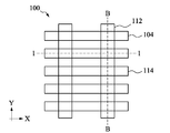
도 1a는 반도체 소자(또는 반도체 구조)(100)의 상면도이다. 도 1b는 도 1a의 B-B 선을 따라 취한 소자(100)의 단면도이다. 도 1a 및 도 1b를 참조하면, 소자(100)는 기판(102), 기판(102)으로부터 돌출한 복수의 핀(fin)(104), 기판(102) 위 및 상기 핀(104)들 사이의 격리 구조(106), 및 상기 핀(104)과 격리 구조(106) 위에 배치된 복수의 게이트 스택(112)을 포함한다. 각각의 게이트 스택(112)은 하이-k 유전체 층(108) 및 이 하이-k 유전체 층(108) 위의 도전성 층(110)을 포함한다. 도전성 층(110)은 하나 이상의 금속성 물질의 층을 포함한다. 그러므로 각각의 게이트 스택(112)은 하이-k 금속 게이트(또는 HK MG)(112)라고도 부른다. 게이트 스택(112)은 상기 하이-k 유전체 층(108) 아래에 계면층(도시 생략)을 또한 포함할 수 있다.1A is a top view of a semiconductor device (or semiconductor structure) 100. 1B is a cross-sectional view of the
상면도로 볼 때, 핀(104)은 X 방향을 따라 길게 배열되고, 게이트 스택(112)은 X 방향에 대략 수직인 Y 방향을 따라 길게 배열된다. 또한, 핀(104)들은 서로 대략 평행하고, 게이트 스택(112)은 서로 대략 평행하다. 소자(100)는 또한 X 방향을 따라 길게 배열되고 각각의 게이트 스택(112)을 적어도 2개의 부분으로 분리하는 유전체 층(114)을 포함한다. 게이트 스택(112)의 각 부분은 각각의 핀(104)과 결합하여 개별적인 핀펫(FinFET) 트랜지스터를 형성한다. 소자(100)는 게이트 스택(112) 및 유전체 층(114) 위에 배치된 하나 이상의 유전체 층(116)을 또한 포함한다. 소자(100)의 각 컴포넌트에 대해서는 뒤에서 자세히 설명한다.When viewed from a top view, the
기판(102)은 본 실시형태에서 실리콘 기판이다. 대안적으로, 기판(102)은 게르마늄과 같은 다른 기초 반도체; 실리콘 탄화물, 갈륨 비화물, 갈륨 인화물, 인듐 인화물, 인듐 비화물 및 인듐 안티몬화물을 포함한 화합물 반도체; 실리콘 게르마늄, 갈륨 비소 인화물, 알루미늄 인듐 인화물, 알루미늄 갈륨 비화물, 갈륨 인듐 비화물, 갈륨 인듐 인화물 및 갈륨 인듐 비소 인화물을 포함한 합금 반도체; 또는 이들의 조합을 포함할 수 있다.The
핀(104)은 실리콘, 게르마늄, 실리콘 탄화물, 갈륨 비화물, 갈륨 인화물, 인듐 인화물, 인듐 비화물, 인듐 안티몬화물, 실리콘 게르마늄, 갈륨 비소 인화물, 알루미늄 인듐 인화물, 알루미늄 갈륨 비화물, 갈륨 인듐 비화물, 갈륨 인듐 인화물 및 갈륨 인듐 비소 인화물과 같은 하나 이상의 반도체 물질을 포함할 수 있다. 일 실시형태에서, 핀(104)은 실리콘 층과 실리콘 게르마늄 층이 교대로 적층된 것과 같이 2개의 다른 반도체 물질이 교대로 적층된 층들을 포함할 수 있다. 핀(104)은 소자(100)의 성능을 개선하기 위한 도펀트를 추가로 포함할 수 있다. 예를 들면, 핀(104)은 인 또는 비소와 같은 n형 도펀트, 또는 붕소 또는 인듐과 같은 p형 도펀트를 포함할 수 있다.The
격리 구조(106)는 실리콘 산화물, 실리콘 질화물, 실리콘 산질화물, 플루오르 도핑 실리케이트 글라스(FSG), 로우-k 유전체 물질 및/또는 다른 적당한 절연 물질을 포함할 수 있다. 격리 구조(106)는 얕은 트렌치 격리(STI) 피쳐일 수 있다. 필드 산화물, 실리콘 국부 산화(LOCal Oxidation of Silicon, LOCOS), 및/또는 다른 적당한 구조와 같은 다른 격리 구조도 가능하다. 격리 구조(106)는 예를 들면 핀(104) 부근에 하나 이상의 열 산화물 라이너 층을 가진 다층 구조를 포함할 수 있다.
하이-k 유전체 층(108)은 하프늄 실리콘 산화물(HfSiO), 하프늄 산화물(HfO2), 알루미나(Al2O3), 지르콘 산화물(ZrO2), 란탄 산화물(La2O3), 티탄 산화물(TiO2), 이트륨 산화물(Y2O3), 스트론튬 티타네이트(SrTiO3) 또는 이들의 조합과 같은 하나 이상의 하이-k 유전체 물질(또는 하나 이상의 하이-k 유전체 물질 층)을 포함할 수 있다.The high-
도전성 층(110)은 일함수 금속 층, 도전성 장벽 층 및 금속 충전 층과 같은 하나 이상의 금속 층을 포함한다. 일함수 금속 층은 소자의 유형(PFET 또는 NFET)에 따라 p형 또는 n형 일함수 층일 수 있다. p형 일함수 층은 비제한적으로 티탄 질화물(TiN), 탄탈 질화물(TaN), 루테늄(Ru), 몰리브덴(Mo), 텅스텐(W), 백금(Pt) 또는 이들의 조합의 그룹으로부터 선택된 충분히 큰 유효 일함수를 가진 금속을 포함한다. n형 일함수 층은 비제한적으로 티탄(Ti), 알루미늄(Al), 탄탈 카바이드(TaC), 탄탈 카바이드 질화물(TaCN), 탄탈 실리콘 질화물(TaSiN), 티탄 실리콘 질화물(TiSiN) 또는 이들의 조합의 그룹으로부터 선택된 충분히 낮은 유효 일함수를 가진 금속을 포함한다. 금속 충전층은 알루미늄(Al), 텅스텐(W), 코발트(Co) 및/또는 다른 적당한 물질을 포함할 수 있다.The
유전체 층(114)은 실리콘 질화물, 실리콘 산화물, 실리콘 산질화물, 플루오르 도핑 실리케이트 글라스(FSG), 로우-k 유전체 물질 및/또는 다른 적당한 절연 물질과 같은 하나 이상의 유전체 물질을 포함할 수 있다. 특히, 게이트 스택(112)과 물리적으로 접촉하는 유전체 층(114)의 부분은 게이트 스택(112)의 금속 물질과 반응하지 않는 유전체 물질을 포함한다. 예를 들면, 유전체 층(114)의 상기 부분은 일 실시형태에서 실리콘 질화물을 포함한다.
유전체 층(116)은 실리콘 질화물, 실리콘 산화물, 실리콘 산질화물, 플루오르 도핑 실리케이트 글라스(FSG), 로우-k 유전체 물질 및/또는 다른 적당한 절연 물질과 같은 하나 이상의 유전체 물질을 포함할 수 있다.
도 1c를 참조하면서 소자(100)에 대하여 더 설명한다. 도 1c에서, 유전체 층(114, 116)은 절단 금속 게이트(CMG) 트렌치(113)의 세부를 설명하기 위해 생략하였다. 이 단면도에서, CMG 트렌치(113)는 게이트 스택(112)을 좌측 부분(112L)과 우측 부분(112R)으로 분리한다. 좌측 부분(112L)은 2개의 핀(104)과 맞물려서 하나의 트랜지스터를 형성하고, 우측 부분(112R)은 2개의 다른 핀(104)과 맞물려서 다른 하나의 트랜지스터를 형성한다. 각종 실시형태에서, 좌측(또는 우측) 부분은 임의 수의 핀(104)과 맞물려서 트랜지스터를 형성할 수 있다. 좌측 부분(112L)은 우측 부분(112R) 쪽으로 상부로부터 바닥부까지 경사진 측벽(SW1)을 갖는다. 측벽(SW1)은 기판(102)에 수직인 Z 방향과 각도(θ1)를 형성한다. 우측 부분(112R)은 좌측 부분(112L) 쪽으로 상부로부터 바닥부까지 경사진 측벽(SW2)을 갖는다. 측벽(SW2)은 Z 방향과 각도(θ2)를 형성한다. CMG 트렌치(113)는 게이트 스택(112)의 좌측 부분과 우측 부분이 서로로부터 완전히 격리되도록 격리 구조(106) 내로 연장한다. 게이트 스택(112)은 게이트 스택(112)과 격리 구조(106) 사이의 계면으로부터 게이트 스택(112)의 상부면까지 측정하였을 때 Z 방향을 따라 높이(H1)를 갖는다. CMG 트렌치(113)는 게이트 스택(112)의 상부면에 상부 개구를 갖고 게이트 스택(112)과 격리 구조(106) 사이의 계면에 바닥 개구를 갖는다. 상부 개구는 폭이 W1이고, 바닥 개구는 폭이 W2이다. CMG 트렌치(113)의 종횡비는 H1/W1으로 규정된다.The
일 실시형태에서, 높이(H1)은 80~140nm의 범위이고, 상부 개구 폭(W1)은 16~30nm의 범위일 수 있다. CMG 트렌치(113)의 종횡비는 3~10의 범위, 예를 들면 4~8 또는 5~7의 범위일 수 있다. 높은 종횡비에서, 만일 CMG 트렌치(113)가 수직 측벽을 가지면(전형적으로, 금속막의 건식 에칭에 의해 수직 측벽이 생성된다), 기존의 증착 기법으로는 전형적으로 깊고 좁은 트렌치의 바닥부에서 증착이 잘 안되기 때문에 유전체 층(114)으로 CMG 트렌치(113)를 완전하게 충전하는 것이 어렵다. 본 실시형태에서는 CMG 트렌치(113)가 테이퍼형 윤곽을 갖도록, 즉 W1>W2가 되도록 설계 및 가공된다. 실험에 의하면 그러한 테이퍼형 윤곽은 CMG 트렌치(113)에 대한 유전체 층(114)의 충전이 개선되는 것으로 나타났다.In one embodiment, the height H1 may range from 80 to 140 nm, and the upper opening width W1 may range from 16 to 30 nm. The aspect ratio of the
각종 실시형태에서, 각각의 각도(θ1, θ2)는 0°보다 크고(그래서 "경사진" 측벽임) tan-1(1/(2×AR))보다 작으며, 여기에서 AR은 본 실시형태에서 H1/W1과 동일한 CMG 트렌치(113)의 종횡비이다. 만일 2개의 각도(θ1, θ2)가 tan-1(1/(2×AR))과 같으면, CMG 트렌치(113)는 간신히 격리 구조(106)에 도달한다. 게이트 스택(112)의 좌측 부분과 우측 부분 간의 격리를 보장하기 위해, 2개의 각도(θ1, θ2)는 tan-1(1/(2×AR))보다 작게 되도록 설계된다. 일 실시형태에서, CMG 트렌치(113)는 각각의 각도(θ1, θ2)가 1~10°(또는 도)의 범위, 예를 들면 1.5~7° 또는 2~5°의 범위로 되도록 설계된다. 그러한 측벽 각은 높은 종횡비를 가진 CMG 트렌치(113)에 대한 유전체 물질(114)의 충전에 도움이 되고 효과적인 것으로 밝혀졌다. 실시형태에서, 상기 2개의 각도(θ1, θ2)는 서로 동일할 수도 있고 동일하지 않을 수도 있다.In various embodiments, each angle (θ1, θ2) is greater than 0° (so it is a “sloping” sidewall) and less than tan −1 (1/(2×AR)), where AR is the present embodiment It is the aspect ratio of the
일부 실시형태에서, W2/W1의 비는 유전체 층(114)(도 1b)이 게이트 스택(112)의 좌측 부분과 우측 부분을 완전하게 격리하고 측벽 각(θ1, θ2)이 막 증착을 용이하게 하기 위해 충분히 크게 되도록 0.4~0.8, 예를 들면 0.5~0.7이 되도록 설계된다. 실제로, 상기 측벽 각(θ1, θ2)은 W1, W2 및 H1의 값으로부터 도출될 수 있다.In some embodiments, the ratio of W2/W1 is that the dielectric layer 114 (FIG. 1B) completely isolates the left and right portions of the
도 2a 및 도 2b는 실시형태에 따른 반도체 소자(100)를 형성하는 방법(200)의 흐름도이다. 방법(200)은 단순히 예이고, 특허 청구범위에서 명시적으로 인용된 것 이상으로 본 발명을 제한하는 것으로 의도되지 않는다. 추가의 동작들이 방법(200)의 전, 중 및 후에 제공될 수 있고, 여기에서 설명하는 일부 동작들이 방법의 다른 실시형태에서는 교체, 제거 또는 이동될 수 있다. 방법(200)은 방법(200)에 따른 제조 단계 중에 반도체 소자(100)의 각종 단면도를 나타내는 도 3~12와 함께 이하에서 설명된다.2A and 2B are flowcharts of a
동작 202에서, 방법(200)(도 2a)은 도 3에 도시된 것처럼 기판(102), 기판(102)으로부터 돌출한 핀(104), 및 기판(102) 위 및 핀(104)들 사이의 격리 구조(106)를 가진 소자 구조(100)를 제공하거나 이러한 소자 구조(100)가 제공된다. 기판(102), 핀(104) 및 격리 구조(106)의 각종 물질은 도 1a~1c와 관련하여 위에서 설명하였다.In
일 실시형태에서, 기판(102)은 실리콘 웨이퍼와 같은 웨이퍼일 수 있다. 핀(104)은 기판(102)의 전체 면적 위에 하나 이상의 반도체 층을 에피택셜적으로 성장시키고, 그 다음에 개별적인 핀(104)을 형성하도록 패터닝함으로써 형성될 수 있다. 핀(104)은 임의의 적당한 방법에 의해 패터닝될 수 있다. 예를 들면, 핀(104)은 이중 패터닝 또는 다중 패터닝 공정을 포함한 하나 이상의 포토리소그래피 공정을 이용하여 패터닝될 수 있다. 일반적으로, 이중 패터닝 또는 다중 패터닝 공정은 포토리소그래피와 자기 정렬 공정을 결합하여 예를 들면 다른 경우에 단일의 직접 포토리소그래피 공정을 이용하여 획득할 수 있는 것보다 더 작은 피치를 가진 패턴을 생성할 수 있다. 예를 들면, 일 실시형태에서, 희생 층이 기판 위에 형성되고 포토리소그래피 공정을 이용하여 패터닝된다. 스페이서가 자기 정렬 공정을 이용하여 상기 패터닝된 희생 층과 나란하게 형성된다. 그 다음에 희생 층이 제거되고, 그 다음에 남아 있는 스페이서 또는 맨드렐을 이용하여 초기의 에피택셜 반도체 층을 에칭함으로써 핀(104)을 패터닝할 수 있다. 에칭 공정은 건식 에칭, 습식 에칭, 반응성 이온 에칭(RIE) 및/또는 다른 적당한 공정을 포함할 수 있다. 예를 들면, 건식 에칭 공정은 산소 함유 가스, 플루오르 함유 가스(예를 들면, CF4, CF6, CH2F2, CHF3 및/또는 C2F6), 염소 함유 가스(예를 들면, Cl2, CHCl3, CCl4 및/또는 BCl3), 브롬 함유 가스(예를 들면, HBr 및/또는 CHBr3), 요오드 함유 가스, 다른 적당한 가스 및/또는 플라즈마, 및/또는 이들의 조합으로 구현할 수 있다. 예를 들면, 습식 에칭 공정은 묽은 불화수소산(DHF); 수산화칼륨(KOH) 용액; 암모니아; 불화수소산(HF), 질산(HNO3) 및/또는 아세트산(CH3COOH)을 포함한 용액; 또는 다른 적당한 습식 에천트로의 에칭을 포함할 수 있다.In one embodiment, the
격리 영역(106)은 하나 이상의 증착 및 에칭 방법에 의해 형성될 수 있다. 증착 방법은 열 산화, 화학적 산화, 및 화학 기상 증착(CVD), 예를 들면 유동성 CVD(FCVD)를 포함할 수 있다. 에칭 방법은 건식 에칭, 습식 에칭 및 화학 기계 평탄화(CMP)를 포함할 수 있다.
동작 204에서, 방법(200)(도 2a)은 도 4a 및 도 4b에 도시된 것처럼 핀(104)과 맞물리는 더미(또는 임시) 게이트 구조를 형성한다. 도 4a는 도 1a의 1-1 선을 따라 취한 소자(100)의 단면도이고, 도 4b는 도 1a의 B-B 선을 따라 취한 소자(100)의 단면도이다. 도 4a 및 4b를 참조하면, 더미 게이트는 계면층(150), 전극층(152) 및 2개의 하드 마스크층(154, 156)을 포함한다. 동작 204는 더미 게이트 구조의 측벽 위에 게이트 스페이서(160)를 또한 형성한다.In
계면층(150)은 실리콘 산화물(예를 들면, SiO2) 또는 실리콘 산질화물(예를 들면, SiON)과 같은 유전체 물질을 포함하고, 화학적 산화, 열 산화, 원자층 증착(ALD), CVD 및/또는 다른 적당한 방법에 의해 형성될 수 있다. 게이트 전극(152)은 다결정 실리콘(폴리-Si)을 포함할 수 있고 저압 화학 기상 증착(LPCVD) 및 플라즈마 강화 CVD(PECVD)와 같은 적당한 증착 공정에 의해 형성될 수 있다. 각각의 하드 마스크 층(154, 156)은 실리콘 산화물 및/또는 실리콘 질화물과 같은 하나 이상의 유전체 물질 층을 포함할 수 있고 CVD 또는 다른 적당한 방법에 의해 형성될 수 있다. 각종 층(150, 152, 154, 156)은 포토리소그래피 및 에칭 공정에 의해 패터닝될 수 있다. 게이트 스페이서(160)는 실리콘 산화물, 실리콘 질화물, 실리콘 산질화물, 실리콘 탄화물, 다른 유전체 물질 또는 이들의 조합과 같은 유전체 물질을 포함할 수 있고, 하나 이상의 물질 층을 포함할 수 있다. 게이트 스페이서(160)는 격리 구조(106), 핀(104) 및 더미 게이트 구조(150/152/154/156) 위에 블랭킷으로서 스페이서 물질을 증착함으로써 형성될 수 있다. 그 다음에 상기 스페이서 물질은 격리 구조(106), 하드 마스크 층(156) 및 핀(104)의 상부면을 노출시키도록 이방성 에칭 공정에 의해 에칭된다. 더미 게이트 구조(150/152/154/156)의 측벽 위에 있는 스페이서 물질 부분은 게이트 스페이서(160)가 된다. 인근의 게이트 스페이서(160)는 소자(100)의 S/D 영역에서 핀(104)을 노출시키는 트렌치(158)를 제공한다.The
동작 206에서, 방법(200)(도 2a)은 도 1a의 1-1 선을 따라 취한 소자(100)의 단면도인 도 5에 도시된 것처럼 소스/드레인(또는 S/D) 피쳐(162), 콘택트 에칭 스톱 층(CESL)(164), 층간 유전체(ILD) 층(166) 및 이 ILD 층(166) 위의 보호 유전체 층(168)을 형성한다. 예를 들면, 동작 206은 트렌치(158) 내의 노출된 핀(104) 내로 리세스를 에칭하고, 리세스 내에 반도체 물질을 에피택셜적으로 성장시킬 수 있다. 반도체 물질은 도 5에 도시된 것처럼 핀(104)의 상부면 위로 상승할 수 있다. 동작 206은 NFET 및 PFET용의 S/D 피쳐(162)를 별도로 형성할 수 있다. 예를 들면, 동작 206은 NFET 용의 n형 도핑된 실리콘으로 또는 PFET용의 p형 도핑된 실리콘 게르마늄으로 S/D 피쳐(162)를 형성할 수 있다. 그 다음에, 동작 206은 S/D 피쳐(162) 위에 CESL(164) 및 ILD 층(166)을 증착할 수 있다. CESL(164)은 실리콘 질화물, 실리콘 산질화물, 산소(O) 또는 탄소(C) 원소가 있는 실리콘 질화물 및/또는 다른 물질을 포함할 수 있고, CVD, PVD(물리 기상 증착), ALD 또는 다른 적당한 방법에 의해 형성될 수 있다. ILD 층(166)은 테트라에틸오소실리케이트(TEOS) 산화물, 비도핑 실리케이트 글라스, 또는 보로포스포실리케이트 글라스(BPSG)와 같은 도핑된 실리콘 산화물, 용융 실리카 클라스(FSG), 포스포실리케이트 글라스(PSG), 붕소 도핑 실리콘 글라스(BSG), 및/또는 다른 적당한 유전체 물질을 포함할 수 있다. ILD 층(166)은 PECVD, FCVD 또는 다른 적당한 방법에 의해 형성될 수 있다. 계속하여, 동작 206은 ILD 층(166)을 에치백하고, 후속 에칭 공정 중에 ILD 층(166)을 보호하기 위해 실리콘 질화물과 같은 질화물을 포함할 수 있는 보호 유전체 층(168)을 증착할 수 있다. 동작 206은 소자(100)의 상부면을 평탄화하고, 하드 마스크 층(154, 156)을 제거하며, 유전체 층(152)을 노출시키기 위해 하나 이상의 CMP 공정을 수행한다.In
동작 208에서, 방법(200)(도 2a)은 도 6a와 도 6b에 도시된 것처럼 게이트 트렌치(169)를 형성하기 위해 더미 게이트 구조를 제거한다. 도 6a와 도 6b는 각각 도 1a의 1-1 선 및 B-B 선을 따라 취한 소자(100)의 단면도이다. 게이트 트렌치(169)는 핀(104)의 표면 및 게이트 스페이서(160)의 측벽 표면을 노출시킨다. 동작 208은 전극 층(152) 및 계면 층(150)의 물질에 대하여 선택적인 하나 이상의 에칭 공정을 포함할 수 있다. 에칭 공정은 건식 에칭, 습식 에칭, 반응성 이온 에칭 또는 다른 적당한 에칭 방법을 포함할 수 있다.In
동작 210에서, 방법(200)(도 2a)은 도 7a와 도 7b에 도시된 것처럼 게이트 트렌치(169) 내에 하이-k 금속 게이트(112)를 증착한다. 도 7a와 도 7b는 각각 도 1a의 1-1 선 및 B-B 선을 따라 취한 소자(100)의 단면도이다. 하이-k 금속 게이트(112)는 하이-k 유전체 층(108)과 도전성 층(110)을 포함한다. 하이-k 금속 게이트(112)는 하이-k 유전체 층(108)과 핀(104) 사이에 계면 층(예를 들면, SiO2)(도시 생략)을 또한 포함할 수 있다. 계면 층은 화학적 산화, 열 산화, 원자층 증착(ALD), 화학 기상 증착(CVD) 및/또는 다른 적당한 방법을 이용하여 형성될 수 있다. 하이-k 유전체 층(108) 및 도전성 층(110)의 물질은 도 1a~1c와 관련하여 위에서 설명하였다. 하이-k 유전체 층(108)은 하이-k 유전체 물질의 하나 이상의 층을 포함할 수 있고, CVD, ALD 및/또는 다른 적당한 방법을 이용하여 증착될 수 있다. 도전성 층(110)은 하나 이상의 일함수 금속 층 및 금속 충전 층을 포함할 수 있고, CVD, PVD, 도금 및/또는 다른 적당한 공정과 같은 방법을 이용하여 증착될 수 있다.In
동작 212에서, 방법(200)(도 2b)은 도 8에 도시된 것처럼 소자(100) 위에 하나 이상의 하드 마스크 층을 형성한다. 도 8은 이 제조 단계에서 도 1a의 B-B 선을 따라 취한 소자(100)의 단면도이다. 이 예에서는 2개의 하드 마스크 층(170, 172)이 도시되어 있다. 일 실시형태에서, 하드 마스크 층(170)은 티탄 질화물을 포함하고, 하드 마스크 층(172)은 실리콘 질화물을 포함한다. 본 실시형태에서, 하드 마스크 층(170)의 물질은 도전성 층(110)과 잘 접착하지만 도전성 층(110)과 반응하지 않는 물질로 선택된다. 하드 마스크 층(170, 172)은 CVD, PVD, ALD 또는 다른 적당한 방법을 이용하여 증착될 수 있다.In
동작 214에서, 방법(200)(도 2b)은 도 9에 도시된 것처럼 패턴화 하드 마스크를 형성하기 위해 상기 하나 이상의 하드 마스크 층을 패터닝한다. 도 9는 이 제조 단계에서 도 1a의 B-B 선을 따라 취한 소자(100)의 단면도이다. 도 9를 참조하면, 하드 마스크 층(170, 172)은 도전성 층(110)을 노출시키는 개구(113)를 제공하도록 패터닝(예를 들면, 에칭)된다. 일 예로서, 동작 214는 포토레지스트 코팅, 노광, 노광후 베이킹 및 현상에 의해 상기 하드 마스크 층(170, 172) 위에 패턴화 포토레지스트를 형성할 수 있다. 패턴화 포토레지스트는 도 1a의 유전체 층(114)의 패턴에 대응한다. 그 다음에, 동작 214는 개구(113)를 형성하기 위해 상기 패턴화 포토레지스트를 에칭 마스크로서 이용하여 상기 하드 마스크 층(170, 172)을 에칭한다. 에칭 공정은 습식 에칭, 건식 에칭, 반응성 이온 에칭 또는 다른 적당한 에칭 방법을 포함할 수 있다. 패턴화 포토레지스트는 그 다음에 예를 들면 레지스트 스트리핑에 의해 제거된다. 하드 마스크 층(170/172)에서 개구(113)의 측벽은 수직 또는 거의 수직이라는 점에 주목한다.In
동작 216에서, 방법(200)(도 2b)은 상기 개구(113)를 통하여 하이-k 금속 게이트(112)를 에칭한다. 패턴화 하드 마스크 층(170, 172)은 하이-k 금속 게이트(112)의 나머지를 에칭 공정으로부터 보호한다. 도 10을 참조하면, 동작 216은 개구(113)를 하이-k 금속 게이트(112)를 관통하여 하향으로 격리 구조(106) 내까지 연장시킨다. 특히, 동작 216은 도 1c와 관련하여 위에서 설명한 경사진 측벽(SW1, SW2)을 형성하도록 에칭 공정을 제어한다. 에칭 공정은 하이-k 금속 게이트(112) 내의 각종 층을 에칭하는 하나 이상의 에천트 또는 에천트들의 혼합물을 이용할 수 있다.In
예시적인 실시형태에서, 도전성 층(110)은 TiSiN, TaN, TiN, W 또는 이들의 조합을 포함한다. 이러한 도전성 층과 하이-k 유전체 층(108)을 에칭하기 위해, 동작 216은 염소, 플루오르, 브롬, 산소, 수소, 탄소 또는 이들의 조합의 원자들을 가진 에천트에 의한 건식 에칭 공정을 적용할 수 있다. 예를 들면, 에천트는 Cl2, O2, 탄소와 플루오르 함유 가스, 브롬과 플루오르 함유 가스, 및 탄소와 수소와 플루오르 함유 가스의 가스 혼합물을 가질 수 있다. 이러한 가스 혼합물에 의한 하이-k 금속 게이트(112)의 에칭은 에칭 공정 중에 CMG 트렌치(113)의 측벽 위에 일부 중합체(또는 중합체 물질)이 증착되게 하는 경향이 있다. 이러한 중합체는 측벽 쪽으로의 에칭을 느리게 하고, 이것에 의해 경사진 측벽(SW1, SW2)을 생성한다. 일 예로서, 에천트는 Cl2, O2, CF4, BCl3 및 CHF3의 가스 혼합물을 포함한다. 가스 혼합물의 BCl3의 양을 조정함으로써, 동작 216은 CMG 트렌치(113)의 측벽에 증착되는 BOxNy 중합체의 양을 제어할 수 있고, 이것에 의해 측벽(SW1, SW2)의 기울기를 제어한다. 예를 들면, 동작 216은 증착되는 BOxNy 중합체의 양을 증가시키기 위해 가스 혼합물에서 BCl3의 비율을 증가시킬 수 있다. 대안적으로 또는 추가적으로, 가스 혼합물의 CHF3의 양을 조정함으로써, 동작 216은 CMG 트렌치(113)의 측벽에 증착되는 TiFx 및 NFx 중합체의 양을 제어할 수 있고, 이것에 의해 측벽(SW1, SW2)의 기울기를 제어한다. 예를 들면, 동작 216은 증착되는 TiFx 및 NFx 중합체의 양을 증가시키기 위해 가스 혼합물에서 CHF3의 비율을 증가시킬 수 있다. 또한, 동작 216은 측벽(SW1, SW2)에 증착되는 CxFy 중합체의 양을 제어하기 위해 가스 혼합물에서 플루오르에 대한 탄소의 비율을 조정할 수 있다. 예를 들면, 동작 216은 CF4를 CxFy로 교체할 수 있고, 여기에서 x:y는 증착되는 CxFy 중합체의 양을 증가시키기 위해 1:4보다 크다(예를 들면, C4F6). 전술한 에천트 및 에칭 공정은 위에서 설명한 예시적인 물질 TiSiN, TaN, TiN 및 W로 제한되지 않고 상기 도전성 층(110) 및 하이-k 유전체 층(108)에 적합한 각종 물질에 적용될 수 있다. In an exemplary embodiment, the
더 나아가, 동작 216은 전술한 바와 같이 에천트를 제어하는 것에 추가적으로 또는 대안적으로 에칭 바이어스 전압을 또한 제어할 수 있다. (Z 방향을 따르는) 더 높은 에칭 바이어스 전압은 CMG 트렌치(113)에서 더 수직인 측벽을 생성하는 경향이 있고, 더 낮은 에칭 바이어스 전압은 에천트에 의한 하향 이온 충격을 감소시켜서 결과적으로 경사진 측벽을 생성한다. 본 실시형태에서, 동작 216은 50~100V 범위의 에칭 바이어스 전압을 인가할 수 있다. 또한, 동작 216은 본 실시형태에서 5~20mTorr의 압력, 100~200W의 에너지 및 75~125℃의 온도로 에칭 공정을 수행할 수 있다. 각종의 다른 값의 에칭 바이어스 전압, 에칭 압력, 에칭 에너지 및 에칭 온도도 가능하다. 또한, 게이트 스택(112)의 좌측 부분과 우측 부분 간의 격리를 보장하기 위해, 동작 216은 CMG 트렌치(113)를 격리 구조(106) 내로 연장시키기 위해 일부 오버에칭을 수행한다. 이러한 오버에칭은 기판(102)을 노출시키지 않도록 주의깊게 제어된다.Furthermore,
동작 218에서, 방법(200)(도 2b)은 도 11에 도시된 것처럼 유전체 층(114)을 형성하기 위해 하나 이상의 유전체 물질로 상기 CMG 트렌치(113)를 충전한다. 게이트 스택(112)의 측벽(도 10의 SW1, SW2)이 금속 물질을 내포하기 때문에, 유전체 층(114)의 적어도 외부(즉, 측벽(SW1, SW2)과 직접 접촉하는 부분)은 산소와 같은 활성 화학 성분이 없다. 본 실시형태에서, 유전체 층(114)의 외부는 실리콘 질화물을 포함하고, 산소 또는 산화물이 없다. 하이-k 유전체 층(108)이 산소를 포함하기 때문에, 일부 산소 성분은 궁극적으로 유전체 층(114)의 일부 내로 확산할 수 있다는 점에 주목한다. 그러나 이러한 확산된 산소는 일반적으로 유전체 층(114)의 하부로 제한된다. 유전체 층(114)은 일부 실시형태에서 그 내부에 일부 산화물을 포함할 수 있다. 대안적으로, 유전체 층(114)은 하나의 균일한 실리콘 질화물 층을 포함할 수 있고 산화물이 없다. 유전체 층(114)은 CVD, PVD, ALD 또는 다른 적당한 방법을 이용하여 증착될 수 있다. 본 실시형태에서, 유전체 층(114)은 CMG 트렌치(113)를 완전히 충전하기 위해 ALD를 이용하여 증착된다.At
동작 220에서, 방법(200)(도 2b)은 하나 이상의 CMP 공정을 수행하여 과잉 유전체 층(114)(CMG 트렌치(113)의 외측 부분) 및 하드 마스크 층(172, 170)을 제거한다. 일 실시형태에서, 하드 마스크 층(170)은 CMP 공정에 의해 하드 마스크 층(172)을 제거할 때 CMP 스톱으로서 소용된다. 다른 실시형태에서, 동작 220은 도전성 층(110)(뿐만 아니라 유전체 층(114))을 원하는 HK MG 높이까지 리세스할 수 있다. 결과적인 구조는 도 12에 도시하였다.In
동작 222에서, 방법(200)(도 2b)은 소자(100)의 제조를 완료하기 위한 추가의 단계들을 수행한다. 예를 들면, 방법(200)은 S/D 피쳐(162)(도 7a)와 게이트 스택(112)을 전기적으로 접속하는 콘택트 및 비아를 형성하고, 완전한 IC를 형성하기 위해 각종 트랜지스터를 접속하는 금속 상호접속을 형성할 수 있다.At
비록 제한하는 의도는 없지만, 본 발명의 하나 이상의 실시형태는 반도체 소자 및 그 형성에 많은 이익을 제공한다. 예를 들면, 본 발명의 실시형태들은 경사진 측벽을 가진 절단 금속 게이트 트렌치를 제공한다. 경사진 측벽은 종횡비가 높은 트렌치에 대한 유전체 물질의 충전을 개선한다. 이것은 소규모 소자의 경우에 특히 유용하다. 또한, 본 발명의 실시형태들은 기존의 반도체 제조 공정에 쉽게 통합될 수 있다.Although not intended to be limiting, one or more embodiments of the present invention provide many benefits to semiconductor devices and their formation. For example, embodiments of the present invention provide cut metal gate trenches with sloped sidewalls. Inclined sidewalls improve the filling of dielectric material for high aspect ratio trenches. This is particularly useful for small devices. Further, embodiments of the present invention can be easily integrated into an existing semiconductor manufacturing process.
예시적인 일 양태에 있어서, 본 발명은 반도체 소자와 관련된다. 소자는 기판과; 상기 기판으로부터 돌출하는 제1핀 및 제2핀과; 제1의 하이-k 금속 게이트(HK MG) 및 제2 HK MG를 포함하고, 상기 제1 HK MG는 상기 제1핀 위에 배치되고 상기 제2 HK MG는 상기 제2핀 위에 배치된다. 상면도로 볼 때, 상기 제1핀과 제2핀은 제1 방향을 따라 길게 배열되고, 상기 제1 및 제2 HK MG는 상기 제1 방향에 대략 수직인 제2 방향을 따라 길게 배열되며, 상기 제1 및 제2 HK MG는 상기 제2 방향을 따라 정렬된다. 상기 제2 방향을 따라 취한 단면도에서, 상기 제1 HK MG는 상기 제2 HK MG 쪽으로 상부로부터 바닥부까지 경사진 제1 측벽을 갖고, 상기 제2 HK MG는 상기 제1 HK MG 쪽으로 상부로부터 바닥부까지 경사진 제2 측벽을 갖는다.In one exemplary aspect, the present invention relates to a semiconductor device. The device includes a substrate; A first pin and a second pin protruding from the substrate; And a first high-k metal gate (HK MG) and a second HK MG, wherein the first HK MG is disposed on the first pin and the second HK MG is disposed on the second pin. When viewed from a top view, the first pin and the second pin are elongated along a first direction, and the first and second HK MG are elongated along a second direction substantially perpendicular to the first direction, and the The first and second HK MGs are aligned along the second direction. In the cross-sectional view taken along the second direction, the first HK MG has a first sidewall inclined from the top to the bottom toward the second HK MG, and the second HK MG has a bottom from the top toward the first HK MG It has a second side wall inclined to the negative.
소자의 일 실시형태에서, 상기 제1 측벽은 기판의 법선과 제1 각도를 형성하고, 상기 제1 각도는 1~10도의 범위 내에 있다. 추가의 실시형태에서, 상기 제1 각도는 2~5도의 범위 내에 있다. 다른 실시형태에서, 상기 제2 측벽은 기판의 법선과 제2 각도를 형성하고, 상기 제2 각도는 1~10도의 범위 내에 있다. 예를 들면, 상기 제2 각도는 2~5도의 범위 내에 있다.In one embodiment of the device, the first sidewall forms a first angle with a normal line of the substrate, and the first angle is in a range of 1 to 10 degrees. In a further embodiment, the first angle is in the range of 2-5 degrees. In another embodiment, the second sidewall forms a second angle with a normal line of the substrate, and the second angle is in the range of 1-10 degrees. For example, the second angle is in the range of 2 to 5 degrees.
일 실시형태에서, 소자는 상기 제1 측벽과 상기 제2 측벽 사이에서 측방향으로 유전체 물질을 또한 포함한다. 추가의 실시형태에서, 상기 유전체 물질은 상기 제1 측벽과 상기 제2 측벽 사이의 스페이스를 완전하게 충전한다.In one embodiment, the device also includes a dielectric material laterally between the first sidewall and the second sidewall. In a further embodiment, the dielectric material completely fills the space between the first sidewall and the second sidewall.
다른 실시형태에서, 제1 거리는 상기 제1 측벽의 상부와 상기 제2 측벽의 상부 사이이고, 제2 거리는 상기 제1 측벽의 바닥부와 상기 제2 측벽의 바닥부 사이이며, 상기 제1 거리에 대한 상기 제2 거리의 비율은 0.4~0.8의 범위이다. 추가의 실시형태에서, 상기 제1 거리에 대한 상기 제2 거리의 비율은 0.5~0.7의 범위이다.In another embodiment, the first distance is between the top of the first sidewall and the top of the second sidewall, the second distance is between the bottom of the first sidewall and the bottom of the second sidewall, and the first distance The ratio of the second distance to is in the range of 0.4 to 0.8. In a further embodiment, the ratio of the second distance to the first distance is in the range of 0.5-0.7.
소자의 일 실시형태에서, 상기 제1 측벽의 상부와 상기 제2 측벽의 상부 사이의 거리에 대한 상기 제1 HK MG의 높이의 비율은 3~10의 범위이다. 예를 들면, 상기 비율은 5~7의 범위이다. 또 다른 실시형태에서, 소자는 상기 제1핀과 상기 제2핀 사이 및 상기 제1 HK MG와 상기 제2 HK MG 아래에 격리 구조를 또한 포함한다.In one embodiment of the device, the ratio of the height of the first HK MG to the distance between the top of the first sidewall and the top of the second sidewall is in the range of 3-10. For example, the ratio is in the range of 5-7. In yet another embodiment, the device also includes an isolation structure between the first pin and the second pin and below the first HK MG and the second HK MG.
다른 하나의 예시적인 양태에 있어서, 본 발명은 반도체 소자와 관련된다. 소자는 기판과; 상기 기판으로부터 돌출하는 제1핀 및 제2핀과; 상기 기판으로부터 돌출하는 제3핀 및 제4핀과; 상기 제1핀 및 제2핀 위에 배치된 제1의 하이-k 금속 게이트(HK MG)와; 상기 제3핀 및 제4핀 위에 배치된 제2 HK MG를 포함한다. 상면도로 볼 때, 상기 제1핀, 제2핀, 제3핀 및 제4핀은 제1 방향을 따라 길게 배열되고, 상기 제1 및 제2 HK MG는 상기 제1 방향에 대략 수직인 제2 방향을 따라 길게 배열된다. 상기 제2 방향을 따라 취한 단면도에서, 상기 제1 HK MG는 제1 측벽을 갖고, 상기 제2 HK MG는 상기 제1 측벽의 대향측에 제2 측벽을 가지며, 상기 제1 및 제2 측벽은 기판의 법선과 2개의 각도를 형성하고, 각각의 각도는 tan-1(1/(2×AR))보다 작으며, 여기에서 AR은 상기 제1 측벽의 상부와 상기 제2 측벽의 상부 사이의 거리에 대한 상기 제1 HK MG의 높이의 비율이다. 상기 제1 측벽과 상기 제2 측벽 사이의 스페이스는 하나 이상의 유전체 물질에 의해 완전하게 점유된다. 일부 실시형태에서, 상기 2개의 각도는 각각 1.5~7도의 범위이다.In another exemplary aspect, the present invention relates to a semiconductor device. The device includes a substrate; A first pin and a second pin protruding from the substrate; A third pin and a fourth pin protruding from the substrate; A first high-k metal gate (HK MG) disposed on the first and second fins; And a second HK MG disposed on the third pin and the fourth pin. When viewed from a top view, the first pin, second pin, third pin, and fourth pin are elongated along a first direction, and the first and second HK MGs are a second pin substantially perpendicular to the first direction. It is arranged long along the direction. In a cross-sectional view taken along the second direction, the first HK MG has a first sidewall, the second HK MG has a second sidewall on an opposite side of the first sidewall, and the first and second sidewalls Two angles are formed with the normal of the substrate, each angle is less than tan -1 (1/(2×AR)), where AR is between the top of the first sidewall and the top of the second sidewall. It is the ratio of the height of the first HK MG to the distance. The space between the first sidewall and the second sidewall is completely occupied by one or more dielectric materials. In some embodiments, the two angles each range from 1.5 to 7 degrees.
소자의 일 실시형태에서, 단면도로 볼 때 제1 거리는 상기 제1 측벽의 상부와 상기 제2 측벽의 상부 사이이고, 제2 거리는 상기 제1 측벽의 바닥부와 상기 제2 측벽의 바닥부 사이이며, 상기 제1 거리에 대한 상기 제2 거리의 비율은 0.4~0.8의 범위이다. 소자의 다른 실시형태에서, 상기 AR은 4~8의 범위이다.In one embodiment of the device, when viewed in a cross-sectional view, a first distance is between an upper portion of the first sidewall and an upper portion of the second sidewall, and a second distance is between a bottom portion of the first sidewall and a bottom portion of the second sidewall. , The ratio of the second distance to the first distance is in the range of 0.4 to 0.8. In another embodiment of the device, the AR ranges from 4 to 8.
또 다른 양태에 있어서, 본 발명은 방법과 관련된다. 이 방법은 기판, 상기 기판으로부터 돌출하는 핀, 및 상기 기판 위 및 인접 핀들 사이에 격리 구조를 구비한 구조를 제공하는 단계를 포함하고, 상기 격리 구조는 상기 핀들보다 아래에 있다. 상기 방법은 상기 격리 구조 및 상기 핀들 위에 하이-k 유전체 층 및 도전성 층을 포함한 게이트를 형성하는 단계와; 상기 격리 구조를 노출시키도록 2개의 인접하는 핀들 사이의 게이트에 대해 에칭 공정을 수행하여 상기 게이트를 적어도 제1 부분과 제2 부분으로 분리하는 단계를 또한 포함한다. 상기 에칭 공정은 상기 제1 부분의 제1 측벽을 생성하고 대향측에 상기 제2 부분의 제2 측벽을 생성하도록 제어되며, 상기 제1 및 제2 측벽은 바닥 개구보다 더 넓은 상부 개구를 제공한다.In yet another aspect, the invention relates to a method. The method includes providing a structure having a substrate, a fin protruding from the substrate, and an isolation structure above the substrate and between adjacent fins, the isolation structure being below the fins. The method includes forming a gate including a high-k dielectric layer and a conductive layer over the isolation structure and the fins; Further comprising separating the gate into at least a first portion and a second portion by performing an etching process on the gate between two adjacent fins to expose the isolation structure. The etching process is controlled to create a first sidewall of the first portion and a second sidewall of the second portion on the opposite side, the first and second sidewalls providing an upper opening wider than the bottom opening .
방법의 일 실시형태에서, 상기 에칭 공정은 50~100V 범위의 바이어스 전압에 의한 건식 에칭을 포함하고, 방법의 일 실시형태에서 상기 도전성 층은 텅스텐(W)을 포함하고, 상기 에칭 공정은 CxFy를 함유한 가스 혼합물을 이용하며, 여기에서 x:y는 1:4보다 더 크다.In one embodiment of the method, the etching process includes dry etching with a bias voltage in the range of 50-100V, and in one embodiment of the method the conductive layer comprises tungsten (W), and the etching process is C x A gas mixture containing F y is used, where x:y is greater than 1:4.
방법의 일 실시형태에서, 상기 에칭 공정은 Cl2, O2, 탄소와 플루오르 함유 가스, 브롬과 플루오르 함유 가스, 및 탄소와 수소와 플루오르 함유 가스의 가스 혼합물에 의한 건식 에칭을 포함한다. 방법의 또 다른 실시형태에서, 상기 에칭 공정은 염소, 플루오르, 브롬, 산소, 수소 및 탄소의 원자들을 가진 에천트에 의한 건식 에칭을 포함한다.In one embodiment of the method, the etching process includes dry etching with a gas mixture of Cl 2 , O 2 , a gas containing carbon and fluorine, a gas containing bromine and fluorine, and a gas containing carbon and hydrogen and fluorine. In yet another embodiment of the method, the etching process includes dry etching with an etchant having atoms of chlorine, fluorine, bromine, oxygen, hydrogen and carbon.
지금까지 당업자가 본 발명의 각종 양태를 잘 이해할 수 있을 정도로 몇 가지 실시형태의 피쳐들을 설명하였다. 당업자라면 여기에서 소개한 실시형태의 동일한 목적을 실행하고 및/또는 동일한 장점을 달성하는 다른 공정 및 구조의 설계 또는 수정을 위한 기초로서 본 명세서의 설명을 쉽게 이용할 수 있다는 것을 인식할 것이다. 당업자라면 그러한 등가적인 구성이 본 발명의 정신 및 범위로부터 벗어나지 않는다는 점, 및 본 발명의 정신 및 범위로부터 벗어나지 않고 여기에서 설명한 실시형태의 각종 변경, 치환 및 개조가 가능하다는 점을 또한 인식할 것이다.The features of several embodiments have been described so far to the extent that those skilled in the art can better understand various aspects of the invention. Those skilled in the art will recognize that the description herein can be readily used as a basis for the design or modification of other processes and structures that perform the same objectives of the embodiments introduced herein and/or achieve the same advantages. Those skilled in the art will also recognize that such equivalent configurations do not depart from the spirit and scope of the present invention, and that various changes, substitutions and modifications of the embodiments described herein are possible without departing from the spirit and scope of the present invention.
<부기><Bookkeeping>
1. 반도체 소자에 있어서,1. In a semiconductor device,
기판과;A substrate;
상기 기판으로부터 돌출하는 제1핀 및 제2핀과;A first pin and a second pin protruding from the substrate;
제1 하이-k 금속 게이트(high-k metal gate, HK MG) 및 제2 HK MG- 상기 제1 HK MG는 상기 제1핀 위에 배치되고, 상기 제2 HK MG는 상기 제2핀 위에 배치됨 -A first high-k metal gate (HK MG) and a second HK MG- The first HK MG is disposed on the first pin, and the second HK MG is disposed on the second pin-
를 포함하고,Including,
상면도로 볼 때, 상기 제1핀과 상기 제2핀은 제1 방향을 따라 길게(lengthwise) 배열되고, 상기 제1 및 제2 HK MG는 상기 제1 방향에 수직인 제2 방향을 따라 길게 배열되며, 상기 제1 및 제2 HK MG는 상기 제2 방향을 따라 정렬되고,When viewed from a top view, the first pin and the second pin are arranged lengthwise along a first direction, and the first and second HK MG are arranged lengthwise along a second direction perpendicular to the first direction. And the first and second HK MG are aligned along the second direction,
상기 제2 방향을 따라 취한 단면도에서, 상기 제1 HK MG는 상기 제2 HK MG 를 향하여 상부로부터 바닥부까지 경사진 제1 측벽을 갖고, 상기 제2 HK MG는 상기 제1 HK MG를 향하여 상부로부터 바닥부까지 경사진 제2 측벽을 갖는 것인 반도체 소자.In a cross-sectional view taken along the second direction, the first HK MG has a first sidewall inclined from the top to the bottom toward the second HK MG, and the second HK MG is at the top toward the first HK MG A semiconductor device having a second sidewall inclined from the bottom to the bottom.
2. 제1항에 있어서, 상기 제1 측벽은 기판의 법선과 제1 각도를 형성하고, 상기 제1 각도는 1도~10도의 범위 내에 있는 것인 반도체 소자.2. The semiconductor device according to
3. 제2항에 있어서, 상기 제1 각도는 2도~5도의 범위 내에 있는 것인 반도체 소자.3. The semiconductor device according to claim 2, wherein the first angle is within a range of 2 degrees to 5 degrees.
4. 제2항에 있어서, 상기 제2 측벽은 기판의 법선과 제2 각도를 형성하고, 상기 제2 각도는 1도~10도의 범위 내에 있는 것인 반도체 소자.4. The semiconductor device according to claim 2, wherein the second sidewall forms a second angle with a normal line of the substrate, and the second angle is within a range of 1 to 10 degrees.
5. 제4항에 있어서, 상기 제2 각도는 2도~5도의 범위 내에 있는 것인 반도체 소자.5. The semiconductor device according to claim 4, wherein the second angle is within a range of 2 degrees to 5 degrees.
6. 제1항에 있어서, 상기 제1 측벽과 상기 제2 측벽 사이에서 측방향으로 유전체 물질을 더 포함한 반도체 소자.6. The semiconductor device of
7. 제6항에 있어서, 상기 유전체 물질은 상기 제1 측벽과 상기 제2 측벽 사이의 스페이스를 완전하게 충전하는 것인 반도체 소자.7. The semiconductor device of claim 6, wherein the dielectric material completely fills the space between the first sidewall and the second sidewall.
8. 제1항에 있어서, 상기 제1 측벽의 상부와 상기 제2 측벽의 상부 사이가 제1 거리이고, 상기 제1 측벽의 바닥부와 상기 제2 측벽의 바닥부 사이가 제2 거리이고, 상기 제1 거리에 대한 상기 제2 거리의 비율은 0.4~0.8의 범위인 것인 반도체 소자.8. The method of
9. 제8항에 있어서, 상기 제1 거리에 대한 상기 제2 거리의 비율은 0.5~0.7의 범위인 반도체 소자.9. The semiconductor device according to claim 8, wherein a ratio of the second distance to the first distance is in the range of 0.5 to 0.7.
10. 제1항에 있어서, 상기 제1 측벽의 상부와 상기 제2 측벽의 상부 사이의 거리에 대한 상기 제1 HK MG의 높이의 비율은 3~10의 범위인 반도체 소자.10. The semiconductor device of
11. 제10항에 있어서, 상기 비율은 5~7의 범위 반도체 소자.11. The semiconductor device according to claim 10, wherein the ratio is in the range of 5-7.
12. 제1항에 있어서, 상기 제1핀과 상기 제2핀 사이 및 상기 제1 HK MG와 상기 제2 HK MG 아래에 격리 구조를 더 포함한 반도체 소자.12. The semiconductor device of
13. 반도체 소자에 있어서,13. In a semiconductor device,
기판과;A substrate;
상기 기판으로부터 돌출하는 제1핀 및 제2핀과;A first pin and a second pin protruding from the substrate;
상기 기판으로부터 돌출하는 제3핀 및 제4핀과;A third pin and a fourth pin protruding from the substrate;
상기 제1핀 및 상기 제2핀 위에 배치된 제1 하이-k 금속 게이트(high-k metal gate, HK MG)와;A first high-k metal gate (HK MG) disposed on the first pin and the second pin;
상기 제3핀 및 상기 제4핀 위에 배치된 제2 HK MGA second HK MG disposed on the third pin and the fourth pin
를 포함하고,Including,
상면도로 볼 때, 상기 제1핀, 상기 제2핀, 상기 제3핀 및 상기 제4핀은 제1 방향을 따라 길게 배열되고, 상기 제1 및 제2 HK MG는 상기 제1 방향에 수직인 제2 방향을 따라 길게 정렬되며,When viewed from a top view, the first pin, the second pin, the third pin, and the fourth pin are elongated along a first direction, and the first and second HK MGs are perpendicular to the first direction. It is aligned long along the second direction,
상기 제2 방향을 따라 취한 단면도에서, 상기 제1 HK MG는 제1 측벽을 갖고, 상기 제2 HK MG는 상기 제1 측벽의 대향측에 제2 측벽을 가지며, 상기 제1 및 제2 측벽은 기판의 법선과 2개의 각도를 형성하고, 각각의 각도는 tan-1(1/(2×AR))보다 작으며, 여기에서 AR은 상기 제1 측벽의 상부와 상기 제2 측벽의 상부 사이의 거리에 대한 상기 제1 HK MG의 높이의 비율이고,In a cross-sectional view taken along the second direction, the first HK MG has a first sidewall, the second HK MG has a second sidewall on an opposite side of the first sidewall, and the first and second sidewalls Two angles are formed with the normal of the substrate, each angle is less than tan -1 (1/(2×AR)), where AR is between the top of the first sidewall and the top of the second sidewall. Is the ratio of the height of the first HK MG to the distance,
상기 제1 측벽과 상기 제2 측벽 사이의 스페이스는 하나 이상의 유전체 물질에 의해 완전하게 점유된 것인 반도체 소자.The semiconductor device wherein the space between the first sidewall and the second sidewall is completely occupied by one or more dielectric materials.
14. 제13항에 있어서, 단면도로 볼 때, 상기 제1 측벽의 상부와 상기 제2 측벽의 상부 사이가 제1 거리이고, 상기 제1 측벽의 바닥부와 상기 제2 측벽의 바닥부 사이가 제2 거리이고, 상기 제1 거리에 대한 상기 제2 거리의 비율은 0.4~0.8의 범위인 반도체 소자.14. The method of claim 13, wherein when viewed in a cross-sectional view, a first distance is between an upper portion of the first sidewall and an upper portion of the second sidewall, and a lower portion of the first sidewall and a bottom portion of the second sidewall are A second distance, and a ratio of the second distance to the first distance is in the range of 0.4 to 0.8.
15. 제13항에 있어서, 상기 AR은 4~8의 범위인 반도체 소자.15. The semiconductor device according to claim 13, wherein the AR is in the range of 4 to 8.
16. 방법에 있어서,16. In the method,
기판, 상기 기판으로부터 돌출하는 핀들, 및 상기 기판 위 및 인접 핀들 사이의 격리 구조- 상기 격리 구조는 상기 핀들보다 아래에 있음 -를 구비한 구조를 제공하는 단계와;Providing a structure having a substrate, pins protruding from the substrate, and an isolation structure between the pins above and adjacent to the substrate, the isolation structure being below the pins;
상기 격리 구조 및 상기 핀들 위에 하이-k 유전체 층 및 도전성 층을 포함한 게이트를 형성하는 단계와;Forming a gate including a high-k dielectric layer and a conductive layer over the isolation structure and the fins;
상기 격리 구조를 노출시키도록 2개의 인접하는 핀들 사이의 게이트에 에칭 공정을 수행하여, 상기 게이트를 적어도 제1 부분과 제2 부분으로 분리하는 단계Separating the gate into at least a first portion and a second portion by performing an etching process on a gate between two adjacent fins to expose the isolation structure
를 포함하고, 상기 에칭 공정은, 상기 제1 부분의 제1 측벽 및 대향측에 상기 제2 부분의 제2 측벽을 생성하도록 제어되며, 상기 제1 및 제2 측벽은 바닥 개구보다 더 넓은 상부 개구를 제공하는 것인 방법.Including, the etching process is controlled to generate a second sidewall of the second portion on the first sidewall and the opposite side of the first portion, the first and second sidewalls are upper openings wider than the bottom opening The method of providing.
17. 제16항에 있어서, 상기 에칭 공정은 50V~100V 범위의 바이어스 전압에 의한 건식 에칭을 포함한 것인 방법.17. The method of clause 16, wherein the etching process comprises dry etching with a bias voltage ranging from 50V to 100V.
18. 제16항에 있어서, 상기 도전성 층은 텅스텐(W)을 포함하고, 상기 에칭 공정은 CxFy를 함유한 가스 혼합물을 이용하며, 여기에서 x:y는 1:4보다 더 큰 것인 방법.18. The method of clause 16, wherein the conductive layer comprises tungsten (W), and the etching process uses a gas mixture containing C x F y , wherein x:y is greater than 1:4. Way.
19. 제16항에 있어서, 상기 에칭 공정은 Cl2, O2, 탄소와 플루오르 함유 가스, 브롬과 플루오르 함유 가스, 및 탄소와 수소와 플루오르 함유 가스의 가스 혼합물에 의한 건식 에칭을 포함한 것인 방법.19. The method of clause 16, wherein the etching process comprises dry etching with a gas mixture of Cl 2 , O 2 , a gas containing carbon and fluorine, a gas containing bromine and fluorine, and a gas containing carbon and hydrogen and fluorine. .
20. 제16항에 있어서, 상기 에칭 공정은 염소, 플루오르, 브롬, 산소, 수소 및 탄소의 원자들을 가진 에천트에 의한 건식 에칭을 포함한 것인 방법.20. The method of clause 16, wherein the etching process comprises dry etching with an etchant having atoms of chlorine, fluorine, bromine, oxygen, hydrogen and carbon.
Claims (10)
기판;
상기 기판으로부터 돌출하는 제1 핀 및 제2 핀;
제1 하이-k 금속 게이트(high-k metal gate, HK MG) 및 제2 HK MG - 상기 제1 HK MG는 상기 제1 핀 위에 배치되고, 상기 제2 HK MG는 상기 제2 핀 위에 배치되며, 상기 제1 및 제2 HK MG 각각은 도전성 층 및 하이-k 유전체 층을 포함하며,
상면도에서, 상기 제1 핀과 상기 제2 핀은 제1 방향을 따라 종방향으로(lengthwise) 배열되고, 상기 제1 및 제2 HK MG는 상기 제1 방향에 수직인 제2 방향을 따라 종방향으로 배열되며, 상기 제1 및 제2 HK MG는 상기 제2 방향을 따라 정렬되고,
상기 제2 방향을 따라 취한 단면도에서, 상기 제1 HK MG의 상기 도전성 층은 상기 제2 HK MG 를 향하여 상부에서 바닥부로 경사진 제1 측벽을 갖고, 상기 제2 HK MG의 상기 도전성 층은 상기 제1 HK MG를 향하여 상부에서 바닥부로 경사진 제2 측벽을 가짐 - ;
상기 제1 및 제2 측벽 상의 중합체; 및
상기 제1 측벽 상의 중합체와 상기 제2 측벽 상의 중합체 사이에 측방향(laterally)으로 있는 유전체 재료
를 포함하는 반도체 디바이스.In a semiconductor device,
Board;
A first fin and a second fin protruding from the substrate;
A first high-k metal gate (HK MG) and a second HK MG-the first HK MG is disposed on the first fin, the second HK MG is disposed on the second fin, , Each of the first and second HK MG includes a conductive layer and a high-k dielectric layer,
In the top view, the first pin and the second pin are arranged lengthwise along a first direction, and the first and second HK MG are longitudinally aligned along a second direction perpendicular to the first direction. Are arranged in a direction, and the first and second HK MG are aligned along the second direction,
In a cross-sectional view taken along the second direction, the conductive layer of the first HK MG has a first sidewall inclined from the top to the bottom toward the second HK MG, and the conductive layer of the second HK MG is It has a second sidewall inclined from the top to the bottom towards the 1st HK MG-;
Polymers on the first and second sidewalls; And
A dielectric material laterally between the polymer on the first sidewall and the polymer on the second sidewall
A semiconductor device comprising a.
기판;
상기 기판으로부터 돌출하는 제1 핀 및 제2 핀;
상기 기판으로부터 돌출하는 제3 핀 및 제4 핀;
상기 제1 핀 및 상기 제2 핀 위에 배치된 제1 하이-k 금속 게이트(high-k metal gate, HK MG); 및
상기 제3 핀 및 상기 제4 핀 위에 배치된 제2 HK MG
를 포함하고,
상기 제1 및 제2 HK MG 각각은 도전성 층 및 하이-k 유전체 층을 포함하며,
상면도에서, 상기 제1 핀, 상기 제2 핀, 상기 제3 핀 및 상기 제4 핀은 제1 방향을 따라 종방향으로(lengthwise) 배열되고, 상기 제1 및 제2 HK MG는 상기 제1 방향에 수직인 제2 방향을 따라 종방향으로 정렬되며,
상기 제2 방향을 따라 취한 단면도에서, 상기 제1 HK MG의 도전성 층은 제1 측벽을 갖고, 상기 제2 HK MG의 도전성 층은 상기 제1 측벽에 대향하는 제2 측벽을 가지며, 상기 제1 및 제2 측벽은 기판의 법선과 2개의 각도를 형성하고, 각각의 각도는 tan-1(1/(2×AR))보다 작으며, 여기에서 AR은 상기 제1 측벽의 상부와 상기 제2 측벽의 상부 사이의 거리에 대한 상기 제1 HK MG의 높이의 비율이고,
상기 제1 측벽과 상기 제2 측벽 사이의 스페이스는 상기 제1 및 제2 HK MG의 하이-k 유전체 층과 상이한 하나 이상의 유전체 물질과 중합체에 의해 완전하게 점유된 것인 반도체 디바이스.In a semiconductor device,
Board;
A first fin and a second fin protruding from the substrate;
A third pin and a fourth pin protruding from the substrate;
A first high-k metal gate (HK MG) disposed on the first fin and the second fin; And
A second HK MG disposed on the third pin and the fourth pin
Including,
Each of the first and second HK MG includes a conductive layer and a high-k dielectric layer,
In the top view, the first pin, the second pin, the third pin, and the fourth pin are arranged lengthwise along a first direction, and the first and second HK MGs are the first Aligned longitudinally along a second direction perpendicular to the direction,
In the cross-sectional view taken along the second direction, the conductive layer of the first HK MG has a first sidewall, the conductive layer of the second HK MG has a second sidewall facing the first sidewall, and the first And the second sidewall forms two angles with the normal line of the substrate, each angle being less than tan -1 (1/(2×AR)), where AR is an upper portion of the first sidewall and the second Is the ratio of the height of the first HK MG to the distance between the top of the sidewall,
Wherein the space between the first sidewall and the second sidewall is completely occupied by one or more dielectric materials and polymers different from the high-k dielectric layers of the first and second HK MG.
기판, 상기 기판으로부터 돌출하는 핀들, 및 상기 기판 위 그리고 인접 핀들 사이의 격리 구조 - 상기 격리 구조는 상기 핀들보다 아래에 있음 - 를 갖는 구조체를 제공하는 단계;
상기 격리 구조 및 상기 핀들 위에 하이-k 유전체 층 및 도전성 층을 포함하는 게이트를 형성하는 단계; 및
상기 격리 구조를 노출시키도록 2개의 인접하는 핀들 사이의 게이트에 에칭 공정을 수행하여, 상기 게이트를 적어도 제1 부분과 제2 부분으로 분리하는 단계
를 포함하고,
상기 에칭 공정은, 상기 제1 부분의 제1 측벽 및 상기 제2 부분의 대향하는 제2 측벽을 생성하도록 상기 제1 부분의 제1 측벽 및 상기 제2 부분의 제2 측벽 상에 증착되는 중합체에 의해 제어되며, 상기 제1 및 제2 측벽은 바닥 개구보다 더 넓은 상부 개구를 제공하고, 상기 제1 측벽과 상기 제2 측벽 사이의 스페이스는 상기 게이트의 하이-k 유전체 층과 상이한 하나 이상의 유전체 물질과 중합체에 의해 완전하게 점유된 것인 방법.In the way,
Providing a structure having a substrate, fins protruding from the substrate, and an isolation structure above the substrate and between adjacent fins, the isolation structure being below the fins;
Forming a gate including a high-k dielectric layer and a conductive layer over the isolation structure and the fins; And
Separating the gate into at least a first portion and a second portion by performing an etching process on a gate between two adjacent fins to expose the isolation structure
Including,
The etching process includes a polymer deposited on the first sidewall of the first portion and the second sidewall of the second portion to create a first sidewall of the first portion and an opposing second sidewall of the second portion. Wherein the first and second sidewalls provide an upper opening wider than the bottom opening, and the space between the first sidewall and the second sidewall is at least one dielectric material different from the high-k dielectric layer of the gate. And completely occupied by the polymer.
Applications Claiming Priority (4)
| Application Number | Priority Date | Filing Date | Title |
|---|---|---|---|
| US201762551903P | 2017-08-30 | 2017-08-30 | |
| US62/551,903 | 2017-08-30 | ||
| US15/904,835 US10535654B2 (en) | 2017-08-30 | 2018-02-26 | Cut metal gate with slanted sidewalls |
| US15/904,835 | 2018-02-26 |
Publications (2)
| Publication Number | Publication Date |
|---|---|
| KR20190024626A KR20190024626A (en) | 2019-03-08 |
| KR102169642B1 true KR102169642B1 (en) | 2020-10-23 |
Family
ID=65437569
Family Applications (1)
| Application Number | Title | Priority Date | Filing Date |
|---|---|---|---|
| KR1020180061279A KR102169642B1 (en) | 2017-08-30 | 2018-05-29 | Cut metal gate with slanted sidewalls |
Country Status (4)
| Country | Link |
|---|---|
| US (2) | US10535654B2 (en) |
| KR (1) | KR102169642B1 (en) |
| CN (1) | CN109427777B (en) |
| TW (1) | TWI692104B (en) |
Families Citing this family (22)
| Publication number | Priority date | Publication date | Assignee | Title |
|---|---|---|---|---|
| CN109585293B (en) * | 2017-09-29 | 2021-12-24 | 台湾积体电路制造股份有限公司 | Footing removal in metal cutting processes |
| US10483369B2 (en) * | 2017-10-30 | 2019-11-19 | Globalfoundries Inc. | Methods of forming replacement gate structures on transistor devices |
| US10629492B2 (en) | 2018-04-27 | 2020-04-21 | Taiwan Semiconductor Manufacturing Co., Ltd. | Gate structure having a dielectric gate and methods thereof |
| US11398477B2 (en) | 2019-05-29 | 2022-07-26 | Taiwan Semiconductor Manufacturing Company, Ltd. | Semiconductor device and method |
| US10854603B2 (en) | 2018-06-29 | 2020-12-01 | Taiwan Semiconductor Manufacturing Company, Ltd. | Semiconductor device and method |
| CN111341847B (en) * | 2018-12-19 | 2023-03-28 | 联华电子股份有限公司 | Semiconductor structure and manufacturing method thereof |
| US11164866B2 (en) * | 2019-02-20 | 2021-11-02 | Taiwan Semiconductor Manufacturing Co., Ltd. | Semiconductor structure and method for manufacturing the same |
| US11043595B2 (en) | 2019-06-14 | 2021-06-22 | Taiwan Semiconductor Manufacturing Co., Ltd. | Cut metal gate in memory macro edge and middle strap |
| US11211116B2 (en) | 2019-09-27 | 2021-12-28 | Taiwan Semiconductor Manufacturing Co., Ltd. | Embedded SRAM write assist circuit |
| CN110752152B (en) * | 2019-10-17 | 2021-10-15 | 上海华力集成电路制造有限公司 | Process method for cutting off polysilicon gate of fin transistor |
| US12002715B2 (en) | 2019-10-29 | 2024-06-04 | Taiwan Semiconductor Manufacturing Co., Ltd. | Semiconductor device and method |
| DE102020119461B4 (en) | 2019-10-29 | 2024-11-14 | Taiwan Semiconductor Manufacturing Co., Ltd. | SEMICONDUCTOR DEVICE AND METHOD |
| US11482421B2 (en) * | 2019-10-29 | 2022-10-25 | Taiwan Semiconductor Manufacturing Co., Ltd. | Method of forming a semiconductor device by a replacement gate process |
| US12009266B2 (en) * | 2019-12-18 | 2024-06-11 | Taiwan Semiconductor Manufacturing Co., Ltd. | Structure for fringing capacitance control |
| US11508847B2 (en) * | 2020-03-09 | 2022-11-22 | Intel Corporation | Transistor arrangements with metal gate cuts and recessed power rails |
| US11121138B1 (en) | 2020-04-24 | 2021-09-14 | Taiwan Semiconductor Manufacturing Co., Ltd. | Low resistance pickup cells for SRAM |
| US11374088B2 (en) | 2020-08-14 | 2022-06-28 | Taiwan Semiconductor Manufacturing Co., Ltd. | Leakage reduction in gate-all-around devices |
| US12094822B2 (en) | 2020-11-17 | 2024-09-17 | Intel Corporation | Buried power rails with self-aligned vias to trench contacts |
| US11670681B2 (en) | 2021-01-14 | 2023-06-06 | Taiwan Semiconductor Manufacturing Company, Ltd. | Method of forming fully strained channels |
| US11482518B2 (en) | 2021-03-26 | 2022-10-25 | Taiwan Semiconductor Manufacturing Co., Ltd. | Semiconductor structures having wells with protruding sections for pickup cells |
| US20240105453A1 (en) * | 2022-09-27 | 2024-03-28 | Intel Corporation | High aspect ratio metal gate cuts |
| US20240222447A1 (en) * | 2022-12-28 | 2024-07-04 | Intel Corporation | Gate cut, and source and drain contacts |
Family Cites Families (27)
| Publication number | Priority date | Publication date | Assignee | Title |
|---|---|---|---|---|
| EP0023429B1 (en) | 1979-07-31 | 1985-12-18 | Fujitsu Limited | Dry etching of metal film |
| JPH0622218B2 (en) | 1988-08-06 | 1994-03-23 | 富士通株式会社 | Etching method |
| CN102347227B (en) * | 2010-07-30 | 2013-08-14 | 中芯国际集成电路制造(上海)有限公司 | Metal gate formation method |
| CN102487039A (en) * | 2010-12-03 | 2012-06-06 | 中芯国际集成电路制造(上海)有限公司 | Preparation method of semiconductor device |
| KR20120089513A (en) * | 2010-12-13 | 2012-08-13 | 삼성전자주식회사 | Non-volatile memory devices and methods of fabricating the same |
| US8598675B2 (en) * | 2011-02-10 | 2013-12-03 | Taiwan Semiconductor Manufacturing Company, Ltd. | Isolation structure profile for gap filling |
| US8816444B2 (en) | 2011-04-29 | 2014-08-26 | Taiwan Semiconductor Manufacturing Company, Ltd. | System and methods for converting planar design to FinFET design |
| CN103117213B (en) * | 2011-11-16 | 2015-10-07 | 中芯国际集成电路制造(上海)有限公司 | Method for forming metallic grid |
| US9236267B2 (en) | 2012-02-09 | 2016-01-12 | Taiwan Semiconductor Manufacturing Company, Ltd. | Cut-mask patterning process for fin-like field effect transistor (FinFET) device |
| US8785285B2 (en) | 2012-03-08 | 2014-07-22 | Taiwan Semiconductor Manufacturing Company, Ltd. | Semiconductor devices and methods of manufacture thereof |
| US8860148B2 (en) | 2012-04-11 | 2014-10-14 | Taiwan Semiconductor Manufacturing Company, Ltd. | Structure and method for FinFET integrated with capacitor |
| US9105490B2 (en) | 2012-09-27 | 2015-08-11 | Taiwan Semiconductor Manufacturing Company, Ltd. | Contact structure of semiconductor device |
| US8823065B2 (en) | 2012-11-08 | 2014-09-02 | Taiwan Semiconductor Manufacturing Company, Ltd. | Contact structure of semiconductor device |
| US8772109B2 (en) | 2012-10-24 | 2014-07-08 | Taiwan Semiconductor Manufacturing Company, Ltd. | Apparatus and method for forming semiconductor contacts |
| US9236300B2 (en) | 2012-11-30 | 2016-01-12 | Taiwan Semiconductor Manufacturing Company, Ltd. | Contact plugs in SRAM cells and the method of forming the same |
| US8980763B2 (en) | 2012-11-30 | 2015-03-17 | Applied Materials, Inc. | Dry-etch for selective tungsten removal |
| CN104347477B (en) * | 2013-07-24 | 2018-06-01 | 中芯国际集成电路制造(上海)有限公司 | The forming method of semiconductor structure |
| US9136106B2 (en) | 2013-12-19 | 2015-09-15 | Taiwan Semiconductor Manufacturing Company, Ltd. | Method for integrated circuit patterning |
| US9331074B1 (en) * | 2015-01-30 | 2016-05-03 | Taiwan Semiconductor Manufacturing Co., Ltd. | Semiconductor device and manufacturing method thereof |
| TWI652824B (en) * | 2015-04-13 | 2019-03-01 | 聯華電子股份有限公司 | Semiconductor structure and process thereof |
| US9559205B2 (en) * | 2015-05-29 | 2017-01-31 | Taiwan Semiconductor Manufacturing Company, Ltd. | Structure and formation method of semiconductor device structure |
| CN105244320A (en) * | 2015-08-28 | 2016-01-13 | 西安电子科技大学 | SOI-based CMOS integrated device with strain Ge channel and inverted trapezoidal grid and preparation method of integrated device |
| US9659930B1 (en) * | 2015-11-04 | 2017-05-23 | Taiwan Semiconductor Manufacturing Co., Ltd. | Semiconductor device and manufacturing method thereof |
| US9520482B1 (en) | 2015-11-13 | 2016-12-13 | Taiwan Semiconductor Manufacturing Company, Ltd. | Method of cutting metal gate |
| US9773912B2 (en) * | 2016-01-28 | 2017-09-26 | Taiwan Semiconductor Manufacturing Company Limited | Semiconductor device and manufacturing method thereof |
| US9627379B1 (en) * | 2016-03-07 | 2017-04-18 | Taiwan Semiconductor Manufacturing Co., Ltd. | FinFET devices and methods of forming the same |
| US10032632B2 (en) * | 2016-10-04 | 2018-07-24 | International Business Machines Corporation | Selective gas etching for self-aligned pattern transfer |
-
2018
- 2018-02-26 US US15/904,835 patent/US10535654B2/en active Active
- 2018-05-25 CN CN201810513503.7A patent/CN109427777B/en active Active
- 2018-05-29 KR KR1020180061279A patent/KR102169642B1/en active IP Right Grant
- 2018-06-20 TW TW107121167A patent/TWI692104B/en active
- 2018-11-19 US US16/195,258 patent/US11616061B2/en active Active
Also Published As
| Publication number | Publication date |
|---|---|
| TW201914025A (en) | 2019-04-01 |
| US20190088650A1 (en) | 2019-03-21 |
| KR20190024626A (en) | 2019-03-08 |
| US11616061B2 (en) | 2023-03-28 |
| CN109427777A (en) | 2019-03-05 |
| CN109427777B (en) | 2021-08-24 |
| US10535654B2 (en) | 2020-01-14 |
| US20190067277A1 (en) | 2019-02-28 |
| TWI692104B (en) | 2020-04-21 |
Similar Documents
| Publication | Publication Date | Title |
|---|---|---|
| KR102169642B1 (en) | Cut metal gate with slanted sidewalls | |
| US11721544B2 (en) | Cut metal gate process for reducing transistor spacing | |
| US11694931B2 (en) | Metal gate structure cutting process | |
| US10978350B2 (en) | Structure and method for metal gates with roughened barrier layer | |
| US11948842B2 (en) | Etch stop layer between substrate and isolation structure | |
| CN110176443B (en) | Bimetallic through hole for reducing contact resistance | |
| TW202017189A (en) | Semiconductor device | |
| CN110648919A (en) | Gate structure fabrication with notches | |
| US20230352345A1 (en) | Metal gate structure cutting process | |
| US10950434B2 (en) | Methods of reducing gate spacer loss during semiconductor manufacturing |
Legal Events
| Date | Code | Title | Description |
|---|---|---|---|
| A201 | Request for examination | ||
| E902 | Notification of reason for refusal | ||
| E90F | Notification of reason for final refusal | ||
| E701 | Decision to grant or registration of patent right |