JP4996323B2 - Two-dimensional digital data acquisition element and holographic storage device - Google Patents
Two-dimensional digital data acquisition element and holographic storage device Download PDFInfo
- Publication number
- JP4996323B2 JP4996323B2 JP2007119437A JP2007119437A JP4996323B2 JP 4996323 B2 JP4996323 B2 JP 4996323B2 JP 2007119437 A JP2007119437 A JP 2007119437A JP 2007119437 A JP2007119437 A JP 2007119437A JP 4996323 B2 JP4996323 B2 JP 4996323B2
- Authority
- JP
- Japan
- Prior art keywords
- digital data
- dimensional digital
- output
- circuit
- data acquisition
- Prior art date
- Legal status (The legal status is an assumption and is not a legal conclusion. Google has not performed a legal analysis and makes no representation as to the accuracy of the status listed.)
- Expired - Fee Related
Links
- 238000003860 storage Methods 0.000 title claims description 20
- 230000015654 memory Effects 0.000 claims description 38
- 230000003287 optical effect Effects 0.000 claims description 36
- 238000001514 detection method Methods 0.000 claims description 20
- 238000006243 chemical reaction Methods 0.000 claims description 18
- 238000004364 calculation method Methods 0.000 claims description 5
- 239000011159 matrix material Substances 0.000 claims description 5
- 230000003321 amplification Effects 0.000 claims description 4
- 238000003199 nucleic acid amplification method Methods 0.000 claims description 4
- 230000001934 delay Effects 0.000 claims description 2
- 230000001678 irradiating effect Effects 0.000 claims 1
- 238000010586 diagram Methods 0.000 description 24
- 230000007547 defect Effects 0.000 description 18
- 238000000034 method Methods 0.000 description 15
- 230000000875 corresponding effect Effects 0.000 description 9
- 230000008569 process Effects 0.000 description 5
- 239000000758 substrate Substances 0.000 description 5
- 230000004075 alteration Effects 0.000 description 4
- 230000008859 change Effects 0.000 description 4
- 238000003384 imaging method Methods 0.000 description 4
- 230000001276 controlling effect Effects 0.000 description 3
- 230000000694 effects Effects 0.000 description 3
- 238000004519 manufacturing process Methods 0.000 description 3
- 230000005540 biological transmission Effects 0.000 description 2
- 238000013500 data storage Methods 0.000 description 2
- 230000006870 function Effects 0.000 description 2
- 239000012535 impurity Substances 0.000 description 2
- 230000009467 reduction Effects 0.000 description 2
- 238000005070 sampling Methods 0.000 description 2
- 238000009825 accumulation Methods 0.000 description 1
- 230000015572 biosynthetic process Effects 0.000 description 1
- 238000011109 contamination Methods 0.000 description 1
- 230000002596 correlated effect Effects 0.000 description 1
- 239000013078 crystal Substances 0.000 description 1
- 238000000605 extraction Methods 0.000 description 1
- 229910001385 heavy metal Inorganic materials 0.000 description 1
- 230000010354 integration Effects 0.000 description 1
- 238000005457 optimization Methods 0.000 description 1
- 230000002093 peripheral effect Effects 0.000 description 1
- 230000001360 synchronised effect Effects 0.000 description 1
Images


Classifications
-
- G—PHYSICS
- G11—INFORMATION STORAGE
- G11B—INFORMATION STORAGE BASED ON RELATIVE MOVEMENT BETWEEN RECORD CARRIER AND TRANSDUCER
- G11B7/00—Recording or reproducing by optical means, e.g. recording using a thermal beam of optical radiation by modifying optical properties or the physical structure, reproducing using an optical beam at lower power by sensing optical properties; Record carriers therefor
- G11B7/004—Recording, reproducing or erasing methods; Read, write or erase circuits therefor
- G11B7/0065—Recording, reproducing or erasing by using optical interference patterns, e.g. holograms
-
- G—PHYSICS
- G11—INFORMATION STORAGE
- G11B—INFORMATION STORAGE BASED ON RELATIVE MOVEMENT BETWEEN RECORD CARRIER AND TRANSDUCER
- G11B7/00—Recording or reproducing by optical means, e.g. recording using a thermal beam of optical radiation by modifying optical properties or the physical structure, reproducing using an optical beam at lower power by sensing optical properties; Record carriers therefor
- G11B7/12—Heads, e.g. forming of the optical beam spot or modulation of the optical beam
- G11B7/13—Optical detectors therefor
- G11B7/131—Arrangement of detectors in a multiple array
-
- G—PHYSICS
- G11—INFORMATION STORAGE
- G11B—INFORMATION STORAGE BASED ON RELATIVE MOVEMENT BETWEEN RECORD CARRIER AND TRANSDUCER
- G11B7/00—Recording or reproducing by optical means, e.g. recording using a thermal beam of optical radiation by modifying optical properties or the physical structure, reproducing using an optical beam at lower power by sensing optical properties; Record carriers therefor
- G11B7/12—Heads, e.g. forming of the optical beam spot or modulation of the optical beam
- G11B7/135—Means for guiding the beam from the source to the record carrier or from the record carrier to the detector
- G11B7/1372—Lenses
-
- G—PHYSICS
- G11—INFORMATION STORAGE
- G11C—STATIC STORES
- G11C13/00—Digital stores characterised by the use of storage elements not covered by groups G11C11/00, G11C23/00, or G11C25/00
- G11C13/04—Digital stores characterised by the use of storage elements not covered by groups G11C11/00, G11C23/00, or G11C25/00 using optical elements ; using other beam accessed elements, e.g. electron or ion beam
- G11C13/042—Digital stores characterised by the use of storage elements not covered by groups G11C11/00, G11C23/00, or G11C25/00 using optical elements ; using other beam accessed elements, e.g. electron or ion beam using information stored in the form of interference pattern
- G11C13/044—Digital stores characterised by the use of storage elements not covered by groups G11C11/00, G11C23/00, or G11C25/00 using optical elements ; using other beam accessed elements, e.g. electron or ion beam using information stored in the form of interference pattern using electro-optical elements
-
- G—PHYSICS
- G11—INFORMATION STORAGE
- G11C—STATIC STORES
- G11C13/00—Digital stores characterised by the use of storage elements not covered by groups G11C11/00, G11C23/00, or G11C25/00
- G11C13/04—Digital stores characterised by the use of storage elements not covered by groups G11C11/00, G11C23/00, or G11C25/00 using optical elements ; using other beam accessed elements, e.g. electron or ion beam
- G11C13/047—Digital stores characterised by the use of storage elements not covered by groups G11C11/00, G11C23/00, or G11C25/00 using optical elements ; using other beam accessed elements, e.g. electron or ion beam using electro-optical elements
Landscapes
- Physics & Mathematics (AREA)
- Optics & Photonics (AREA)
- Transforming Light Signals Into Electric Signals (AREA)
- Solid State Image Pick-Up Elements (AREA)
- Optical Recording Or Reproduction (AREA)
- Optical Head (AREA)
Description
本発明は、2次元デジタルデータ取得素子およびホログラフィックストレージ装置に関する。 The present invention relates to a two-dimensional digital data acquisition element and a holographic storage device.
次々世代DVD(Digital Versatile Disc)として、ホログラフィックストレージ(Holographic Storage)という新しい光ディスクシステムが提案され、その製品化計画を公表するメーカーも現れつつある(例えば、非特許文献1参照)。
As new generation DVDs (Digital Versatile Discs), a new optical disk system called holographic storage has been proposed, and manufacturers that announce their commercialization plans are appearing (see Non-Patent
ホログラフィックストレージは、400nm程度の短波長レーザーを用い、干渉縞としてホログラフィック層に高密度にエンコードされた2次元デジタルデータを高速で読み取るため、高データ密度化および高速読み出しが可能であるという特長がある。 The holographic storage uses a short wavelength laser of about 400 nm and reads two-dimensional digital data encoded at high density in the holographic layer as interference fringes at a high speed, so that high data density and high speed reading are possible. There is.
2次元デジタル画像のデータの高速読出しのために、例えば1000[fps]以上の極めて高いフレームレートが2次元画像データ取得素子に要求される。 For high-speed reading of two-dimensional digital image data, a very high frame rate of, for example, 1000 [fps] or more is required for the two-dimensional image data acquisition element.
2次元デジタル画像データを正確に取得するためには、CMOSセンサ等の2次元画像データ取得素子の画素と、2次元デジタル画像情報を構成する単位データ領域とが1対1で対応することが理想である。 In order to accurately acquire two-dimensional digital image data, it is ideal that a pixel of a two-dimensional image data acquisition element such as a CMOS sensor and a unit data area constituting two-dimensional digital image information have a one-to-one correspondence. It is.
しかし、ミクロンオーダーでの光学系の位置調整には調整のためのコストが必要である上、2次元デジタル画像情報がエンコードされた光ディスクはドライブに設置するたびにその位置が変化してしまうので、厳密な光学系の位置調整は極めて困難と言える。 However, adjusting the position of the optical system on the micron order requires adjustment costs, and the position of an optical disk encoded with two-dimensional digital image information changes every time it is installed in the drive. It can be said that it is extremely difficult to adjust the position of such an optical system.
さらに、光学系を構成するレンズ系は小型で低コストであることが要求されるために、2次元デジタルデータにおいて光学的な収差が発生することは避けられず、単位データ領域と画素とを厳密に1対1で対応させることを実現することは困難である。 Furthermore, since the lens system constituting the optical system is required to be small and low-cost, it is inevitable that optical aberration occurs in the two-dimensional digital data, and the unit data area and the pixel are strictly limited. It is difficult to realize a one-to-one correspondence with each other.
その対策として、2次元デジタル画像を構成する単位データ領域のピッチに対して、2次元画像データ取得素子の画素ピッチを1/Nに縮小し、単位データ領域の情報をN2個の画素で取得する「オーバーサンプリング」という手法が用いられる(例えば、非特許文献2参照)。
このオーバーサンプリング手法においても、上記の正確なデジタルデータを取得した画素以外では、画素出力が1(ハイレベル)と、0(ローレベル)との中間の値となってしまう。この中間階調の画素出力データを取得し出力するために、2次元画像データ取得素子は単位データ領域のデータ量が1ビットであるにもかかわらず、M(≧2)ビットの出力が必要であった。 Even in this oversampling method, the pixel output becomes an intermediate value between 1 (high level) and 0 (low level) except for the pixels from which the above accurate digital data has been acquired. In order to acquire and output the pixel output data of the intermediate gradation, the two-dimensional image data acquisition element needs to output M (≧ 2) bits even though the data amount of the unit data area is 1 bit. there were.
さらに、ホログラフィック画像を得るために参照光として光ディスクに照射する短波長レーザーの出力変動や、光ディスクを含む光学系での光学的損失の影響により、単位データ領域の光強度は変動し、正確にデジタルデータを取得できた画素の出力においても1(ハイレベル)の値が変動する。この変動を吸収するためにも、2次元画像データ取得素子は単位データ領域のデータ量が1ビットであるにもかかわらず、M(≧2)ビットの出力が必要であった。 Furthermore, the light intensity in the unit data area fluctuates due to fluctuations in the output of the short wavelength laser that irradiates the optical disk as reference light to obtain a holographic image, and the optical loss in the optical system including the optical disk. The value of 1 (high level) fluctuates also in the output of the pixel from which digital data could be acquired. In order to absorb this variation, the two-dimensional image data acquisition element needs to output M (≧ 2) bits even though the data amount of the unit data area is 1 bit.
このMビット出力と、前述の高速読出しとを両立するためには、2次元画像データ取得素子として特殊なCMOSイメージセンサを使用することが必要であった。 In order to achieve both the M-bit output and the high-speed reading described above, it is necessary to use a special CMOS image sensor as a two-dimensional image data acquisition element.
例えば、全画素で並列にA/D変換を行うことで高速動作を可能にする画素内ADC(Analog−Digital Converter)搭載型CMOSセンサを使用する、あるいは、行単位で動作するカラムCDS(相関二重サンプリング)/ADCを複数行並列で動作させることで高速化した多線カラムCDS/ADC搭載型CMOSセンサを使用することが必要になる。 For example, an in-pixel ADC (Analog-Digital Converter) built-in CMOS sensor that enables high-speed operation by performing A / D conversion in parallel on all pixels, or a column CDS (correlation two) that operates in units of rows. It is necessary to use a multi-line column CDS / ADC-equipped CMOS sensor that has been speeded up by operating multiple sampling) / ADC in parallel in a plurality of rows.
さらに、MビットADCからの出力をK画素分並列で出力する多線デジタルデータ並列出力構造により高速化することが必要であり、その出力ピン数はM×K本になる。例えば、ADC分解能が10ビットで、10画素並列読出しのデバイスでは、M×K=10×10=100本のピン数が必要になる。 Furthermore, it is necessary to increase the speed by a multi-line digital data parallel output structure in which outputs from the M-bit ADC are output in parallel for K pixels, and the number of output pins is M × K. For example, an ADC resolution of 10 bits and a 10-pixel parallel readout device require M × K = 10 × 10 = 100 pins.
このため、CMOSセンサチップはその特殊性ゆえに小型化、低価格化が困難であり、また多線出力構造のためにCMOSセンサパッケージは多ピン化が必要であり同様に小型化、低価格化が困難であった。またCMOSセンサからの出力を受け画像信号処理を行い取得した2次元デジタルデータを再構築する外部回路は、多線入力のI/Oが必要であり、さらに2次元のMビット情報を高速で処理することが必要であり、その回路への要求仕様は厳しく、同様に小型化、低価格化が困難であった。 For this reason, it is difficult to reduce the size and price of the CMOS sensor chip due to its special characteristics. Also, because of the multi-wire output structure, the CMOS sensor package needs to have a higher number of pins. It was difficult. In addition, the external circuit that receives the output from the CMOS sensor and reconstructs the two-dimensional digital data acquired by performing image signal processing requires multi-line input I / O, and further processes two-dimensional M-bit information at high speed. The required specifications for the circuit are strict, and similarly, it is difficult to reduce the size and price.
本発明は上記の事情を考慮してなされたものであって、小型化かつ低価格化が可能でかつ超高速な2次元デジタルデータ取得素子およびホログラフィックストレージ装置を提供することを目的とする。 The present invention has been made in view of the above circumstances, and an object of the present invention is to provide a two-dimensional digital data acquisition element and a holographic storage device that can be miniaturized and reduced in price and that are extremely high speed.
本発明の第1の態様による2次元デジタルデータ取得素子は、それぞれが符号化された1つのデータからなる複数の単位データ領域を有する2次元デジタル画像情報が記録された光情報記録媒体に光を照射し前記光情報記録媒体からの再生光に基づいて、前記2次元デジタル画像情報の再生された2次元デジタルデータを取得する2次元デジタルデータ取得素子において、前記光情報記録媒体からの再生光を電気信号に変換する光電変換素子をそれぞれ含みマトリクス状に配置された複数の画素を有する画素領域と、前記画素を選択する選択回路と、前記選択回路により選択された画素の電気信号を読み出す読出し回路と、前記読出し回路の出力を1ビットデジタルデータに変換する1ビットAD変換器と、を備え、前記2次元デジタル画像情報の前記単位データ領域のピッチP1と前記画素領域の前記画素のピッチP2とのピッチ比NをN=P1/P2により定義し、前記2次元デジタルデータの1バイトの1次元方向のデジタルデータ数をA、2以上の自然数をnとしたとき、前記ピッチ比Nが
A・n2/(A・n+1)<N<A・n2/(A・n−1)
を満たすことを特徴とする。
The two-dimensional digital data acquisition element according to the first aspect of the present invention transmits light to an optical information recording medium on which two-dimensional digital image information having a plurality of unit data areas each consisting of one encoded data is recorded. In a two-dimensional digital data acquisition element that irradiates and acquires two-dimensional digital data reproduced from the two-dimensional digital image information on the basis of reproduction light from the optical information recording medium, reproduction light from the optical information recording medium is emitted. A pixel region having a plurality of pixels arranged in a matrix, each including a photoelectric conversion element for converting into an electrical signal, a selection circuit for selecting the pixel, and a readout circuit for reading out an electrical signal of the pixel selected by the selection circuit And a 1-bit AD converter for converting the output of the readout circuit into 1-bit digital data, and the two-dimensional digital image The pitch ratio N between the pitch P1 of the unit data area and the pitch P2 of the pixel area of the pixel is defined by N = P1 / P2, and the number of 1-byte digital data in one byte of the 2-dimensional digital data Where A is a natural number of 2 or more and n is the pitch ratio N: A · n 2 / (A · n + 1) <N <A · n 2 / (A · n−1)
It is characterized by satisfying.
また、本発明の第2の態様によるホログラフィックストレージ装置は、上記記載の2次元デジタルデータ取得素子をピックアップ素子として備えたことを特徴とする。 According to a second aspect of the present invention, there is provided a holographic storage device comprising the above-described two-dimensional digital data acquisition element as a pickup element.
本発明によれば、小型化かつ低価格化が可能で超高速な2次元デジタルデータ取得素子およびホログラフィックストレージ装置を提供することができる。 According to the present invention, it is possible to provide an ultrafast two-dimensional digital data acquisition element and holographic storage device that can be reduced in size and price.
本発明の実施形態を説明する前に、各実施形態で用いられる「オーバーサンプリング」について説明する。「オーバーサンプリング」とは、2次元デジタル画像を構成する単位データ領域のピッチに対して、2次元画像データ取得素子の画素ピッチを1/Nに縮小し、単位データ領域の情報をN2個の画素で取得することである。例えば、N=2であればN2=4画素中の1画素は正確なデジタルデータを得ることが可能であり、N=3であれば9画素中の4画素が正確なデジタルデータを得ることが可能となる。 Before describing the embodiments of the present invention, “oversampling” used in each embodiment will be described. “Oversampling” means that the pixel pitch of the two-dimensional image data acquisition element is reduced to 1 / N with respect to the pitch of the unit data area constituting the two-dimensional digital image, and the unit data area information is reduced to N 2 pieces. It is to acquire with pixels. For example, if N = 2, one of N 2 = 4 pixels can obtain accurate digital data, and if N = 3, four of 9 pixels can obtain accurate digital data. Is possible.
ここで、Nは自然数nとなるように設計されるが、厳密には、Nは自然数nに近い値となる。これは、理想的な設計値としてNが自然数nとなるよう設計しても、実際の素子または装置では、従来技術で説明した光学的収差等の原因により厳密にはNは自然数nに近い値(N≒n)となってしまうからである。 Here, N is designed to be a natural number n, but strictly speaking, N is a value close to the natural number n. Even if the design is such that N is a natural number n as an ideal design value, in an actual element or device, strictly speaking, N is a value close to the natural number n due to the optical aberration described in the prior art. This is because (N≈n).
具体的な例として、例1、例2の二つの例について説明する。 As specific examples, two examples of Example 1 and Example 2 will be described.
(例1)
n=3として、2次元デジタルデータにおいて、1バイトが1行8列の8ビットにより構成された場合を図24(a)乃至図24(f)に示す。このとき理想的な設計としてN=n=3としても、前述の理由でN≒nとなってしまう。
(Example 1)
FIG. 24A to FIG. 24F show the case where n = 3 and one byte is composed of 8 bits of 1 row and 8 columns in 2D digital data. At this time, even if N = n = 3 as an ideal design, N≈n for the reason described above.
図24(a)乃至図24(f)には2次元デジタルデータ中の1バイト区間と、それに対応する2次元デジタルデータ取得素子の画素との位置関係を5種類示した。 24A to 24F show five types of positional relationships between the 1-byte section in the two-dimensional digital data and the corresponding pixels of the two-dimensional digital data acquisition element.
図24(a)に示す1バイト8ビットのデジタルデータに対して、N=n=3という理想的なケースでは、8×3=24画素が完全に対応する(図24(d))。しかし、光学収差等の影響によりN≒n=3となってしまい、図24(b)、24(c)、24(e)、24(f)ではN=2.88、2.94、3.06、3.13のようにデジタルデータと画素とがミスマッチした場合を示している。このとき、2次元デジタルデータ取得素子のオーバーサンプリング量ズレに起因する、1バイト区間での画素数変動として1画素未満までを許容するように調整することが可能である。本例においては、2.88<N<3.13という条件が成立する実数Nが許容できることになる。 In the ideal case of N = n = 3, 8 × 3 = 24 pixels completely correspond to the 1-byte 8-bit digital data shown in FIG. 24A (FIG. 24D). However, N≈n = 3 due to the influence of optical aberration and the like, and N = 2.88, 2.94, 3 in FIGS. 24 (b), 24 (c), 24 (e), and 24 (f). This shows a case where the digital data and the pixel are mismatched as in .06, 3.13. At this time, it is possible to adjust so as to allow less than one pixel as a variation in the number of pixels in one byte section due to an oversampling amount shift of the two-dimensional digital data acquisition element. In this example, a real number N that satisfies the condition 2.88 <N <3.13 is allowed.
(例2)
n=3として、2次元デジタルデータにおいて、1バイトが4行4列の16ビットにより構成された場合を図25(a)乃至図25(f)に示す。このとき理想的な設計としてN=n=3としても、前述の理由でN≒nとなってしまう。
(Example 2)
FIG. 25 (a) to FIG. 25 (f) show a case where n = 3 and one byte is composed of 16 bits of 4 rows and 4 columns in 2D digital data. At this time, even if N = n = 3 as an ideal design, N≈n for the reason described above.
図25(a)乃至図25(f)には2次元デジタルデータ中の1バイト=4×4ビットの一部を構成する1行4列のデータ区間と、それに対応する2次元デジタルデータ取得素子の画素との位置関係を、図24(a)乃至図24(f)と同様に5種類示した。 FIG. 25A to FIG. 25F show 1-row and 4-column data sections constituting a part of 1 byte = 4 × 4 bits in two-dimensional digital data, and corresponding two-dimensional digital data acquisition elements. As in FIGS. 24A to 24F, five types of positional relationships with the pixels are shown.
1行4列のデジタルデータに対して、N=n=3という理想的なケースでは、4×3=12画素が完全に対応する(図25(d))。しかし、光学収差等の影響によりN≒n=3となってしまい、図25(b)、25(c)、25(e)、25(f)ではN=2.77、2.88、3.06、3.23のようにデジタルデータと画素とがミスマッチした場合を示している。このとき、2次元デジタルデータ取得素子のオーバーサンプリング量ズレに起因する、1行4列区間での画素数変動として1画素未満までを許容するように調整することが可能である。本例においては、2.77<N<3.23という条件が成立する実数Nが許容できることになる。 In the ideal case where N = n = 3, 1 × 4 = digital data corresponds completely to 4 × 3 = 12 pixels (FIG. 25D). However, N≈n = 3 due to the influence of optical aberration and the like, and N = 2.77, 2.88, 3 in FIGS. 25 (b), 25 (c), 25 (e), and 25 (f). The case where the digital data and the pixel are mismatched as in .06, 3.23 is shown. At this time, it is possible to adjust so as to allow less than one pixel as the variation in the number of pixels in the 1 × 4 section due to the oversampling amount deviation of the two-dimensional digital data acquisition element. In this example, a real number N that satisfies the condition 2.77 <N <3.23 is allowed.
以下、本明細書では、設計上のn(自然数)と、1バイトを構成する1軸方向(1次元方向)のデジタルデータ数Aが与えられた場合、下記式を満たすNは「実質的に自然数n」であるという。
A・n2/(A・n+1)<N<A・n2/(A・n−1)
(ただし、nは2以上の自然数)
Hereinafter, in the present specification, when a design n (natural number) and a digital data number A in one axis direction (one-dimensional direction) constituting one byte are given, N satisfying the following formula is “substantially: It is said to be a natural number n ”.
A · n 2 / (A · n + 1) <N <A · n 2 / (A · n−1)
(Where n is a natural number of 2 or more)
次に、本発明の各実施形態を説明する。なお、各実施形態においては、オーバーサンプリングにおけるNは「実質的に自然数n」であるとする。 Next, each embodiment of the present invention will be described. In each embodiment, it is assumed that N in oversampling is “substantially a natural number n”.
(第1実施形態)
以下、本発明の実施形態について図面を参照して詳細に説明する。以下の図面の記載において、同一の部分には同一の符号を付し、重複する記載は省略する。また、図面は模式的なものであり、厚みと平面寸法との関係、各層の厚みの比率等は現実のものと異なる。更に、図面相互間においても互いの寸法の関係や比率が異なる部分が含まれている。
(First embodiment)
Hereinafter, embodiments of the present invention will be described in detail with reference to the drawings. In the following description of the drawings, the same portions are denoted by the same reference numerals, and overlapping descriptions are omitted. The drawings are schematic, and the relationship between the thickness and the planar dimensions, the ratio of the thickness of each layer, and the like are different from the actual ones. Further, there are included portions having different dimensional relationships and ratios between the drawings.
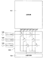
本発明の第1実施形態による2次元デジタルデータ取得素子の概略構成を図1に示す。本実施形態の2次元デジタルデータ取得素子100は、画素領域101と、負荷トランジスタ部102と、V選択回路(垂直選択回路)103と、H選択回路(水平選択回路)104と、読出し回路105と、1ビットA/D変換器(以下、1ビットADCとも云う)106と、タイミングジェネレータ(以下、TG回路とも云う)107とを備えている。読出し回路105は1行分のアナログ信号を保持する1Hメモリ回路を具備している。負荷トランジスタ部102と、V選択回路103と、H選択回路104と、読出し回路105と、1ビットADC106と、TG(タイミングジェネレータ)回路107とは、画素領域101の周囲に設けられる。なお、画素領域101と読出し回路105との間に画素固有の雑音を除去するためのCDS(相関二重サンプリング)回路を配置することも可能であるが、図1のようにCDS回路を配置しなくともかまわない。TG回路107は、別チップにしても構わないし、図1には記載されない信号処理回路に搭載してもよい。
FIG. 1 shows a schematic configuration of the two-dimensional digital data acquisition element according to the first embodiment of the present invention. The two-dimensional digital
画素領域101は、光電変換により入射光信号を電気信号に変換する光電変換素子を有する画素が二次元マトリクス状に配列されている。これらマトリクス状に配列された画素において発生した信号はV選択回路103およびH選択回路104によって以下のように時系列で出力される。
In the
V選択回路103により選択された行に配置された画素において光電変換された信号は、信号線207(図2参照)を介して読出し回路105によって読み出され保持される。読出し回路105内部の1Hメモリ回路に保持された信号は、H選択回路104により順次選択され、時系列で出力される。この時系列で出力される信号は1ビットADCを介して外部に1ビットデジタル信号として出力される。V選択回路103、H選択回路104、読出し回路105、および1ビットADC106のそれぞれの動作は、TG回路107から出力されるタイミングパルスによって制御される。
Signals photoelectrically converted in the pixels arranged in the row selected by the
図2は、本実施形態に係る画素領域101を構成する画素2と、負荷トランジスタ部102との回路図を示す。画素2は、いわゆるnチャネルMOSトランジスタからなる4トランジスタ構造であり、光電変換素子であるフォトダイオード201と、このフォトダイオード201に蓄積された信号電荷を検出ノード203に転送する転送トランジスタ202と、検出ノード203の電位をリセットするリセットトランジスタ204と、検出ノード203にゲートが接続された増幅トランジスタ205と、光電変換された信号を出力する画素を選択するための選択トランジスタ206とを有している。転送トランジスタ202、リセットトランジスタ204、および選択トランジスタ206のそれぞれのゲートに接続される転送トランジスタ制御線、リセットトランジスタ制御線、および選択トランジスタ制御線はV選択回路103によって所定のタイミングで制御される。
FIG. 2 is a circuit diagram of the
画素領域101の垂直方向に設けられる信号線207は、画素の選択トランジスタ206のソースに接続されている。負荷トランジスタ部102内の負荷トランジスタ208と、画素2の増幅トランジスタ205でソースフォロア回路を構成する。同一の信号線207に接続されている複数の画素のうち選択トランジスタ206がオン状態となった画素、すなわちV選択回路103によって選択された画素のみが上記のソースフォロア回路を構成し、選択された画素の検出ノード203の電位に応じた電位が、各列の信号線207に発生し、読出し回路105に読み出され保持される。
A
図3は、2次元デジタルデータ画像においてLow−Data単位データ領域に囲まれたHigh−Data単位データ領域1Hと、画素領域101の一部の相対的な位置関係を説明するための模式図であり、オーバーサンプリングとしてN=3の場合を示している。図3では、画素2として、5行×5列の25画素が配置された部分に、3行×3列の画素サイズのHigh−Data単位データ領域1Hが照射された様子を示しており、High−Data単位データ領域1Hの端部と画素2の境界とが一致していない。この状態で、超高速2次元デジタルデータ取得素子100の位置調整を行わない場合の一般的な状態を示している。
FIG. 3 is a schematic diagram for explaining the relative positional relationship between a part of the
図3の5行5列の25画素から得られる画素出力を図4に示す。 FIG. 4 shows a pixel output obtained from 25 pixels in 5 rows and 5 columns in FIG.
各画素2を(n行、m列)として表現すると、図3からもわかるように、(2,2)、(2,3)、(3,2)、(3,3)の4画素は画素全体がHigh−Data単位データ領域1Hに含まれており、その出力SはHigh−Data:SHに対応する。一方、上記4画素に接する12画素は、画素の一部がHigh−Data単位データ領域1Hに含まれており、その出力SはHigh−Dataより低い中間階調となっている。また、High−Data単位データ領域1Hに画素が含まれない9画素においては、その出力SはLow−Data:SLとなる。
When each
一方、2次元デジタルデータ画像においてHigh−Data単位データ領域に囲まれたLow−Data単位データ領域1Lと、画素領域101の一部の相対的な位置関係を説明するための模式図と、このときに得られる画素出力を、各々、図5、図6に示す。
On the other hand, in the two-dimensional digital data image, a schematic diagram for explaining the relative positional relationship between the Low-Data
画素2について、(n行、m列)として表現すると、図5からもわかるように、(2,2)、(2,3)、(3,2)、(3,3)の4画素は画素全体がLow−Data単位データ領域1Lに含まれており、その出力SはLow−Data:SLに対応する。一方、上記4画素に接する12画素は、画素の一部がLow−Data単位データ領域1Lに含まれており、その出力SはLow−Dataより高い中間階調となっている。また、Low−Data単位データ領域1Lに画素が含まれない9画素においては、その出力SはHigh−Data:SHとなる。
If the
通常のCMOSセンサであれば、図4または図6に示したアナログ出力をそのまま出力するか、あるいはNビットADCによりデジタル化しNビットデジタルデータとして出力する。 In the case of a normal CMOS sensor, the analog output shown in FIG. 4 or 6 is output as it is, or digitized by an N-bit ADC and output as N-bit digital data.
しかし、本実施形態では、図1の1ビットADC106により、図4、図6のアナログ出力を1ビットデジタル出力に変換し、出力する。1ビットADC106のしきい値電圧Vthは、SL<Vth<SHになるように設定され、SLとSHとを各々0、1に変換する。しかし、SL<SM<SHとなるような中間階調出力SMに対してはVthとSMとの関係により0、1いずれの出力が得られるかは確定しない。この不確定な出力を「?」として、図4、図6の各出力が1ビットADC106により変換された結果を図7,8に各々示す。図7、図8からわかるように、不確定な出力が1,0いずれであっても、1ビットデジタル出力が2個以上連続して同一の値であれば、その値により単位データ領域のHigh/Lowを認識することが可能である。
However, in the present embodiment, the 1-
図3〜図8では、同一の情報を示す単位データ領域が隣接する場合について説明していないが、その場合にはHigh−Data領域とLow−Data領域の境界部に発生する中間階調出力が無いので、同一のデジタルデータが2+3=5個以上連続して出力される。したがって、同一のデジタルデータが連続出力される画素数を外部回路に設けたカウンタによりカウントすることにより同一データが隣接した場合にもHigh/Lowを認識することが可能である。例えば、同一データが連続出力される画素数をnとすれば、n≦1はノイズであり無視し、2≦n≦4でSHあるいはSLに相当するデータ領域が1個、5≦n≦7でSHあるいはSLに相当するデータ領域が2個連続、(3m−1)≦n≦(3m+1)のときにSHあるいはSLに相当するデータ領域がm個連続、として認識することができる。
3 to 8 do not describe the case where the unit data areas indicating the same information are adjacent to each other, but in this case, an intermediate gradation output generated at the boundary between the High-Data area and the Low-Data area is output. Since there is no such data, the same digital data is continuously
外部回路では、1行分の1ビットメモリを利用して、上下に隣接する1ビットデジタルデータ間でデータが変化するかどうかを判定し、同様の方法で単位データ領域を認識することができる。なお、本実施形態においては、上記カウンタは外部回路に設けたが、後述する第2実施形態のように、2次元デジタルデータ取得素子100に内蔵させたカウンタ120であってもよい。
In the external circuit, it is possible to determine whether data changes between 1-bit digital data adjacent to each other by using 1-bit memory for one row, and to recognize a unit data area in the same manner. In the present embodiment, the counter is provided in an external circuit, but it may be a
1ビットADC106としては、図9(a)に示すように直列に接続された2段のインバータ回路すなわち、図9(b)に示すように直列に接続された2段のCMOSインバータ回路を用いることができる。図9(b)は一般的なCMOSインバータ回路を2段直列に接続したものであるが、出力の極性や動作マージンを考慮しなければ1段のインバータ回路でも構わないし、あるいは3段以上の直列接続構成にしてもよい。
As the 1-
図9(a)、9(b)の1ビットADCの電源電圧VDLは、他の電源電圧Vddと異なる電圧を与えるように独立制御可能とすることが可能であり、このようにすることがより好ましい。その理由は、電源電圧VDLを制御することにより1ビットADCのしきい値電圧Vthを制御可能であることにある。その詳細は他の実施形態で説明する。 The power supply voltage VDL of the 1-bit ADC in FIGS. 9A and 9B can be controlled independently so as to give a voltage different from the other power supply voltage Vdd. preferable. The reason is that the threshold voltage Vth of the 1-bit ADC can be controlled by controlling the power supply voltage VDL. Details thereof will be described in another embodiment.
また、超高速読出しのためには、読出し回路105を多線出力にすることが一般的に行われる。例えば10線出力とすることで、同一のクロック周波数のまま、出力のデータレートを10倍に増加することができる。読出し回路105が3線出力の場合の例を図10に示す。図の簡略化のために3線出力で信号線は6列としているが、実際には10線以上の出力と数百本あるいは千本以上の信号線により構成される。図10においては、H選択回路104からのH選択パルスは3列の選択トランジスタに同時に印加され、選択された3列の信号線に発生した画素出力情報を各々の選択トランジスタに接続された出力線に伝える。3本の出力線の各々には独立した1ビットADC106が接続され、1ビットデジタル出力に変換され、3本の出力端子から出力される。
In order to perform ultra-high-speed reading, it is generally performed that the
このとき、3個の1ビットADC106の特性、すなわち、1ビットAD変換におけるしきい値電圧Vthが揃っていることが重要である。1ビットADC106として、図9に示したCMOSインバータ回路を用いた場合、PMOSトランジスタとNMOSトランジスタのそれぞれのしきい値電圧Vthp、Vthnが一定であることが重要である。同一基板内でのトランジスタのしきい値電圧Vthのばらつきの主原因はチャネル領域の不純物数の統計的な揺らぎであることが知られている。そして、1ビットADC106のトランジスタは、画素内部の微細トランジスタと異なり、周辺回路のトランジスタであるので、チャネル面積を十分に確保することでVthp,Vthnを一定に保つことが可能である。また、基板が異なる場合には、電子・正孔の移動度、ゲート酸化膜厚によりCMOSインバータのしきい値電圧Vthは変化するが、本実施形態においては同一基板上のトランジスタ特性が揃っていれば良いので、基板が異なる場合は関係ない。
At this time, it is important that the characteristics of the three 1-
このような多線読出し構造の場合、画素出力をMビットADCによりMビットのデジタルデータに変換・出力しようとすると、極めて多数の出力ピンが必要となる。たとえば、10線読出し、10ビット出力というCMOSセンサが製品化されているが、この場合、出力ピンだけで10×10=100本にもなり、パッケージコストを下げることが困難である。 In the case of such a multi-line readout structure, an extremely large number of output pins are required to convert and output the pixel output to M-bit digital data by the M-bit ADC. For example, a CMOS sensor with 10-line readout and 10-bit output has been commercialized. In this case, the number of output pins alone is 10 × 10 = 100, and it is difficult to reduce the package cost.
それに対して、本実施形態では、高速読出しのために10線読出し構造としても、出力データは1ビットデジタル信号であるので出力ピンはわずか10本にとどまる。この出力ピン数は、1線読出・10ビット出力の標準CMOSセンサと同一であり、低価格のパッケージを使用することが可能であり、また、外部回路とのI/F(インターフェース)も簡略化でき、システム全体を小型化・低コスト化することが可能となる。 On the other hand, in this embodiment, even if a 10-line readout structure is used for high-speed readout, the output data is a 1-bit digital signal, so there are only 10 output pins. The number of output pins is the same as that of a standard CMOS sensor with 1-line readout and 10-bit output, and it is possible to use a low-priced package. Also, I / F (interface) with external circuits is simplified. Thus, the entire system can be reduced in size and cost.
以上説明したように、本実施形態によれば、標準的な画素構成を持つCMOSセンサ素子をベースにした、簡単なデバイス構成により超高速な2次元デジタルデータ取得素子を得ることができ、小型化、低コスト化が可能である。 As described above, according to the present embodiment, an ultrafast two-dimensional digital data acquisition element can be obtained with a simple device configuration based on a CMOS sensor element having a standard pixel configuration, and can be downsized. Cost reduction is possible.
さらに、高速動作のために多線読出しを行う場合、読み出し線数をKとした場合、従来のMビット出力素子ではM×K本の出力ピンが必要なのに対して、K本の出力ピンで十分でありチップコストのみならずパッケージコストも大幅にコストダウンすることが可能である。その上、出力が1ビットデジタル出力であるので、外部回路による2次元デジタルデータ再構築プロセスは大幅に単純化され、超高速な2次元デジタルデータ取得装置としての大幅な小型化、低コスト化が可能となる。 Furthermore, when performing multi-line readout for high-speed operation, if the number of readout lines is K, the conventional M-bit output element requires M × K output pins, whereas K output pins are sufficient. Therefore, not only the chip cost but also the package cost can be significantly reduced. In addition, since the output is a 1-bit digital output, the process of reconstructing the two-dimensional digital data by an external circuit is greatly simplified, and the size and cost of the ultra-fast two-dimensional digital data acquisition device can be greatly reduced. It becomes possible.
(第2実施形態)
本発明の第2実施形態による2次元デジタルデータ取得素子の概略構成を図11に示す。本実施形態の2次元デジタルデータ取得素子100Aは、図1に示す第1実施形態の2次元デジタルデータ取得素子100において、1ビットADC106と出力端子との間に、論理演算処理回路108と、カウンタ120とを設けた構成となっている。
(Second Embodiment)
FIG. 11 shows a schematic configuration of a two-dimensional digital data acquisition element according to the second embodiment of the present invention. The two-dimensional digital
第1実施形態において説明したように、1ビットデジタル出力を外部回路により処理することで、2次元デジタルデータを再構築可能である。本実施形態においては、外部回路における処理をより簡略化するために、上記1ビットデジタル出力を、オンチップ化した論理演算処理回路108により演算処理し、その演算結果を1ビットデジタルデータとして出力し、この出力をカウンタ120によりカウントし、このカウント値により単位データを認識する。
As described in the first embodiment, two-dimensional digital data can be reconstructed by processing the 1-bit digital output by an external circuit. In this embodiment, in order to further simplify the processing in the external circuit, the 1-bit digital output is arithmetically processed by the on-chip logic
論理演算処理回路108の一具体例を図12に示す。1ビットADC106の出力を分岐し、一方をAND回路108bに直接入力し、もう一方を遅延回路108aを介してAND回路108bに入力する。そしてAND回路108bによる演算結果を出力する。遅延回路108aでは、1画素分の遅延を行う。図12に示す画素データ間演算処理回路108によって、連続的に読み出される隣接画素データ間のAND演算が行われ、2画素連続でHigh−Dataデジタル出力:SHが入力された場合にのみSHを出力する。
A specific example of the logical
図3、図5に示す2次元デジタルデータが入射し、図4、図6に示す画素出力が得られ、1ビットADC106の出力として図7、図8に示す1ビットデジタルデータが論理演算処理回路108に入力した場合の演算処理結果を図13、図14に示す。中間階調出力が存在するために不確定な1ビットデジタルデータ「?」が存在するが、High−Data領域が存在する場合にはSHが最低でも1画素分出力され、逆にLow−Data領域が存在する場合にはSLが最低でも3画素連続で出力される。このため、例えば、High−Dataに注目すれば、SHが出現した場合をHigh−Dataとして認識することができる。また、二つのHigh−Data領域が隣接した場合には、SHが最低でも4画素連続して出力されるので、第1実施形態と同様に、SHが出力された場合にはSHが連続で出力される画素数をカウンタ120によりカウントすればよい。このカウント数によりHigh−Data領域の連続数が判定できる。SHが連続出力される画素数をnとすれば、1≦n≦3でHigh−Data領域が1個、4≦n≦6でHigh−Data領域が2個連続、(3m−2)≦n≦3mのときにHigh−Data領域がm個連続、として認識することができる。なお、外部回路においても、1行分の1ビットメモリを利用して、上下に隣接する1ビットデジタルデータ間でAND演算を行い、同様の方法でHigh−Data領域を認識することができる。
The two-dimensional digital data shown in FIGS. 3 and 5 are incident, and the pixel outputs shown in FIGS. 4 and 6 are obtained. As the output of the 1-
本実施形態のように、オンチップで画素データ間の論理演算処理を行うことは外部回路における処理プロセスへの負荷を軽減するという他にも重要な効果がある。それは、白傷画像欠陥による誤出力をオンチップで防止することができるという効果である。 Performing logical operation processing between pixel data on-chip as in the present embodiment has an important effect other than reducing the load on the processing process in the external circuit. This is an effect that an erroneous output due to a white scratch image defect can be prevented on-chip.
白傷画像欠陥とは、画素内部のフォトダイオードや検出ノードの部分に結晶欠陥や重金属汚染等に起因する発生中心が形成されてしまい、画素出力が入射光量によらず、常にHigh−Dataを出力してしまうものである。一般に、良くコントロールされた基板や製造プロセスにより、白傷画像欠陥の発生率は低減されており、白傷画像欠陥が隣接画素に連続的に発生することは極めて稀である。したがって、白傷画像欠陥は1画素単独の点欠陥である。白傷画像欠陥が問題となるのは、Low−Data領域においてであり、本来SLが出力される画素においてSHが出力されてしまう。しかし、本実施形態のように画素データ間に演算処理回路108による論理演算を行えば、白傷画像欠陥による画素出力はオンチップで除去される。
The white defect image defect means that the generation center due to crystal defects or heavy metal contamination is formed in the photodiode or detection node part inside the pixel, and the pixel output always outputs High-Data regardless of the incident light quantity. It will end up. In general, the rate of occurrence of white defect image defects is reduced by a well-controlled substrate or manufacturing process, and it is extremely rare that white defect image defects occur continuously in adjacent pixels. Therefore, the white defect image defect is a point defect of one pixel alone. The white flaw image defect becomes a problem in the Low-Data region, and SH is output in a pixel that originally outputs SL. However, if a logical operation is performed between the pixel data by the
逆に、入射光量によらず常にLow−Dataを出力するという黒傷画像欠陥がHigh−Data領域に存在した場合、本実施形態の画素データ間演算処理回路108においてHigh−Data領域が失われることが懸念されるが、出力が常にLow−Dataとなるような黒傷画像欠陥は、良くコントロールされた製造プロセスにより、ほぼ完全に排除されている。
On the other hand, when a black flaw image defect that always outputs Low-Data regardless of the amount of incident light exists in the High-Data area, the High-Data area is lost in the inter-pixel
また、第1実施形態において説明したように、超高速読出しのためには、読出し回路105を多線出力にすることが一般的に行われる。例えば10線出力とすることで、同一のクロック周波数のまま、出力のデータレートを10倍に増加することができる。読出し回路105が3線出力の場合の構成例を図15に示す。図の簡略化のために3線出力で信号線は6列としているが、実際には10線以上の出力と数百本あるいは千本以上の信号線により構成される。図15においては、H選択回路104からのH選択パルスは3列の選択トランジスタに同時に印加され、選択された3列の信号線に発生した画素出力情報を各々の選択トランジスタに接続された出力線に伝える。3本の出力線の各々には独立した1ビットADC106が接続され、1ビットデジタル出力に変換され、その1ビットデジタル出力に対して演算処理を行い、演算結果を3本の出力端子から出力する。
In addition, as described in the first embodiment, the
第1実施形態において説明したように、3個の1ビットADC106の特性、すなわち、1ビットAD変換におけるVthを揃えることは可能であり、問題ない。図15では、多線読出しにおける画素データ間演算処理回路108が図12に示した画素データ間演算処理回路108と異なっている。
As described in the first embodiment, it is possible to align the characteristics of the three 1-
多線読出しにおいては、隣接列が同時に選択・出力されるので、各読出し線から1ビットADCを介して出力されたデジタルデータをAND回路108bに直接に入力することが可能である。そして、隣接列が異なるタイミングで選択・出力される列に関してのみ、遅延回路108aを介してAND回路108bに入力している。したがって、遅延回路108bは読出し線の本数によらず1個のみでよい。
In multi-line reading, since adjacent columns are simultaneously selected and output, digital data output from each read line via a 1-bit ADC can be directly input to the AND
このような多線読出し構造の場合、従来のように、画素出力をMビットADCによりMビットのデジタルデータに変換・出力しようとすると、極めて多数の出力ピンが必要となる。例えば、10線読出し、10ビット出力というCMOSセンサが製品化されているが、この場合、出力ピンだけで10×10=100本にもなり、パッケージコストを下げることが困難である。 In the case of such a multi-line readout structure, if an attempt is made to convert and output the pixel output to M-bit digital data by the M-bit ADC as in the prior art, an extremely large number of output pins are required. For example, CMOS sensors for 10-line readout and 10-bit output have been commercialized. In this case, the number of output pins alone is 10 × 10 = 100, and it is difficult to reduce the package cost.
それに対して、本実施形態では、高速読出しのために10線読出し構造としても、出力データは1ビットデジタル信号であるので出力ピンはわずか10本にとどまる。この出力ピン数は、1線読出・10ビット出力の標準CMOSセンサと同一であり、低価格のパッケージを使用することが可能であり、また、外部回路とのI/Fも簡略化でき、システム全体を小型化・低コスト化することが可能となる。 On the other hand, in this embodiment, even if a 10-line readout structure is used for high-speed readout, the output data is a 1-bit digital signal, so there are only 10 output pins. The number of output pins is the same as that of a standard CMOS sensor with one-line readout and 10-bit output, and a low-cost package can be used. Also, the I / F with external circuits can be simplified, and the system The whole can be reduced in size and cost.
以上説明したように、本実施形態によれば、標準的な画素構成を持つCMOSセンサ素子をベースにした、簡単なデバイス構成により超高速な2次元デジタルデータ取得素子を得ることができ、小型化、低コスト化が可能であり、また白傷画像欠陥の影響をオンチップで排除することで素子の製造歩留りを向上し、さらに低コスト化できる。 As described above, according to the present embodiment, an ultrafast two-dimensional digital data acquisition element can be obtained with a simple device configuration based on a CMOS sensor element having a standard pixel configuration, and can be downsized. The cost can be reduced, and the production yield of the device can be improved and the cost can be further reduced by eliminating the influence of the white defect image defect on-chip.
さらに、高速動作のために多線読出しを行う場合、読み出し線数をKとした場合、従来のMビット出力素子ではM×K本の出力ピンが必要なのに対して、K本の出力ピンで十分でありチップコストのみならずパッケージコストも大幅にコストダウンすることが可能である。 Furthermore, when performing multi-line readout for high-speed operation, if the number of readout lines is K, the conventional M-bit output element requires M × K output pins, whereas K output pins are sufficient. Therefore, not only the chip cost but also the package cost can be significantly reduced.
その上、出力が画素データ間で演算された1ビットデジタル出力であるので、外部回路による2次元デジタルデータ再構築プロセスは大幅に単純化され、超高速な2次元デジタルデータ取得装置としての大幅な小型化、低コスト化が可能となる。 In addition, since the output is a 1-bit digital output calculated between pixel data, the process of reconstructing the two-dimensional digital data by an external circuit is greatly simplified, and the output as a very high-speed two-dimensional digital data acquisition device is greatly simplified. Miniaturization and cost reduction are possible.
なお、本実施形態においては、カウンタ120を2次元デジタルデータ取得素子100Aに内蔵させたが、外部に設けてもよい。
In the present embodiment, the
(第3実施形態)
本発明の第3実施形態による2次元デジタルデータ取得素子の概略構成を図16に示す。本実施形態の2次元デジタルデータ取得素子100Bは、図1に示す第1実施形態の2次元デジタルデータ取得素子100において、アナログバッファ回路109を新たに設け、読出し回路105の出力が1ビットADC106に入力されるだけでなく、アナログバッファ回路109にも入力されるようにした構成となっている。
(Third embodiment)
FIG. 16 shows a schematic configuration of a two-dimensional digital data acquisition element according to the third embodiment of the present invention. In the two-dimensional digital
本実施形態の2次元デジタルデータ取得素子100Bによれば、1ビットデジタル出力だけでなく、画素からのアナログ出力を得ることが可能であり、このアナログ出力を用いて1ビットADC106の動作を最適化することが可能でかつ超高速な2次元デジタルデータ取得素子を得ることができる。なお、アナログバッファ回路109としては、入力インピーダンスが高いバッファ回路として、例えば図17に示すソースフォロア回路を用いることが可能である。
According to the two-dimensional digital
本実施形態の2次元デジタルデータ取得素子100Bにおける、1ビットADC106の動作の最適化について、以下に説明する。
The optimization of the operation of the 1-
2次元デジタルデータのHigh−Data領域の抽出については、第1実施形態および第2実施形態において説明したが、High−Data領域において発生する画素出力は、2次元デジタルデータを形成するための光源の光強度により変化する。例えば、ホログラフィックストレージ装置においては、2次元デジタルデータであるホログラフィック像を得るために400nm程度の短波長レーザー光源からの参照光を媒体である光ディスクに照射するが、このレーザー光源の光強度が経時変化することで、2次元デジタルデータのHigh−Data領域の照度が変化し、その結果、High−Data領域において発生する画素出力が変化することが考えられる。あるいは、媒体である光ディスクの状態により光経路における光学的損失が変化することでも、同様に2次元デジタルデータのHigh−Data領域の照度が変化し、その結果、High−Data領域において発生する画素出力が変化することが考えられる。これらの場合には、1ビットADC106のしきい値電圧Vthを調整することで、1ビットADC106の動作を最適化することが可能である。
The extraction of the high-data area of the two-dimensional digital data has been described in the first embodiment and the second embodiment, but the pixel output generated in the high-data area is the light source for forming the two-dimensional digital data. Varies with light intensity. For example, in a holographic storage device, in order to obtain a holographic image that is two-dimensional digital data, reference light from a short-wavelength laser light source of about 400 nm is irradiated to an optical disk as a medium. By changing with time, the illuminance of the High-Data area of the two-dimensional digital data changes, and as a result, the pixel output generated in the High-Data area may change. Alternatively, even if the optical loss in the optical path changes depending on the state of the optical disk as the medium, the illuminance of the High-Data area of the two-dimensional digital data also changes, and as a result, the pixel output generated in the High-Data area May change. In these cases, the operation of the 1-
本実施形態の2次元デジタルデータ取得素子100Bでは、アナログバッファ回路109を介してアナログ出力を得ることができるので、このアナログ出力を利用することで、1ビットADC106のしきい値電圧Vthを調整し、その動作を最適化することができる。
In the two-dimensional digital
2次元デジタルデータを取得する際には、媒体である光ディスクを装置にセットする。その光ディスクをセットするたびに、少なくとも1フレーム分のHigh−Dataアナログ出力を外部回路に読出し、その1フレーム分のHigh−Dataアナログ出力データから、High−Data領域において発生する画素出力を知り、その値を元に1ビットADC106のしきい値電圧Vthを調整することで、1ビットADC106の動作を最適化することが可能である。例えば、最も単純な方法としては、1フレーム分のアナログ出力データから最大となるアナログ出力:Vmaxを抽出し、1ビットADC106のしきい値電圧VthがVmax/2になるように設定する方法がある。特に、1ビットADC106として、図9に示すように、CMOSインバータ回路を用いた場合には、このVmaxと同じ電圧をVDLに与えることで、1ビットADC106のしきい値電圧VthをVmax/2に設定することが可能である。それは、CMOSインバータ回路のしきい値電圧Vthは、CMOSインバータ回路を構成するnMOS、pMOSの各トランジスタについて、以下の条件があれば、Vth=VDL/2となるからである。
βn=βp
Vthn=−Vthp
ただし、
βn=μn・Cox・(Weffn/Leffn)
βp=μp・Cox・(Weffp/Leffp)
ここで、μnは電子の移動度、μpは正孔の移動度、Coxは単位面積あたりのゲート酸化膜容量、Weffnは、nMOSトランジスタの有効チャネル幅、WeffpはpMOSトランジスタの有効チャネル幅、LeffnはnMOSトランジスタの有効チャネル長、LeffpはpMOSトランジスタの有効チャネル長である。
When acquiring two-dimensional digital data, an optical disk as a medium is set in the apparatus. Each time the optical disk is set, at least one frame of High-Data analog output is read out to an external circuit, and the one-frame High-Data analog output data is used to know the pixel output generated in the High-Data area. The operation of the 1-
βn = βp
Vthn = −Vthp
However,
βn = μn · Cox · (Weffn / Leffn)
βp = μp · Cox · (Weffp / Leffp)
Here, μn is the mobility of electrons, μp is the mobility of holes, Cox is the gate oxide film capacity per unit area, Weffn is the effective channel width of the nMOS transistor, Weffp is the effective channel width of the pMOS transistor, and Leffn is The effective channel length of the nMOS transistor, Leffp, is the effective channel length of the pMOS transistor.
この条件は、チャネル不純物濃度、チャネルサイズ等の設計により実現可能である。 This condition can be realized by designing the channel impurity concentration, the channel size, and the like.
また、この条件が満たされなくとも、CMOSインバータのしきい値電圧VthをVDLで表現することは可能であるので、その場合には、Vth=Vmax/2となるようにVDLを設定すればよい。 Even if this condition is not satisfied, the threshold voltage Vth of the CMOS inverter can be expressed by VDL. In this case, VDL may be set so that Vth = Vmax / 2. .
以上説明したように、アナログ出力情報を元に、1ビットADCの動作を最適化することができる。 As described above, the operation of the 1-bit ADC can be optimized based on the analog output information.
なお、1フレーム分のHigh−Dataアナログ出力データから、High−Data領域において発生する画素出力を知り、その値を元に1ビットADCのVthを画素ごとに調整することで、1ビットADCの動作を画素ごとに最適化することも可能である。この場合、図18に示すように、外部フレームメモリ301に1フレーム分のHigh−Dataアナログ出力データを保持し、該当画素のADC動作と同期するように、外部フレームメモリ301に保持されたHigh−Dataアナログ出力データをADCのVDLとして供給すればよい。
The operation of the 1-bit ADC is obtained by knowing the pixel output generated in the High-Data area from the High-Data analog output data for one frame and adjusting the Vth of the 1-bit ADC for each pixel based on the value. It is also possible to optimize for each pixel. In this case, as shown in FIG. 18, High-Data analog output data for one frame is held in the
前述したように、Vth=VDL/2が満たされない場合においては、High−Dataアナログ出力データVHDiに対して適当な変換処理を行うことで、Vthi=VHDi/2となるようなVDLiを与えることが可能である。ここで、添え字のiは、画素ごとのデータという意味である。 As described above, when Vth = VDL / 2 is not satisfied, VDL i such that Vth i = VHD i / 2 is obtained by performing appropriate conversion processing on the High-Data analog output data VHD i . It is possible to give Here, the subscript i means data for each pixel.
1ビットADC106のしきい値電圧Vthを画素ごとに調整する場合の装置構成と、その動作フローを図19に示す。まず、媒体をセットする(図19のステップS1)。その後、本実施形態のデータ取得素子100Bを用いて1フレームHigh−Dataを取得する(図19のステップS2)。続いて、アナログバッファ回路109の出力を1フレーム分、フレームメモリ301に記憶させる(図19のステップS3)。そして、フレームメモリ301からの画素ごとのHigh−Data出力に応じた電圧を1ビットADC106に与えながらデータ取得動作を行う(図19のステップS4)。このとき、必要に応じて外部の変換回路302で電圧変換を行う(図19のステップS5)。
FIG. 19 shows a device configuration and its operation flow when the threshold voltage Vth of the 1-
また、前述の最も単純な方法である、1フレーム分のアナログ出力データから最大となるアナログ出力Vmaxを抽出し、1ビットADC106のしきい値電圧VthがVmax/2になるように設定する方法においても、その動作フロー等は図19と同じであり、その場合、図18に示す変換回路302においてVmaxの抽出を行うことが可能である。また、Vmaxを変換回路302の内部に保持・記憶することで、それ以降のフレームメモリ動作を終了させることもできる。
In the simplest method described above, the maximum analog output Vmax is extracted from the analog output data for one frame, and the threshold voltage Vth of the 1-
このアナログ出力は、1ビットADCの動作を最適化するためにのみ使用するので、図17に示すソースフォロア回路の電源電圧VDをパルス駆動する、あるいは負荷トランジスタのゲート電圧VGLをパルス駆動することで、デジタル出力時にアナログバッファ回路109の動作を停止することも可能であり、消費電力を抑制するためには好ましいといえる。
This analog output is 1 because only used to optimize the operation of the bit ADC, pulsing power supply voltage V D of the source follower circuit shown in FIG. 17, or pulsing drive the gate voltage VGL of the load transistor Thus, it is possible to stop the operation of the
また、第1実施形態および第2実施形態において説明したように、超高速読出しのためには、読出し回路105を多線出力にすることが一般的に行われる。例えば、10線出力とすることで、同一のクロック周波数のまま、出力のデータレートを10倍に増加することができる。その場合には、多線読出しのための読出し線と同数のアナログバッファ回路を配置することで対応でき、その場合にはデジタル出力のピン数と同数のアナログ出力ピンが必要となる。
Further, as described in the first embodiment and the second embodiment, the
あるいは、アナログ出力と1ビットデジタル出力を同時に得る必要が無ければ、出力ピンをアナログ・デジタルで共用し、スイッチで切り替えて使用することも可能であり、その場合には出力ピンが増加することもなく、より好ましいといえる。 Alternatively, if it is not necessary to obtain an analog output and a 1-bit digital output at the same time, the output pin can be shared between analog and digital and used by switching with a switch. In that case, the output pin may increase. It is not preferable.
さらに、本実施形態を図11に示した第2実施形態と組み合わせて実施することも可能である。 Furthermore, this embodiment can be implemented in combination with the second embodiment shown in FIG.
以上説明したように、本実施形態によれば、アナログ出力データを演算して得た結果から、1ビットADCのしきい値電圧Vthを調整し、その動作を最適化することができ、光源の変動・媒体の状態の変化等による2次元デジタルデータの照度変化が発生しても、安定なデータ読み取りが可能でかつ超高速な2次元デジタルデータ取得素子および2次元デジタルデータ取得装置を得ることができる。 As described above, according to the present embodiment, the threshold voltage Vth of the 1-bit ADC can be adjusted from the result obtained by calculating the analog output data, and the operation can be optimized. It is possible to obtain a two-dimensional digital data acquisition device and a two-dimensional digital data acquisition device capable of stable data reading and an ultra-high speed even when the illuminance change of the two-dimensional digital data occurs due to fluctuations or changes in the state of the medium. it can.
また、第1実施形態、または第2実施形態と同様の効果も得ることができる。 Moreover, the same effect as 1st Embodiment or 2nd Embodiment can also be acquired.
(第4実施形態)
本発明の第4実施形態による2次元デジタルデータ取得素子の概略構成を図20に示す。本実施形態の2次元デジタルデータ取得素子100Cは、図1に示す第1実施形態の2次元デジタルデータ取得素子100において、1Hメモリ回路110および論理演算回路111を新たに設けた構成となっている。
(Fourth embodiment)
FIG. 20 shows a schematic configuration of a two-dimensional digital data acquisition element according to the fourth embodiment of the present invention. The two-dimensional digital
この1Hメモリ回路110は、2個の第1および第2の1Hメモリ(図示せず)と、これら第1および第2の1Hメモリ間でデータをコピーするコピー部(図示せず)とを備えている。そして、これら第1および第2の1HメモリはH選択回路104により同一列が選択される。
The
次に、この1Hメモリ回路110および論理演算回路111の動作を説明する。
ステップ1:先頭行データである1ビットADC106の出力を第1の1Hメモリに記憶する。
ステップ2:第1の1Hメモリに記憶されたデータをコピー部によって第2の1Hメモリにコピーし、記憶させる。
ステップ3:次行データである1ビットADC106の出力を第1の1Hメモリに記憶する。
ステップ4:ステップ3の記憶動作と並行して1ビットADC106の出力と同期して第2の1Hメモリから出力される前行の出力と、1ビットADC106との出力とを、論理演算回路111において順次、論理演算を行いながら、「列内」の演算結果を時系列で出力する。
ステップ5:第1の1Hメモリから第2の1Hメモリにデータをコピーする。
ステップ6:ステップ3乃至ステップ5をデータが無くなるまで繰り返す。
Next, operations of the
Step 1: The output of the 1-
Step 2: The data stored in the first 1H memory is copied and stored in the second 1H memory by the copy unit.
Step 3: The output of the 1-
Step 4: In parallel with the storage operation of
Step 5: Copy data from the first 1H memory to the second 1H memory.
Step 6: Repeat steps 3 to 5 until there is no more data.
このように構成された本実施形態の2次元デジタルデータ取得素子は、水平方向に隣接する画素間の論理演算処理に加えて、垂直方向に隣接する画素間の論理演算処理機能をオンチップで実現しており、第1実施形態に比べて、外部回路における演算処理を大幅に軽減可能であり、第1実施形態以上に、外部回路の大幅な小型化および大幅な低コスト化が可能となる。 The two-dimensional digital data acquisition element of this embodiment configured in this way realizes on-chip a logical operation processing function between pixels adjacent in the vertical direction in addition to a logical operation processing between pixels adjacent in the horizontal direction. Compared to the first embodiment, the arithmetic processing in the external circuit can be greatly reduced, and the external circuit can be greatly reduced in size and cost significantly compared to the first embodiment.
なお、本実施形態においては、1ビットADC106が1個しか設けられていなかったが、例えば、図10に示すように多線読出し構造として、1ビットADC106が複数個設けられていてもよい。この場合、1Hメモリ回路110および論理演算回路111も1ビットADC106の個数に応じて設ける必要がある。
In the present embodiment, only one 1-
(第5実施形態)
本発明の第5実施形態による2次元デジタルデータ取得素子の概略構成を図21に示す。本実施形態の2次元デジタルデータ取得素子100Dは、図11に示す第2実施形態の2次元デジタルデータ取得素子100Aにおいて、1Hメモリ回路110および論理演算回路111を新たに設けた構成となっている。
(Fifth embodiment)
FIG. 21 shows a schematic configuration of a two-dimensional digital data acquisition element according to the fifth embodiment of the present invention. The two-dimensional digital
この1Hメモリ回路110は、2個の第1および第2の1Hメモリ(図示せず)と、これら第1および第2の1Hメモリ間でデータをコピーするコピー部(図示せず)とを備えている。そして、これら第1および第2の1HメモリはH選択回路104により同一列が選択される。
The
次に、この1Hメモリ回路110および論理演算回路111の動作を説明する。
ステップ1:先頭行データである画素データ間演算処理回路108の出力を第1の1Hメモリに記憶する。
ステップ2:第1の1Hメモリに記憶されたデータをコピー部によって第2の1Hメモリにコピーし、記憶させる。
ステップ3:次行データである画素データ間演算処理回路108の出力を第1の1Hメモリに記憶する。
ステップ4:ステップ3の記憶動作と並行して画素データ間演算処理回路108の出力と同期して第2の1Hメモリから出力される前行の出力と、画素データ間演算処理回路108の出力とを、論理演算回路111において順次、論理演算を行いながら、「列内」の演算結果を時系列で出力する。
ステップ5:第1の1Hメモリから第2の1Hメモリにデータをコピーする。
ステップ6:ステップ3乃至ステップ5をデータが無くなるまで繰り返す。
Next, operations of the
Step 1: The output of the inter-pixel data
Step 2: The data stored in the first 1H memory is copied and stored in the second 1H memory by the copy unit.
Step 3: The output of the inter-pixel data
Step 4: In parallel with the storage operation of
Step 5: Copy data from the first 1H memory to the second 1H memory.
Step 6: Repeat steps 3 to 5 until there is no more data.
このように構成された本実施形態の2次元デジタルデータ取得素子は、水平方向に隣接する画素間の論理演算処理に加えて、垂直方向に隣接する画素間の論理演算処理機能をオンチップで実現しており、外部回路における演算処理を大幅に軽減可能であり、第2実施形態以上に、外部回路の大幅な小型化および大幅な低コスト化が可能となる。 The two-dimensional digital data acquisition element of this embodiment configured in this way realizes on-chip a logical operation processing function between pixels adjacent in the vertical direction in addition to a logical operation processing between pixels adjacent in the horizontal direction. Therefore, the arithmetic processing in the external circuit can be greatly reduced, and the external circuit can be significantly reduced in size and cost significantly compared to the second embodiment or more.
なお、本実施形態においては、1ビットADC106が1個しか設けられていなかったが、例えば、図10に示すように複数個設けられていてもよい。この場合、画素データ間演算処理回路108、1Hメモリ回路110、および論理演算回路111も1ビットADC106の個数に応じて設ける必要がある。
In the present embodiment, only one 1-
(第6実施形態)
次に、本発明の第6実施形態による2次元デジタルデータ取得素子の駆動方法を説明する。本実施形態の駆動方法は、上記第1乃至第5実施形態のいずれかによる2次元デジタルデータ取得素子の駆動に用いられ、その駆動タイミングチャートを図22に示す。
(Sixth embodiment)
Next, a method for driving a two-dimensional digital data acquisition element according to a sixth embodiment of the present invention will be described. The driving method of this embodiment is used for driving the two-dimensional digital data acquisition element according to any one of the first to fifth embodiments, and a driving timing chart thereof is shown in FIG.
図22に示したタイミングチャートの特徴は、転送トランジスタ202を全画素で同時に制御していることにあり、その目的とするところは、全画素で同時に2次元デジタルデータを取得することにある。
A feature of the timing chart shown in FIG. 22 is that the
一般的に、CMOSセンサの読出し動作は行単位で実行され、その際にはCDS回路による画素固有雑音除去を目的に、検出ノードをリセットした状態での暗時信号読出しと、信号電荷をフォトダイオードから検出ノードに転送した状態での明時信号読出しを行う。その結果、フォトダイオードにおいて信号電荷が蓄積する時間帯、言い換えれば、時刻は、行ごとに異なってしまう。 In general, the readout operation of the CMOS sensor is performed in units of rows. At that time, for the purpose of removing pixel-specific noise by the CDS circuit, readout of the dark signal with the detection node reset and the signal charge to the photodiode are performed. The signal at the time of light is read out in a state where it is transferred to the detection node. As a result, the time zone in which the signal charge is accumulated in the photodiode, in other words, the time differs for each row.
また、ホログラフィックストレージ装置等の超高速2次元デジタルデータ取得装置では、2次元デジタルデータを全画素で同時に読み取り、その後のデータ読出し期間を利用して、光ディスク等の媒体を移動し、次の2次元デジタルデータを形成することにより、効率的に高速読出しを実現することが可能である。 Also, in an ultra-high-speed two-dimensional digital data acquisition device such as a holographic storage device, two-dimensional digital data is simultaneously read by all pixels, and a medium such as an optical disk is moved using the subsequent data reading period. By forming the dimensional digital data, it is possible to realize high-speed reading efficiently.
また、図22に示すように、転送トランジスタ202を全画素同時にオン動作させ、フォトダイオード201に蓄積した信号電荷を全画素同時に検出ノード203に転送しており、上記の効率的な高速読出し動作に対応している。図22を参照して、素子動作を説明する。
In addition, as shown in FIG. 22, the
まず、媒体が固定された状態で、転送トランジスタ202とリセットトランジスタ204を全画素同時にオンし、全画素のフォトダイオード201、検出ノード203をリセットする(時刻T1)。
First, in a state where the medium is fixed, the
次に、一定時間経過後、全画素の転送トランジスタ202を同時にオンし、全画素同時に、フォトダイオード201に蓄積した信号電荷を検出ノード203に転送する(時刻T2)。期間(T2−T1)が、いわゆる蓄積期間となり、この期間は光ディスク等の媒体を固定し、2次元デジタルデータが変化しないようにする。
Next, after a predetermined time has elapsed, the
信号電荷の転送が完了した後、光ディスク等の媒体を移動し、次の2次元デジタルデータを発生させる準備を行う。 After the transfer of signal charges is completed, a medium such as an optical disk is moved to prepare for generating the next two-dimensional digital data.
検出ノード203に転送された信号電荷は、行選択パルスV1、V2、・・・、Vnにより信号線207の電圧に変換される。行選択パルスV1により発生した信号線電圧は、H選択パルスがH選択回路104から出力されることにより読出し回路105に読み出される。
The signal charges transferred to the
H選択パルスの終了に続き、次の行選択パルスV2で新たな信号線電圧が発生し、H選択パルスがH選択回路104から出力されることにより読出し回路に読み出され、以降、最後の行の信号読出しが完了するまで繰り返される。
Following the end of the H selection pulse, a new signal line voltage is generated at the next row selection pulse V2, and the H selection pulse is output from the
全ての信号読出しが完了した後、全画素同時に転送トランジスタ202とリセットトランジスタ204をオンにし、全画素のフォトダイオード201、検出ノード203をリセットする。
After all the signals are read out, the
このリセット動作が行われるまでに、光ディスク等の媒体の移動は完了し、次の2次元デジタルデータが発生している。 By the time this reset operation is performed, the movement of the medium such as the optical disk is completed, and the next two-dimensional digital data is generated.
本実施形態の駆動方法によれば、全画素同時の積分動作を行うことにより、2次元デジタルデータを形成する光ディスク等の媒体を固定する期間を短縮することが可能であり、また、検出ノードに転送した信号電荷を順次読み出す動作を行っている期間に、光ディスク等の媒体を移動し、次の2次元デジタルデータを形成する準備を行うことができるので、効率的に超高速2次元デジタルデータ読出しを行うことが可能となる。 According to the driving method of the present embodiment, it is possible to shorten the period for fixing a medium such as an optical disk that forms two-dimensional digital data by performing an integration operation at the same time for all pixels. During the period in which the transferred signal charges are sequentially read out, it is possible to move the medium such as the optical disk and prepare for the next two-dimensional digital data, so that the ultra-high-speed two-dimensional digital data can be read efficiently. Can be performed.
さらに、必要に応じて、画素領域101と読出し回路105との間にCDS回路を設けて、各行の検出ノード情報を信号線に読出した後に、該当行の検出ノードをリセットし、検出ノード情報を含む信号線出力と、検出ノードをリセットした状態での信号線出力との差分を取ることも可能である。この場合、検出ノードのリセットに起因するkTC雑音の除去はできないが、画素内の増幅トランジスタの閾値ばらつきに起因する画素固有の雑音を除去することが可能である。
Further, if necessary, a CDS circuit is provided between the
(第7実施形態)
本発明の第7実施形態によるホログラフィックストレージ装置を図23に示す。図23は、空間光変調器SLMから2次元デジタルデータ取得素子までの光学系を示す模式図である。
(Seventh embodiment)
A holographic storage device according to a seventh embodiment of the present invention is shown in FIG. FIG. 23 is a schematic diagram showing an optical system from the spatial light modulator SLM to the two-dimensional digital data acquisition element.
本実施形態のホログラフィックストレージ装置は、ピックアップ素子(撮像素子)として、第1実施形態の2次元デジタルデータ取得素子100が用いられている。なお、ピックアップ素子として第2乃至第6実施形態のいずれかの2次元デジタルデータ取得素子を用いてもよい。
In the holographic storage device of the present embodiment, the two-dimensional digital
本実施形態によるホログラフィックストレージ装置の光学系は、6個のレンズL1〜L6と、レンズL1とレンズL2との間の光路に設けられたアイリスIrとを有しており、各レンズLi(i=1,・・・,6)の焦点距離はfiである。 The optical system of the holographic storage device according to the present embodiment includes six lenses L 1 to L 6 and an iris Ir provided in the optical path between the lens L 1 and the lens L 2. lens L i (i = 1, ··· , 6) the focal length of a f i.
空間光変調器SLM上に表示された2次元データは、結像位置IP1、IP2を経て結像位置IP3に設けられた2次元デジタルデータ取得素子100に結像される。アイリスIrは空間光変調器SLMから生じる高次回折光を除くために設けられている。結像位置IP1に結像される像の、空間光変調器SLM上に表示された像に対する拡大率はf2/f1で与えられる。同様に、結像位置IP1、IP2、およびIP3における拡大率を順に考えると、最終的に2次元デジタルデータ取得素子100上に結像される像の、空間光変調器SLM上に表示された像に対する拡大率は(f2/f1)・(f4/f3)・(f6/f5)で与えられる。本実施形態においては、f1=f2=50mm、f3=f4=40mm、f5=70mm、f6=120mmのレンズL1〜L6を用いたため、拡大率は、120/70=1.71となっている。また、空間光変調器SLMの画素ピッチは13.68μmであることから、空間光変調器SLMの1画素は2次元デジタルデータ取得素子100上では、13.68×120/70=23.45μmとなる。一方、2次元デジタルデータ取得素子100の画素領域101の画素ピッチはCMOSセンサ素子の画素ピッチ8μmであるので、オーバーサンプリングレート(画素のピッチと2次元デジタル画像の単位データ領域ピッチとの比:n)は、約3(=23.45/8)となっている。
The two-dimensional data displayed on the spatial light modulator SLM is imaged on the two-dimensional digital
図23に示したホログラフィックストレージ装置は、いわゆる透過型ホログラム方式であり、レンズL3とL4の間に設けられたサンプル(透過型ホログラム)を2次元デジタルデータ光が透過する構造となっている。本実施形態は図23に示す構造に限定されるものではなく、いわゆる反射型ホログラム方式のホログラフィックストレージ装置であっても構わない。すなわち、図23に示すように2次元デジタルデータ光がサンプルを透過する構造ではなく、2次元デジタルデータ光がサンプル(反射型ホログラム)で反射する構造となっても構わない。 The holographic storage device shown in FIG. 23 is a so-called transmission hologram method, and has a structure in which two-dimensional digital data light is transmitted through a sample (transmission hologram) provided between the lenses L 3 and L 4. Yes. The present embodiment is not limited to the structure shown in FIG. 23, and may be a so-called reflection hologram type holographic storage device. That is, as shown in FIG. 23, the two-dimensional digital data light may have a structure in which the two-dimensional digital data light is reflected by the sample (reflection hologram) instead of the structure in which the two-dimensional digital data light is transmitted through the sample.
本実施形態のホログラフィックストレージ装置は、ピックアップ素子として、第1実施形態の2次元デジタルデータ取得素子を用いているので、超高速で小型化かつ低価格化が可能となる。 Since the holographic storage device of the present embodiment uses the two-dimensional digital data acquisition element of the first embodiment as a pickup element, it can be miniaturized and reduced in price at an ultra-high speed.
以上説明したように、本発明の一実施形態による2次元デジタルデータ取得素子は、出力部において1ビットAD変換を行い、1ビットデジタル信号を出力する。また、上記1ビットデジタル信号を隣接画素間で演算処理した結果を出力する。さらに、アナログ信号をアナログバッファを介して出力することも可能であり、このアナログ出力に基づき、前記1ビットADCの閾値を調整することが可能である。そして、全画素同時にフォトダイオードのリセット、フォトダイオードからの信号電荷転送を行うことで、2次元デジタルデータを含む媒体を固定する時間を大幅に短縮でき、効率的な高速読出しが可能となる。 As described above, the two-dimensional digital data acquisition element according to the embodiment of the present invention performs 1-bit AD conversion in the output unit and outputs a 1-bit digital signal. In addition, a result obtained by calculating the 1-bit digital signal between adjacent pixels is output. Furthermore, it is possible to output an analog signal via an analog buffer, and it is possible to adjust the threshold value of the 1-bit ADC based on the analog output. Then, by resetting the photodiodes and transferring signal charges from the photodiodes simultaneously for all the pixels, the time for fixing the medium containing the two-dimensional digital data can be greatly shortened, and efficient high-speed reading becomes possible.
したがって、標準的な画素構成を持つCMOSセンサ素子をベースにした、簡単なデバイス構成により超高速2次元デジタルデータ取得素子を得ることができ、小型化、低コスト化が可能である。さらに、高速動作のために多線読出しを行う場合、読み出し線数をK本とした場合、従来のMビット出力素子ではM×K本の出力ピンが必要なのに対して、K本の出力ピンで十分でありチップコストのみならずパッケージコストも大幅にコストダウンすることが可能である。その上、出力が1ビットデジタル出力であるので、外部回路による2次元デジタルデータ再構築プロセスは大幅に単純化され、超高速2次元デジタルデータ取得装置としての大幅な小型化、低コスト化が可能となる。また、レーザー光源の出力変動があった場合にも、1ビットADCの閾値を調整することで正確なデータ取得が可能である。 Therefore, an ultrahigh-speed two-dimensional digital data acquisition element can be obtained with a simple device configuration based on a CMOS sensor element having a standard pixel configuration, and can be reduced in size and cost. Furthermore, when performing multi-line readout for high-speed operation, if the number of readout lines is K, the conventional M-bit output element requires M × K output pins, whereas K output pins This is sufficient, and not only the chip cost but also the package cost can be significantly reduced. In addition, since the output is a 1-bit digital output, the process of reconstructing the two-dimensional digital data by an external circuit is greatly simplified, and the size and cost can be greatly reduced as an ultra-high-speed two-dimensional digital data acquisition device. It becomes. Even when the output of the laser light source fluctuates, accurate data acquisition is possible by adjusting the threshold value of the 1-bit ADC.
1H High−Data単位データ領域
1L Low−Data単位データ領域
2 画素
100 2次元デジタルデータ取得素子
100A 2次元デジタルデータ取得素子
100B 2次元デジタルデータ取得素子
101 画素領域
102 負荷トランジスタ部
103 V選択回路
104 H選択回路
105 読出し回路
106 1ビットADC
107 タイミングジェネレータ(TG回路)
108 画素データ間演算処理回路
109 アナログバッファ回路
120 カウンタ
201 フォトダイオード
202 転送トランジスタ
203 検出ノード
204 リセットトランジスタ
205 増幅トランジスタ
206 選択トランジスタ
207 信号線
208 負荷トランジスタ
1H High-Data
107 Timing generator (TG circuit)
108 pixel
Claims (13)
前記光情報記録媒体からの再生光を電気信号に変換する光電変換素子をそれぞれ含みマトリクス状に配置された複数の画素を有する画素領域と、
前記画素を選択する選択回路と、
前記選択回路により選択された画素の電気信号を読み出す読出し回路と、
前記読出し回路の出力を、マトリクス状に配置された前記画素の1行方向の画素に対応する行単位のデジタルデータである1ビットデジタルデータに変換する1ビットAD変換器と、
前記行単位のデジタルデータを一定期間保持する行メモリと、
同一列方向に隣接する2行の行単位のデジタルデータ間で、同一列ごとの論理演算を行い演算結果を外部に出力する第1論理演算回路と、
を備え、
前記2次元デジタル画像情報の前記単位データ領域のピッチP1と前記画素領域の前記画素のピッチP2とのピッチ比NをN=P1/P2により定義し、
前記2次元デジタルデータの1バイトの1次元方向のデジタルデータ数をA、2以上の自然数をnとしたとき、前記ピッチ比Nが
A・n2/(A・n+1)<N<A・n2/(A・n−1)
を満たすことを特徴とする2次元デジタルデータ取得素子。 Based on the reproduction light from the optical information recording medium by irradiating light onto the optical information recording medium on which two-dimensional digital image information having a plurality of unit data areas each consisting of one encoded data is recorded, In a two-dimensional digital data acquisition element for acquiring two-dimensional digital data reproduced from two-dimensional digital image information,
A pixel region having a plurality of pixels arranged in a matrix, each including a photoelectric conversion element that converts the reproduction light from the optical information recording medium into an electrical signal;
A selection circuit for selecting the pixels;
A readout circuit for reading out an electrical signal of the pixel selected by the selection circuit;
A 1-bit AD converter that converts the output of the readout circuit into 1-bit digital data that is digital data in units of rows corresponding to pixels in the one-row direction of the pixels arranged in a matrix ;
A row memory for holding the digital data in units of rows for a certain period;
A first logical operation circuit that performs a logical operation for each column and outputs a calculation result to the outside between two rows of digital data adjacent in the same column direction;
With
A pitch ratio N between the pitch P1 of the unit data area of the two-dimensional digital image information and the pitch P2 of the pixel of the pixel area is defined by N = P1 / P2,
When the number of digital data in the one-dimensional direction of one byte of the two-dimensional digital data is A, and a natural number of 2 or more is n, the pitch ratio N is A · n 2 / (A · n + 1) <N <A · n 2 / (A · n-1)
A two-dimensional digital data acquisition element characterized by satisfying:
前記光電変換素子に蓄積した信号電荷を検出ノードに転送するための転送トランジスタと、
前記検出ノードの電位をリセットするためのリセットトランジスタと、
前記検出ノードがゲートに接続された増幅トランジスタと、
前記選択回路からの信号により前記画素を選択するための選択トランジスタと、
を含み、
前記転送トランジスタは、前記画素領域の全ての画素において同時に制御されることを特徴とする請求項1乃至11のいずれかに記載の2次元デジタルデータ取得素子。 Each pixel in the pixel area is
A transfer transistor for transferring the signal charge accumulated in the photoelectric conversion element to a detection node;
A reset transistor for resetting the potential of the detection node;
An amplification transistor having the detection node connected to a gate;
A selection transistor for selecting the pixel by a signal from the selection circuit;
Including
The transfer transistor, two-dimensional digital data acquisition device according to any one of claims 1 to 11, characterized in that it is controlled at the same time in all pixels of the pixel region.
Priority Applications (2)
| Application Number | Priority Date | Filing Date | Title |
|---|---|---|---|
| JP2007119437A JP4996323B2 (en) | 2007-04-27 | 2007-04-27 | Two-dimensional digital data acquisition element and holographic storage device |
| US12/109,633 US7907495B2 (en) | 2007-04-27 | 2008-04-25 | Two-dimensional digital data acquisition element and holographic storage apparatus |
Applications Claiming Priority (1)
| Application Number | Priority Date | Filing Date | Title |
|---|---|---|---|
| JP2007119437A JP4996323B2 (en) | 2007-04-27 | 2007-04-27 | Two-dimensional digital data acquisition element and holographic storage device |
Publications (2)
| Publication Number | Publication Date |
|---|---|
| JP2008276864A JP2008276864A (en) | 2008-11-13 |
| JP4996323B2 true JP4996323B2 (en) | 2012-08-08 |
Family
ID=39886824
Family Applications (1)
| Application Number | Title | Priority Date | Filing Date |
|---|---|---|---|
| JP2007119437A Expired - Fee Related JP4996323B2 (en) | 2007-04-27 | 2007-04-27 | Two-dimensional digital data acquisition element and holographic storage device |
Country Status (2)
| Country | Link |
|---|---|
| US (1) | US7907495B2 (en) |
| JP (1) | JP4996323B2 (en) |
Families Citing this family (4)
| Publication number | Priority date | Publication date | Assignee | Title |
|---|---|---|---|---|
| KR101456297B1 (en) * | 2007-12-27 | 2014-11-04 | 메이플 비젼 테크놀로지스 인크. | methood for pattern detecting of over-sampling image, apparatus for optical information processing by using same and method for optical information processing by using same |
| JP5645505B2 (en) * | 2010-06-29 | 2014-12-24 | キヤノン株式会社 | Imaging apparatus and control method thereof |
| JP5542739B2 (en) * | 2011-05-20 | 2014-07-09 | 日立コンシューマエレクトロニクス株式会社 | Holographic memory reproducing apparatus and holographic memory reproducing method |
| US10242268B2 (en) * | 2017-02-03 | 2019-03-26 | Raytheon Company | Pixel-based event detection for tracking, hostile fire indication, glint suppression, and other applications |
Family Cites Families (8)
| Publication number | Priority date | Publication date | Assignee | Title |
|---|---|---|---|---|
| US5886659A (en) * | 1996-08-21 | 1999-03-23 | California Institute Of Technology | On-focal-plane analog-to-digital conversion for current-mode imaging devices |
| US6665012B1 (en) * | 1998-09-22 | 2003-12-16 | Pixim, Inc. | Process-scalable high spatial resolution and low bit resolution CMOS area image sensor |
| US6646583B1 (en) * | 2000-10-25 | 2003-11-11 | Micron Technology, Inc. | High speed digital to analog converter using multiple staggered successive approximation cells |
| JP3549841B2 (en) * | 2001-01-30 | 2004-08-04 | 日本電信電話株式会社 | Data conversion / output device |
| US7456885B2 (en) * | 2003-08-22 | 2008-11-25 | Micron Technology, Inc. | Per column one-bit ADC for image sensors |
| KR100578182B1 (en) * | 2004-04-12 | 2006-05-11 | 주식회사 대우일렉트로닉스 | Apparatus and method for post-processing hologram data reproduced from medium in holographic system |
| JP2006352372A (en) * | 2005-06-14 | 2006-12-28 | Sanyo Electric Co Ltd | Image sensor unit, and hologram reproducing apparatus |
| JP2007148148A (en) * | 2005-11-29 | 2007-06-14 | Canon Inc | Hologram reproducing method and reproducing device and area sensor |
-
2007
- 2007-04-27 JP JP2007119437A patent/JP4996323B2/en not_active Expired - Fee Related
-
2008
- 2008-04-25 US US12/109,633 patent/US7907495B2/en not_active Expired - Fee Related
Also Published As
| Publication number | Publication date |
|---|---|
| US7907495B2 (en) | 2011-03-15 |
| US20080267040A1 (en) | 2008-10-30 |
| JP2008276864A (en) | 2008-11-13 |
Similar Documents
| Publication | Publication Date | Title |
|---|---|---|
| JP5446282B2 (en) | Solid-state imaging device and camera system | |
| CN1870729B (en) | Solid-state imaging device, driving method therefor, and imaging apparatus | |
| US10887540B2 (en) | Solid-state imaging apparatus, method for driving solid-state imaging apparatus, and electronic equipment | |
| US9332202B2 (en) | Solid-state imaging apparatus and imaging system | |
| JP5806539B2 (en) | Solid-state imaging device | |
| JP6299544B2 (en) | Solid-state imaging device | |
| JP4601897B2 (en) | Solid-state imaging device and driving method thereof | |
| JP2010081168A (en) | Image pickup device, control method thereof and camera | |
| JP4996323B2 (en) | Two-dimensional digital data acquisition element and holographic storage device | |
| JP4661212B2 (en) | Physical information acquisition method, physical information acquisition device, and semiconductor device | |
| JP2005347931A (en) | Imaging element and imaging system | |
| JP5645553B2 (en) | Solid-state imaging device and imaging system | |
| WO2021199658A1 (en) | Imaging device and method for controlling same | |
| JP5177198B2 (en) | Physical information acquisition method and physical information acquisition device | |
| WO2022024645A1 (en) | Solid state imaging device, imaging device, and distance measurement device | |
| JP2008306289A (en) | Solid imaging apparatus and imaging apparatus | |
| JP4506794B2 (en) | Solid-state imaging device and driving method thereof | |
| JP4367397B2 (en) | Image reading apparatus and image reading method | |
| WO2017047398A1 (en) | Current mirror circuit and image sensor | |
| WO2015111370A1 (en) | Solid-state imaging device and imaging device | |
| JP2006217658A (en) | Solid-state image pickup device and method of driving same | |
| JP6598505B2 (en) | Imaging apparatus and imaging system | |
| JP2018088717A (en) | Solid-state imaging device |
Legal Events
| Date | Code | Title | Description |
|---|---|---|---|
| A621 | Written request for application examination |
Free format text: JAPANESE INTERMEDIATE CODE: A621 Effective date: 20100427 |
|
| A977 | Report on retrieval |
Free format text: JAPANESE INTERMEDIATE CODE: A971007 Effective date: 20110707 |
|
| A131 | Notification of reasons for refusal |
Free format text: JAPANESE INTERMEDIATE CODE: A131 Effective date: 20111004 |
|
| A521 | Request for written amendment filed |
Free format text: JAPANESE INTERMEDIATE CODE: A523 Effective date: 20111125 |
|
| TRDD | Decision of grant or rejection written | ||
| A01 | Written decision to grant a patent or to grant a registration (utility model) |
Free format text: JAPANESE INTERMEDIATE CODE: A01 Effective date: 20120417 |
|
| A01 | Written decision to grant a patent or to grant a registration (utility model) |
Free format text: JAPANESE INTERMEDIATE CODE: A01 |
|
| A61 | First payment of annual fees (during grant procedure) |
Free format text: JAPANESE INTERMEDIATE CODE: A61 Effective date: 20120511 |
|
| FPAY | Renewal fee payment (event date is renewal date of database) |
Free format text: PAYMENT UNTIL: 20150518 Year of fee payment: 3 |
|
| FPAY | Renewal fee payment (event date is renewal date of database) |
Free format text: PAYMENT UNTIL: 20150518 Year of fee payment: 3 |
|
| LAPS | Cancellation because of no payment of annual fees |