JP4483749B2 - Control device for power conversion circuit - Google Patents
Control device for power conversion circuit Download PDFInfo
- Publication number
- JP4483749B2 JP4483749B2 JP2005263555A JP2005263555A JP4483749B2 JP 4483749 B2 JP4483749 B2 JP 4483749B2 JP 2005263555 A JP2005263555 A JP 2005263555A JP 2005263555 A JP2005263555 A JP 2005263555A JP 4483749 B2 JP4483749 B2 JP 4483749B2
- Authority
- JP
- Japan
- Prior art keywords
- power
- voltage
- rotating machine
- switching
- conversion circuit
- Prior art date
- Legal status (The legal status is an assumption and is not a legal conclusion. Google has not performed a legal analysis and makes no representation as to the accuracy of the status listed.)
- Active
Links
- 238000006243 chemical reaction Methods 0.000 title claims description 47
- 239000003990 capacitor Substances 0.000 description 23
- 230000000694 effects Effects 0.000 description 12
- 238000010586 diagram Methods 0.000 description 11
- 230000007423 decrease Effects 0.000 description 6
- 238000001514 detection method Methods 0.000 description 3
- 230000020169 heat generation Effects 0.000 description 3
- 230000001629 suppression Effects 0.000 description 3
- XEEYBQQBJWHFJM-UHFFFAOYSA-N Iron Chemical compound [Fe] XEEYBQQBJWHFJM-UHFFFAOYSA-N 0.000 description 2
- 230000006866 deterioration Effects 0.000 description 2
- 238000005070 sampling Methods 0.000 description 2
- 230000007704 transition Effects 0.000 description 2
- RYGMFSIKBFXOCR-UHFFFAOYSA-N Copper Chemical compound [Cu] RYGMFSIKBFXOCR-UHFFFAOYSA-N 0.000 description 1
- 230000001133 acceleration Effects 0.000 description 1
- 229910052802 copper Inorganic materials 0.000 description 1
- 239000010949 copper Substances 0.000 description 1
- 230000010354 integration Effects 0.000 description 1
- 229910052742 iron Inorganic materials 0.000 description 1
- 238000004519 manufacturing process Methods 0.000 description 1
- 238000000034 method Methods 0.000 description 1
- 239000004065 semiconductor Substances 0.000 description 1
- 230000003313 weakening effect Effects 0.000 description 1
Images


Classifications
-
- H—ELECTRICITY
- H02—GENERATION; CONVERSION OR DISTRIBUTION OF ELECTRIC POWER
- H02M—APPARATUS FOR CONVERSION BETWEEN AC AND AC, BETWEEN AC AND DC, OR BETWEEN DC AND DC, AND FOR USE WITH MAINS OR SIMILAR POWER SUPPLY SYSTEMS; CONVERSION OF DC OR AC INPUT POWER INTO SURGE OUTPUT POWER; CONTROL OR REGULATION THEREOF
- H02M1/00—Details of apparatus for conversion
- H02M1/08—Circuits specially adapted for the generation of control voltages for semiconductor devices incorporated in static converters
-
- H—ELECTRICITY
- H02—GENERATION; CONVERSION OR DISTRIBUTION OF ELECTRIC POWER
- H02M—APPARATUS FOR CONVERSION BETWEEN AC AND AC, BETWEEN AC AND DC, OR BETWEEN DC AND DC, AND FOR USE WITH MAINS OR SIMILAR POWER SUPPLY SYSTEMS; CONVERSION OF DC OR AC INPUT POWER INTO SURGE OUTPUT POWER; CONTROL OR REGULATION THEREOF
- H02M7/00—Conversion of AC power input into DC power output; Conversion of DC power input into AC power output
- H02M7/42—Conversion of DC power input into AC power output without possibility of reversal
- H02M7/44—Conversion of DC power input into AC power output without possibility of reversal by static converters
- H02M7/48—Conversion of DC power input into AC power output without possibility of reversal by static converters using discharge tubes with control electrode or semiconductor devices with control electrode
- H02M7/53—Conversion of DC power input into AC power output without possibility of reversal by static converters using discharge tubes with control electrode or semiconductor devices with control electrode using devices of a triode or transistor type requiring continuous application of a control signal
- H02M7/537—Conversion of DC power input into AC power output without possibility of reversal by static converters using discharge tubes with control electrode or semiconductor devices with control electrode using devices of a triode or transistor type requiring continuous application of a control signal using semiconductor devices only, e.g. single switched pulse inverters
- H02M7/5387—Conversion of DC power input into AC power output without possibility of reversal by static converters using discharge tubes with control electrode or semiconductor devices with control electrode using devices of a triode or transistor type requiring continuous application of a control signal using semiconductor devices only, e.g. single switched pulse inverters in a bridge configuration
-
- H—ELECTRICITY
- H03—ELECTRONIC CIRCUITRY
- H03K—PULSE TECHNIQUE
- H03K17/00—Electronic switching or gating, i.e. not by contact-making and –breaking
- H03K17/51—Electronic switching or gating, i.e. not by contact-making and –breaking characterised by the components used
- H03K17/56—Electronic switching or gating, i.e. not by contact-making and –breaking characterised by the components used by the use, as active elements, of semiconductor devices
- H03K17/567—Circuits characterised by the use of more than one type of semiconductor device, e.g. BIMOS, composite devices such as IGBT
-
- H—ELECTRICITY
- H03—ELECTRONIC CIRCUITRY
- H03K—PULSE TECHNIQUE
- H03K17/00—Electronic switching or gating, i.e. not by contact-making and –breaking
- H03K17/51—Electronic switching or gating, i.e. not by contact-making and –breaking characterised by the components used
- H03K17/78—Electronic switching or gating, i.e. not by contact-making and –breaking characterised by the components used using opto-electronic devices, i.e. light-emitting and photoelectric devices electrically- or optically-coupled
-
- H—ELECTRICITY
- H02—GENERATION; CONVERSION OR DISTRIBUTION OF ELECTRIC POWER
- H02M—APPARATUS FOR CONVERSION BETWEEN AC AND AC, BETWEEN AC AND DC, OR BETWEEN DC AND DC, AND FOR USE WITH MAINS OR SIMILAR POWER SUPPLY SYSTEMS; CONVERSION OF DC OR AC INPUT POWER INTO SURGE OUTPUT POWER; CONTROL OR REGULATION THEREOF
- H02M1/00—Details of apparatus for conversion
- H02M1/0048—Circuits or arrangements for reducing losses
-
- H—ELECTRICITY
- H02—GENERATION; CONVERSION OR DISTRIBUTION OF ELECTRIC POWER
- H02M—APPARATUS FOR CONVERSION BETWEEN AC AND AC, BETWEEN AC AND DC, OR BETWEEN DC AND DC, AND FOR USE WITH MAINS OR SIMILAR POWER SUPPLY SYSTEMS; CONVERSION OF DC OR AC INPUT POWER INTO SURGE OUTPUT POWER; CONTROL OR REGULATION THEREOF
- H02M1/00—Details of apparatus for conversion
- H02M1/0067—Converter structures employing plural converter units, other than for parallel operation of the units on a single load
- H02M1/007—Plural converter units in cascade
-
- H—ELECTRICITY
- H03—ELECTRONIC CIRCUITRY
- H03K—PULSE TECHNIQUE
- H03K17/00—Electronic switching or gating, i.e. not by contact-making and –breaking
- H03K17/51—Electronic switching or gating, i.e. not by contact-making and –breaking characterised by the components used
- H03K17/56—Electronic switching or gating, i.e. not by contact-making and –breaking characterised by the components used by the use, as active elements, of semiconductor devices
- H03K17/687—Electronic switching or gating, i.e. not by contact-making and –breaking characterised by the components used by the use, as active elements, of semiconductor devices the devices being field-effect transistors
- H03K17/689—Electronic switching or gating, i.e. not by contact-making and –breaking characterised by the components used by the use, as active elements, of semiconductor devices the devices being field-effect transistors with galvanic isolation between the control circuit and the output circuit
- H03K17/691—Electronic switching or gating, i.e. not by contact-making and –breaking characterised by the components used by the use, as active elements, of semiconductor devices the devices being field-effect transistors with galvanic isolation between the control circuit and the output circuit using transformer coupling
-
- H—ELECTRICITY
- H03—ELECTRONIC CIRCUITRY
- H03K—PULSE TECHNIQUE
- H03K17/00—Electronic switching or gating, i.e. not by contact-making and –breaking
- H03K17/51—Electronic switching or gating, i.e. not by contact-making and –breaking characterised by the components used
- H03K17/78—Electronic switching or gating, i.e. not by contact-making and –breaking characterised by the components used using opto-electronic devices, i.e. light-emitting and photoelectric devices electrically- or optically-coupled
- H03K17/785—Electronic switching or gating, i.e. not by contact-making and –breaking characterised by the components used using opto-electronic devices, i.e. light-emitting and photoelectric devices electrically- or optically-coupled controlling field-effect transistor switches
-
- H—ELECTRICITY
- H03—ELECTRONIC CIRCUITRY
- H03K—PULSE TECHNIQUE
- H03K2217/00—Indexing scheme related to electronic switching or gating, i.e. not by contact-making or -breaking covered by H03K17/00
- H03K2217/0036—Means reducing energy consumption
-
- H—ELECTRICITY
- H03—ELECTRONIC CIRCUITRY
- H03K—PULSE TECHNIQUE
- H03K2217/00—Indexing scheme related to electronic switching or gating, i.e. not by contact-making or -breaking covered by H03K17/00
- H03K2217/0081—Power supply means, e.g. to the switch driver
-
- Y—GENERAL TAGGING OF NEW TECHNOLOGICAL DEVELOPMENTS; GENERAL TAGGING OF CROSS-SECTIONAL TECHNOLOGIES SPANNING OVER SEVERAL SECTIONS OF THE IPC; TECHNICAL SUBJECTS COVERED BY FORMER USPC CROSS-REFERENCE ART COLLECTIONS [XRACs] AND DIGESTS
- Y02—TECHNOLOGIES OR APPLICATIONS FOR MITIGATION OR ADAPTATION AGAINST CLIMATE CHANGE
- Y02B—CLIMATE CHANGE MITIGATION TECHNOLOGIES RELATED TO BUILDINGS, e.g. HOUSING, HOUSE APPLIANCES OR RELATED END-USER APPLICATIONS
- Y02B70/00—Technologies for an efficient end-user side electric power management and consumption
- Y02B70/10—Technologies improving the efficiency by using switched-mode power supplies [SMPS], i.e. efficient power electronics conversion e.g. power factor correction or reduction of losses in power supplies or efficient standby modes
Landscapes
- Engineering & Computer Science (AREA)
- Power Engineering (AREA)
- Inverter Devices (AREA)
- Dc-Dc Converters (AREA)
- Power Conversion In General (AREA)
Description
本発明は、導通制御端子への電圧の印加により導通状態が制御される電圧駆動形のパワースイッチング素子を備える電力変換回路について、該電力変換回路により入力電力の変換された出力電力を生成すべく前記パワースイッチング素子のスイッチング制御を行なう制御手段を備える電力変換回路の制御装置に関する。 The present invention relates to a power conversion circuit including a voltage-driven power switching element whose conduction state is controlled by applying a voltage to a conduction control terminal, in order to generate output power in which input power is converted by the power conversion circuit. The present invention relates to a control device for a power conversion circuit including control means for performing switching control of the power switching element.
この種の電力変換回路として、パワースイッチング素子を備え、直流電力を交流電力に変換して3相モータに供給するインバータが周知である。そして、このインバータの制御装置としては、各パワースイッチング素子に対するスイッチング制御により、モータの各相に印加される電圧を制御することで、モータの各相に供給する電力を所望に制御するものが周知である(特許文献1、2)。
As this type of power conversion circuit, an inverter that includes a power switching element, converts DC power to AC power, and supplies the AC power to a three-phase motor is well known. As a control device for this inverter, a device that controls the power supplied to each phase of the motor as desired by controlling the voltage applied to each phase of the motor by switching control for each power switching element is well known. (
ところで、一般に、モータに供給する電力が大きくなるほど、換言すればインバータの出力電力が大きくなるほど、パワースイッチング素子で生じる電力損失が増大し、パワースイッチング素子の発熱量の増大を招く傾向がある。そして、この発熱量が過大となると、パワースイッチング素子の耐熱温度の上限まで上昇することにもなりかねない。 By the way, generally, as the electric power supplied to the motor increases, in other words, as the output power of the inverter increases, the power loss generated in the power switching element increases and the amount of heat generated by the power switching element tends to increase. And when this calorific value becomes excessive, it may also rise to the upper limit of the heat-resistant temperature of a power switching element.
そこで従来は、インバータの出力電力が最大電力付近となってもパワースイッチング素子の発熱量が耐熱温度の上限を超えないように、各パワースイッチング素子を大型化していた。これにより、パワースイッチング素子の発熱量を低減することができ、ひいては、モータの駆動に際して、インバータの信頼性を維持することができる。 Therefore, conventionally, each power switching element has been increased in size so that the amount of heat generated by the power switching element does not exceed the upper limit of the heat-resistant temperature even when the output power of the inverter is close to the maximum power. As a result, the amount of heat generated by the power switching element can be reduced, and as a result, the reliability of the inverter can be maintained when the motor is driven.
このように、従来のインバータの制御装置では、発熱量の抑制と回路規模の低減とが互いにトレードオフの関係となっていた。 As described above, in the conventional inverter control device, the suppression of the heat generation and the reduction of the circuit scale are in a trade-off relationship with each other.
なお、上記インバータの制御装置に限らず、導通制御端子への電圧の印加により導通状態が制御される電圧駆動形のパワースイッチング素子を備える電力変換回路にあっては、発熱量の抑制と回路規模の低減とが互いにトレードオフの関係となるこうした実情も概ね共通したものとなっている。
本発明は、上記解決するためになされたものであり、その目的は、導通制御端子への電圧の印加により導通状態が制御される電圧駆動形のパワースイッチング素子を備える電力変換回路について、その回路規模の増大を抑制しつつも電力損失を低減することのできる電力変換回路の制御装置を提供することにある。 The present invention has been made to solve the above-mentioned problem, and an object of the present invention is to provide a power conversion circuit including a voltage-driven power switching element whose conduction state is controlled by application of a voltage to a conduction control terminal. An object of the present invention is to provide a control device for a power conversion circuit capable of reducing power loss while suppressing an increase in scale.
以下、上記課題を解決するための手段及びその作用効果について記載する。 Hereinafter, means for solving the above-described problems and the effects thereof will be described.
請求項1記載の発明は、導通制御端子への電圧の印加により導通状態が制御される電圧駆動形のパワースイッチング素子を備える電力変換回路について、該電力変換回路により入力電力の変換された出力電力を生成すべく前記パワースイッチング素子のスイッチング制御を行なう制御手段を備える電力変換回路の制御装置において、スイッチング周波数を把握するためのパラメータを取り込む手段と、前記パラメータに基づき、前記パワースイッチング素子のスイッチング周波数の増大により前記スイッチング損失が大きくなる場合に前記パワースイッチング素子のオン状態とオフ状態との間の前記導通制御端子への印加電圧の電圧差を大きくする印加電圧可変手段とを備えることを特徴とする。 According to the first aspect of the present invention, there is provided a power conversion circuit including a voltage-driven power switching element whose conduction state is controlled by application of a voltage to a conduction control terminal, and output power obtained by converting input power by the power conversion circuit. In a control device for a power conversion circuit comprising control means for performing switching control of the power switching element so as to generate, a means for capturing a parameter for grasping a switching frequency, and a switching frequency of the power switching element based on the parameter And an applied voltage variable means for increasing a voltage difference of an applied voltage to the conduction control terminal between an on state and an off state of the power switching element when the switching loss increases due to an increase in To do.
上記構成では、オン状態における印加電圧の絶対値を大きくしたり、オフ状態における印加電圧の絶対値を大きくしたりすることで、オン状態とオフ状態との印加電圧差が大きくなり、スイッチング時のパワースイッチング素子の電力損失(スイッチング損失)を低減することができる。このため、電力変換回路の回路規模を抑制しつつも電力損失を低減することができる。 In the above arrangement, or to increase the absolute value of the applied voltage in the on state, or to increase the absolute value of the applied voltage in the off state, the applied voltage difference between ON and OFF states is increased, at the time of switching The power loss (switching loss) of the power switching element can be reduced. For this reason, it is possible to reduce the power loss while suppressing the circuit scale of the power conversion circuit.
請求項2記載の発明は、請求項1記載の発明において、前記印加電圧可変手段は、前記オン状態と前記オフ状態とで印加電圧の符号を逆転させることを特徴とする。
上記構成では、オン状態とオフ状態とで印加電圧の符号が逆転されるために、オン状態とオフ状態との間の印加電圧差を大きくすることができ、スイッチング損失をより好適に低減することができる。
According to a second aspect of the present invention, in the first aspect of the present invention, the applied voltage varying means reverses the sign of the applied voltage between the on state and the off state .
In the above configuration, since the sign of the applied voltage is reversed between the on state and the off state, the applied voltage difference between the on state and the off state can be increased, and the switching loss is more preferably reduced. Can do.
請求項3記載の発明は、請求項1又は2記載の発明において、前記パラメータが、前記導通制御端子のオン・オフのタイミングを規定する信号を含むことを特徴とする。
請求項4記載の発明は、請求項1〜3のいずれかに記載の発明において、前記電力変換回路の出力電力が多相回転機に供給されるものであり、前記多相回転機の前記スイッチング周波数を増大させる制御を行なう領域が、前記多相回転機のトルク及び回転速度によって定められており、前記パラメータが、前記電力変換回路の出力電流、前記電力変換回路の出力電圧の少なくとも1つを含むことを特徴とする。
According to a third aspect of the present invention, in the first or second aspect of the present invention, the parameter includes a signal that defines an on / off timing of the conduction control terminal.
The invention according to claim 4 is the invention according to any one of
請求項5記載の発明は、請求項1〜4のいずれかに記載の発明において、前記電力変換回路の出力電力が多相回転機に供給されるものであり、前記多相回転機の前記スイッチング周波数を増大させる制御を行なう領域が、前記多相回転機のトルク及び回転速度によって定められており、前記パラメータが、前記回転機に印加する電圧、前記回転機を流れる電流、前記回転機に印加する指令電圧、前記回転機に流す指令電流、前記回転機の出力軸の回転速度及び前記原動機の出力トルクの少なくとも1つを含むことを特徴とする。
Invention of
請求項6記載の発明は、請求項1〜5のいずれかに記載の発明において、前記電力変換回路の出力電力は3相回転機の各相に供給されるものであり、前記3相回転機の前記スイッチング周波数を増大させる制御を行なう領域が、前記3相回転機のトルク及び回転速度によって定められており、前記制御手段は、前記3相の電流がdq軸に変換されたものについての実電流と指令電流との比較に基づき前記スイッチング制御を行うものであり、
前記印加電圧可変手段は、前記パラメータとしてd軸及びq軸の電流及び電圧の少なくとも一方を用いることを特徴とする。
The invention according to
The applied voltage varying means uses at least one of d-axis and q-axis current and voltage as the parameter.
上記構成では、dq軸にかかるパラメータを用いることで、任意のタイミングにおけるサンプリング値を用いて電力損失が大きくなるところを把握することができる。 In the above configuration, by using the parameter concerning the dq axis, it is possible to grasp where the power loss increases using the sampling value at an arbitrary timing.
請求項7記載の発明は、請求項1〜6のいずれかに記載の発明において、前記印加電圧可変手段は、前記パラメータと印加電圧との関係を定めるマップを備えて構成されてなることを特徴とする。
Invention of
上記構成では、マップを利用することで、制御装置の演算負荷を低減することができる。 In the said structure, the calculation load of a control apparatus can be reduced by utilizing a map.
(第1の実施形態)
以下、本発明にかかる電力変換回路の制御装置をハイブリッド車に搭載されるインバータの制御装置に適用した第1の実施形態について、図面を参照しつつ説明する。
(First embodiment)
Hereinafter, a first embodiment in which a control device for a power conversion circuit according to the present invention is applied to a control device for an inverter mounted on a hybrid vehicle will be described with reference to the drawings.
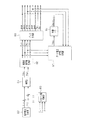
図1に、上記インバータ及びその制御装置の全体構成を示す。 FIG. 1 shows the overall configuration of the inverter and its control device.
図示されるように、3相回転機であるモータ2の3つの相(U相、V相、W相)には、インバータ10が接続されている。このインバータ10は、3相インバータであり、3つの相のそれぞれに対応したスイッチング素子12,14とスイッチング素子16,18とスイッチング素子20,22との並列接続体を備えて構成されている。更に、インバータ10は、各スイッチング素子12〜22に並列に接続されたダイオード24〜34を備えている。そして、スイッチング素子12及びスイッチング素子14を直列接続する接続点がモータ2のU相と接続されている。また、スイッチング素子16及びスイッチング素子18を直列接続する接続点がモータ2のV相と接続されている。更に、スイッチング素子20及びスイッチング素子22を直列接続する接続点がモータ2のW相と接続されている。ちなみに、これらスイッチング素子12〜22は、本実施形態では、絶縁ゲートバイポーラトランジスタ(IGBT)によって構成されている。
As illustrated, an
インバータ10の各1組のスイッチング素子12,14、スイッチング素子16,18、スイッチング素子20,22の両端には、コンデンサ40を介して主電源50の電圧が印加されている。この主電源50は、コンデンサ40の両端に並列接続される一対の直列接続されたスイッチング素子51,52を備えている。これら各スイッチング素子51,52には、それぞれダイオード53,54が並列接続されている。また、スイッチング素子52の両端には、コイル55とコンデンサ56との直列接続体が並列接続されている。更に、コンデンサ56の両端には、バッテリ57が並列接続されている。
The voltage of the
一方、MG−ECU60は、モータ2の出力軸の回転角度を検出する位置センサ62や、U相及びV相に流れる電流を検出する電流センサ64,66、コンデンサ40の両端間の電圧を検出する電圧センサ42の検出結果を取り込む。そして、MG−ECU60は、W相に流れる電流を、キルヒホッフの法則に基づき、U相を流れる電流とV相を流れる電流とから算出する。そして、MG−ECU60は、上記モータ2の出力軸の回転角度や3つの相を流れるそれぞれの電流等に基づき、駆動回路70を介してスイッチング素子12〜22のスイッチング制御を行う。
On the other hand, the MG-ECU 60 detects the voltage between both ends of the position sensor 62 that detects the rotation angle of the output shaft of the
図2に、MG−ECU60の行なう処理についてのブロック線図を示す。 FIG. 2 is a block diagram showing the processing performed by MG-ECU 60.
図2において、変換部80は、上記電流センサ64,66に基づきU相を流れる実電流iuと、V相を流れる実電流ivと、W相を流れる実電流iwとを算出し、これをdq軸に座標変換して実電流id及び実電流iqを生成する部分である。ちなみに、この座標変換に際しては、モータ2の回転角度が用いられるために、変換部80には、位置センサ52によって検出される回転角度θが入力されている。一方、指令電流生成部82は、例えばユーザの加速要求や回転角度θ等に応じて指令電流iqc,idcを生成する部分である。この指令電流iqc,idcは、dq軸上での指令値となっている。
In FIG. 2, the
補償器84は、これら指令電流idcと実電流idとの差と指令電流iqcと実電流iqとの差とに基づき、d軸の指令電圧Vdcとq軸の指令電圧Vqcとを算出する。また、相電圧指令値生成部86は、指令電圧Vdc,Vqcに基づき、3相の指令電圧Vuc、Vvc,Vwcと、コンデンサ40の両端に印加する指令電圧Vhcとを生成する。また、パルス生成部88は、指令電圧Vuc,Vvc,Vwc,Vhcに基づき、スイッチング素子12〜22や、スイッチング素子51,52を操作する操作信号を生成する。詳しくは、U相のスイッチング素子12,14のそれぞれを操作する各操作信号gup,gunと、V相のスイッチング素子16,18のそれぞれを操作する各操作信号gvp,gvnと、W相のスイッチング素子20,22のそれぞれを操作する各操作信号gwp,gwnと、主電源50のスイッチング素子51,52のそれぞれを操作する各操作信号Bp,Bnとを生成する。これら各操作信号gup,gun,gvp,gvn,gwp,gwn,Bp,Bnは、スイッチング素子12〜22,51,52のオン・オフのタイミングを規定する信号である。
The
一方、ゲート電圧指令値生成部90は、補償器84の出力する指令電圧Vdc、Vqcを取り込み、上記スイッチング素子12〜22の各ゲート(導通制御端子)に印加する印加電圧の指令値である指令印加電圧Vgcを生成する。そして、制御IC92は、指令印加電圧Vgcに応じたDutyを有する操作信号Dvを上記駆動回路70に出力する。
On the other hand, the gate voltage command
図3に、上記駆動回路70の回路構成を示す。
FIG. 3 shows a circuit configuration of the
図3では、便宜上、先の図1に示したスイッチング素子12,14を駆動する部分のみを示している。この駆動回路70は、スイッチング素子12,14の各ゲートに電圧を印加する各ドライバ71p,71nを備えている。これら各ドライバ71p,71nは、上記操作信号gup,gunにより駆動される。詳しくは、フォトカプラ72p,72n、駆動IC73p,73nにより電力変換された上記操作信号gup,gunにより駆動される。一方、電圧変換回路74は、スイッチング素子12,14に印加する印加電圧を生成するためのものであり、駆動用電源74a及びコンデンサ74bの両端間にトランス74cの一次側コイルが接続されて構成されている。そして、電圧変換回路74の出力(詳しくはトランス74cの二次側コイルの出力)は、ダイオード75p,75nを介して、ドライバ71p,71nのそれぞれと並列接続されたコンデンサ76p,76nの両端に印加される。
3, for the sake of convenience, only the portion for driving the
こうした構成によれば、先の図2に示した制御IC92から出力される操作信号DvのDutyに応じて電圧変換回路74の出力が制御される。このため、上記Dutyによって、ドライバ71p,71nから出力される電圧を制御することができ、ひいては、スイッチング素子12,14に印加される電圧を制御することができる。
According to such a configuration, the output of the
なお、先の図1に示した駆動回路70は、各相のスイッチング素子16,18や、スイッチング素子20,22毎に、図3に示した各回路を備えており、これら各回路は、MG−ECU60から出力される上記操作信号Dvにより操作される。また、駆動回路70は、上記操作信号Bp,Bnを電力変換してスイッチング素子51,52の各ゲートに印加する回路を更に備えている。
The
図3に示す回路を用いることで、各スイッチング素子12〜22の各ゲートに印加する電圧を可変設定することができる。ここで、ゲート電圧の可変設定について詳述する。
By using the circuit shown in FIG. 3, the voltage applied to each gate of each switching
インバータ10の回路規模を小型化する際には、各スイッチング素子12〜22の発熱が問題となる。この発熱は、各スイッチング素子12〜22における電力損失を主因として生じる。そして、この電力損失は、各スイッチング素子12〜22がオン状態であるときにコレクタからエミッタへと出力される電力の損失(導通損失)と、スイッチング操作に際して生じる電力の損失(スイッチング損失)とに大別される。
When the circuit scale of the
図4(a)に、各スイッチング素子12〜22のオン状態及びオフ状態におけるコレクタ及びエミッタ間の電圧Vceを示し、図4(b)に、コレクタに流入する電流icを示し、図4(c)に、これら電圧Vceと電流icとの積によって定義される電気エネルギの損失を示す。 FIG. 4A shows the voltage Vce between the collector and the emitter in the on state and the off state of each switching element 12-22, FIG. 4B shows the current ic flowing into the collector, and FIG. ) Shows the loss of electric energy defined by the product of the voltage Vce and the current ic.
これら損失を低減するためには、スイッチング素子12〜22をオン状態に維持する際の印加電圧を大きくすることが有効である。これにより、図5に示すように、コレクタ及びエミッタ間の電圧が低下するために、導通損失が低下する。図5では、閾値電圧が「5.8V」であるIGBTを用いて、ゲート印加電圧(ゲート及びエミッタ間の電圧)を「5〜20V」に変化させたときのコレクタ及びエミッタ間電圧Vceを示している。この例では、コレクタ電流icを「400A」としたときに、ゲート印加電圧を「15V」から「20V」に増大させることで、コレクタ及びエミッタ間の電圧Vceは、「0.4V」低減されている。そして、電圧Vceを低減することができれば、導通損失「Vce」も低減される。
In order to reduce these losses, it is effective to increase the applied voltage when maintaining the switching
更に、スイッチング素子12〜22がオン状態であるときの印加電圧を増大させることで、オン状態とオフ状態との間でゲートに印加される電圧差が増大する。そして、この電圧差の増大により、スイッチング損失が低減する。これは、次の理由による。
Further, by increasing the applied voltage when the switching
図6に、先の図3に一点鎖線にて囲った回路についてのオン状態からオフ状態への移行直後の等価回路を示す。この回路は、コンデンサCissと抵抗Rとが直列接続された閉ループ回路である。ここで、コンデンサCissの両電極は、スイッチング素子14のゲート及びエミッタと対応している。この場合、コンデンサCissの両電極間の電圧差Vcissは、その初期値Viを用いて以下の式で表現される。
FIG. 6 shows an equivalent circuit immediately after the transition from the on state to the off state for the circuit surrounded by the one-dot chain line in FIG. This circuit is a closed loop circuit in which a capacitor Ciss and a resistor R are connected in series. Here, both electrodes of the capacitor Ciss correspond to the gate and emitter of the switching
Vciss(t)=Vi×exp{−t/(R×Ciss)}
ここで、初期値Viは、オン状態とオフ状態との間の電圧差となる。このため、この電圧差が大きいほど、ゲート及びエミッタ間の電圧の低下速度が上昇する。これにより、先の図4(c)に示したスイッチング損失も、上記電圧差が増大するほど減少することとなる。
Vciss (t) = Vi × exp {−t / (R × Ciss)}
Here, the initial value Vi is a voltage difference between the on state and the off state. Therefore, the larger the voltage difference, the higher the rate of voltage decrease between the gate and the emitter. As a result, the switching loss shown in FIG. 4C also decreases as the voltage difference increases.
以上から、スイッチング素子12〜22がオン状態であるときの印加電圧を増大させることで、これらスイッチング素子12〜22の損失を低減することができることがわかる。ただし、印加電圧を増大させると、スイッチング素子12〜22の劣化が促進される懸念がある。
From the above, it is understood that the loss of the switching
そこで、本実施形態では、インバータ10の発熱量が多いほど、印加電圧を増大させる。これにより、インバータ10の発熱量の増大の抑制と、スイッチング素子12〜22の劣化の抑制との両立を図る。
Therefore, in the present embodiment, the applied voltage is increased as the amount of heat generated by the
ここで、本実施形態の狙いとするところは、インバータ10の温度上昇(スイッチング素子12〜22)の温度上昇を抑制することにある。このため、所定時間当たりの発熱量を問題とする。これは、同一時間当たりの発熱量が大きいほどインバータ10の温度上昇も大きくなると考えられるからである。
Here, the target of this embodiment is to suppress the temperature rise of the inverter 10 (switching
この所定時間当たりの発熱量が大きいところを先の図4に示した各1回のスイッチング操作における損失によって把握することは極めて困難である。これは、インバータ10から出力される電力が交流であることに鑑みれば、各1回のスイッチング操作における損失の大きさは時々刻々と変化するものであること等による。この所定時間当たりの発熱量が大きいところは、換言すれば、インバータ10の電力損失が大きいところは、一般的には、インバータ10の出力が大きいところとなる。
It is extremely difficult to grasp the large amount of heat generated per predetermined time by the loss in each switching operation shown in FIG. This is because, in view of the fact that the power output from the
図7(a)に、インバータ10の出力とインバータ10の効率(入力電力と出力電力との比)との関係を模式的に示す。一般に、インバータ10は、スイッチング素子12〜22の非線形性等のために、インバータ10の出力が大きいほど電力変換効率が高くなる。しかし、図7(b)に模式的に示すように、一般的には、インバータ10の電力損失は、インバータ10の出力が大きくなるほど大きくなる(ただし、スイッチング周波数一定が前提となる)。
FIG. 7A schematically shows the relationship between the output of the
したがって、インバータ10の電力損失を問題とする場合、一般的には、インバータ10の入力電力や出力電力(出力電力が大きいほど入力電力が大きくなるため)が大きいときを問題とすることとなる。このため、本実施形態では、インバータ10の出力電力が大きいときほど、ゲート印加電圧を大きくする。詳しくは、インバータ10の出力電力が所定以上となるときに、ゲート印加電圧を大きくする。
Therefore, when the power loss of the
以下、図8を用いて、本実施形態においてゲート印加電圧を増大させる領域について説明する。 Hereinafter, a region in which the gate applied voltage is increased in the present embodiment will be described with reference to FIG.
図8は、本実施形態にかかるスイッチング素子12〜22のスイッチング制御の態様を示すものである。図示されるように、モータ2の出力トルクと回転速度によって定義される領域のうち、回転速度が所定以下である領域では周知の正弦波PWMを用いたスイッチング制御がなされる。このPWM制御は、PWM制御を用いてモータ2の各相に正弦波形状の電圧を印加する制御である。これに対し、回転速度が所定以上となると、過変調PWM制御を経て、矩形波弱め界磁制御がなされる。この矩形波制御は、モータ2の各相に矩形波形状の電圧を印加するものである。なお、これら制御については、例えば「日経ものづくり 2004、8月号」に記載されている。
FIG. 8 shows a mode of switching control of the switching
本実施形態では、図8に網掛けをして示す領域において印加電圧を増大させている。すなわち、回転速度が最大となる領域から、トルクが最大であって回転速度の最大側の領域までの領域において、印加電圧が増大されている。これは、この領域がインバータ10の出力が最大となる領域であることによる。
In the present embodiment, the applied voltage is increased in the shaded area in FIG. That is, the applied voltage is increased in the region from the region where the rotational speed is maximum to the region where the torque is maximum and the rotational speed is maximum. This is because this region is a region where the output of the
すなわち、モータ2の出力は「トルク×回転速度」と定義できるため、モータ2の出力は、トルクが大きいほど、また回転速度が大きいほど大きくなる。このため、トルク及び回転速度が最大となる領域において、モータ2の出力は最大となる。一方、モータ2の入力電力、すなわちインバータ10の出力電力は、「モータ2の出力+モータ2内の銅損+モータ2内の鉄損+機械損失」である。このため、モータ2の出力が大きいほど、インバータ10の出力電力も大きくなる傾向にある。更に、モータ2の回転速度が大きくなればなるほど、モータ2の逆起電力が増大するために、回転速度が最大となる領域においても、インバータ10の出力が増大する。
That is, since the output of the
図9に、矩形波制御において、スイッチング周波数が「1.25kHz」であって且つモータ2を流れる電流が「190Arms」であるときについて、オン状態における印加電圧の増大による電力損失の低減効果を示す。図9では、印加電圧を「15V」としたときと「20V」としたときとの電力損失を比較して示した。
FIG. 9 shows the effect of reducing the power loss by increasing the applied voltage in the on state when the switching frequency is “1.25 kHz” and the current flowing through the
ちなみに、先の図8においては、モータ2の出力が最低レベルの領域も、印加電圧を増大させる領域として定義されている。これは、本実施形態では、モータ2の低出力領域においてスイッチング周波数を増大させる制御を行っていることによる。このように、スイッチング周波数が高くなると、スイッチング損失が増大することから、インバータ10の電力損失が大きくなる。このため、本実施形態では、モータ2の低出力領域においても印加電圧を増大させる。
Incidentally, in FIG. 8, the region where the output of the
なお、図8に示す印加電圧の増大領域は、上記指令電圧Vdc,Vqcに基づき、ゲート電圧指令値生成部90によって把握される。すなわち、先の図2に示すように、ゲート電圧指令値生成部90は、指令電圧Vdc,Vqcと指令印加電圧Vgcとの関係を示したマップMを備えて構成されており、これによりゲート印加電圧を可変設定する。
The increase area of the applied voltage shown in FIG. 8 is grasped by the gate voltage command
以上詳述した本実施形態によれば、以下の効果が得られるようになる。 According to the embodiment described in detail above, the following effects can be obtained.
(1)インバータ10の電力損失が所定以上となるとき、オン状態におけるゲート印加電圧を大きくした。これにより、各スイッチング素子12〜22の導通損失とスイッチング損失とを低減することができる。このため、インバータ10の回路規模を抑制しつつも電力損失を低減することができる
(2)指令電圧Vdc,Vqcと指令印加電圧Vgcとの関係を定めるマップを備えることで、MG−ECU60の演算負荷を低減することができる。
(1) When the power loss of the
(第2の実施形態)
以下、第2の実施形態について、先の第1の実施形態との相違点を中心に図面を参照しつつ説明する。
(Second Embodiment)
Hereinafter, the second embodiment will be described with reference to the drawings with a focus on differences from the first embodiment.
本実施形態では、オン状態とオフ状態とで、パワースイッチング素子12〜22のそれぞれのゲートに印加する電圧の符号を逆転させる。
In the present embodiment, the sign of the voltage applied to each gate of the
図10に、本実施形態における上記駆動回路70の構成を示す。図10では、便宜上、スイッチング素子14を駆動する回路部分のみを示している。また、図10では、先の図3に示した部材と同様の機能を有する部材については、便宜上同一の符号を付している。
FIG. 10 shows a configuration of the
図示されるように、ドライバ71nの両端子と並列に、正電源用コンデンサ76pと負電源用コンデンサ76nとの直列接続体が接続されている。また、電圧変換回路74のトランス74dは、2つの2次側コイルの直列接続体を備えており、これらの接続点は、正電源用コンデンサ76p及び負電源用コンデンサ76nの接続点と、フォトカプラ72nの低電位側の端子と、スイッチング素子14のエミッタと接続されている。そして、上記2次側コイルの高電位側の出力は、ダイオード77pを介して正電源用コンデンサ76pの高電位側の端子に印加される。また、2次側コイルの低電位側は、負電源用コンデンサ76nの低電位側からの出力がダイオード77nを介して印加される。
As shown in the figure, a series connection body of a positive power supply capacitor 76p and a negative
こうした構成によれば、オン状態においてはゲート印加電圧(エミッタ及びゲート間電圧)を正電圧として且つ、オフ状態においてはゲート印加電圧を負電圧とすることができる。また、1次側コイルと各2次側コイルとの巻き数比を調整することで、オン状態及びオフ状態における印加電圧の絶対値の比を調整することができる。 According to such a configuration, the gate applied voltage (emitter-gate voltage) can be a positive voltage in the on state, and the gate applied voltage can be a negative voltage in the off state. Moreover, the ratio of the absolute value of the applied voltage in an ON state and an OFF state can be adjusted by adjusting the turns ratio of the primary side coil and each secondary side coil.
図11に、先の図10に一点鎖線で囲った回路について、オン状態からオフ状態への切り替え直後の等価回路を示す。 FIG. 11 shows an equivalent circuit immediately after switching from the on state to the off state for the circuit surrounded by the one-dot chain line in FIG.
この回路は、コンデンサCissと抵抗Rと電圧「−Vn」の負電源とが直列接続された閉ループ回路である。ここで、コンデンサCissの両電極は、スイッチング素子14のゲート及びエミッタと対応している。この場合、コンデンサCissの両電極間の電圧差Vcissは、その初期値Viを用いて以下の式で表現される。
This circuit is a closed loop circuit in which a capacitor Ciss, a resistor R, and a negative power source having a voltage “−Vn” are connected in series. Here, both electrodes of the capacitor Ciss correspond to the gate and emitter of the switching
Vciss(t)=−Vn+Vi×exp{−t/(R×Ciss)}
ここで、初期値Viは、オン状態とオフ状態との間の電圧差となる。このため、この電圧差が大きいほど、ゲート及びエミッタ間の電圧の低下速度が上昇する。そして、本実施形態では、オン状態とオフ状態とで印加電圧の符号が反転するために、初期値Viを大きくすることが可能となる。
Vciss (t) = − Vn + Vi × exp {−t / (R × Ciss)}
Here, the initial value Vi is a voltage difference between the on state and the off state. Therefore, the larger the voltage difference, the higher the rate of voltage decrease between the gate and the emitter. In the present embodiment, since the sign of the applied voltage is inverted between the on state and the off state, the initial value Vi can be increased.
図12に、オン状態からオフ状態への切り替えの前後の印加電圧を「15V」と「0V」とする場合と、「15V」と「−15V」とする場合とについて、先の図6及び図11に示した等価回路を用いて算出される印加電圧の減少速度を示す。図示されるように、「15V」から「−15V」へと切り替える方が、電圧の低下速度が上昇するため、高速スイッチングが可能である。 FIG. 12 shows the case where the applied voltages before and after switching from the on state to the off state are “15V” and “0V”, and the case where the applied voltage is “15V” and “−15V”. 11 shows the decrease rate of the applied voltage calculated using the equivalent circuit shown in FIG. As shown in the figure, switching from “15V” to “−15V” increases the voltage decrease rate, and thus enables high-speed switching.
図13に、ゲート印加電圧が「15V」から「6V」まで低下する時間(放電時間)と、オフ状態の印加電圧との関係を示す。図示されるように、オフ状態における印加電圧の絶対値を増大させることで、換言すればオン状態とオフ状態との間の印加電圧差を増大させることで、電圧の減少速度が上昇する。 FIG. 13 shows the relationship between the time during which the gate applied voltage decreases from “15 V” to “6 V” (discharge time) and the applied voltage in the off state. As illustrated, increasing the absolute value of the applied voltage in the off state, in other words, increasing the applied voltage difference between the on state and the off state increases the voltage reduction rate.
以上から、本実施形態では、オン状態とオフ状態とで印加電圧の符号を反転させることで、オフ状態への移行時間が短縮され、ひいては、スイッチング損失を好適に低減することができる。 From the above, in the present embodiment, by inverting the sign of the applied voltage between the on state and the off state, the transition time to the off state is shortened, and accordingly, the switching loss can be suitably reduced.
以上説明した本実施形態によれば、先の第1の実施形態の上記(1)及び(2)の効果に加えて、更に以下の効果が得られるようになる。 According to the present embodiment described above, the following effects can be obtained in addition to the effects (1) and (2) of the first embodiment.
(3)オン状態とオフ状態とで印加電圧の符号を逆転することで、オン状態とオフ状態との間の印加電圧差を大きくすることができ、スイッチング損失をより好適に低減することができる。 (3) By reversing the sign of the applied voltage between the on state and the off state, the applied voltage difference between the on state and the off state can be increased, and the switching loss can be more suitably reduced. .
(第3の実施形態)
以下、第3の実施形態について、先の第2の実施形態との相違点を中心に図面を参照しつつ説明する。
(Third embodiment)
Hereinafter, the third embodiment will be described with reference to the drawings with a focus on differences from the second embodiment.
本実施形態では、インバータ10の電力損失が大きいときに、その要因に応じてゲート印加電圧の可変制御を行なう。
In this embodiment, when the power loss of the
図14に、本実施形態における上記駆動回路70の構成を示す。図14では、便宜上、スイッチング素子14を駆動する回路部分のみを示している。また、図14では、先の図10に示した部材と同様の機能を有する部材については、便宜上同一の符号を付している。
FIG. 14 shows a configuration of the
本実施形態では、正の印加電圧を生成するための電圧変換回路78と、負の印加電圧を生成するための電圧変換回路79とを備える。そして、電圧変換回路78の2次側コイルの両端は正電源用コンデンサ76pの両端と接続され、電圧変換回路79の2次側コイルの両端は負電源用コンデンサ76nの両端と接続されている。そして、電圧変換回路78を駆動する操作信号Dv1と、電圧変換回路79を駆動する操作信号Dv2とが各別に与えられる。ちなみに、先の図1及び図2においては、操作信号Dvのみしか記載されていないが、本実施形態では、図1及び図2の操作信号Dvに代えて、2つの操作信号Dv1,Dv2を用いる構成とする。
In this embodiment, a
こうした構成において、本実施形態では、電力損失が導通損失によるものかスイッチング損失によるものかに応じて、オン状態とオフ状態とにおける印加電圧の絶対値の比を可変とする。具体的には、図15に示すように、印加電圧の増大領域以外では、オン状態の印加電圧を「15V」とし、オフ状態の印加電圧を「−15V」とする。また、増大領域のうち、モータ2の高出力領域にあっては、導通損失が支配的と考えられるため、オン状態の印加電圧を「20V」とし、オフ状態の印加電圧を「−15V」とする。また、増大領域のうち、モータ2の低出力領域では、スイッチング損失が支配的であるため、オン状態の印加電圧を「15V」とし、オフ状態の印加電圧を「−20V」とする。
In such a configuration, in the present embodiment, the ratio of the absolute values of the applied voltages in the on state and the off state is variable depending on whether the power loss is due to conduction loss or switching loss. Specifically, as shown in FIG. 15, the applied voltage in the on state is set to “15V” and the applied voltage in the off state is set to “−15V” except in the increase region of the applied voltage. Further, in the high output region of the
以上説明した本実施形態によれば、先の第1の実施形態の上記(1)、(2)の効果や、先の第2の実施形態の上記(3)の効果に加えて、更に以下の効果が得られるようになる。 According to this embodiment described above, in addition to the effects (1) and (2) of the previous first embodiment and the effect (3) of the previous second embodiment, The effect will be obtained.
(4)スイッチング素子12〜22の導通損失が大きいときにオン状態における印加電圧を増大し、スイッチング素子12〜22のスイッチング損失が大きいときにオン状態とオフ状態との間の印加電圧の電圧差を大きくした。これにより、電力損失が大きくなるとき、その要因が導通損失であるのか、スイッチング損失であるのかに応じて、印加電圧をより適切に可変制御することができる。
(4) The applied voltage in the on state is increased when the conduction loss of the switching
(第4の実施形態)
以下、第4の実施形態について、先の第1の実施形態との相違点を中心に図面を参照しつつ説明する。
(Fourth embodiment)
Hereinafter, the fourth embodiment will be described with reference to the drawings with a focus on differences from the first embodiment.
本実施形態では、ゲート印加電圧を、モータ2を流れる電流と回転速度とに基づいて可変設定する。図16に、本実施形態にかかるMG−ECU60の行なう処理についてのブロック線図を示す。なお、図16において、先の図2に示したブロックと同様の機能を有するものについては、便宜上同一の符号を付している。
In the present embodiment, the gate application voltage is variably set based on the current flowing through the
図示されるように、ゲート電圧指令値生成部90は、実電流iu,ivと、モータ2の回転角度θとを取り込む。ここで、実電流iu,ivはモータ2のトルクと相関を有するパラメータである。一方、モータ2の回転角度θから、モータ2の回転速度を算出することができる。このため、本実施形態では、ゲート電圧指令値生成部90が、先の図8に示したマップを備えて且つ、実電流iu,ivから算出されるトルクと、回転角度θから算出される回転速度とに基づき、印加電圧を可変設定する。
As illustrated, the gate voltage command
以上説明した本実施形態によっても、先の第1の実施形態の上記(1)及び(2)の効果に準じた効果を得ることができる。 Also according to the present embodiment described above, it is possible to obtain an effect according to the effects (1) and (2) of the first embodiment.
(第5の実施形態)
以下、第5の実施形態について、先の第1の実施形態との相違点を中心に図面を参照しつつ説明する。
(Fifth embodiment)
Hereinafter, a fifth embodiment will be described with reference to the drawings, focusing on differences from the first embodiment.
本実施形態では、指令電圧Vuc,Vvc,Vwcと、スイッチング素子12〜22の操作信号gup,gvp,gwpとに基づき、インバータ10の電力損失が高くなる領域を把握し、これに基づき印加電圧の可変設定を行なう。図17に、本実施形態にかかるMG−ECU60の行なう処理についてのブロック線図を示す。なお、図17において、先の図2に示したブロックと同様の機能を有するものについては、便宜上同一の符号を付している。
In the present embodiment, based on the command voltages Vuc, Vvc, Vwc and the operation signals gup, gvp, gwp of the switching elements 12-22, a region where the power loss of the
図示されるように、ゲート電圧指令値生成部90は、指令電圧Vuc,Vvc,Vwcと、操作信号gup,gvp,gwpとを取り込む。そして、指令電圧Vuc,Vvc,Vwcからモータ2の線間電圧が算出できるため、これに基づきモータ2を流れる電流を把握し、ひいては、各スイッチング素子12〜22を流れる電流を把握する。また、操作信号gup,gvp,gwpに基づきスイッチング周波数を把握する。
As illustrated, the gate voltage command
そして、インバータ10の電力損失(正確にはスイッチング素子12〜22の電力損失)を、以下の態様にて算出する。
a.単位時間当たりの導通損失…各スイッチング素子12〜22を流れる電流に応じて算出される各1回のスイッチングにおける導通損失についての単位時間当たりの時間積分値として算出される。また、これに代えて、単位時間当たりの平均的な導通損失にスイッチング周波数を乗算することで算出してもよい。これは例えば、各相の所定周期の電流平均値に各相のスイッチング周波数を乗算したものについての3相の平均値として算出することができる。
b.単位時間当たりのスイッチング損失…各スイッチング素子12〜22を流れる電流に応じて算出される各1回のスイッチングにおけるスイッチング損失についての単位時間当たりの時間積分値として算出される。また、これに代えて、スイッチング周波数と、各スイッチング素子12〜22を流れる電流の平均値とに基づき算出してもよい。更に、これに代えて、スイッチング周波数を簡易的にスイッチング損失を示すパラメータとしてもよい。
Then, the power loss of the inverter 10 (more precisely, the power loss of the switching
a. Conduction loss per unit time: It is calculated as a time integral value per unit time for the conduction loss in each one-time switching calculated according to the current flowing through each switching element 12-22. Alternatively, it may be calculated by multiplying the average conduction loss per unit time by the switching frequency. This can be calculated, for example, as an average value of three phases for a current average value of each phase in a predetermined cycle multiplied by the switching frequency of each phase.
b. Switching loss per unit time: It is calculated as a time integral value per unit time with respect to the switching loss in each one switching calculated according to the current flowing through each switching element 12-22. Alternatively, it may be calculated based on the switching frequency and the average value of the current flowing through each switching element 12-22. Further, instead of this, the switching frequency may be simply used as a parameter indicating the switching loss.
上記態様にて算出される単位時間当たりの導通損失とスイッチング損失とに基づき、ゲート電圧指令値生成部90により、電力損失が把握される。そして、これにより、印加電圧が可変設定される。
Based on the conduction loss and switching loss per unit time calculated in the above manner, the gate voltage command
以上説明した本実施形態によっても、先の第1の実施形態の上記(1)の効果を得ることができる。 Also according to the present embodiment described above, the effect (1) of the first embodiment can be obtained.
(その他の実施形態)
なお、上記各実施形態は、以下のように変更して実施してもよい。
(Other embodiments)
Each of the above embodiments may be modified as follows.
・先の第4の実施形態では、回転角度θとから算出される回転速度と実電流iu,ivとに基づき指令印加電圧Vgcを算出したがこれに限らない。例えば実電流iu,iv,iwのいずれか1つと回転速度とに基づいて指令印加電圧Vgcを設定してもよい。ただし、この場合、上記いずれか1つの実電流は、略正弦波形状となるため、その大きさが時々刻々変化する。このため、時系列に沿ったサンプリング値の平均値を用いてモータ2のトルクを把握するようにする。
In the fourth embodiment, the command application voltage Vgc is calculated based on the rotation speed calculated from the rotation angle θ and the actual currents iu and iv, but the present invention is not limited to this. For example, the command application voltage Vgc may be set based on any one of the actual currents iu, iv, and iw and the rotation speed. However, in this case, since any one of the actual currents has a substantially sinusoidal shape, the magnitude thereof changes every moment. For this reason, the torque of the
・第5の実施形態において、スイッチング周波数を把握するためのパラメータとしては、上記操作信号gup,gvp,gwpに限らず、操作信号gun,gvn,gwnであってもよい。また、これら6つの操作信号のうちの任意の1つであってもよい。 In the fifth embodiment, the parameters for grasping the switching frequency are not limited to the operation signals “gup”, “gvp”, and “gwp” but may be the operation signals “gun”, “gvn”, and “gwn”. Further, any one of these six operation signals may be used.
・電力損失の算出態様としては、先の第5の実施形態に例示したものに限らない。例えば、電流センサ64,66のいずれか一方の検出値と、電圧センサ42の検出値との積に基づき算出してもよい。すなわち、インバータ10の両端間に印加される電圧(コンデンサ40の両端間電圧)とモータ2を流れる電流との積は、インバータ10の出力電力となるため、これに基づき電力損失を算出することができる。また、電力損失を算出する代わりに、上記2つの値と印加電圧値との関係を示すマップを備えて、上記2つの値から印加電圧を直接設定するようにしてもよい。
-The calculation mode of the power loss is not limited to that illustrated in the fifth embodiment. For example, the calculation may be performed based on the product of the detection value of one of the
また、実電流iu,iv,iwのいずれか1つと、指令電圧Vuc,Vvc,Vwcのうちの上記いずれか1つと対応するものとに基づいて、電力損失を把握してもよい。すなわち、これらの積は特定の相についての瞬間的な電力(電力の時間微分値)となるため、これらの所定時間当たりの積分により特定の相についての電力を算出することができる。そして、各相の対称性により、例えば算出された電力の3倍をインバータ10の電力とすることができる。そして、少なくともインバータ10の出力電力が大きいところを、電力損失が大きいところとすることができる。
Further, the power loss may be grasped based on any one of the actual currents iu, iv, iw and one corresponding to any one of the command voltages Vuc, Vvc, Vwc. That is, since these products are instantaneous power (a time differential value of power) for a specific phase, the power for the specific phase can be calculated by integration per predetermined time. Then, due to the symmetry of each phase, for example, three times the calculated power can be used as the power of the
・第5の実施形態にかかる駆動回路70を、先の図10に示したものや、先の図14に示したものとしてもよい。特に、第5の実施形態においても、インバータ10の電力損失について、それが導通損失によるものかスイッチング損失によりものかを把握することができるため、図14の構成を有することは特に有効である。
The driving
・駆動回路70としては、先の図3、図10、図14において例示したものに限らない。例えば電圧変換回路としてチャージポンプやブーストラップを備えるものであってもよい。
The
・印加電圧を可変設定する際に用いるパラメータとしては、上記各実施形態で例示したものに限らない。例えば先の図2示した補償器84の入力であってもよい。換言すれば、実電流idと指令電流idcとの差と、実電流iqと指令電流iqcとの差とであってもよい。要は、スイッチング制御を行う際に用いるパラメータに基づき、印加電圧を可変設定するものであればよい。すなわち、スイッチング制御を行う際に用いるパラメータによれば、インバータ10の出力電力や、モータ2の出力電力、更には、インバータ10の電力損失そのもの等を把握することができるため、これらに基づき印加電圧を可変設定することができる。
The parameters used when variably setting the applied voltage are not limited to those exemplified in the above embodiments. For example, it may be the input of the
・スイッチング制御手法としては、先の図8で例示したものに限らない。例えば、所定の回転速度領域まではPWM制御を行い、回転速度が所定以上である領域においては瞬時電流値制御を行なうものであってもよい。また、dq変換を行なうものにも限らない。 The switching control method is not limited to that illustrated in FIG. For example, PWM control may be performed up to a predetermined rotation speed region, and instantaneous current value control may be performed in a region where the rotation speed is greater than or equal to a predetermined value. Moreover, it is not restricted to what performs dq conversion.
・導通制御端子への電圧の印加により導通状態が制御される電圧制御形のパワースイッチング素子としては、IGBTに限らない。例えばMOSトランジスタであってもよい。特に、電圧制御形の半導体デバイスにあっては、オン状態における印加電圧(導通端子の電圧を基準とした導通制御端子に印加される電圧)の絶対値を大きくするほど導通損失が増大する傾向等、IGBTと同一の傾向を有するために本発明の適用が有効である。 The voltage control type power switching element whose conduction state is controlled by applying a voltage to the conduction control terminal is not limited to the IGBT. For example, a MOS transistor may be used. In particular, in a voltage-controlled semiconductor device, the conduction loss tends to increase as the absolute value of the applied voltage in the ON state (the voltage applied to the conduction control terminal based on the voltage of the conduction terminal) increases. The present invention is effective because it has the same tendency as the IGBT.
・パワースイッチング素子としては、導通制御端子に論理「H」の電圧を印加することでオン状態となるものに限らない。例えばPチャネルMOSトランジスタのように、論理「L」の電圧を印加することでオン状態となるものであってもよい。この場合であっても、ソース(導通端子)の電圧に対するゲート(導通制御端子)の電圧の差(この場合、負の値)の絶対値を大きくすることで導通損失を低減すること等ができる。 The power switching element is not limited to an element that is turned on by applying a logic “H” voltage to the conduction control terminal. For example, the transistor may be turned on by applying a logic “L” voltage, such as a P-channel MOS transistor. Even in this case, the conduction loss can be reduced by increasing the absolute value of the voltage difference (in this case, a negative value) of the gate (conduction control terminal) with respect to the voltage of the source (conduction terminal). .
・電力変換回路としては、インバータ10に限らない。例えばモータ2に供給する高圧電力を生成するDC−DCコンバータであってもよい。
The power conversion circuit is not limited to the
・電力変換回路としては、ハイブリッド車に搭載されるものに限らない。例えば電気自動車に搭載されるものであってもよい。 -The power conversion circuit is not limited to that installed in a hybrid vehicle. For example, it may be mounted on an electric vehicle.
2…モータ、10…インバータ、12〜22…スイッチング素子、60…ECU、70…駆動回路。
DESCRIPTION OF
Claims (7)
スイッチング周波数を把握するためのパラメータを取り込む手段と、
前記パラメータに基づき、前記パワースイッチング素子のスイッチング周波数の増大により前記スイッチング損失が大きくなる場合に前記パワースイッチング素子のオン状態とオフ状態との間の前記導通制御端子への印加電圧の電圧差を大きくする印加電圧可変手段とを備えることを特徴とする電力変換回路の制御装置。 A power conversion circuit including a voltage-driven power switching element whose conduction state is controlled by applying a voltage to a conduction control terminal, the power switching element for generating output power converted from input power by the power conversion circuit In a control device for a power conversion circuit comprising control means for performing switching control of
Means for capturing parameters for grasping the switching frequency;
Based on the parameter, when the switching loss increases due to an increase in the switching frequency of the power switching element, the voltage difference of the applied voltage to the conduction control terminal between the ON state and the OFF state of the power switching element is increased. A control device for a power conversion circuit, comprising: an applied voltage varying unit that performs the above-described operation.
前記多相回転機の前記スイッチング周波数を増大させる制御を行なう領域が、前記多相回転機のトルク及び回転速度によって定められており、
前記パラメータが、前記電力変換回路の出力電流、前記電力変換回路の出力電圧の少なくとも1つを含むことを特徴とする請求項1〜3のいずれかに記載の電力変換回路の制御装置。 The output power of the power conversion circuit is supplied to a multiphase rotating machine,
A region for performing control to increase the switching frequency of the multi-phase rotating machine is determined by the torque and rotational speed of the multi-phase rotating machine,
The said parameter contains at least 1 of the output current of the said power converter circuit, and the output voltage of the said power converter circuit, The control apparatus of the power converter circuit in any one of Claims 1-3 characterized by the above-mentioned .
前記多相回転機の前記スイッチング周波数を増大させる制御を行なう領域が、前記多相回転機のトルク及び回転速度によって定められており、
前記パラメータが、前記回転機に印加する電圧、前記回転機を流れる電流、前記回転機に印加する指令電圧、前記回転機に流す指令電流、前記回転機の出力軸の回転速度及び前記原動機の出力トルクの少なくとも1つを含むことを特徴とする請求項1〜4のいずれかに記載の電力変換回路の制御装置。 The output power of the power conversion circuit is supplied to a multiphase rotating machine,
A region for performing control to increase the switching frequency of the multi-phase rotating machine is determined by the torque and rotational speed of the multi-phase rotating machine,
The parameters are the voltage applied to the rotating machine, the current flowing through the rotating machine, the command voltage applied to the rotating machine, the command current flowing through the rotating machine, the rotational speed of the output shaft of the rotating machine, and the output of the prime mover. The control device for a power conversion circuit according to claim 1, wherein the control device includes at least one of torques .
前記3相回転機の前記スイッチング周波数を増大させる制御を行なう領域が、前記3相回転機のトルク及び回転速度によって定められており、
前記制御手段は、前記3相の電流がdq軸に変換されたものについての実電流と指令電流との比較に基づき前記スイッチング制御を行うものであり、
前記印加電圧可変手段は、前記パラメータとしてd軸及びq軸の電流及び電圧の少なくとも一方を用いることを特徴とする請求項1〜5のいずれかに記載の電力変換回路の制御装置。 The output power of the power conversion circuit is supplied to each phase of the three-phase rotating machine,
An area for performing control to increase the switching frequency of the three-phase rotating machine is determined by the torque and the rotational speed of the three-phase rotating machine,
The control means performs the switching control based on a comparison between an actual current and a command current for the three-phase current converted into the dq axis.
6. The control apparatus for a power conversion circuit according to claim 1, wherein the applied voltage variable means uses at least one of d-axis and q-axis current and voltage as the parameter .
Priority Applications (2)
| Application Number | Priority Date | Filing Date | Title |
|---|---|---|---|
| JP2005263555A JP4483749B2 (en) | 2005-09-12 | 2005-09-12 | Control device for power conversion circuit |
| US11/519,205 US7558094B2 (en) | 2005-09-12 | 2006-09-12 | Control device for power conversion circuit |
Applications Claiming Priority (1)
| Application Number | Priority Date | Filing Date | Title |
|---|---|---|---|
| JP2005263555A JP4483749B2 (en) | 2005-09-12 | 2005-09-12 | Control device for power conversion circuit |
Publications (2)
| Publication Number | Publication Date |
|---|---|
| JP2007082281A JP2007082281A (en) | 2007-03-29 |
| JP4483749B2 true JP4483749B2 (en) | 2010-06-16 |
Family
ID=37854894
Family Applications (1)
| Application Number | Title | Priority Date | Filing Date |
|---|---|---|---|
| JP2005263555A Active JP4483749B2 (en) | 2005-09-12 | 2005-09-12 | Control device for power conversion circuit |
Country Status (2)
| Country | Link |
|---|---|
| US (1) | US7558094B2 (en) |
| JP (1) | JP4483749B2 (en) |
Families Citing this family (22)
| Publication number | Priority date | Publication date | Assignee | Title |
|---|---|---|---|---|
| JP5109290B2 (en) * | 2006-05-30 | 2012-12-26 | トヨタ自動車株式会社 | Electric motor drive control system and control method thereof |
| DE102007040783A1 (en) * | 2007-08-28 | 2009-03-12 | Conti Temic Microelectronic Gmbh | Method for controlling non-linear load elements |
| JP5266810B2 (en) * | 2008-03-11 | 2013-08-21 | ダイキン工業株式会社 | Power converter |
| US8625315B2 (en) * | 2008-05-09 | 2014-01-07 | Etm Electromatic Inc | Inverter modulator with variable switching frequency |
| JP2013013163A (en) * | 2009-10-30 | 2013-01-17 | Panasonic Corp | Inverter device and induction heating apparatus using the same |
| JP5278298B2 (en) * | 2009-12-17 | 2013-09-04 | 株式会社デンソー | Control device for power conversion circuit |
| JP5126302B2 (en) * | 2010-06-30 | 2013-01-23 | 株式会社安川電機 | 3-level inverter, power conditioner and power generation system |
| JP5511976B2 (en) * | 2010-10-27 | 2014-06-04 | 三菱電機株式会社 | Power converter |
| US8520410B2 (en) * | 2010-11-09 | 2013-08-27 | Flextronics Ap, Llc | Virtual parametric high side MOSFET driver |
| FR2980318B1 (en) * | 2011-09-16 | 2017-06-09 | Valeo Systemes De Controle Moteur | METHOD OF REDUCING COMMON MODE CURRENT |
| JP5639978B2 (en) | 2011-09-27 | 2014-12-10 | 日立オートモティブシステムズ株式会社 | Automotive power conversion control device |
| KR101301221B1 (en) | 2012-07-20 | 2013-08-28 | 엘에스파워세미텍 주식회사 | Power circuit and power module for 3 phase motor driving |
| JP2013013325A (en) * | 2012-10-19 | 2013-01-17 | Daikin Ind Ltd | Power conversion apparatus |
| JP6295782B2 (en) * | 2014-03-31 | 2018-03-20 | 株式会社安川電機 | Power conversion device, power generation system, control device, and power conversion method |
| CN105320204B (en) * | 2014-06-05 | 2018-06-22 | 成都市东和兴科节能技术研究所 | A kind of five notch power control device of three-phase electric appliance |
| JP6217667B2 (en) * | 2015-02-19 | 2017-10-25 | 株式会社豊田自動織機 | Electric compressor |
| US20180096088A1 (en) * | 2016-09-30 | 2018-04-05 | Taiyo Yuden Co., Ltd. | Method of constructing and method of simulating equivalent circuit for capacitor, and simulation device therefor |
| EP3621545B1 (en) | 2017-05-10 | 2024-02-21 | MAKO Surgical Corp. | Robotic spine surgery system |
| US11033341B2 (en) | 2017-05-10 | 2021-06-15 | Mako Surgical Corp. | Robotic spine surgery system and methods |
| EP3447895B1 (en) | 2017-08-21 | 2024-04-03 | Flex, Ltd. | Adaptive resonant frequency converter |
| CN111641256B (en) | 2019-03-01 | 2024-10-22 | 弗莱克斯有限公司 | Automatic AC Feed Control (AFC) with zero voltage/current switching |
| US11004591B2 (en) | 2019-04-17 | 2021-05-11 | Flex Ltd. | Multilayer transformer structure comprising multiple rectification elements |
Family Cites Families (12)
| Publication number | Priority date | Publication date | Assignee | Title |
|---|---|---|---|---|
| JP3675014B2 (en) | 1995-06-08 | 2005-07-27 | 株式会社デンソー | Inverter control device |
| JP3050138B2 (en) * | 1996-09-13 | 2000-06-12 | トヨタ自動車株式会社 | Power output device and control method thereof |
| JPH11113283A (en) * | 1997-09-30 | 1999-04-23 | Toshiba Corp | Motor driver |
| JP4460708B2 (en) * | 2000-03-29 | 2010-05-12 | 株式会社東芝 | Permanent magnet motor control device that combines engine starter and generator |
| JP3965934B2 (en) * | 2001-05-09 | 2007-08-29 | 株式会社日立製作所 | Moving body control device and moving body system |
| JP3867518B2 (en) * | 2001-06-06 | 2007-01-10 | 株式会社日立製作所 | Sensorless control system for synchronous motor |
| JP4032879B2 (en) | 2001-10-25 | 2008-01-16 | 富士電機デバイステクノロジー株式会社 | Drive circuit and drive method |
| JP2004015910A (en) | 2002-06-06 | 2004-01-15 | Fuji Electric Holdings Co Ltd | Gate drive circuit |
| JP2004064822A (en) | 2002-07-25 | 2004-02-26 | Fuji Electric Holdings Co Ltd | Driving method for voltage driving type semiconductor element |
| JP2004096830A (en) | 2002-08-29 | 2004-03-25 | Fuji Electric Holdings Co Ltd | Driving method of voltage-driven semiconductor element |
| JP2004222420A (en) | 2003-01-15 | 2004-08-05 | Kokusan Denki Co Ltd | Motor drive |
| JP4044861B2 (en) * | 2003-04-03 | 2008-02-06 | 三菱電機株式会社 | Power conversion device and power conversion system device including the power conversion device |
-
2005
- 2005-09-12 JP JP2005263555A patent/JP4483749B2/en active Active
-
2006
- 2006-09-12 US US11/519,205 patent/US7558094B2/en active Active
Also Published As
| Publication number | Publication date |
|---|---|
| US20070058406A1 (en) | 2007-03-15 |
| US7558094B2 (en) | 2009-07-07 |
| JP2007082281A (en) | 2007-03-29 |
Similar Documents
| Publication | Publication Date | Title |
|---|---|---|
| JP4483749B2 (en) | Control device for power conversion circuit | |
| JP4379427B2 (en) | Control device for multiphase rotating electrical machine | |
| US8278865B2 (en) | Control device | |
| WO2011135696A1 (en) | Power conversion device | |
| JP5633650B2 (en) | Vehicle and vehicle control method | |
| WO2011099122A1 (en) | Power conversion device | |
| US11489474B2 (en) | Driving device for rotating electric machine | |
| JP2009291019A (en) | Controller for inverter for ac motor | |
| US20130038140A1 (en) | Switching circuit | |
| JP6218906B1 (en) | Power converter | |
| JP2014171362A (en) | Power conversion apparatus | |
| JP2013055852A (en) | Driver of ac motor and vehicle with the same, and control method of ac motor | |
| JP5955761B2 (en) | Vehicle control device | |
| JP2011155788A (en) | Power supply system | |
| JP4957574B2 (en) | Rotating machine control device and rotating machine control system | |
| JP2013090350A (en) | Power conversion apparatus | |
| JP5549337B2 (en) | Motor generator drive device and vehicle drive system | |
| JP6776961B2 (en) | Inverter control device and inverter control method | |
| JP7316194B2 (en) | Drive system controller | |
| JP5290048B2 (en) | Vehicle motor control system | |
| JP6880866B2 (en) | Inverter control device and inverter control method | |
| JP2009171641A (en) | Drive unit of motor | |
| JP5402093B2 (en) | Power converter | |
| JP2010220306A (en) | Motor control equipment | |
| JP5975797B2 (en) | Power converter |
Legal Events
| Date | Code | Title | Description |
|---|---|---|---|
| A621 | Written request for application examination |
Free format text: JAPANESE INTERMEDIATE CODE: A621 Effective date: 20071009 |
|
| A131 | Notification of reasons for refusal |
Free format text: JAPANESE INTERMEDIATE CODE: A131 Effective date: 20090710 |
|
| A521 | Request for written amendment filed |
Free format text: JAPANESE INTERMEDIATE CODE: A523 Effective date: 20090904 |
|
| A131 | Notification of reasons for refusal |
Free format text: JAPANESE INTERMEDIATE CODE: A131 Effective date: 20091104 |
|
| A521 | Request for written amendment filed |
Free format text: JAPANESE INTERMEDIATE CODE: A523 Effective date: 20091224 |
|
| TRDD | Decision of grant or rejection written | ||
| A01 | Written decision to grant a patent or to grant a registration (utility model) |
Free format text: JAPANESE INTERMEDIATE CODE: A01 Effective date: 20100302 |
|
| A01 | Written decision to grant a patent or to grant a registration (utility model) |
Free format text: JAPANESE INTERMEDIATE CODE: A01 |
|
| A61 | First payment of annual fees (during grant procedure) |
Free format text: JAPANESE INTERMEDIATE CODE: A61 Effective date: 20100315 |
|
| R151 | Written notification of patent or utility model registration |
Ref document number: 4483749 Country of ref document: JP Free format text: JAPANESE INTERMEDIATE CODE: R151 |
|
| FPAY | Renewal fee payment (event date is renewal date of database) |
Free format text: PAYMENT UNTIL: 20130402 Year of fee payment: 3 |
|
| FPAY | Renewal fee payment (event date is renewal date of database) |
Free format text: PAYMENT UNTIL: 20130402 Year of fee payment: 3 |
|
| FPAY | Renewal fee payment (event date is renewal date of database) |
Free format text: PAYMENT UNTIL: 20140402 Year of fee payment: 4 |
|
| R250 | Receipt of annual fees |
Free format text: JAPANESE INTERMEDIATE CODE: R250 |
|
| R250 | Receipt of annual fees |
Free format text: JAPANESE INTERMEDIATE CODE: R250 |
|
| R250 | Receipt of annual fees |
Free format text: JAPANESE INTERMEDIATE CODE: R250 |
|
| R250 | Receipt of annual fees |
Free format text: JAPANESE INTERMEDIATE CODE: R250 |
|
| R250 | Receipt of annual fees |
Free format text: JAPANESE INTERMEDIATE CODE: R250 |
|
| R250 | Receipt of annual fees |
Free format text: JAPANESE INTERMEDIATE CODE: R250 |
|
| R250 | Receipt of annual fees |
Free format text: JAPANESE INTERMEDIATE CODE: R250 |
|
| R250 | Receipt of annual fees |
Free format text: JAPANESE INTERMEDIATE CODE: R250 |
|
| R250 | Receipt of annual fees |
Free format text: JAPANESE INTERMEDIATE CODE: R250 |
|
| R250 | Receipt of annual fees |
Free format text: JAPANESE INTERMEDIATE CODE: R250 |
|
| R250 | Receipt of annual fees |
Free format text: JAPANESE INTERMEDIATE CODE: R250 |