JP4408713B2 - 半導体装置の製造方法 - Google Patents
半導体装置の製造方法 Download PDFInfo
- Publication number
- JP4408713B2 JP4408713B2 JP2004026666A JP2004026666A JP4408713B2 JP 4408713 B2 JP4408713 B2 JP 4408713B2 JP 2004026666 A JP2004026666 A JP 2004026666A JP 2004026666 A JP2004026666 A JP 2004026666A JP 4408713 B2 JP4408713 B2 JP 4408713B2
- Authority
- JP
- Japan
- Prior art keywords
- film
- silicon
- semiconductor device
- silicon nitride
- nitride film
- Prior art date
- Legal status (The legal status is an assumption and is not a legal conclusion. Google has not performed a legal analysis and makes no representation as to the accuracy of the status listed.)
- Expired - Fee Related
Links
- 239000004065 semiconductor Substances 0.000 title claims description 61
- 238000004519 manufacturing process Methods 0.000 title claims description 25
- 239000000758 substrate Substances 0.000 claims description 67
- 229910052581 Si3N4 Inorganic materials 0.000 claims description 43
- HQVNEWCFYHHQES-UHFFFAOYSA-N silicon nitride Chemical compound N12[Si]34N5[Si]62N3[Si]51N64 HQVNEWCFYHHQES-UHFFFAOYSA-N 0.000 claims description 43
- 238000005268 plasma chemical vapour deposition Methods 0.000 claims description 16
- 239000000853 adhesive Substances 0.000 claims description 14
- 230000001070 adhesive effect Effects 0.000 claims description 14
- 239000004020 conductor Substances 0.000 claims description 11
- 230000015572 biosynthetic process Effects 0.000 claims description 10
- 238000000227 grinding Methods 0.000 claims description 9
- 229910052710 silicon Inorganic materials 0.000 description 65
- 239000010703 silicon Substances 0.000 description 65
- 238000000034 method Methods 0.000 description 54
- XUIMIQQOPSSXEZ-UHFFFAOYSA-N Silicon Chemical compound [Si] XUIMIQQOPSSXEZ-UHFFFAOYSA-N 0.000 description 51
- 239000007789 gas Substances 0.000 description 16
- VYPSYNLAJGMNEJ-UHFFFAOYSA-N Silicium dioxide Chemical compound O=[Si]=O VYPSYNLAJGMNEJ-UHFFFAOYSA-N 0.000 description 13
- 229910052814 silicon oxide Inorganic materials 0.000 description 13
- 239000012495 reaction gas Substances 0.000 description 9
- 239000011347 resin Substances 0.000 description 9
- 229920005989 resin Polymers 0.000 description 9
- 229910008045 Si-Si Inorganic materials 0.000 description 8
- 229910006411 Si—Si Inorganic materials 0.000 description 8
- 239000011229 interlayer Substances 0.000 description 8
- 239000011248 coating agent Substances 0.000 description 7
- 238000000576 coating method Methods 0.000 description 7
- 229910052751 metal Inorganic materials 0.000 description 6
- 239000002184 metal Substances 0.000 description 6
- 230000000149 penetrating effect Effects 0.000 description 6
- 238000005229 chemical vapour deposition Methods 0.000 description 4
- 238000006243 chemical reaction Methods 0.000 description 3
- 238000007796 conventional method Methods 0.000 description 3
- 230000007547 defect Effects 0.000 description 3
- 238000001312 dry etching Methods 0.000 description 3
- 230000000694 effects Effects 0.000 description 3
- 229910000679 solder Inorganic materials 0.000 description 3
- 238000004544 sputter deposition Methods 0.000 description 3
- 238000001039 wet etching Methods 0.000 description 3
- 238000005033 Fourier transform infrared spectroscopy Methods 0.000 description 2
- 230000004888 barrier function Effects 0.000 description 2
- 238000010586 diagram Methods 0.000 description 2
- 238000005530 etching Methods 0.000 description 2
- 239000011521 glass Substances 0.000 description 2
- 239000010410 layer Substances 0.000 description 2
- 238000005259 measurement Methods 0.000 description 2
- 239000012528 membrane Substances 0.000 description 2
- 239000000203 mixture Substances 0.000 description 2
- 150000004767 nitrides Chemical class 0.000 description 2
- 238000007747 plating Methods 0.000 description 2
- 238000005498 polishing Methods 0.000 description 2
- 229920001721 polyimide Polymers 0.000 description 2
- 230000003014 reinforcing effect Effects 0.000 description 2
- WFKWXMTUELFFGS-UHFFFAOYSA-N tungsten Chemical compound [W] WFKWXMTUELFFGS-UHFFFAOYSA-N 0.000 description 2
- 239000010937 tungsten Substances 0.000 description 2
- 229910052721 tungsten Inorganic materials 0.000 description 2
- RZVAJINKPMORJF-UHFFFAOYSA-N Acetaminophen Chemical compound CC(=O)NC1=CC=C(O)C=C1 RZVAJINKPMORJF-UHFFFAOYSA-N 0.000 description 1
- ZOKXTWBITQBERF-UHFFFAOYSA-N Molybdenum Chemical compound [Mo] ZOKXTWBITQBERF-UHFFFAOYSA-N 0.000 description 1
- ATJFFYVFTNAWJD-UHFFFAOYSA-N Tin Chemical compound [Sn] ATJFFYVFTNAWJD-UHFFFAOYSA-N 0.000 description 1
- 238000010521 absorption reaction Methods 0.000 description 1
- 238000004380 ashing Methods 0.000 description 1
- QVGXLLKOCUKJST-UHFFFAOYSA-N atomic oxygen Chemical compound [O] QVGXLLKOCUKJST-UHFFFAOYSA-N 0.000 description 1
- 238000006482 condensation reaction Methods 0.000 description 1
- 230000018044 dehydration Effects 0.000 description 1
- 238000006297 dehydration reaction Methods 0.000 description 1
- 238000000151 deposition Methods 0.000 description 1
- 238000011161 development Methods 0.000 description 1
- 238000009713 electroplating Methods 0.000 description 1
- 238000002474 experimental method Methods 0.000 description 1
- 125000004435 hydrogen atom Chemical group [H]* 0.000 description 1
- 238000009413 insulation Methods 0.000 description 1
- 238000010849 ion bombardment Methods 0.000 description 1
- 150000002500 ions Chemical class 0.000 description 1
- 230000001678 irradiating effect Effects 0.000 description 1
- 238000004518 low pressure chemical vapour deposition Methods 0.000 description 1
- 230000007257 malfunction Effects 0.000 description 1
- 239000000463 material Substances 0.000 description 1
- 229910052750 molybdenum Inorganic materials 0.000 description 1
- 239000011733 molybdenum Substances 0.000 description 1
- 230000003287 optical effect Effects 0.000 description 1
- 230000003647 oxidation Effects 0.000 description 1
- 238000007254 oxidation reaction Methods 0.000 description 1
- 239000001301 oxygen Substances 0.000 description 1
- 229910052760 oxygen Inorganic materials 0.000 description 1
- 238000000206 photolithography Methods 0.000 description 1
- 239000005297 pyrex Substances 0.000 description 1
- 238000006748 scratching Methods 0.000 description 1
- 230000002393 scratching effect Effects 0.000 description 1
- 229910021332 silicide Inorganic materials 0.000 description 1
- FVBUAEGBCNSCDD-UHFFFAOYSA-N silicide(4-) Chemical compound [Si-4] FVBUAEGBCNSCDD-UHFFFAOYSA-N 0.000 description 1
- 239000002356 single layer Substances 0.000 description 1
- 238000001228 spectrum Methods 0.000 description 1
- 239000000126 substance Substances 0.000 description 1
- 239000002344 surface layer Substances 0.000 description 1
- 238000009864 tensile test Methods 0.000 description 1
Images


Classifications
-
- H—ELECTRICITY
- H01—ELECTRIC ELEMENTS
- H01L—SEMICONDUCTOR DEVICES NOT COVERED BY CLASS H10
- H01L21/00—Processes or apparatus adapted for the manufacture or treatment of semiconductor or solid state devices or of parts thereof
- H01L21/02—Manufacture or treatment of semiconductor devices or of parts thereof
- H01L21/027—Making masks on semiconductor bodies for further photolithographic processing not provided for in group H01L21/18 or H01L21/34
- H01L21/033—Making masks on semiconductor bodies for further photolithographic processing not provided for in group H01L21/18 or H01L21/34 comprising inorganic layers
- H01L21/0334—Making masks on semiconductor bodies for further photolithographic processing not provided for in group H01L21/18 or H01L21/34 comprising inorganic layers characterised by their size, orientation, disposition, behaviour, shape, in horizontal or vertical plane
- H01L21/0337—Making masks on semiconductor bodies for further photolithographic processing not provided for in group H01L21/18 or H01L21/34 comprising inorganic layers characterised by their size, orientation, disposition, behaviour, shape, in horizontal or vertical plane characterised by the process involved to create the mask, e.g. lift-off masks, sidewalls, or to modify the mask, e.g. pre-treatment, post-treatment
-
- H—ELECTRICITY
- H01—ELECTRIC ELEMENTS
- H01L—SEMICONDUCTOR DEVICES NOT COVERED BY CLASS H10
- H01L21/00—Processes or apparatus adapted for the manufacture or treatment of semiconductor or solid state devices or of parts thereof
- H01L21/02—Manufacture or treatment of semiconductor devices or of parts thereof
- H01L21/04—Manufacture or treatment of semiconductor devices or of parts thereof the devices having potential barriers, e.g. a PN junction, depletion layer or carrier concentration layer
- H01L21/18—Manufacture or treatment of semiconductor devices or of parts thereof the devices having potential barriers, e.g. a PN junction, depletion layer or carrier concentration layer the devices having semiconductor bodies comprising elements of Group IV of the Periodic Table or AIIIBV compounds with or without impurities, e.g. doping materials
- H01L21/30—Treatment of semiconductor bodies using processes or apparatus not provided for in groups H01L21/20 - H01L21/26
- H01L21/31—Treatment of semiconductor bodies using processes or apparatus not provided for in groups H01L21/20 - H01L21/26 to form insulating layers thereon, e.g. for masking or by using photolithographic techniques; After treatment of these layers; Selection of materials for these layers
- H01L21/314—Inorganic layers
- H01L21/318—Inorganic layers composed of nitrides
- H01L21/3185—Inorganic layers composed of nitrides of siliconnitrides
-
- H—ELECTRICITY
- H01—ELECTRIC ELEMENTS
- H01L—SEMICONDUCTOR DEVICES NOT COVERED BY CLASS H10
- H01L21/00—Processes or apparatus adapted for the manufacture or treatment of semiconductor or solid state devices or of parts thereof
- H01L21/70—Manufacture or treatment of devices consisting of a plurality of solid state components formed in or on a common substrate or of parts thereof; Manufacture of integrated circuit devices or of parts thereof
- H01L21/71—Manufacture of specific parts of devices defined in group H01L21/70
- H01L21/768—Applying interconnections to be used for carrying current between separate components within a device comprising conductors and dielectrics
- H01L21/76898—Applying interconnections to be used for carrying current between separate components within a device comprising conductors and dielectrics formed through a semiconductor substrate
-
- H—ELECTRICITY
- H01—ELECTRIC ELEMENTS
- H01L—SEMICONDUCTOR DEVICES NOT COVERED BY CLASS H10
- H01L23/00—Details of semiconductor or other solid state devices
- H01L23/12—Mountings, e.g. non-detachable insulating substrates
- H01L23/14—Mountings, e.g. non-detachable insulating substrates characterised by the material or its electrical properties
- H01L23/147—Semiconductor insulating substrates
-
- H—ELECTRICITY
- H01—ELECTRIC ELEMENTS
- H01L—SEMICONDUCTOR DEVICES NOT COVERED BY CLASS H10
- H01L23/00—Details of semiconductor or other solid state devices
- H01L23/48—Arrangements for conducting electric current to or from the solid state body in operation, e.g. leads, terminal arrangements ; Selection of materials therefor
- H01L23/488—Arrangements for conducting electric current to or from the solid state body in operation, e.g. leads, terminal arrangements ; Selection of materials therefor consisting of soldered or bonded constructions
- H01L23/498—Leads, i.e. metallisations or lead-frames on insulating substrates, e.g. chip carriers
- H01L23/49827—Via connections through the substrates, e.g. pins going through the substrate, coaxial cables
-
- H—ELECTRICITY
- H01—ELECTRIC ELEMENTS
- H01L—SEMICONDUCTOR DEVICES NOT COVERED BY CLASS H10
- H01L21/00—Processes or apparatus adapted for the manufacture or treatment of semiconductor or solid state devices or of parts thereof
- H01L21/02—Manufacture or treatment of semiconductor devices or of parts thereof
- H01L21/02104—Forming layers
- H01L21/02107—Forming insulating materials on a substrate
- H01L21/02109—Forming insulating materials on a substrate characterised by the type of layer, e.g. type of material, porous/non-porous, pre-cursors, mixtures or laminates
- H01L21/02112—Forming insulating materials on a substrate characterised by the type of layer, e.g. type of material, porous/non-porous, pre-cursors, mixtures or laminates characterised by the material of the layer
- H01L21/02123—Forming insulating materials on a substrate characterised by the type of layer, e.g. type of material, porous/non-porous, pre-cursors, mixtures or laminates characterised by the material of the layer the material containing silicon
- H01L21/02164—Forming insulating materials on a substrate characterised by the type of layer, e.g. type of material, porous/non-porous, pre-cursors, mixtures or laminates characterised by the material of the layer the material containing silicon the material being a silicon oxide, e.g. SiO2
-
- H—ELECTRICITY
- H01—ELECTRIC ELEMENTS
- H01L—SEMICONDUCTOR DEVICES NOT COVERED BY CLASS H10
- H01L21/00—Processes or apparatus adapted for the manufacture or treatment of semiconductor or solid state devices or of parts thereof
- H01L21/02—Manufacture or treatment of semiconductor devices or of parts thereof
- H01L21/02104—Forming layers
- H01L21/02107—Forming insulating materials on a substrate
- H01L21/02109—Forming insulating materials on a substrate characterised by the type of layer, e.g. type of material, porous/non-porous, pre-cursors, mixtures or laminates
- H01L21/02112—Forming insulating materials on a substrate characterised by the type of layer, e.g. type of material, porous/non-porous, pre-cursors, mixtures or laminates characterised by the material of the layer
- H01L21/02123—Forming insulating materials on a substrate characterised by the type of layer, e.g. type of material, porous/non-porous, pre-cursors, mixtures or laminates characterised by the material of the layer the material containing silicon
- H01L21/0217—Forming insulating materials on a substrate characterised by the type of layer, e.g. type of material, porous/non-porous, pre-cursors, mixtures or laminates characterised by the material of the layer the material containing silicon the material being a silicon nitride not containing oxygen, e.g. SixNy or SixByNz
-
- H—ELECTRICITY
- H01—ELECTRIC ELEMENTS
- H01L—SEMICONDUCTOR DEVICES NOT COVERED BY CLASS H10
- H01L21/00—Processes or apparatus adapted for the manufacture or treatment of semiconductor or solid state devices or of parts thereof
- H01L21/02—Manufacture or treatment of semiconductor devices or of parts thereof
- H01L21/02104—Forming layers
- H01L21/02107—Forming insulating materials on a substrate
- H01L21/02225—Forming insulating materials on a substrate characterised by the process for the formation of the insulating layer
- H01L21/0226—Forming insulating materials on a substrate characterised by the process for the formation of the insulating layer formation by a deposition process
- H01L21/02263—Forming insulating materials on a substrate characterised by the process for the formation of the insulating layer formation by a deposition process deposition from the gas or vapour phase
- H01L21/02271—Forming insulating materials on a substrate characterised by the process for the formation of the insulating layer formation by a deposition process deposition from the gas or vapour phase deposition by decomposition or reaction of gaseous or vapour phase compounds, i.e. chemical vapour deposition
- H01L21/02274—Forming insulating materials on a substrate characterised by the process for the formation of the insulating layer formation by a deposition process deposition from the gas or vapour phase deposition by decomposition or reaction of gaseous or vapour phase compounds, i.e. chemical vapour deposition in the presence of a plasma [PECVD]
-
- H—ELECTRICITY
- H01—ELECTRIC ELEMENTS
- H01L—SEMICONDUCTOR DEVICES NOT COVERED BY CLASS H10
- H01L2224/00—Indexing scheme for arrangements for connecting or disconnecting semiconductor or solid-state bodies and methods related thereto as covered by H01L24/00
- H01L2224/01—Means for bonding being attached to, or being formed on, the surface to be connected, e.g. chip-to-package, die-attach, "first-level" interconnects; Manufacturing methods related thereto
- H01L2224/02—Bonding areas; Manufacturing methods related thereto
- H01L2224/04—Structure, shape, material or disposition of the bonding areas prior to the connecting process
- H01L2224/05—Structure, shape, material or disposition of the bonding areas prior to the connecting process of an individual bonding area
- H01L2224/0554—External layer
- H01L2224/05573—Single external layer
-
- H—ELECTRICITY
- H01—ELECTRIC ELEMENTS
- H01L—SEMICONDUCTOR DEVICES NOT COVERED BY CLASS H10
- H01L2224/00—Indexing scheme for arrangements for connecting or disconnecting semiconductor or solid-state bodies and methods related thereto as covered by H01L24/00
- H01L2224/01—Means for bonding being attached to, or being formed on, the surface to be connected, e.g. chip-to-package, die-attach, "first-level" interconnects; Manufacturing methods related thereto
- H01L2224/10—Bump connectors; Manufacturing methods related thereto
- H01L2224/15—Structure, shape, material or disposition of the bump connectors after the connecting process
- H01L2224/16—Structure, shape, material or disposition of the bump connectors after the connecting process of an individual bump connector
- H01L2224/161—Disposition
- H01L2224/16135—Disposition the bump connector connecting between different semiconductor or solid-state bodies, i.e. chip-to-chip
- H01L2224/16145—Disposition the bump connector connecting between different semiconductor or solid-state bodies, i.e. chip-to-chip the bodies being stacked
- H01L2224/16146—Disposition the bump connector connecting between different semiconductor or solid-state bodies, i.e. chip-to-chip the bodies being stacked the bump connector connecting to a via connection in the semiconductor or solid-state body
-
- H—ELECTRICITY
- H01—ELECTRIC ELEMENTS
- H01L—SEMICONDUCTOR DEVICES NOT COVERED BY CLASS H10
- H01L24/00—Arrangements for connecting or disconnecting semiconductor or solid-state bodies; Methods or apparatus related thereto
- H01L24/01—Means for bonding being attached to, or being formed on, the surface to be connected, e.g. chip-to-package, die-attach, "first-level" interconnects; Manufacturing methods related thereto
- H01L24/02—Bonding areas ; Manufacturing methods related thereto
- H01L24/04—Structure, shape, material or disposition of the bonding areas prior to the connecting process
- H01L24/05—Structure, shape, material or disposition of the bonding areas prior to the connecting process of an individual bonding area
-
- H—ELECTRICITY
- H01—ELECTRIC ELEMENTS
- H01L—SEMICONDUCTOR DEVICES NOT COVERED BY CLASS H10
- H01L24/00—Arrangements for connecting or disconnecting semiconductor or solid-state bodies; Methods or apparatus related thereto
- H01L24/01—Means for bonding being attached to, or being formed on, the surface to be connected, e.g. chip-to-package, die-attach, "first-level" interconnects; Manufacturing methods related thereto
- H01L24/10—Bump connectors ; Manufacturing methods related thereto
- H01L24/15—Structure, shape, material or disposition of the bump connectors after the connecting process
- H01L24/16—Structure, shape, material or disposition of the bump connectors after the connecting process of an individual bump connector
-
- H—ELECTRICITY
- H01—ELECTRIC ELEMENTS
- H01L—SEMICONDUCTOR DEVICES NOT COVERED BY CLASS H10
- H01L2924/00—Indexing scheme for arrangements or methods for connecting or disconnecting semiconductor or solid-state bodies as covered by H01L24/00
- H01L2924/0001—Technical content checked by a classifier
- H01L2924/00014—Technical content checked by a classifier the subject-matter covered by the group, the symbol of which is combined with the symbol of this group, being disclosed without further technical details
-
- H—ELECTRICITY
- H01—ELECTRIC ELEMENTS
- H01L—SEMICONDUCTOR DEVICES NOT COVERED BY CLASS H10
- H01L2924/00—Indexing scheme for arrangements or methods for connecting or disconnecting semiconductor or solid-state bodies as covered by H01L24/00
- H01L2924/10—Details of semiconductor or other solid state devices to be connected
- H01L2924/11—Device type
- H01L2924/13—Discrete devices, e.g. 3 terminal devices
- H01L2924/1304—Transistor
- H01L2924/1306—Field-effect transistor [FET]
- H01L2924/13091—Metal-Oxide-Semiconductor Field-Effect Transistor [MOSFET]
Landscapes
- Engineering & Computer Science (AREA)
- Physics & Mathematics (AREA)
- Condensed Matter Physics & Semiconductors (AREA)
- General Physics & Mathematics (AREA)
- Computer Hardware Design (AREA)
- Microelectronics & Electronic Packaging (AREA)
- Power Engineering (AREA)
- Manufacturing & Machinery (AREA)
- Chemical & Material Sciences (AREA)
- Inorganic Chemistry (AREA)
- Internal Circuitry In Semiconductor Integrated Circuit Devices (AREA)
Description

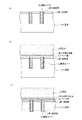
2 第1絶縁膜
3 第2絶縁膜
4 孔
5 導電材料
5a 導電性プラグ
6 コーティング膜
7 紫外線硬化樹脂
8 支持体
9 シリコン窒化膜
10 第1の層間絶縁膜
11 マスクパターン
12 積層絶縁膜
13 多層配線構造
14 パッド
15 シリコン酸化膜
16 半田バンプ
17 他の半導体チップ
18 スクラッチ
Claims (2)
- 半導体基板の一方の面に所定の深さの孔を形成する工程と、
前記孔の内部に絶縁膜を介して導電材料を埋設して導電性プラグを形成する工程と、
前記半導体基板の前記一方の面に、接着剤を用いて支持部材を固定する工程と、
前記半導体基板の他方の面を、前記導電性プラグが突出するまで研削する工程と、
前記他方の面に、単一周波数の平行平板型プラズマCVD法を用い、成膜用ガスとしてSiH 4 、NH 3 及びN 2 を含む混合ガスを用いて、前記支持部材を固定可能な前記接着剤の耐熱温度以下の成膜温度でシリコン窒化膜を形成する工程と、
前記導電性プラグ表面の前記シリコン窒化膜を研削する工程と、
前記半導体基板から前記支持部材を取り外す工程と、を少なくとも有することを特徴とする半導体装置の製造方法。 - 前記シリコン窒化膜を、100℃以下の温度で成膜すること特徴とする請求項1記載の半導体装置の製造方法。
Priority Applications (3)
| Application Number | Priority Date | Filing Date | Title |
|---|---|---|---|
| JP2004026666A JP4408713B2 (ja) | 2004-02-03 | 2004-02-03 | 半導体装置の製造方法 |
| US11/047,576 US7291911B2 (en) | 2004-02-03 | 2005-02-02 | Semiconductor device and manufacturing method thereof |
| US11/892,923 US7488674B2 (en) | 2004-02-03 | 2007-08-28 | Semiconductor device and manufacturing method thereof |
Applications Claiming Priority (1)
| Application Number | Priority Date | Filing Date | Title |
|---|---|---|---|
| JP2004026666A JP4408713B2 (ja) | 2004-02-03 | 2004-02-03 | 半導体装置の製造方法 |
Publications (2)
| Publication Number | Publication Date |
|---|---|
| JP2005222994A JP2005222994A (ja) | 2005-08-18 |
| JP4408713B2 true JP4408713B2 (ja) | 2010-02-03 |
Family
ID=34805845
Family Applications (1)
| Application Number | Title | Priority Date | Filing Date |
|---|---|---|---|
| JP2004026666A Expired - Fee Related JP4408713B2 (ja) | 2004-02-03 | 2004-02-03 | 半導体装置の製造方法 |
Country Status (2)
| Country | Link |
|---|---|
| US (2) | US7291911B2 (ja) |
| JP (1) | JP4408713B2 (ja) |
Families Citing this family (15)
| Publication number | Priority date | Publication date | Assignee | Title |
|---|---|---|---|---|
| JP4795677B2 (ja) * | 2004-12-02 | 2011-10-19 | ルネサスエレクトロニクス株式会社 | 半導体装置およびそれを用いた半導体モジュール、ならびに半導体装置の製造方法 |
| US8399291B2 (en) * | 2005-06-29 | 2013-03-19 | Intel Corporation | Underfill device and method |
| JP4875622B2 (ja) | 2005-08-26 | 2012-02-15 | 株式会社日立製作所 | 半導体装置の製造方法 |
| JP4869664B2 (ja) | 2005-08-26 | 2012-02-08 | 本田技研工業株式会社 | 半導体装置の製造方法 |
| US7863187B2 (en) * | 2005-09-01 | 2011-01-04 | Micron Technology, Inc. | Microfeature workpieces and methods for forming interconnects in microfeature workpieces |
| US20070090156A1 (en) * | 2005-10-25 | 2007-04-26 | Ramanathan Lakshmi N | Method for forming solder contacts on mounted substrates |
| JP4690206B2 (ja) * | 2006-01-19 | 2011-06-01 | 住友電工デバイス・イノベーション株式会社 | 半導体装置およびその製造方法 |
| KR100817718B1 (ko) * | 2006-12-27 | 2008-03-27 | 동부일렉트로닉스 주식회사 | 반도체 소자 제조방법 |
| JP2008233399A (ja) * | 2007-03-19 | 2008-10-02 | Sony Corp | 画素回路および表示装置、並びに表示装置の製造方法 |
| JP5137059B2 (ja) * | 2007-06-20 | 2013-02-06 | 新光電気工業株式会社 | 電子部品用パッケージ及びその製造方法と電子部品装置 |
| US8329575B2 (en) * | 2010-12-22 | 2012-12-11 | Applied Materials, Inc. | Fabrication of through-silicon vias on silicon wafers |
| US9136160B2 (en) * | 2012-06-29 | 2015-09-15 | Institute of Microelectronics, Chinese Academy of Sciences | Solid hole array and method for forming the same |
| US9012324B2 (en) * | 2012-08-24 | 2015-04-21 | United Microelectronics Corp. | Through silicon via process |
| JP2014138118A (ja) * | 2013-01-17 | 2014-07-28 | Tokyo Electron Ltd | 貫通ヴィアの形成方法および電子製品の製造方法 |
| KR102393372B1 (ko) | 2014-11-11 | 2022-05-03 | 삼성디스플레이 주식회사 | 표시 장치 및 표시 장치의 제조 방법 |
Family Cites Families (7)
| Publication number | Priority date | Publication date | Assignee | Title |
|---|---|---|---|---|
| JP3342164B2 (ja) * | 1993-04-16 | 2002-11-05 | 三菱電機株式会社 | 半導体装置およびその製造方法 |
| JP4011695B2 (ja) | 1996-12-02 | 2007-11-21 | 株式会社東芝 | マルチチップ半導体装置用チップおよびその形成方法 |
| TW381187B (en) * | 1997-09-25 | 2000-02-01 | Toshiba Corp | Substrate with conductive films and manufacturing method thereof |
| US6129613A (en) * | 1998-01-30 | 2000-10-10 | Philips Electronics North America Corp. | Semiconductor manufacturing apparatus and method for measuring in-situ pressure across a wafer |
| JP2001319928A (ja) * | 2000-05-08 | 2001-11-16 | Hitachi Ltd | 半導体集積回路装置およびその製造方法 |
| US6445072B1 (en) * | 2000-07-17 | 2002-09-03 | Advanced Micro Devices, Inc. | Deliberate void in innerlayer dielectric gapfill to reduce dielectric constant |
| US6432810B1 (en) * | 2000-12-06 | 2002-08-13 | Vanguard International Semiconductor Corporation | Method of making dual damascene structure |
-
2004
- 2004-02-03 JP JP2004026666A patent/JP4408713B2/ja not_active Expired - Fee Related
-
2005
- 2005-02-02 US US11/047,576 patent/US7291911B2/en not_active Expired - Fee Related
-
2007
- 2007-08-28 US US11/892,923 patent/US7488674B2/en not_active Expired - Fee Related
Also Published As
| Publication number | Publication date |
|---|---|
| US7488674B2 (en) | 2009-02-10 |
| JP2005222994A (ja) | 2005-08-18 |
| US7291911B2 (en) | 2007-11-06 |
| US20050167805A1 (en) | 2005-08-04 |
| US20080070400A1 (en) | 2008-03-20 |
Similar Documents
| Publication | Publication Date | Title |
|---|---|---|
| US7488674B2 (en) | Semiconductor device and manufacturing method thereof | |
| KR100516337B1 (ko) | 반도체 디바이스 및 그 제조 방법 | |
| US8487412B2 (en) | Semiconductor device and a method of manufacturing the same | |
| US9679867B2 (en) | Semiconductor device having a low-adhesive bond substrate pair | |
| JP5140014B2 (ja) | 半導体装置の製造方法 | |
| JP2000058536A (ja) | 半導体装置及びその製造方法 | |
| JP2005072384A (ja) | 電子デバイスの製造方法 | |
| JP2006128543A (ja) | 電子デバイスの製造方法 | |
| JP2001308097A (ja) | 半導体装置およびその製造方法 | |
| JPH11176814A (ja) | 半導体装置の製造方法 | |
| US20050170641A1 (en) | Multilayered wiring structure, method of forming buried wiring, semiconductor device, method of manufacturing semiconductor device, semiconductor mounted device, and method of manufacturing semiconductor mounted device | |
| JP2002208632A (ja) | 半導体装置の製造方法及び半導体装置 | |
| JP4854938B2 (ja) | 半導体装置およびその製造方法 | |
| JP2009004633A (ja) | 多層配線構造および製造方法 | |
| TWI286814B (en) | Fabrication process of a semiconductor device | |
| JPH06267943A (ja) | 半導体装置の製造方法 | |
| EP1282164A2 (en) | Method to improve the adhesion of dielectric layers to copper | |
| US20240170299A1 (en) | Method for manufacturing semiconductor device | |
| JP5387627B2 (ja) | 半導体装置の製造方法 | |
| WO2024062926A1 (ja) | 基板接合方法、および接合基板 | |
| JP2005019802A (ja) | 半導体装置の製造方法およびウェーハ構造体 | |
| JP3166912B2 (ja) | 半導体装置の製造方法 | |
| KR20060079316A (ko) | 웨이퍼 접합 방법 | |
| KR100808585B1 (ko) | 반도체 소자의 제조방법 | |
| TW480667B (en) | Method to prevent via poisoning in dual damascene process |
Legal Events
| Date | Code | Title | Description |
|---|---|---|---|
| A621 | Written request for application examination |
Free format text: JAPANESE INTERMEDIATE CODE: A621 Effective date: 20061208 |
|
| A977 | Report on retrieval |
Free format text: JAPANESE INTERMEDIATE CODE: A971007 Effective date: 20080904 |
|
| A131 | Notification of reasons for refusal |
Free format text: JAPANESE INTERMEDIATE CODE: A131 Effective date: 20090729 |
|
| A521 | Request for written amendment filed |
Free format text: JAPANESE INTERMEDIATE CODE: A523 Effective date: 20090924 |
|
| TRDD | Decision of grant or rejection written | ||
| A01 | Written decision to grant a patent or to grant a registration (utility model) |
Free format text: JAPANESE INTERMEDIATE CODE: A01 Effective date: 20091016 |
|
| A01 | Written decision to grant a patent or to grant a registration (utility model) |
Free format text: JAPANESE INTERMEDIATE CODE: A01 |
|
| A61 | First payment of annual fees (during grant procedure) |
Free format text: JAPANESE INTERMEDIATE CODE: A61 Effective date: 20091110 |
|
| R150 | Certificate of patent or registration of utility model |
Free format text: JAPANESE INTERMEDIATE CODE: R150 |
|
| FPAY | Renewal fee payment (event date is renewal date of database) |
Free format text: PAYMENT UNTIL: 20121120 Year of fee payment: 3 |
|
| FPAY | Renewal fee payment (event date is renewal date of database) |
Free format text: PAYMENT UNTIL: 20121120 Year of fee payment: 3 |
|
| S533 | Written request for registration of change of name |
Free format text: JAPANESE INTERMEDIATE CODE: R313533 |
|
| FPAY | Renewal fee payment (event date is renewal date of database) |
Free format text: PAYMENT UNTIL: 20121120 Year of fee payment: 3 |
|
| R350 | Written notification of registration of transfer |
Free format text: JAPANESE INTERMEDIATE CODE: R350 |
|
| FPAY | Renewal fee payment (event date is renewal date of database) |
Free format text: PAYMENT UNTIL: 20121120 Year of fee payment: 3 |
|
| FPAY | Renewal fee payment (event date is renewal date of database) |
Free format text: PAYMENT UNTIL: 20131120 Year of fee payment: 4 |
|
| S531 | Written request for registration of change of domicile |
Free format text: JAPANESE INTERMEDIATE CODE: R313531 |
|
| R350 | Written notification of registration of transfer |
Free format text: JAPANESE INTERMEDIATE CODE: R350 |
|
| LAPS | Cancellation because of no payment of annual fees |