JP4177097B2 - Method of manufacturing a semiconductor chip emitting radiation based on III-V nitride semiconductor and semiconductor chip emitting radiation - Google Patents
Method of manufacturing a semiconductor chip emitting radiation based on III-V nitride semiconductor and semiconductor chip emitting radiation Download PDFInfo
- Publication number
- JP4177097B2 JP4177097B2 JP2002524235A JP2002524235A JP4177097B2 JP 4177097 B2 JP4177097 B2 JP 4177097B2 JP 2002524235 A JP2002524235 A JP 2002524235A JP 2002524235 A JP2002524235 A JP 2002524235A JP 4177097 B2 JP4177097 B2 JP 4177097B2
- Authority
- JP
- Japan
- Prior art keywords
- layer
- growth
- thin
- epitaxial
- substrate
- Prior art date
- Legal status (The legal status is an assumption and is not a legal conclusion. Google has not performed a legal analysis and makes no representation as to the accuracy of the status listed.)
- Expired - Lifetime
Links
- 239000004065 semiconductor Substances 0.000 title claims description 97
- 150000004767 nitrides Chemical class 0.000 title claims description 34
- 238000004519 manufacturing process Methods 0.000 title claims description 30
- 230000005855 radiation Effects 0.000 title claims description 19
- 239000000758 substrate Substances 0.000 claims description 84
- 239000000463 material Substances 0.000 claims description 50
- 238000000034 method Methods 0.000 claims description 22
- 238000000151 deposition Methods 0.000 claims description 10
- 229910002704 AlGaN Inorganic materials 0.000 claims description 8
- 230000015572 biosynthetic process Effects 0.000 claims description 6
- VYPSYNLAJGMNEJ-UHFFFAOYSA-N Silicium dioxide Chemical compound O=[Si]=O VYPSYNLAJGMNEJ-UHFFFAOYSA-N 0.000 claims description 3
- 230000008021 deposition Effects 0.000 claims description 3
- 229910052594 sapphire Chemical group 0.000 claims description 3
- 239000010980 sapphire Chemical group 0.000 claims description 3
- 229910052814 silicon oxide Inorganic materials 0.000 claims description 3
- 229910052581 Si3N4 Inorganic materials 0.000 claims description 2
- 238000004873 anchoring Methods 0.000 claims description 2
- HQVNEWCFYHHQES-UHFFFAOYSA-N silicon nitride Chemical compound N12[Si]34N5[Si]62N3[Si]51N64 HQVNEWCFYHHQES-UHFFFAOYSA-N 0.000 claims description 2
- 238000005530 etching Methods 0.000 description 8
- 239000013078 crystal Substances 0.000 description 7
- 150000001875 compounds Chemical class 0.000 description 5
- 239000000203 mixture Substances 0.000 description 3
- 239000002096 quantum dot Substances 0.000 description 3
- 229910052710 silicon Inorganic materials 0.000 description 3
- 230000007704 transition Effects 0.000 description 3
- 238000010586 diagram Methods 0.000 description 2
- 230000003595 spectral effect Effects 0.000 description 2
- 239000000126 substance Substances 0.000 description 2
- 229910018072 Al 2 O 3 Inorganic materials 0.000 description 1
- 229910001218 Gallium arsenide Inorganic materials 0.000 description 1
- 238000010521 absorption reaction Methods 0.000 description 1
- 230000006978 adaptation Effects 0.000 description 1
- 230000005611 electricity Effects 0.000 description 1
- 238000005516 engineering process Methods 0.000 description 1
- 238000011065 in-situ storage Methods 0.000 description 1
- 230000006911 nucleation Effects 0.000 description 1
- 238000010899 nucleation Methods 0.000 description 1
- 238000005457 optimization Methods 0.000 description 1
- 238000004806 packaging method and process Methods 0.000 description 1
- 230000008092 positive effect Effects 0.000 description 1
- 230000001376 precipitating effect Effects 0.000 description 1
- 239000010703 silicon Substances 0.000 description 1
Images


Classifications
-
- B—PERFORMING OPERATIONS; TRANSPORTING
- B82—NANOTECHNOLOGY
- B82Y—SPECIFIC USES OR APPLICATIONS OF NANOSTRUCTURES; MEASUREMENT OR ANALYSIS OF NANOSTRUCTURES; MANUFACTURE OR TREATMENT OF NANOSTRUCTURES
- B82Y20/00—Nanooptics, e.g. quantum optics or photonic crystals
-
- H01L33/007—
-
- H01L33/0075—
-
- H01L33/0093—
-
- H—ELECTRICITY
- H01—ELECTRIC ELEMENTS
- H01S—DEVICES USING THE PROCESS OF LIGHT AMPLIFICATION BY STIMULATED EMISSION OF RADIATION [LASER] TO AMPLIFY OR GENERATE LIGHT; DEVICES USING STIMULATED EMISSION OF ELECTROMAGNETIC RADIATION IN WAVE RANGES OTHER THAN OPTICAL
- H01S5/00—Semiconductor lasers
- H01S5/30—Structure or shape of the active region; Materials used for the active region
- H01S5/34—Structure or shape of the active region; Materials used for the active region comprising quantum well or superlattice structures, e.g. single quantum well [SQW] lasers, multiple quantum well [MQW] lasers or graded index separate confinement heterostructure [GRINSCH] lasers
- H01S5/343—Structure or shape of the active region; Materials used for the active region comprising quantum well or superlattice structures, e.g. single quantum well [SQW] lasers, multiple quantum well [MQW] lasers or graded index separate confinement heterostructure [GRINSCH] lasers in AIIIBV compounds, e.g. AlGaAs-laser, InP-based laser
- H01S5/34333—Structure or shape of the active region; Materials used for the active region comprising quantum well or superlattice structures, e.g. single quantum well [SQW] lasers, multiple quantum well [MQW] lasers or graded index separate confinement heterostructure [GRINSCH] lasers in AIIIBV compounds, e.g. AlGaAs-laser, InP-based laser with a well layer based on Ga(In)N or Ga(In)P, e.g. blue laser
Landscapes
- Chemical & Material Sciences (AREA)
- Engineering & Computer Science (AREA)
- Nanotechnology (AREA)
- Physics & Mathematics (AREA)
- Life Sciences & Earth Sciences (AREA)
- Biophysics (AREA)
- Optics & Photonics (AREA)
- Crystallography & Structural Chemistry (AREA)
- Led Devices (AREA)
Description
【0001】
本発明は、請求項1の上位概念に記載のIII−V窒化物半導体材料をベースとした放射線を発する半導体チップを製造する方法、および請求項19の上位概念に記載の放射線を発する半導体チップに関する。
【0002】
GaNベースの放射線を発する半導体デバイスは、たとえばUS5874747により公知である。このような半導体デバイスは、GaNまたはこれをベースとした材料からなる多数の層を有する半導体ボディを有している。上記の刊行物によれば、GaNをベースとした多数の層は、SiC基板上に被着されている。
【0003】
この場合、III−V窒化物半導体材料には、GaNから誘導されたまたはGaNに類する材料、およびその上に形成されるたとえば三成分または四成分の混晶が属する。特に、材料AlN、InN、AlGaN(Al1 - xGaxN、0≦x≦1)、InGaN(In1 - xGaxN、0≦x≦1)、InAlN(In1 - xAlxN、0≦x≦1)およびAlInGaN(Al1 - x - yInxGayN、0≦x≦1、0≦y≦1)がこれに属する。
【0004】
以下、「III−V窒化物半導体」という名称は、上に述べた材料のグループを指すものとする。さらに、この名称は、前述の材料系の層をエピタキシャル成長により製造する際に緩衝層を形成するために使用する材料を含んでいる。
【0005】
さらに、US5679152より、GaNベースの半導体ボディをエピタキシャル成長によって適当な基板、たとえばSi基板上に製造することが公知であり、この場合、GaN層をエピタキシャル成長によって析出させた後、インサイトゥ(in situ)で基板を除去する。
【0006】
また、US5786606より、本来のエピタキシャル基板上に形成された中間のSiC基板を有するGaNベースの半導体ボディが公知である。この本来の基板ボディは、製造の際に除去される。
【0007】
SiC基板を有する半導体ボディを使用するということは、半導体デバイスの製造のためにかかる付加的なコストが小さくはないことを意味する。それというのは、SiC基板自体に極めて大きなコストがかかるからである。III−V窒化物半導体材料をベースとしたそれぞれの半導体ボディと共に、SiC基板の部材を半導体デバイスに組付ける場合には、半導体デバイスのためのコストは直接的にSiC基板のコストに結びつく。そのため、半導体デバイスを安価に製造することは困難である。
【0008】
さらに、III−V窒化物半導体をベースとした半導体チップ中のSiC基板は発光効率の低下を招きうる。なぜならば、SiCは、III−V窒化物半導体から発せられた放射線を部分的に吸収するので、放出可能な放射線の割合を低下させてしまうからである。
【0009】
US5679152に記載されたSi基板を使用する製造方法では、極めて薄い基板しか使用することができず、これらの基板は、エピタキシャル成長後に直ちに除去しなくてはならない。通常、このような基板の許容厚さは、1μmより薄い。
【0010】
この基板の薄さは、ケイ素とIII−V窒化物半導体をベースとした材料との間で熱膨張係数が異なるために起こるクラック形成を防ぐために必要である。
【0011】
本発明の課題は、技術的に簡単にかつこれにより安価に製造可能であって高い外部量子効率を有する、III−V窒化物半導体材料をベースとした放射線を発する半導体チップを得ることである。
【0012】
さらに、本発明の課題は、上記の半導体チップのための製造方法を提供することである。
【0013】
これらの課題は、請求項1に記載の方法および請求項19に記載の半導体チップによってそれぞれ解決される。本発明の有利な実施態様は、引用形式請求項2〜18および20〜25に記載されている。
【0014】
本発明によれば、III−V窒化物半導体材料ベースの放射線を発する半導体チップが薄層素子として形成されている。
【0015】
この場合、薄層素子というのは主にもっぱら、III−V窒化物半導体材料をベースとしたエピタキシャル層の積層体からなる半導体層系と解釈される。
【0016】
薄層素子は、多数のIII−V窒化物半導体エピタキシャル層からなっており、この場合、この半導体ボディは、一方の側でn型のエピタキシャル層によって、これとは反対の側でp型のエピタキシャル層によって区切られている。
【0017】
薄層素子は、p型の側で導電性の支持体の上に被着されていて、この支持体は、薄層素子のための取付け面を有していて、有利にはさらに薄層素子の接触のために使用することができる。
【0018】
薄層素子のn型の側には、対応する接触面が形成されている。以下、「接触面」という名称は、さらなる記載がない場合には、この接触面を指すものとする。
【0019】
特に有利には、このようにして形成された半導体チップが、たとえばSiC基板のような通常の厚さ(>100μm)のエピタキシャル基板を有していないということであり、これによって、半導体デバイスのための材料コストは低減される。
【0020】
この薄層構造の別の利点は、半導体ボディが、放射線を吸収する基板をわずかしか有していない、または放射線を吸収する基板をまったく有していないということである。
【0021】
したがって、発光効率を、反射性の支持体を使用することによって増大させることができる。
【0022】
本発明の有利な別の実施態様では、薄層素子においてn型の側で区切っているエピタキシャル層を、導電性の緩衝層として形成する。
【0023】
GaNベースの半導体ボディの製造におけるこの緩衝層の形成は、エピキシャル基板と緩衝層に続くエピタキシャル層との間での格子不整合を補償するために一般に行われている。
【0024】
導電性の緩衝層は、このように形成された半導体ボディにより縦方向に導電性の半導体デバイスが得られるという大きな利点を有する。
【0025】
絶縁性の緩衝層に対して、この導電性の緩衝層は有利であり、それというのは、縦方向に導電性の半導体チップはより低コストで接触を可能にするからである。さらに、活性層を横方向へより大きく拡張することができる。
【0026】
本発明の特に有利な実施態様では、緩衝層は多層に形成されている。異なる組成を有する多数の層の連続体によって、有利には、緩衝層の導電性の最適化および緩衝層に続くGaNベースの層との整合の最適化が可能となる。
【0027】
本発明の有利な実施態様では、緩衝層は、AlGaNベースの材料たとえばAl1 - xGaxN[式中、0≦x<1]およびAl1 - x - yInxGayN[式中、0≦x<1、0≦y<1、x+y<1]からなる。
【0028】
この場合、特に有利には、良好な導電性の緩衝層を得るために、緩衝層の、接触面の方を向いた側が、低いAl含有量で形成されている。
【0029】
このような低いAl含有量を有する層の表面品質および結晶の品質は低いので、緩衝層の、接触面とは反対の側を高いAl含有量で形成するとさらに有利である。この高いAl含有量によって、緩衝層の表面品質は高くなり、後続のIII−V窒化物半導体ベースの層への良好な整合が得られる。
【0030】
緩衝層が、接触面の側で低いAl含有量を有し、これとは反対の側で高いAl含有量を有することによって、同時に高い表面品質を備えた導電性の緩衝層が得られ、極めて有利である。
【0031】
本発明によれば、III−V窒化物半導体材料をベースとした放射線を発する半導体素子の製造のために、III−V窒化物半導体ベースの層をエピタキシャル基板上に被着させる。この場合、このエピタキシャル基板の基板ボディは、III−V窒化物半導体材料に適合する熱膨張係数かまたはIII−V窒化物半導体材料と比較してより大きな熱膨張係数を有し、かつこのエピタキシャル基板は、エピタキシャル側で、有利にはSi(111)を有する薄い成長層によって区切られている。
【0032】
したがって、有利には、III−V窒化物半導体ボディを製造する際、エピタキシャル基板の熱膨張が基板ボディによって決定されるので、これにより、基板は、被着すべき層と熱的に類似した挙動を有する。
【0033】
Si(111)表面は、六方晶構造を有しているので、III−V窒化物半導体用のエピタキシャル表面として適している。
【0034】
さらに、Si(111)表面は、簡単に加工してエピタキシャル成長に備えることができる。Si(111)の加工技術は、この材料が極めてよく使用されているために半導体産業において極めて周知であり、実証済みである。
【0035】
したがって、有利には、市販のSiC基板の直径よりも著しく大きな直径を有するエピタキシャル基板を製造することも可能である。
【0036】
Si(111)表面の達成可能な表面品質も、SiC基板の表面品質より著しく向上する。
【0037】
基板ボディとしては、有利には、GaNベースの層へ良好に熱的に適合するので、多結晶SiC(ポリSiC)、GaNまたは多結晶GaN(ポリGaN)を使用する。さらに、基板ボディは、サファイア(α−Al2O3)を含有していてよい。サファイアは、III−V窒化物半導体材料よりも大きな熱膨張係数を有している。
【0038】
この基板ボディは、従来の技術で使用される基板よりも著しく低コストである。それというのは、半導体ボディが成長層の表面上に析出するので、有利には、基板ボディの結晶特性に対する要求が低減されるからである。このように要求が低減されることによって、特に低コストの多結晶材料を使用することができる。
【0039】
有利には、基板ボディは固着層によって成長層と結合されており、この固着層は、酸化ケイ素または窒化ケイ素からなる。
【0040】
基板ボディと成長層との間の固着層の形成は簡単に行うことができ、この場合、上で述べた材料は、特に安定な結合を保証する。
【0041】
本発明による製造方法の特に有利な実施態様では、III−V窒化物半導体ベースの層を被着させた後に続く次の段階で、III−V窒化物半導体ベースの層の上に支持体を被着する。
【0042】
その後、III−V窒化物半導体ベースの層からエピタキシャル基板を剥離する。
【0043】
これによって、有利には、エピタキシャル基板もしくは基板ボディの再使用または継続使用が可能となる。
【0044】
Si(111)成長層をエピタキシャル表面として使用することは、エピタキシャル基板を剥離する場合に有利である。それというのは、半導体ボディは、たとえばエッチングによって簡単に基板ボディから分離できるからである。この場合、Si(111)成長層が犠牲層となる。
【0045】
特に有利には、この製造方法では、単結晶SiC基板ボディを使用した半導体ボディの低コストの製造が可能となる。なぜならば、コストのかかるSiC基板ボディの再使用または継続使用ができるからである。
【0046】
本発明による製造方法の有利な実施態様では、エピタキシャル基板を剥離した後、半導体ボディの、エピタキシャル基板を剥離した面上に接触層を被着する。
【0047】
本発明による製造方法の有利な実施態様では、エピタキシャル基板を剥離する前に、多数のIII−V窒化物半導体層を構造形成する。
【0048】
この場合、構造形成というのは、エピタキシャル層を、エピタキシャル基板上で間隔を置いて互いに並んで配置された多数の個別のエピタキシャル層積層体に横方向で分割する手段であると解釈される。有利には、エッチングによってエピタキシャル層積層体を剥離する場合、この構造形成によって、エッチング攻撃にさらされる表面が拡大する。
【0049】
本発明の有利な実施態様では、前述の製造方法において、支持体の代わりに、まず介在支持体を、III−V窒化物半導体材料をベースとしたエピタキシャル層上に被着する。その後、同様にエピタキシャル基板を剥離し、エピタキシャル層の、エピタキシャル基板が剥離した側に支持体を被着する。次の段階で、介在支持体を剥離する。
【0050】
この実施態様によって、有利には、III−V窒化物半導体材料をベースとした層の積層順序が、支持体に関して前述の製造方法と逆になっている。このような逆転は有利であり、これによって、後続の方法、特にこの逆転した積層順序を必要とするパッケージングでの使用も可能となる。
【0051】
本発明による製造方法の特に有利な実施態様では、第1の層として、エピタキシャル基板上に導電性の緩衝層を被着する。
【0052】
このような緩衝層は、これに続くエピタキシャル層に対して、最適に整合した格子構造を有する表面を得るために特に有利であり、この格子構造は同時に、後続の層材料によって良好に濡れ、これにより、後続の層の均一な成長が可能となる。
【0053】
緩衝層が導電性を有していることによって、上で述べたようなポジティブな性質を有する縦方向に導電性の半導体素子を得ることができる。
【0054】
有利には、緩衝層を、多数のAlGaNベースの個別層から形成する。
【0055】
このことは、高いAl含有量を有する緩衝層が、III−V窒化物半導体材料をベースとした次なる層に対して格子整合しかつ良好に濡れることのできる表面を形成するので、有利である。しかし、高いAl含有量を有する緩衝層の導電性は低い。一方で、低いAl含有量を有する緩衝層は電気をよく通すが、結晶の品質および表面品質は低い。
【0056】
このような多数の層を組み合わせて形成することにより、高い導電性と高い結晶の品質とを兼ね備えることが可能となる。
【0057】
さらに、基板側に、比較的高いAl含有量を有する層を形成し、エピタキシャル層側に、つまり緩衝層の、エピタキシャル基板とは反対の側に、比較的低いAl含有量を有する層を析出させると有利である。
【0058】
本発明による製造方法の特に有利な別の実施態様では、緩衝層を2段階で形成する。
【0059】
第1の段階では、エピタキシャル基板の成長層の上に、多数の導電性の領域を被着する。この導電性の領域のための材料としては、特に、In1 - xGaxN[式中、0≦x<1]およびIn1 - x - yAlxGayN[式中、0≦x<1、0≦y<1、x+y<1]のようなInGaNベースの材料またはGaNが適している。
【0060】
この場合、SiおよびGaはドメインを形成する傾向があるので、導電性の領域の広範囲にわたる均一な配置が得られる。
【0061】
第2段階で、これらの多数の導電性の領域を、プラナリゼーション加工する充填層でカバーし、導電性の領域間の間隙を充填する。
【0062】
この場合、材料としては、特に、高いAl含有量を有するAlGaN化合物が適している。このようにして製造された緩衝層は、次のIII−V窒化物半導体材料をベースとした層の析出に極めてよく適していてかつ高い導電性を有している。
【0063】
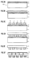
本発明のさらなる特徴、利点および合目的点は、以下に示す3つの実施例により図1〜3に基づき説明する。
【0064】
図1は、本発明による構成素子の実施例の概略的な断面図であり、
図2は、本発明による製造方法の実施例を説明した概略図であり、
図3は、本発明による導電性の緩衝層のための製造方法を説明した概略図である。
【0065】
種々異なる実施例において、同様のまたは同様に作用する構成部分には、それぞれ同じ参照符号を付与してある。
【0066】
図1に示した放射線を発する半導体チップは、薄層素子の形の半導体ボディ11を有しており、この半導体ボディ11は、導電性の緩衝層9と、特にIII−V窒化物半導体材料をベースとしたエピタキシャル層を有している層系8とからなっている。緩衝層9上には接触面12が被着されていて、この接触面12は、図1に示したものとは異なって半導体ボディ11の上側の一部しか覆っていなくてもよい。また、接触面12は、たとえばAlを有しているまたはAlからなっていて、ボンドパッドとして形成されていてよい。
【0067】
層系8の構造は、半導体ボディ11もしくはこれによって形成されるチップの機能性を規定する。この層系8は、放射線を発する役割を果たす活性層も含んでいる。
【0068】
半導体ボディ11は、エピタキシャル基板を有していない。
【0069】
半導体ボディ11は、緩衝層9の側ではn型に、これと反対の側ではp型に形成されている。
【0070】
p型の側で、半導体ボディ11は、導電性の支持体5の主面に被着されている。
【0071】
支持体5は、半導体ボディ11とは反対の側で、第2の接触面10を有している。
【0072】
有利には、このようにして形成された半導体チップは、縦方向に、つまり層面に対して垂直に一貫して導電性である。これによって、横方向に広範囲にわたって均一に電流が構成素子を通って流れることができ、かつ簡単な接触が可能となる。
【0073】
また、別の利点は、チップを側面方向に問題なくスケーリングできるということである。この場合、横方向のスケーリングとは、チップの横方向の別の設定寸法への移行と理解されたい。この移行は、チップが横方向に構造形成されていない、つまりトポロジーを有していないので、簡単にできる。
【0074】
これに対して、たとえば主面上に異なる2つの接触面を有しているような横方向に構造形成された素子では、横方向のスケーリングの際には、横方向の構造の適合を考慮しなければならない。
【0075】
縦方向に導電性のチップのための条件は、導電性の緩衝層9である。この層は、たとえば2層にIII−V窒化物半導体材料から形成されている。緩衝層9のさらに詳しい性質は、図3に基づいて導電性の緩衝層の製造と共に説明する。
【0076】
III−V窒化物半導体材料は、直接バンド遷移型でありかつバンドギャップが大きいので、本発明により形成された半導体ボディは、特に黄色、緑色、緑青色または紫色のスペクトル領域に中心波長を有する発光ダイオードチップ、特に高い光度を有する発光ダイオードおよび緑色から紫色のスペクトル領域に発光波長を有する半導体レーザーの実現のために適している。
【0077】
図2に、6つの中間段階a〜fで概略的に、本発明による製造方法の実施例を示す。
【0078】
出発点では、多層のエピタキシャル基板100が形成されている(図2a)。基板ボディ1は、SiC、有利にはポリSiCからなる。
【0079】
基板ボディ1上には、有利には、酸化ケイ素からなる固着層3が形成されていて、この固着層3は、基板ボディを、たとえばSi(111)からなる薄い成長層2に結合している。
【0080】
この場合、成長層2の厚さは、この熱膨張がこの下に設けられた基板ボディ1によってほぼ規定されるように薄く選択されている。通常、成長層2の厚さは、ほぼ0.1〜20μmであり、有利には10μmよりも小さく、特に有利には0.1〜2μmである。
【0081】
成長層2の表面には、次の段階で、III−V窒化物半導体材料からなる多数の層4を析出させる(図2)。
【0082】
この場合、有利には、まず、導電性のAlGaN緩衝層9を成長層2の表面に形成する。それというのは、GaN自体およびInGaN化合物の、Si(111)−またはSiC表面への濡れ性が悪いからである。
【0083】
緩衝層9、およびこの上に析出させるIII−V化合物半導体材料をベースとした隣接する層は、n型に形成する。
【0084】
反対の側、つまりエピタキシャル基板100と反対の側では、エピタキシャル層積層体を、1つまたは複数のp型の層によって区切る。
【0085】
n型層とp型層との間には、Al1 - x - yGaxInyN[式中、0≦x≦1、0≦x≦1、x+y≦1]ベースの多数の層を形成する。これらの層は、狭義には放射線を発する役割を果たしている。これには、当業者によく知られている放射線を発するすべての半導体構造が、特にシングル−またはダブルヘテロ構造および単一−または多重量子井戸構造を形成しているpn接合が適している。
【0086】
次の段階では、メサエッチングによって、Al1 - x - yGaxInyNベースの層を横方向に構造形成する(図2c)。これによって、エピタキシャル基板100上に互いに並んで配置された多数の個別の層積層体が形成される。これらの層積層体はほぼ、放射線を発するチップのまだ個別化されていない薄層素子11である。
【0087】
メサエッチングは、エピタキシャル基板100の成長層2内にまでおよび、これによって、次の段階で、薄層素子11をエピタキシャル基板100から簡単に剥離することができる。
【0088】
Al1 - x - yGaxInyNベースの層4の構造形成後、薄層素子11の、エピタキシャル基板100とは反対のp型の側に、支持体5または選択的には介在支持体13を被着する。支持体材料としては、たとえばGaAsまたはCuを使用することができる。
【0089】
次の段階(図2e)で、エピタキシャル基板100を薄層素子11から剥離する。この剥離は、湿式化学式にエッチングによって行い、この際、成長層2を破壊する。この場合、成長層2をエッチングによって分離する湿式化学式の剥離に必要とされるコストは、たとえばSiC基板ボディの剥離よりもはるかに小さい。
【0090】
選択的には、介在支持体13を使用して、エピタキシャル基板100を剥離した後にその位置に支持体5を被着して、その後、介在支持体13を剥離する。
【0091】
この段階の最後に形成されている構造は、両方法で極めて類似しており、相違しているのは、介在支持体13を使用する場合には、緩衝層9が、半導体ボディの、支持体5の方を向いた側に設けられているという点だけである(図2e右)。もう1つの方法では、緩衝層9が、半導体ボディ11の、支持体5とは反対の側に形成される。
【0092】
続いて、半導体ボディ11に接触面12を、支持体5に接触面10を設ける。さらに続いて、支持体5をそれぞれ半導体ボディ11間で分離し、これにより、多数の図1に示した半導体チップが得られる(図2f)。
【0093】
有利には、薄層素子11を支持体5もしくは介在支持体13への結合することによって、引き続き行うエピタキシャル基板100の剥離と関連して、エピタキシャル基板ボディ1の再使用が可能となり、これによって、SiCを基板ボディ材料として使用する場合には、大幅なコスト低減が得られる。
【0094】
さらに、SiC基板で起こるあらゆる吸収損失がなくなる。これによって、発光効率は著しく向上する。
【0095】
別の製造方法で、ポリSiCまたはポリGaNのような低コストの基板ボディを使用する場合には、その再使用に特に利点がない場合には、基板全体をエッチングで分離することもできる。
【0096】
図3で、4つの中間段階に基づき概略的に、導電性の緩衝層9の製造を説明する。
【0097】
エピタキシャル基板100としては、上で述べた製造方法のように、たとえばSi(111)を含むエピタキシャル側の成長層2を備えたSiC−またはポリSiC基板ボディ1を使用する(図3a)。
【0098】
第1の段階では、成長層2上に、多数の量子点の形の核形成層6を析出させる(図3b)。
【0099】
このための材料としては、低いAl含有量(<50%)を有するAlGaInN、InGaNまたはGaNを使用する。量子点は、高導電性であるが、閉じた層を形成していない。したがって、成長層の表面に、互いにつながっていない多数の導電性の領域が得られる。被覆度は、材料組成に応じて1〜99%と変化させることができる。
【0100】
量子点層6上に、高いAl含有量を有するAlGaNベースの、たとえばAlxGa1 - xN[式中、x>0.5]の平坦化する充填層7を析出させる(図3c)。これによって、平坦な構造9が得られる。
【0101】
導電性の領域6は、通路状の結合を緩衝層9を通して形成しており、緩衝層9の良好な導電性を保証する。
【0102】
次の段階で、緩衝層9上に、特にIII−V化合物半導体材料をベースとしたエピタキシャル層を含む層系8を析出させる(図3c)。このIII−V化合物半導体材料が主に半導体デバイスの機能性を規定する。
【0103】
薄層素子および個別の半導体チップを製造するためのさらなる段階は、たとえば図2A〜2Cに基づき説明した相応の段階に相当する。
【0104】
上に述べた実施例に基づく本発明の説明は、むろん、発明をこれらの実施例に制限するものではない。
【0105】
特に、半導体材料は、その都度与えられる範囲内で、必要条件と構成素子のために設けられた使用領域とに適合させることができる。
【0106】
さらに、半導体ボディの活性層の内部の半導体材料の組成によって、発生する放射線のセンター波長を設定することができる。
【図面の簡単な説明】
【図1】 本発明による構成素子の実施例の概略的な断面図
【図2】 本発明による製造方法の実施例を説明した概略図
【図3】 本発明による導電性の緩衝層のための製造方法を説明した概略図[0001]
The invention relates to a method for manufacturing a semiconductor chip emitting radiation based on a III-V nitride semiconductor material according to the superordinate concept of
[0002]
A semiconductor device emitting GaN-based radiation is known, for example, from US Pat. No. 5,874,747. Such a semiconductor device has a semiconductor body having a number of layers made of GaN or a material based thereon. According to the above publication, a number of layers based on GaN are deposited on a SiC substrate.
[0003]
In this case, the III-V nitride semiconductor material includes a material derived from or similar to GaN and, for example, a ternary or quaternary mixed crystal formed thereon. In particular, materials AlN, InN, AlGaN (Al 1 - x Ga x N, 0 ≦ x ≦ 1), InGaN (In 1 - x Ga x N, 0 ≦ x ≦ 1), InAlN (In 1 - x Al x N , 0 ≦ x ≦ 1) and AlInGaN (Al 1 − x − y In x Ga y N, 0 ≦ x ≦ 1, 0 ≦ y ≦ 1) belong to this.
[0004]
Hereinafter, the name “III-V nitride semiconductor” refers to the group of materials described above. In addition, the name includes the material used to form the buffer layer when the above-mentioned material-based layers are produced by epitaxial growth.
[0005]
Furthermore, it is known from US Pat. No. 5,679,152 to produce a GaN-based semiconductor body on a suitable substrate, for example a Si substrate, by epitaxial growth, in which case the GaN layer is deposited by epitaxial growth and then in situ. Remove.
[0006]
US 5786606 also discloses a GaN-based semiconductor body with an intermediate SiC substrate formed on the original epitaxial substrate. This original substrate body is removed during manufacturing.
[0007]
The use of a semiconductor body with a SiC substrate means that the additional costs for the production of semiconductor devices are not small. This is because the SiC substrate itself is very expensive. When assembling a member of a SiC substrate with a respective semiconductor body based on a III-V nitride semiconductor material to the semiconductor device, the cost for the semiconductor device is directly linked to the cost of the SiC substrate. Therefore, it is difficult to manufacture a semiconductor device at low cost.
[0008]
Furthermore, a SiC substrate in a semiconductor chip based on a III-V nitride semiconductor can lead to a decrease in luminous efficiency. This is because SiC partially absorbs radiation emitted from III-V nitride semiconductors, thereby reducing the proportion of radiation that can be emitted.
[0009]
In the manufacturing method using Si substrates described in US Pat. No. 5,679,152, only very thin substrates can be used, and these substrates must be removed immediately after epitaxial growth. Usually, the allowable thickness of such a substrate is less than 1 μm.
[0010]
This thinness of the substrate is necessary to prevent crack formation due to the different thermal expansion coefficients between silicon and III-V nitride semiconductor based materials.
[0011]
The object of the present invention is to obtain a semiconductor chip emitting radiation based on a III-V nitride semiconductor material which is technically simple and can be manufactured inexpensively and has a high external quantum efficiency.
[0012]
Furthermore, the subject of this invention is providing the manufacturing method for said semiconductor chip.
[0013]
These problems are solved by the method according to
[0014]
According to the present invention, a semiconductor chip emitting radiation based on a III-V nitride semiconductor material is formed as a thin layer element.
[0015]
In this case, a thin layer element is mainly interpreted as a semiconductor layer system consisting of a stack of epitaxial layers based on a III-V nitride semiconductor material.
[0016]
The thin layer device consists of a number of III-V nitride semiconductor epitaxial layers, where the semiconductor body is n-type epitaxial layer on one side and p-type epitaxial layer on the opposite side. Separated by layers.
[0017]
The thin-layer element is deposited on a conductive support on the p-type side, the support having a mounting surface for the thin-layer element, preferably further thin-layer element Can be used for contact.
[0018]
A corresponding contact surface is formed on the n-type side of the thin layer element. Hereinafter, the name “contact surface” refers to this contact surface unless there is a further description.
[0019]
It is particularly advantageous that the semiconductor chip thus formed does not have a normal thickness (> 100 μm) of epitaxial substrate such as, for example, a SiC substrate, and thus for semiconductor devices. The material cost is reduced.
[0020]
Another advantage of this thin layer structure is that the semiconductor body has little or no substrate that absorbs radiation.
[0021]
Accordingly, the luminous efficiency can be increased by using a reflective support.
[0022]
In another advantageous embodiment of the invention, the epitaxial layer delimited on the n-type side in the thin-layer device is formed as a conductive buffer layer.
[0023]
The formation of this buffer layer in the manufacture of GaN-based semiconductor bodies is commonly done to compensate for lattice mismatch between the epitaxial substrate and the epitaxial layer that follows the buffer layer.
[0024]
The conductive buffer layer has the great advantage that a semiconductor device that is conductive in the vertical direction can be obtained by the semiconductor body formed in this way.
[0025]
This conductive buffer layer is advantageous over an insulating buffer layer, because a vertically conductive semiconductor chip allows contact at a lower cost. Furthermore, the active layer can be expanded more in the lateral direction.
[0026]
In a particularly advantageous embodiment of the invention, the buffer layer is formed in multiple layers. The continuum of multiple layers having different compositions advantageously allows optimization of the conductivity of the buffer layer and the matching with the GaN-based layer that follows the buffer layer.
[0027]
In a preferred embodiment of the present invention, the buffer layer, AlGaN-based material such as Al 1 - [wherein, 0 ≦ x <1] x Ga x N and Al 1 - x - y In x Ga y N [ wherein , 0 ≦ x <1, 0 ≦ y <1, x + y <1].
[0028]
In this case, in particular, in order to obtain a buffer layer with good conductivity, the side of the buffer layer facing the contact surface is formed with a low Al content.
[0029]
Since the surface quality and crystal quality of the layer having such a low Al content are low, it is further advantageous to form the buffer layer on the side opposite to the contact surface with a high Al content. This high Al content increases the surface quality of the buffer layer and provides good matching to subsequent III-V nitride semiconductor based layers.
[0030]
The buffer layer has a low Al content on the side of the contact surface and a high Al content on the opposite side, so that a conductive buffer layer with a high surface quality is obtained at the same time. It is advantageous.
[0031]
According to the invention, a layer of III-V nitride semiconductor base is deposited on an epitaxial substrate for the production of a semiconductor device emitting radiation based on a III-V nitride semiconductor material. In this case, the substrate body of the epitaxial substrate has a thermal expansion coefficient compatible with the III-V nitride semiconductor material or a larger thermal expansion coefficient compared to the III-V nitride semiconductor material, and the epitaxial substrate. Are delimited on the epitaxial side by a thin growth layer, preferably comprising Si (111).
[0032]
Thus, advantageously, when manufacturing a III-V nitride semiconductor body, the thermal expansion of the epitaxial substrate is determined by the substrate body, so that the substrate behaves thermally similar to the layer to be deposited. Have
[0033]
Since the Si (111) surface has a hexagonal crystal structure, it is suitable as an epitaxial surface for III-V nitride semiconductors.
[0034]
Furthermore, the Si (111) surface can be easily processed to prepare for epitaxial growth. Si (111) processing technology is very well known and proven in the semiconductor industry because of the very common use of this material.
[0035]
Thus, it is advantageously possible to produce epitaxial substrates having a diameter that is significantly larger than the diameter of commercially available SiC substrates.
[0036]
The achievable surface quality of the Si (111) surface is also significantly improved over the surface quality of the SiC substrate.
[0037]
As the substrate body, it is advantageous to use polycrystalline SiC (poly SiC), GaN or polycrystalline GaN (poly GaN), since they are well thermally compatible with GaN-based layers. Furthermore, the substrate body may contain sapphire (α-Al 2 O 3 ). Sapphire has a larger coefficient of thermal expansion than the III-V nitride semiconductor material.
[0038]
This substrate body is significantly less expensive than the substrate used in the prior art. This is because, since the semiconductor body is deposited on the surface of the growth layer, advantageously the requirements for the crystal properties of the substrate body are reduced. This reduced demand makes it possible to use particularly low-cost polycrystalline materials.
[0039]
Advantageously, the substrate body is bonded to the growth layer by a pinned layer, which pinned layer consists of silicon oxide or silicon nitride.
[0040]
The formation of a pinned layer between the substrate body and the growth layer can be easily performed, in which case the materials mentioned above ensure a particularly stable bond.
[0041]
In a particularly advantageous embodiment of the production method according to the invention, a support is coated on the III-V nitride semiconductor-based layer in the next step following the deposition of the III-V nitride semiconductor-based layer. To wear.
[0042]
Thereafter, the epitaxial substrate is peeled off from the III-V nitride semiconductor base layer.
[0043]
This advantageously allows reuse or continued use of the epitaxial substrate or substrate body.
[0044]
The use of the Si (111) growth layer as the epitaxial surface is advantageous when peeling the epitaxial substrate. This is because the semiconductor body can be easily separated from the substrate body, for example by etching. In this case, the Si (111) growth layer becomes a sacrificial layer.
[0045]
Particularly advantageously, this manufacturing method allows a low-cost manufacturing of a semiconductor body using a single crystal SiC substrate body. This is because the costly SiC substrate body can be reused or continuously used.
[0046]
In an advantageous embodiment of the production method according to the invention, after peeling off the epitaxial substrate, a contact layer is deposited on the surface of the semiconductor body from which the epitaxial substrate has been peeled off.
[0047]
In an advantageous embodiment of the manufacturing method according to the invention, a number of III-V nitride semiconductor layers are structured before the epitaxial substrate is stripped.
[0048]
In this case, the structure formation is interpreted as a means for dividing the epitaxial layer into a number of individual epitaxial layer stacks arranged side by side on the epitaxial substrate at intervals. Advantageously, when the epitaxial layer stack is stripped by etching, this structure enlarges the surface exposed to the etching attack.
[0049]
In an advantageous embodiment of the invention, instead of the support, an intervening support is first deposited on an epitaxial layer based on a III-V nitride semiconductor material in the above-described manufacturing method. Thereafter, the epitaxial substrate is similarly peeled off, and a support is deposited on the side of the epitaxial layer from which the epitaxial substrate has been peeled off. In the next step, the intervening support is peeled off.
[0050]
According to this embodiment, the layering sequence of the layers based on the III-V nitride semiconductor material is advantageously reversed with respect to the support described above with respect to the support. Such reversal is advantageous, and it also allows use in subsequent methods, particularly packaging that requires this reversed stacking sequence.
[0051]
In a particularly advantageous embodiment of the production method according to the invention, a conductive buffer layer is deposited on the epitaxial substrate as the first layer.
[0052]
Such a buffer layer is particularly advantageous for obtaining a surface with an optimally matched lattice structure for the subsequent epitaxial layer, which at the same time is well wetted by subsequent layer materials, This allows for a uniform growth of subsequent layers.
[0053]
Since the buffer layer has conductivity, it is possible to obtain a vertically conductive semiconductor element having a positive property as described above.
[0054]
Advantageously, the buffer layer is formed from a number of individual layers based on AlGaN.
[0055]
This is advantageous because a buffer layer with a high Al content forms a surface that is lattice matched and well wettable to the next layer based on III-V nitride semiconductor material. . However, the conductivity of the buffer layer having a high Al content is low. On the other hand, a buffer layer having a low Al content conducts electricity well, but the crystal quality and surface quality are low.
[0056]
By forming such a large number of layers in combination, it is possible to combine high conductivity and high crystal quality.
[0057]
Furthermore, a layer having a relatively high Al content is formed on the substrate side, and a layer having a relatively low Al content is deposited on the epitaxial layer side, that is, on the opposite side of the buffer layer from the epitaxial substrate. And is advantageous.
[0058]
In another particularly advantageous embodiment of the production method according to the invention, the buffer layer is formed in two stages.
[0059]
In the first stage, a number of conductive regions are deposited on the growth layer of the epitaxial substrate. As the material for the conductive region, in particular, In 1 - x Ga x N [ wherein, 0 ≦ x <1] and In 1 - x - y Al x Ga y N [ wherein, 0 ≦ x InGaN based materials such as <1, 0 ≦ y <1, x + y <1] or GaN are suitable.
[0060]
In this case, since Si and Ga tend to form domains, a uniform arrangement over a wide range of conductive regions is obtained.
[0061]
In the second stage, these multiple conductive areas are covered with a filling layer to be planarized to fill the gaps between the conductive areas.
[0062]
In this case, an AlGaN compound having a high Al content is particularly suitable as the material. The buffer layer produced in this way is very well suited for the deposition of the following layers based on III-V nitride semiconductor materials and has a high electrical conductivity.
[0063]
Further features, advantages and objectives of the present invention will be described with reference to FIGS.
[0064]
FIG. 1 is a schematic cross-sectional view of an embodiment of a component according to the invention,
FIG. 2 is a schematic diagram illustrating an embodiment of a manufacturing method according to the present invention.
FIG. 3 is a schematic view illustrating a manufacturing method for a conductive buffer layer according to the present invention.
[0065]
In different embodiments, similar or similarly functioning components are each given the same reference numeral.
[0066]
The semiconductor chip emitting radiation shown in FIG. 1 has a
[0067]
The structure of the
[0068]
The
[0069]
The
[0070]
On the p-type side, the
[0071]
The
[0072]
Advantageously, the semiconductor chip thus formed is consistently conductive in the longitudinal direction, ie perpendicular to the layer plane. This allows current to flow uniformly through the component over a wide range in the lateral direction and allows simple contact.
[0073]
Another advantage is that the chip can be scaled sideways without problems. In this case, lateral scaling should be understood as a transition to another set dimension in the lateral direction of the chip. This transition can be simplified because the chip is not laterally structured, i.e. has no topology.
[0074]
On the other hand, in the case of a laterally structured element having, for example, two different contact surfaces on the main surface, the lateral structural adaptation is taken into account when scaling in the lateral direction. There must be.
[0075]
The condition for the vertically conductive chip is the
[0076]
Since III-V nitride semiconductor material is a direct band transition type and has a large band gap, the semiconductor body formed according to the present invention emits light having a central wavelength particularly in the yellow, green, green blue or violet spectral region. It is suitable for the realization of diode chips, in particular light-emitting diodes with high luminous intensity and semiconductor lasers with emission wavelengths in the green to violet spectral region.
[0077]
FIG. 2 shows an embodiment of the production method according to the invention, schematically in six intermediate stages af.
[0078]
At the starting point, a
[0079]
An
[0080]
In this case, the thickness of the
[0081]
A large number of layers 4 made of III-V nitride semiconductor material are deposited on the surface of the
[0082]
In this case, advantageously, first, a conductive
[0083]
The
[0084]
On the opposite side, that is, the side opposite the
[0085]
Between the n-type layer and the p-type layer, a number of layers based on Al 1 − x − y Ga x In y N [where 0 ≦ x ≦ 1, 0 ≦ x ≦ 1, x + y ≦ 1] are provided. Form. These layers play a role of emitting radiation in a narrow sense. For this, all semiconductor structures emitting radiation well known to those skilled in the art are suitable, in particular pn junctions forming single- or double heterostructures and single- or multiple quantum well structures.
[0086]
In the next step, the mesa etching, Al 1 - x - y Ga x In y N structures form the base layer in the transverse direction (Fig. 2c). As a result, a large number of individual layer stacks arranged side by side on the
[0087]
The mesa etching extends into the
[0088]
Al 1 - x - y Ga x In y N base after structure formation layer 4, the
[0089]
In the next stage (FIG. 2 e), the
[0090]
Optionally, using the intervening support 13, the
[0091]
The structure formed at the end of this stage is very similar in both methods, the difference being that when the intervening support 13 is used, the
[0092]
Subsequently, the
[0093]
Advantageously, the
[0094]
Furthermore, any absorption loss that occurs in the SiC substrate is eliminated. Thereby, the luminous efficiency is remarkably improved.
[0095]
In another manufacturing method, when a low-cost substrate body such as poly SiC or poly GaN is used, the entire substrate can be separated by etching if there is no particular advantage in its reuse.
[0096]
In FIG. 3, the production of the
[0097]
As the
[0098]
In the first stage, a nucleation layer 6 in the form of a number of quantum dots is deposited on the growth layer 2 (FIG. 3b).
[0099]
As a material for this, AlGaInN, InGaN or GaN having a low Al content (<50%) is used. The quantum dots are highly conductive but do not form a closed layer. Therefore, a large number of conductive regions that are not connected to each other are obtained on the surface of the growth layer. The degree of coverage can be varied from 1 to 99% depending on the material composition.
[0100]
On the quantum dot layer 6, an AlGaN-based with a high Al content, for example, Al x Ga 1 - [wherein, x> 0.5] x N precipitating
[0101]
The conductive region 6 forms a path-like bond through the
[0102]
In the next stage, a
[0103]
Further steps for manufacturing the thin-layer elements and the individual semiconductor chips correspond to the corresponding steps described, for example, with reference to FIGS.
[0104]
The description of the invention based on the embodiments described above is, of course, not limiting the invention to these embodiments.
[0105]
In particular, the semiconductor material can be adapted to the requirements and the area of use provided for the component within the range given each time.
[0106]
Furthermore, the center wavelength of the generated radiation can be set by the composition of the semiconductor material inside the active layer of the semiconductor body.
[Brief description of the drawings]
1 is a schematic cross-sectional view of an embodiment of a component according to the invention. FIG. 2 is a schematic diagram illustrating an embodiment of a manufacturing method according to the invention. FIG. 3 is for a conductive buffer layer according to the invention. Schematic explaining the manufacturing method
Claims (15)
薄層素子を支持体(5)に結合させ、
エピタキシャル基板(100)を薄層素子から除去する、III−V窒化物半導体材料をベースとした薄層素子(11)を有する放射線を発する半導体チップを製造する方法において、
エピタキシャル基板(100)が、固着層(3)によって、成長層(2)に結合されているポリSiC、ポリGaN、SiC、GaNまたはサファイアからなる基板ボディ(1)を有しており、前記成長層(2)はSi(111)層を有し、かつ前記固着層(3)は酸化ケイ素または窒化ケイ素からなり、
成長層(2)上に、薄層素子(11)の層系をエピタキシャル成長によって析出させることを特徴とする、III−V窒化物半導体材料をベースとした薄層素子(11)を有する放射線を発する半導体チップを製造する方法。Depositing the layer system of the thin layer element (11) on the epitaxial substrate (100);
The thin layer element is bonded to the support (5),
In a method for manufacturing a semiconductor chip emitting radiation having a thin layer element (11) based on a III-V nitride semiconductor material, removing the epitaxial substrate (100) from the thin layer element,
An epitaxial substrate (100) has a substrate body (1) made of poly-SiC, poly-GaN, SiC, GaN or sapphire bonded to a growth layer (2) by a pinned layer (3) , said growth Layer (2) has a Si (111) layer, and said anchoring layer (3) consists of silicon oxide or silicon nitride,
Radiation is emitted having a thin layer element (11) based on a III-V nitride semiconductor material, characterized in that a layer system of the thin layer element (11) is deposited on the growth layer (2) by epitaxial growth. A method of manufacturing a semiconductor chip.
介在支持体を層系上に被着する段階、
エピタキシャル基板を剥離する段階、
支持体(5)を、層系の、エピタキシャル基板を剥離した側に被着する段階、および
介在支持体を剥離する段階で方法を続行する、請求項1から3までのいずれか1項記載の方法。After depositing the layer system
Depositing an intervening support on the layer system;
Peeling the epitaxial substrate;
The method according to any one of claims 1 to 3 , wherein the method is continued in the step of depositing the support (5) on the side of the layer system on which the epitaxial substrate has been peeled off and in the step of peeling off the intervening support. Method.
平坦化する充填層(7)を被着する段階によって緩衝層を形成する、請求項7から10までのいずれか1項記載の方法。The number of conductive regions spaced apart from one another, forming a buffer layer by the step of depositing step, and the filling layer for flattening (7) depositing on a growth layer (2), from the claims 7 11. The method according to any one of up to 10 .
Applications Claiming Priority (2)
| Application Number | Priority Date | Filing Date | Title |
|---|---|---|---|
| DE10042947A DE10042947A1 (en) | 2000-08-31 | 2000-08-31 | Radiation-emitting semiconductor component based on GaN |
| PCT/DE2001/003348 WO2002019439A1 (en) | 2000-08-31 | 2001-08-31 | Method for producing a radiation-emitting semiconductor chip based on iii-v nitride semiconductor material, and a corresponding radiation-emitting semiconductor chip |
Related Child Applications (1)
| Application Number | Title | Priority Date | Filing Date |
|---|---|---|---|
| JP2007072671A Division JP5183085B2 (en) | 2000-08-31 | 2007-03-20 | Semiconductor chip that emits radiation |
Publications (3)
| Publication Number | Publication Date |
|---|---|
| JP2004508720A JP2004508720A (en) | 2004-03-18 |
| JP2004508720A5 JP2004508720A5 (en) | 2005-03-03 |
| JP4177097B2 true JP4177097B2 (en) | 2008-11-05 |
Family
ID=7654526
Family Applications (2)
| Application Number | Title | Priority Date | Filing Date |
|---|---|---|---|
| JP2002524235A Expired - Lifetime JP4177097B2 (en) | 2000-08-31 | 2001-08-31 | Method of manufacturing a semiconductor chip emitting radiation based on III-V nitride semiconductor and semiconductor chip emitting radiation |
| JP2007072671A Expired - Lifetime JP5183085B2 (en) | 2000-08-31 | 2007-03-20 | Semiconductor chip that emits radiation |
Family Applications After (1)
| Application Number | Title | Priority Date | Filing Date |
|---|---|---|---|
| JP2007072671A Expired - Lifetime JP5183085B2 (en) | 2000-08-31 | 2007-03-20 | Semiconductor chip that emits radiation |
Country Status (7)
| Country | Link |
|---|---|
| US (2) | US6849878B2 (en) |
| EP (1) | EP1314209B1 (en) |
| JP (2) | JP4177097B2 (en) |
| CN (1) | CN1471735B (en) |
| DE (1) | DE10042947A1 (en) |
| TW (1) | TW584971B (en) |
| WO (1) | WO2002019439A1 (en) |
Cited By (1)
| Publication number | Priority date | Publication date | Assignee | Title |
|---|---|---|---|---|
| RU2700709C1 (en) * | 2018-02-12 | 2019-09-19 | Открытое Акционерное Общество "Пеленг" | Method of determining deviations of real meteorological conditions from tabular values taken into account in calculating installations for artillery firing |
Families Citing this family (64)
| Publication number | Priority date | Publication date | Assignee | Title |
|---|---|---|---|---|
| US7319247B2 (en) * | 2000-04-26 | 2008-01-15 | Osram Gmbh | Light emitting-diode chip and a method for producing same |
| DE10051465A1 (en) | 2000-10-17 | 2002-05-02 | Osram Opto Semiconductors Gmbh | Method for producing a GaN-based semiconductor component |
| EP1277240B1 (en) * | 2000-04-26 | 2015-05-20 | OSRAM Opto Semiconductors GmbH | Method of manufacturing a light-emitting semiconductor element |
| TWI289944B (en) * | 2000-05-26 | 2007-11-11 | Osram Opto Semiconductors Gmbh | Light-emitting-diode-element with a light-emitting-diode-chip |
| JP4250909B2 (en) * | 2002-05-20 | 2009-04-08 | ソニー株式会社 | Semiconductor element separation method and transfer method |
| GB2388957A (en) * | 2002-05-24 | 2003-11-26 | Imp College Innovations Ltd | Quantum dots for extended wavelength operation |
| US6841802B2 (en) | 2002-06-26 | 2005-01-11 | Oriol, Inc. | Thin film light emitting diode |
| DE10245631B4 (en) * | 2002-09-30 | 2022-01-20 | OSRAM Opto Semiconductors Gesellschaft mit beschränkter Haftung | semiconductor device |
| DE10350707B4 (en) * | 2003-02-26 | 2014-02-13 | Osram Opto Semiconductors Gmbh | Electrical contact for optoelectronic semiconductor chip and method for its production |
| TWI243488B (en) | 2003-02-26 | 2005-11-11 | Osram Opto Semiconductors Gmbh | Electrical contact-area for optoelectronic semiconductor-chip and its production method |
| WO2004100279A2 (en) * | 2003-04-30 | 2004-11-18 | Cree, Inc. | High-power solid state light emitter package |
| US7589003B2 (en) * | 2003-06-13 | 2009-09-15 | Arizona Board Of Regents, Acting For And On Behalf Of Arizona State University, A Corporate Body Organized Under Arizona Law | GeSn alloys and ordered phases with direct tunable bandgaps grown directly on silicon |
| WO2004114368A2 (en) * | 2003-06-13 | 2004-12-29 | Arizona Board Of Regents, A Body Corporate Of The State Of Arizona Acting For And On Behalf Of Arizona State University | METHOD FOR PREPARING GE1-x-ySnxEy (E=P, As, Sb) SEMICONDUCTORS AND RELATED Si-Ge-Sn-E AND Si-Ge-E ANALOGS |
| JP4218597B2 (en) | 2003-08-08 | 2009-02-04 | 住友電気工業株式会社 | Manufacturing method of semiconductor light emitting device |
| JP4110222B2 (en) * | 2003-08-20 | 2008-07-02 | 住友電気工業株式会社 | Light emitting diode |
| EP1569263B1 (en) | 2004-02-27 | 2011-11-23 | OSRAM Opto Semiconductors GmbH | Method for joining two wafers |
| US7332365B2 (en) * | 2004-05-18 | 2008-02-19 | Cree, Inc. | Method for fabricating group-III nitride devices and devices fabricated using method |
| US7791061B2 (en) * | 2004-05-18 | 2010-09-07 | Cree, Inc. | External extraction light emitting diode based upon crystallographic faceted surfaces |
| US7534633B2 (en) * | 2004-07-02 | 2009-05-19 | Cree, Inc. | LED with substrate modifications for enhanced light extraction and method of making same |
| US7259402B2 (en) * | 2004-09-22 | 2007-08-21 | Cree, Inc. | High efficiency group III nitride-silicon carbide light emitting diode |
| US8174037B2 (en) | 2004-09-22 | 2012-05-08 | Cree, Inc. | High efficiency group III nitride LED with lenticular surface |
| US8513686B2 (en) * | 2004-09-22 | 2013-08-20 | Cree, Inc. | High output small area group III nitride LEDs |
| US7737459B2 (en) * | 2004-09-22 | 2010-06-15 | Cree, Inc. | High output group III nitride light emitting diodes |
| US8288942B2 (en) | 2004-12-28 | 2012-10-16 | Cree, Inc. | High efficacy white LED |
| US7932111B2 (en) | 2005-02-23 | 2011-04-26 | Cree, Inc. | Substrate removal process for high light extraction LEDs |
| KR100631980B1 (en) * | 2005-04-06 | 2006-10-11 | 삼성전기주식회사 | Nitride semiconductor device |
| US8575651B2 (en) * | 2005-04-11 | 2013-11-05 | Cree, Inc. | Devices having thick semi-insulating epitaxial gallium nitride layer |
| US8674375B2 (en) * | 2005-07-21 | 2014-03-18 | Cree, Inc. | Roughened high refractive index layer/LED for high light extraction |
| CN1988109B (en) * | 2005-12-21 | 2012-03-21 | 弗赖贝格化合物原料有限公司 | Process for producing a free-standing III-N layer, and free-standing III-N substrate |
| US20070194342A1 (en) * | 2006-01-12 | 2007-08-23 | Kinzer Daniel M | GaN SEMICONDUCTOR DEVICE AND PROCESS EMPLOYING GaN ON THIN SAPHIRE LAYER ON POLYCRYSTALLINE SILICON CARBIDE |
| JP2009538536A (en) | 2006-05-26 | 2009-11-05 | クリー エル イー ディー ライティング ソリューションズ インコーポレイテッド | Solid state light emitting device and method of manufacturing the same |
| EP2029936B1 (en) | 2006-05-31 | 2015-07-29 | Cree, Inc. | Lighting device and method of lighting |
| TW200802941A (en) * | 2006-06-22 | 2008-01-01 | Univ Nat Central | A quantum photoelectric element of antimony compound |
| DE102006060410A1 (en) * | 2006-06-30 | 2008-01-03 | Osram Opto Semiconductors Gmbh | Edge-emitting semiconductor laser chip |
| US7885306B2 (en) | 2006-06-30 | 2011-02-08 | Osram Opto Semiconductors Gmbh | Edge-emitting semiconductor laser chip |
| US8310143B2 (en) * | 2006-08-23 | 2012-11-13 | Cree, Inc. | Lighting device and lighting method |
| US8008694B2 (en) * | 2006-09-23 | 2011-08-30 | Ylx, Ltd. | Brightness enhancement method and apparatus of light emitting diodes |
| EP2095018A1 (en) * | 2006-12-04 | 2009-09-02 | Cree Led Lighting Solutions, Inc. | Lighting device and lighting method |
| US9310026B2 (en) | 2006-12-04 | 2016-04-12 | Cree, Inc. | Lighting assembly and lighting method |
| US8026517B2 (en) * | 2007-05-10 | 2011-09-27 | Industrial Technology Research Institute | Semiconductor structures |
| US20080303033A1 (en) * | 2007-06-05 | 2008-12-11 | Cree, Inc. | Formation of nitride-based optoelectronic and electronic device structures on lattice-matched substrates |
| JP5431320B2 (en) * | 2007-07-17 | 2014-03-05 | クリー インコーポレイテッド | Optical element having internal optical function and method for manufacturing the same |
| KR100872678B1 (en) * | 2007-07-23 | 2008-12-10 | 엘지이노텍 주식회사 | Manufacturing method of semiconductor light emitting device |
| JP4148367B1 (en) | 2007-08-02 | 2008-09-10 | 富山県 | Cell screening method |
| US8617997B2 (en) | 2007-08-21 | 2013-12-31 | Cree, Inc. | Selective wet etching of gold-tin based solder |
| US11114594B2 (en) | 2007-08-24 | 2021-09-07 | Creeled, Inc. | Light emitting device packages using light scattering particles of different size |
| JP5212777B2 (en) * | 2007-11-28 | 2013-06-19 | スタンレー電気株式会社 | Semiconductor light emitting device and lighting device |
| US8021487B2 (en) * | 2007-12-12 | 2011-09-20 | Veeco Instruments Inc. | Wafer carrier with hub |
| US20110114022A1 (en) * | 2007-12-12 | 2011-05-19 | Veeco Instruments Inc. | Wafer carrier with hub |
| US9431589B2 (en) | 2007-12-14 | 2016-08-30 | Cree, Inc. | Textured encapsulant surface in LED packages |
| US9012253B2 (en) * | 2009-12-16 | 2015-04-21 | Micron Technology, Inc. | Gallium nitride wafer substrate for solid state lighting devices, and associated systems and methods |
| DE102009060749B4 (en) * | 2009-12-30 | 2021-12-30 | OSRAM Opto Semiconductors Gesellschaft mit beschränkter Haftung | Optoelectronic semiconductor chip |
| US8329482B2 (en) | 2010-04-30 | 2012-12-11 | Cree, Inc. | White-emitting LED chips and method for making same |
| US8997832B1 (en) | 2010-11-23 | 2015-04-07 | Western Digital (Fremont), Llc | Method of fabricating micrometer scale components |
| US20130330911A1 (en) * | 2012-06-08 | 2013-12-12 | Yi-Chiau Huang | Method of semiconductor film stabilization |
| US9064709B2 (en) * | 2012-09-28 | 2015-06-23 | Intel Corporation | High breakdown voltage III-N depletion mode MOS capacitors |
| US10134727B2 (en) | 2012-09-28 | 2018-11-20 | Intel Corporation | High breakdown voltage III-N depletion mode MOS capacitors |
| US9911813B2 (en) * | 2012-12-11 | 2018-03-06 | Massachusetts Institute Of Technology | Reducing leakage current in semiconductor devices |
| US8896008B2 (en) | 2013-04-23 | 2014-11-25 | Cree, Inc. | Light emitting diodes having group III nitride surface features defined by a mask and crystal planes |
| DE102014116141B4 (en) | 2014-11-05 | 2022-07-28 | OSRAM Opto Semiconductors Gesellschaft mit beschränkter Haftung | Method for producing at least one optoelectronic semiconductor chip, optoelectronic semiconductor chip and optoelectronic semiconductor component |
| DE102017108385A1 (en) | 2017-04-20 | 2018-10-25 | Osram Opto Semiconductors Gmbh | Laser bars and semi-conductor lasers and methods for producing laser bars and semiconductor lasers |
| TWI637481B (en) * | 2017-11-29 | 2018-10-01 | 財團法人工業技術研究院 | Semiconductor structure, light-emitting device and manufacturing method for the same |
| DE102018104785A1 (en) * | 2018-03-02 | 2019-09-05 | Osram Opto Semiconductors Gmbh | Method for producing a plurality of transferable components and component assembly of components |
| DE102018104778A1 (en) * | 2018-03-02 | 2019-09-05 | Osram Opto Semiconductors Gmbh | Component assembly of optical components, method for producing a composite component and component with an optical component |
Family Cites Families (45)
| Publication number | Priority date | Publication date | Assignee | Title |
|---|---|---|---|---|
| JPH0760790B2 (en) * | 1987-05-13 | 1995-06-28 | シャープ株式会社 | Compound semiconductor substrate |
| US4912532A (en) * | 1988-08-26 | 1990-03-27 | Hewlett-Packard Company | Electro-optical device with inverted transparent substrate and method for making same |
| JP2542447B2 (en) * | 1990-04-13 | 1996-10-09 | 三菱電機株式会社 | Solar cell and method of manufacturing the same |
| US5244818A (en) * | 1992-04-08 | 1993-09-14 | Georgia Tech Research Corporation | Processes for lift-off of thin film materials and for the fabrication of three dimensional integrated circuits |
| US5286335A (en) * | 1992-04-08 | 1994-02-15 | Georgia Tech Research Corporation | Processes for lift-off and deposition of thin film materials |
| US5391257A (en) * | 1993-12-10 | 1995-02-21 | Rockwell International Corporation | Method of transferring a thin film to an alternate substrate |
| US5679152A (en) | 1994-01-27 | 1997-10-21 | Advanced Technology Materials, Inc. | Method of making a single crystals Ga*N article |
| JP2669368B2 (en) * | 1994-03-16 | 1997-10-27 | 日本電気株式会社 | Method for manufacturing compound semiconductor laminated structure on Si substrate |
| US5585648A (en) * | 1995-02-03 | 1996-12-17 | Tischler; Michael A. | High brightness electroluminescent device, emitting in the green to ultraviolet spectrum, and method of making the same |
| US5670798A (en) * | 1995-03-29 | 1997-09-23 | North Carolina State University | Integrated heterostructures of Group III-V nitride semiconductor materials including epitaxial ohmic contact non-nitride buffer layer and methods of fabricating same |
| US5739554A (en) * | 1995-05-08 | 1998-04-14 | Cree Research, Inc. | Double heterojunction light emitting diode with gallium nitride active layer |
| US5798537A (en) * | 1995-08-31 | 1998-08-25 | Kabushiki Kaisha Toshiba | Blue light-emitting device |
| JP3182346B2 (en) * | 1995-08-31 | 2001-07-03 | 株式会社東芝 | Blue light emitting device and method of manufacturing the same |
| JP3409958B2 (en) * | 1995-12-15 | 2003-05-26 | 株式会社東芝 | Semiconductor light emitting device |
| US5874747A (en) * | 1996-02-05 | 1999-02-23 | Advanced Technology Materials, Inc. | High brightness electroluminescent device emitting in the green to ultraviolet spectrum and method of making the same |
| US5985687A (en) | 1996-04-12 | 1999-11-16 | The Regents Of The University Of California | Method for making cleaved facets for lasers fabricated with gallium nitride and other noncubic materials |
| JPH1022226A (en) * | 1996-07-05 | 1998-01-23 | Super Silicon Kenkyusho:Kk | Method and device for producing epitaxial wafer |
| US5684309A (en) * | 1996-07-11 | 1997-11-04 | North Carolina State University | Stacked quantum well aluminum indium gallium nitride light emitting diodes |
| JP3214367B2 (en) | 1996-08-12 | 2001-10-02 | 豊田合成株式会社 | Method for manufacturing semiconductor light emitting device |
| JPH10215035A (en) | 1997-01-30 | 1998-08-11 | Toshiba Corp | Compound semiconductor element and manufacture thereof |
| US5880491A (en) * | 1997-01-31 | 1999-03-09 | The United States Of America As Represented By The Secretary Of The Air Force | SiC/111-V-nitride heterostructures on SiC/SiO2 /Si for optoelectronic devices |
| JP3914615B2 (en) | 1997-08-19 | 2007-05-16 | 住友電気工業株式会社 | Semiconductor light emitting device and manufacturing method thereof |
| US6033995A (en) * | 1997-09-16 | 2000-03-07 | Trw Inc. | Inverted layer epitaxial liftoff process |
| US6201262B1 (en) * | 1997-10-07 | 2001-03-13 | Cree, Inc. | Group III nitride photonic devices on silicon carbide substrates with conductive buffer interlay structure |
| JP3036495B2 (en) * | 1997-11-07 | 2000-04-24 | 豊田合成株式会社 | Method for manufacturing gallium nitride-based compound semiconductor |
| JPH11145515A (en) * | 1997-11-10 | 1999-05-28 | Mitsubishi Cable Ind Ltd | Gan semiconductor light-emitting element and manufacture thereof |
| US6599133B2 (en) * | 1997-11-18 | 2003-07-29 | Technologies And Devices International, Inc. | Method for growing III-V compound semiconductor structures with an integral non-continuous quantum dot layer utilizing HVPE techniques |
| JPH11284228A (en) * | 1998-03-30 | 1999-10-15 | Toyoda Gosei Co Ltd | Semiconductor element |
| JP4126749B2 (en) * | 1998-04-22 | 2008-07-30 | ソニー株式会社 | Manufacturing method of semiconductor device |
| JP3525061B2 (en) * | 1998-09-25 | 2004-05-10 | 株式会社東芝 | Method for manufacturing semiconductor light emitting device |
| US6329063B2 (en) * | 1998-12-11 | 2001-12-11 | Nova Crystals, Inc. | Method for producing high quality heteroepitaxial growth using stress engineering and innovative substrates |
| US6744800B1 (en) * | 1998-12-30 | 2004-06-01 | Xerox Corporation | Method and structure for nitride based laser diode arrays on an insulating substrate |
| JP2000208822A (en) * | 1999-01-11 | 2000-07-28 | Matsushita Electronics Industry Corp | Semiconductor light-emitting device |
| US6328796B1 (en) * | 1999-02-01 | 2001-12-11 | The United States Of America As Represented By The Secretary Of The Navy | Single-crystal material on non-single-crystalline substrate |
| US20010042866A1 (en) * | 1999-02-05 | 2001-11-22 | Carrie Carter Coman | Inxalygazn optical emitters fabricated via substrate removal |
| WO2001006546A2 (en) * | 1999-07-16 | 2001-01-25 | Massachusetts Institute Of Technology | Silicon on iii-v semiconductor bonding for monolithic optoelectronic integration |
| US6214733B1 (en) * | 1999-11-17 | 2001-04-10 | Elo Technologies, Inc. | Process for lift off and handling of thin film materials |
| US6646292B2 (en) * | 1999-12-22 | 2003-11-11 | Lumileds Lighting, U.S., Llc | Semiconductor light emitting device and method |
| US6495867B1 (en) * | 2000-07-26 | 2002-12-17 | Axt, Inc. | InGaN/AlGaN/GaN multilayer buffer for growth of GaN on sapphire |
| US6562648B1 (en) * | 2000-08-23 | 2003-05-13 | Xerox Corporation | Structure and method for separation and transfer of semiconductor thin films onto dissimilar substrate materials |
| US6583034B2 (en) * | 2000-11-22 | 2003-06-24 | Motorola, Inc. | Semiconductor structure including a compliant substrate having a graded monocrystalline layer and methods for fabricating the structure and semiconductor devices including the structure |
| US6498073B2 (en) * | 2001-01-02 | 2002-12-24 | Honeywell International Inc. | Back illuminated imager with enhanced UV to near IR sensitivity |
| US6497763B2 (en) * | 2001-01-19 | 2002-12-24 | The United States Of America As Represented By The Secretary Of The Navy | Electronic device with composite substrate |
| JP4211256B2 (en) * | 2001-12-28 | 2009-01-21 | セイコーエプソン株式会社 | Semiconductor integrated circuit, semiconductor integrated circuit manufacturing method, electro-optical device, and electronic apparatus |
| US6562127B1 (en) * | 2002-01-16 | 2003-05-13 | The United States Of America As Represented By The Secretary Of The Navy | Method of making mosaic array of thin semiconductor material of large substrates |
-
2000
- 2000-08-31 DE DE10042947A patent/DE10042947A1/en not_active Withdrawn
-
2001
- 2001-08-30 TW TW090121292A patent/TW584971B/en not_active IP Right Cessation
- 2001-08-31 EP EP01967062A patent/EP1314209B1/en not_active Expired - Lifetime
- 2001-08-31 WO PCT/DE2001/003348 patent/WO2002019439A1/en active Application Filing
- 2001-08-31 CN CN018181406A patent/CN1471735B/en not_active Expired - Lifetime
- 2001-08-31 JP JP2002524235A patent/JP4177097B2/en not_active Expired - Lifetime
-
2003
- 2003-02-28 US US10/377,363 patent/US6849878B2/en not_active Expired - Lifetime
-
2004
- 2004-12-20 US US11/017,615 patent/US7105370B2/en not_active Expired - Lifetime
-
2007
- 2007-03-20 JP JP2007072671A patent/JP5183085B2/en not_active Expired - Lifetime
Cited By (1)
| Publication number | Priority date | Publication date | Assignee | Title |
|---|---|---|---|---|
| RU2700709C1 (en) * | 2018-02-12 | 2019-09-19 | Открытое Акционерное Общество "Пеленг" | Method of determining deviations of real meteorological conditions from tabular values taken into account in calculating installations for artillery firing |
Also Published As
| Publication number | Publication date |
|---|---|
| EP1314209A1 (en) | 2003-05-28 |
| JP2004508720A (en) | 2004-03-18 |
| US6849878B2 (en) | 2005-02-01 |
| JP5183085B2 (en) | 2013-04-17 |
| EP1314209B1 (en) | 2012-10-03 |
| CN1471735B (en) | 2010-05-26 |
| JP2007201493A (en) | 2007-08-09 |
| TW584971B (en) | 2004-04-21 |
| DE10042947A1 (en) | 2002-03-21 |
| US7105370B2 (en) | 2006-09-12 |
| US20050104083A1 (en) | 2005-05-19 |
| CN1471735A (en) | 2004-01-28 |
| US20030197170A1 (en) | 2003-10-23 |
| WO2002019439A1 (en) | 2002-03-07 |
Similar Documents
| Publication | Publication Date | Title |
|---|---|---|
| JP4177097B2 (en) | Method of manufacturing a semiconductor chip emitting radiation based on III-V nitride semiconductor and semiconductor chip emitting radiation | |
| RU2515205C2 (en) | Semiconductor light-emitting devices grown on composite wafers | |
| TWI377697B (en) | Method for growing a nitride-based iii-v group compound semiconductor | |
| JP5021302B2 (en) | Manufacturing method of semiconductor chip | |
| KR101194844B1 (en) | light emitting diode device and method of manufacturing the same | |
| US20040124428A1 (en) | Light emitting diode and method of making the same | |
| US9117943B2 (en) | Semiconductor package with through silicon vias | |
| JP2004512688A (en) | Method of manufacturing a GaN-based semiconductor device | |
| KR20110030542A (en) | Method for producing an optoelectronic component and optoelectronic component | |
| US20080093611A1 (en) | Method for Production of a Radiation-Emitting Semiconductor Chip | |
| JP2010123717A (en) | Semiconductor light emitting element and method for manufacturing it | |
| JP2008047860A (en) | Method of forming rugged surface and method of manufacturing gallium nitride light-emitting diode device using the same | |
| CN101794849B (en) | Wet etching stripping method of SiC-substrate GaN-based LED | |
| WO2012090252A1 (en) | Semiconductor device and process for production thereof | |
| JP2013542608A (en) | Method for forming composite substrate | |
| US20080265272A1 (en) | Light Emitting Device Having Zener Diode Therein And Method Of Fabricating The Same | |
| KR20080061697A (en) | Vertical light emitting diode having patterned semiconductor layer by using anodic aluminum oxide and fabrication method of the same | |
| KR101072200B1 (en) | Light emitting device and method for fabricating the same | |
| KR20100109169A (en) | Fabrication method of light emitting diode and the light emitting diode fabricated by the method | |
| KR101111748B1 (en) | Method of manufacturing vertical structure nitride-gallium-based semiconductor light emitting device | |
| KR101480551B1 (en) | vertical structured group 3 nitride-based light emitting diode and its fabrication methods | |
| JP7447151B2 (en) | Light emitting diode precursor including passivation layer | |
| US20110024775A1 (en) | Methods for and devices made using multiple stage growths | |
| CN102640258B (en) | Method of manufacturing nitride semiconductor device | |
| JP3728305B2 (en) | Light emitting diode device using selective growth |
Legal Events
| Date | Code | Title | Description |
|---|---|---|---|
| A131 | Notification of reasons for refusal |
Free format text: JAPANESE INTERMEDIATE CODE: A131 Effective date: 20060510 |
|
| A521 | Request for written amendment filed |
Free format text: JAPANESE INTERMEDIATE CODE: A523 Effective date: 20060810 |
|
| A131 | Notification of reasons for refusal |
Free format text: JAPANESE INTERMEDIATE CODE: A131 Effective date: 20060922 |
|
| A601 | Written request for extension of time |
Free format text: JAPANESE INTERMEDIATE CODE: A601 Effective date: 20061219 |
|
| A602 | Written permission of extension of time |
Free format text: JAPANESE INTERMEDIATE CODE: A602 Effective date: 20061226 |
|
| A521 | Request for written amendment filed |
Free format text: JAPANESE INTERMEDIATE CODE: A523 Effective date: 20070320 |
|
| A02 | Decision of refusal |
Free format text: JAPANESE INTERMEDIATE CODE: A02 Effective date: 20070815 |
|
| A521 | Request for written amendment filed |
Free format text: JAPANESE INTERMEDIATE CODE: A523 Effective date: 20071213 |
|
| A911 | Transfer to examiner for re-examination before appeal (zenchi) |
Free format text: JAPANESE INTERMEDIATE CODE: A911 Effective date: 20071220 |
|
| TRDD | Decision of grant or rejection written | ||
| A01 | Written decision to grant a patent or to grant a registration (utility model) |
Free format text: JAPANESE INTERMEDIATE CODE: A01 Effective date: 20080723 |
|
| A01 | Written decision to grant a patent or to grant a registration (utility model) |
Free format text: JAPANESE INTERMEDIATE CODE: A01 |
|
| A61 | First payment of annual fees (during grant procedure) |
Free format text: JAPANESE INTERMEDIATE CODE: A61 Effective date: 20080821 |
|
| FPAY | Renewal fee payment (event date is renewal date of database) |
Free format text: PAYMENT UNTIL: 20110829 Year of fee payment: 3 |
|
| R150 | Certificate of patent or registration of utility model |
Ref document number: 4177097 Country of ref document: JP Free format text: JAPANESE INTERMEDIATE CODE: R150 Free format text: JAPANESE INTERMEDIATE CODE: R150 |
|
| FPAY | Renewal fee payment (event date is renewal date of database) |
Free format text: PAYMENT UNTIL: 20110829 Year of fee payment: 3 |
|
| FPAY | Renewal fee payment (event date is renewal date of database) |
Free format text: PAYMENT UNTIL: 20120829 Year of fee payment: 4 |
|
| R250 | Receipt of annual fees |
Free format text: JAPANESE INTERMEDIATE CODE: R250 |
|
| FPAY | Renewal fee payment (event date is renewal date of database) |
Free format text: PAYMENT UNTIL: 20120829 Year of fee payment: 4 |
|
| FPAY | Renewal fee payment (event date is renewal date of database) |
Free format text: PAYMENT UNTIL: 20130829 Year of fee payment: 5 |
|
| R250 | Receipt of annual fees |
Free format text: JAPANESE INTERMEDIATE CODE: R250 |
|
| R250 | Receipt of annual fees |
Free format text: JAPANESE INTERMEDIATE CODE: R250 |
|
| R250 | Receipt of annual fees |
Free format text: JAPANESE INTERMEDIATE CODE: R250 |
|
| R250 | Receipt of annual fees |
Free format text: JAPANESE INTERMEDIATE CODE: R250 |
|
| R250 | Receipt of annual fees |
Free format text: JAPANESE INTERMEDIATE CODE: R250 |
|
| R250 | Receipt of annual fees |
Free format text: JAPANESE INTERMEDIATE CODE: R250 |
|
| R250 | Receipt of annual fees |
Free format text: JAPANESE INTERMEDIATE CODE: R250 |
|
| R250 | Receipt of annual fees |
Free format text: JAPANESE INTERMEDIATE CODE: R250 |
|
| R250 | Receipt of annual fees |
Free format text: JAPANESE INTERMEDIATE CODE: R250 |
|
| R250 | Receipt of annual fees |
Free format text: JAPANESE INTERMEDIATE CODE: R250 |
|
| EXPY | Cancellation because of completion of term |