【0001】
【発明の属する技術分野】
本発明は、幅広い露光ラチチュードに対応した広いダイナミックレンジを有する固体撮像素子及び固体撮像装置、更に、上記固体撮像装置を搭載したカメラに関する。
【0002】
【従来の技術】
現在、画像を取得する通常の固体撮像装置は、シリコンプロセスの半導体微細加工技術を用いて、単結晶シリコン基板上に作成されている。
【0003】
従来の広ダイナミックレンジ(以下「DR」)を有する固体撮像装置には、例えば下記特許文献1、下記特許文献2に記載の複数枚の画像からダイナミックレンジが拡大された1枚の画像を得る方法、下記特許文献3、下記特許文献4に記載の対数圧縮センサ、下記特許文献5、下記特許文献6に記載の複数回、あるいは時間の異なる読み出しをする方法、下記特許文献7、下記特許文献8に記載の画素に複数個の感光領域を設ける方法等が有る。
【0004】
また、下記特許文献9におい、画素領域に縦方向に3つのホトダイオード(以下「PD」)を形成して、色分離、検出を行った例が知られている。
【0005】
図16は、下記特許文献9における固体撮像装置の画素領域での縦断面構造を示す図である。
【0006】
n型半導体基板上のp型不純物領域201内に、表面から異なる深さにn+型不純物領域から成る画素領域202−a,202−b,202−cが設けられている。203,204は信号を読み出すために表面に設けられたn+型不純物領域である。205は、入射光である。基板表面からの深さによって分光感度特性が異なり、深いほど長波長成分の感度が高い。画素領域202−a,202−b,202−cは、青、緑、赤に対応し、発生した信号電荷はそれぞれ独立して読み出される。
【0007】
【特許文献1】
特開昭64−89770号公報
【特許文献2】
特開平7−203320号公報
【特許文献3】
特開平1−253960号公報
【特許文献4】
特開平6−310700号公報
【特許文献5】
特開平2−50584号公報
【特許文献6】
特開平6−165026号公報
【特許文献7】
特開平7−38087号公報
【特許文献8】
特開2000−13690号公報
【特許文献9】
特開平7−74340号公報
【0008】
【発明が解決しようとする課題】
しかし前述の複数枚の画像から1枚の画像を得る方法では、複数枚のイメージセンサや撮像のタイミングを変えて複数回撮像する必要が生じる。そして前者では固体撮像装置のシステムを複雑高価にし、後者では動画に対応することが困難となる。
【0009】
また前記対数圧縮センサを用いる場合には前記画像の光電変換特性の傾き(γ)が寝てくるため、輝度再現性、色再現性と言った特性が悪化し、鑑賞に耐えない画像となりがちである。そのため前記センサは監視カメラ等の特殊用途でしか使用されることがない。
【0010】
また前記複数回の読み出しを行う方法では、同様な理由で動画に対応することができない。また静止画においてもブレが生じてしまう。
【0011】
その点、同一画素に複数個の感光領域、光電変換部を有するイメージセンサにおいては前述のようなことはなく、他の方法に比べて比較的良好な画像を取得することができる。
【0012】
しかし複数個の光電変換部が同一画素に平面方向に配置されているため、
(1)面積効率が悪い
(2)各々の光電変換部の面積が小さくなる
(3)飽和電荷量が減る
(4)各々の光電変換部の重心位置が異なるため、空間周波数特性の悪化、モアレが生じる
等の問題が残存している。
【0013】
他のセンサが画素の大部分に光電変換部であるPDを形成するのに対して、広DRセンサでは複数個のPDを平面方向に形成する必要があることから、画素面積の有効利用がより困難となっている。
【0014】
また、各々の光電変換部、PDの面積が減少することにより、前記PDに蓄積可能な電荷の最大値(飽和電荷量)も減少する。
【0015】
これは同一光量の光を当てた場合には、より早く、低い光量で前記PDが飽和することを意味し、前記DRを広げるためには例えばNDフィルタを配置する等、新たな工夫も必要となる。
【0016】
また前記飽和電荷量の低下は前記PDに蓄積される電子数Nの減少を意味し、ランダムノイズ(√N/N)が悪化する。そしてこれは画質の低下を生じさせる。
【0017】
また、画素内での各々の光電変換部、PDの位置が異なっているため、前記各々の光電変換部の出力信号から作成した感度の異なる画像同士は、画素ピッチ以下の微小な空間的なずれを有している。そのため何らかの位置補正が必要となるが、場合によってはモアレ縞を生じることが有る。
【0018】
また、画素領域に深さ方向に3つのPDを形成して、色分離、検出を行った例は、ダイナミックレンジを向上させることを目的としていないし、信号電荷を独立して読み出すものであり、複数の信号から1つの画素信号を形成していない。
【0019】
【課題を解決するための手段】
本発明の固体撮像素子は、複数の画素が配列され、前記各画素には各々異なる飽和光量を示す複数の光電変換部が半導体基板の異なる深さ方向に配置されている。
【0020】
本発明の固体撮像装置は、複数の画素が配列され、前記各画素には各々異なる飽和光量を示す複数の光電変換部が半導体基板の異なる深さ方向に配置されている固体撮像素子を用いて、前記複数の光電変換部から出力される複数の電気信号から、後段の電気回路により1つの画素信号を形成する。
【0021】
更に、本発明のカメラは、固体撮像素子又は固体撮像装置を有する。
【0022】
本発明による構成によれば、ダイナミックレンジが広く、S/N比の良好な固体撮像装置を提供することが可能となる。
【0023】
【発明の実施の形態】
以下、本発明の実施の形態について図面を用いて詳細に説明する。
【0024】
図3、図4、図5、図7、図8において、図1と共通の箇所には同一の符号が付されている。また、図12において、図10と共通の箇所には同一の符号が付されている。
【0025】
[実施形態1]
図1は、本発明の実施形態1である、固体撮像素子の1つの緑(G)画素の概略断面図である。
【0026】
前記画素は2次元アレイ状に配列している。前記画素の大きさは10μm角であり、その中に2つの光電変換部であるPDが形成されている。11は、半導体基板、例えば前記固体撮像素子が形成されている不純物濃度10−16/cm−3のp型単結晶シリコン基板であり、その表面には大きさ5μm角、深さ1μmのn+拡散層12−aと、深さ2から3μmのn+拡散層12−bが形成されている。
【0027】
前記両n+拡散層12は前記p型基板11とp−n接合を形成し、光電変換部であるPDを形成している。両者のPDの重心は、平面方向では同じ位置になるように設計されている。
【0028】
前記PDの接合容量は、12−aに相当するものが7fF、12−bのものが14fFである。
【0029】
また、前記n+拡散層12−aの電位は、図示しない表面電極によって引き出されている。また前記n+拡散層12−bは表面に設けられたn+拡散層13と電気的に接続されており、この電位も同様に図示しない表面電極によって引き出されている。
【0030】
14は入射光である撮像光であり、緑(G)のカラーフィルタ15によって波長550nm近傍の光のみが透過され、前記2つのPDに入射するようになっている。
【0031】
また、16はアルミ膜からなる、不要光を遮光する遮光膜であり、17は、バリアである。
【0032】
また、前記G画素の周囲には、赤(R)、青(B)の各画素が、前記カラーフィルタ15の組成のみを代えて配置されている。
【0033】
図2は、本実施形態における画素部分の深さ方向のポテンシャル分布図である。
【0034】
図中の12−aは前記図1のn+拡散層12−aに相当する部分であり、光蓄積開始時にはp型基板11に対して+1Vの逆バイアスが印加されている。
【0035】
同様に12−bはn+拡散層12−bに相当する部分であり、同様な+1Vの逆バイアスが印加されている。
【0036】
図1に示した2つのPDに撮像光が入射すると、前記2つのPDにおいて光電変換が行われ、その結果、光電荷である電子が前記2つのPDに蓄積する。
【0037】
図9は、本実施形態における、固体撮像素子の2つのPDから成る光電変換部の光電変換特性(出力特性)を示す図である。
【0038】
横軸は前記固体撮像素子の画素に入射する入射光量であり、縦軸は各PDの出力電圧である。また121は浅い方のPD12−aの特性であり、122は深い方のPD12−bのそれである。
【0039】
シリコン界面から近く浅い方のPD12−aにはより多くの光が当たるため、こちらの方が早く飽和レベルに達する。次いで深い方のPD12−bが飽和するため、こちらの方が広いDRを有している。但し低照度側ではシグナルレベルがノイズレベルと近いため、S/N比が悪い。
【0040】
また前記PD12から溢れ出る飽和電荷量を超えた電子は、前記p型基板11によって吸い上げられるか、あるいは存在するホールと再結合し消滅する。
【0041】
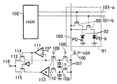
図10は、本実施形態における固体撮像装置の駆動回路図である。
【0042】
91は、1つの画素であり、その中には前述したように深さ方向に2つのPD92(PD−a,PD−b)が形成されている。
【0043】
各々のPD92は、表面から電極によって引き出され、マトリクストランジスタ99を介して垂直信号線103に接続されている。
【0044】
トランジスタ99はスイッチとして機能するMOSFETであり、水平線選択レジスタ(以下「HSR」)102により水平線101−a,101−bを介してトランジスタ99が制御される。
【0045】
前記垂直信号線103には2つのトランジスタ105,107を介して、蓄積容量108が接続されている。2つの蓄積容量108は、それぞれトランジスタ110を介してコンパレータ111とトランジスタ114、一方は乗算器113とトランジスタ115に接続されている。
【0046】
104,106,109は端子である。
【0047】
前記コンパレータ111の出力はトランジスタ114のゲートとインバータ112に入力し、インバータ112の出力はトランジスタ115のゲートに入力している。
【0048】
また、トランジスタ114,115の主電極は、画素信号出力端子116に接続されている。
【0049】
図14は、本実施形態における固体撮像装置の動作フローを示す図である。
【0050】
以下、図14を用いて、本実施形態の固体撮像装置の動作を説明する。図14に示したフローは、1画素分の画素信号を取得するための動作フローである。
【0051】
まず垂直信号線103を用いて、2つのPD92のリセットを行う。これにより、前記2つのPD92は基板に対して+1Vに逆バイアスされる。(画素リセットステップ)
次に撮像光が画素に照射されることによってシリコン基板内部で光電変換が行われ、前記PD92に光電荷の蓄積が行われる。図2で説明したように、蓄積される電荷は12−a>12−bである。(光電荷蓄積ステップ)
次に電荷を読み出す前に、信号処理系のリセットが行われる。
【0052】
トランジスタ99,110を非導通の状態で垂直信号線103を用いて、蓄積容量108やその他の寄生容量の電位をGND電位に固定する。(処理系リセットステップ)
次いでまず浅い側のPD−aの蓄積電荷を読み出す。
【0053】
一方のトランジスタ99を導通して垂直信号線103、トランジスタ105,107を介して一方の容量108に容量分割で移動、蓄積される。(PD−a読出ステップ)
次に同様にして深い側のPD−bの読み出しを行う。(PD−b読出ステップ)
各々の蓄積容量中に蓄積されたPD信号は、トランジスタ110を同時に開くことによりPD−aはコンパレータ111とトランジスタ114の主電極に、PD−bは乗算器113を通り予め決められた係数倍の掛け算が行われてトランジスタ115の主電極に印加される。前記係数とは、図9に示されたカーブ121と122のスロープ部分の傾きの比である。(乗算ステップ)
次いで前記コンパレータ111において0Vに近い値のVrefと比較され、それよりも入力電圧であるPD−a蓄積電圧が高い場合(不飽和状態)には正の電圧を、低い場合(飽和状態)には負の電圧を出力する。前記出力された電圧はインバータ112において正負反転され、トランジスタ115のゲートに入力する。(信号比較、選択ステップ)
従って前記PD−aが不飽和な場合には、前記トランジスタ114のみが導通し、前記PD−aの蓄積電圧はそのまま画素信号出力端子116に出力される。それに対して、前記PD−aが飽和した場合には、前記トランジスタ115のみが導通し、代わりに前記PD−bの蓄積電圧が前記端子116に出力される。(画素信号読出ステップ)
以上の動作が画素数分繰り返される。前記動作はHSR102や垂直線駆動回路、前述の各制御端子を駆動することで行われる。これにより各画素信号から1枚のフレーム画像を形成することができる。
【0054】
図11は、実施形態1における固体撮像装置の駆動回路の光電変換特性を示す図である。
【0055】
本実施形態によれば、前記画素から出力される画素信号は、図11に示したようなものになる。ここでIaはPD−aの飽和光量、IbはPD−bの飽和光量である。
【0056】
本実施形態によれば、高照度側では感度が低くDRが広いPDを用い、低照度側では感度が高くS/N比が良いPDを切り替えて用いることにより、幅広いレインジで良好なS/N比を確保している。このようにして得られたフレーム画像は、公知の一般画像と比べるとDRやS/N比が改善されている。
【0057】
また本実施形態の光電変換部の面積効率は5μm角/10μm角=25%と、満足できる値である。また前記2つのPDを深さ方向に重ね合わせて配置したため、それによるPD面積の減少は生じない。また前記PDを重ね合わせたことにより生じる飽和電荷量の低下も、無視できる値である。
【0058】
またPD重心の空間方向の位置も2つのそれで一致しているため、モアレの発生は生じない。
【0059】
また本実施形態に用いた画素の色配置はR,G,Bに限らず公知の任意のそれで良い。
【0060】
また前記各画素の深さ方向に形成するPDの数は2つに限ることは無く、任意の個数で良い。
【0061】
また前記各PDの形成する深さは任意であるが、少なくとも前記各色の光が前記PDに到達しないとその効果は無い。このような到達深さとは、可視光の長波長側では10μm、短波長側では1μm程度である。従って前記RやB画素においては、前記各PD深さをGのそれとは変えることもかなり有効である。
【0062】
また前記各PDからの読み出し方法は、上述のそれに限らず任意の公知のそれで良い。
【0063】
前記深い方のPDにより沢山の蓄積電荷がたまるように設計すれば、それだけDRが拡大する。
【0064】
[実施形態2]
図3は、本発明の実施形態2における、固体撮像素子の1つの緑(G)画素の概略断面図である。
【0065】
32−aは浅い方のPDを形成するn+拡散層であり、拡散深さ0.8μmで形成されている。32−bは深い方のそれであり、拡散深さ1.8μmから3.0μmで形成されている。後者は前者に比べてn+拡散層の厚さが厚く、より大きな容量を有している。そのため多くの光電荷を蓄積可能であり、より高照度の光を照射しても飽和することがない。
【0066】
33は、n+拡散層32−bと接続されているn+拡散層である。37は、バリアである。
【0067】
[実施形態3]
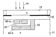
図4は、本発明の実施形態3における、固体撮像素子の1つの緑(G)画素の概略断面図である。
【0068】
42−aは浅い方のPDを形成するn+拡散層であり、大きさ4μm角で形成されている。42−bは深い方のそれであり、大きさ6μm角で形成されている。
【0069】
43は、n+拡散層42−bと接続されているn+拡散層である。47は、バリアである。
【0070】
本実施形態では浅い方のn+拡散層42−aの大きさが平面上小さく、深い方のそれが平面上大きく形成されている。本実施形態でも実施形態2と同様により高照度の光で飽和することがない。
【0071】
これら2つの実施形態は、DRの更なる拡大に有効である。
【0072】
また前記PDの幾何学的な形状を変える以外に、前記PDに印加する逆バイアスを変更することでも前記飽和電荷量、飽和光量を変えることができる。即ち、前記n+拡散層に印加する逆バイアスをより大きくすればそれだけ多くの光電荷蓄積が可能となり、飽和光量、DRが向上する。
【0073】
[実施形態4]
図5は、本発明の実施形態4における、固体撮像素子の1つの緑(G)画素の概略断面図である。
【0074】
本実施形態では早く飽和する方の浅い方のn+拡散層52−aの周囲に、過剰電荷を吸収するためのn+オーバーフロードレイン58(以下「OFD」)が形成されている。52−bは深い方のn+拡散層である。
【0075】
53は、n+拡散層52−bと接続されているn+拡散層である。57は、バリアである。
【0076】
図6は、本実施形態における画素部分の水平方向のポテンシャル分布図である。
【0077】
前記OFD58の電位は前記浅いPDを形成するn+拡散層52−aのリセット電位とほぼ同等な電位に固定されている。従って前記拡散層52−aに光電荷が蓄積してそのポテンシャルが上昇しても、前記OFDの電位は変化しないため、効率良く前記飽和により周囲に溢れる過剰電荷を吸収することができる。
【0078】
これにより未だ飽和していない深い方のPDを形成するn+拡散層52−bには前記過剰電荷が混入せず、従って従来問題となっていたブルーミングやスミアと同等の現象は生じない。
【0079】
本実施形態によれば、ノイズの少ないDRの広い光電変換特性を有する固体撮像素子を提供することができる。
【0080】
[実施形態5]
図7は、本発明の実施形態5における、固体撮像素子の1つの緑(G)画素の概略断面図である。
【0081】
79はMOSトランジスタのゲートであり、78はOFDである。
【0082】
73は、n+拡散層72−bと接続されているn+拡散層である。77は、バリアである。
【0083】
本実施形態では前記ゲート79の電位を制御することで、n+拡散層72−a,72−bと前記OFD78との間のリーク電流を制御することができる。
【0084】
本実施形態によれば、公知の対数圧縮センサに見られるような、γ特性が寝たDRの広い光電変換特性を前記n+拡散層/PDに持たせることが可能となる。これにより更にDRが拡大する。
【0085】
[実施形態6]
図8は、本発明の実施形態6における、固体撮像素子の1つの緑(G)画素の概略断面図である。
【0086】
本実施形態では半導体基板にSOI(シリコンオンインシュレータ)基板を使用している。前記基板はp型のシリコン半導体基板11上に、厚さ100ÅのSiO2からなる絶縁層87、厚さ1μmの単結晶シリコン薄膜89を有する。
PDを構成するn+拡散層82−a,82−bは、各々加速電圧を変えたイオン注入によって形成を行う。88はp型シリコンである。
【0087】
83は深い方の拡散層82−bから電気的接続を行うためのプラグである。前記プラグ83は主にn+拡散層であるが、前記絶縁層87部分には電気的導通を図るために、シリコンイオンが過剰に注入されている。
【0088】
本実施形態によれば、前記n+拡散層の拡散が自動的に前記絶縁層部分で止まるため、前記拡散層の深さを精度良く制御することができる。これにより前記拡散層/PDの精度が向上する。また前記深い方のPDとの電気的絶縁性も向上し、クロストークが減少するため光電変換特性が改善される。
【0089】
また前記絶縁層87の厚さや単結晶シリコン薄膜89の厚さを各色の光で最適化することにより、特定の波長の光のみが共鳴する共鳴箱を形成することが可能である。これにより、前記特定の波長の光がそこに長く滞在するようになり、更に光電変換特性が改善される。これはより高感度な浅いPDを提供する。
【0090】
次に、光電変換特性を改善した別の固体撮像装置の駆動回路について述べる。
【0091】
図12は、本実施形態における別の固体撮像装置の駆動回路図である。
【0092】
本実施形態は実施形態1で存在した、2つのPD出力に存在するレベル差(図11)を解消するものであり、複数の光電変換部がそれぞれ有する光電変換特性同士の整合をとるための補正が行われている。
【0093】
図12に示したように、乗算器113の後に加算器127が挿入されており、その一方の端子ΔVには、前記レベル差を解消するための補正電圧を印加できるようになっている。
【0094】
本実施形態の構成により、図11に示したレベル差を解消することができる。
【0095】
これにより光電変換特性はなだらかになり、前記固体撮像素子が出力するフレーム画像においても、色飛びのない美しい画像を得ることができる。
【0096】
前記補正電圧ΔVの値は、予め設定された固定値でも良いし、各画素、各色における連続性を考慮して、リアルタイムに変更できるような構成で有っても良い。
【0097】
[実施形態7]
図13は、本発明の実施形態7における、固体撮像素子の画素構成を示す図である。
【0098】
本構成はアクティブピクセルと呼ばれる、増幅型センサを構成する画素構成である。
【0099】
161は、1つの画素であり、162は、PD−a,PD−bから成る2つのPDであり、トランジスタ169は水平線171−a,171−bを介してHSR172からの信号で制御される。177は、アンプと呼ばれる増幅用トランジスタである。
【0100】
PD162からの出力はアンプ177のゲートに接続されており、電源から供給される電流を変調して垂直信号線173に出力する。
【0101】
トランジスタ178は、水平線175を介して制御され、トランジスタ176は、水平線174を介して制御される。
【0102】
本構成によれば、前述の実施形態に見られた容量分割による信号電圧の低下と言った悪影響がなく、その分光信号のS/N比が向上する。
【0103】
次に、本発明の固体撮像素子又は固体撮像装置をスチルカメラに適用した場合の実施形態について説明する。
【0104】
図15は、本発明の固体撮像素子又は固体撮像装置を「スチルビデオカメラ」に適用した場合を示すブロック図である。(以下の説明は、固体撮像素子を適用したとして記載する。)
【0105】
図15において、301はレンズのプロテクトとメインスイッチを兼ねるバリア、302は被写体の光学像を固体撮像素子304に結像させるレンズ、303はレンズ302を通った光量を可変するための絞り、304はレンズ302で結像された被写体を画像信号として取り込むための固体撮像素子、306は固体撮像素子304より出力される画像信号のアナログーディジタル変換を行うA/D変換器、307はA/D変換器306より出力された画像データに各種の補正を行ったりデータを圧縮する信号処理部、308は固体撮像素子304、撮像信号処理回路305、A/D変換器306、信号処理部307に、各種タイミング信号を出力するタイミング発生部、309は各種演算とスチルビデオカメラ全体を制御する全体制御・演算部、310は画像データを一時的に記憶するためのメモリ部、311は記録媒体に記録又は読み出しを行うためのインターフェース部、312は画像データの記録又は読み出しを行うための半導体メモリ等の着脱可能な記録媒体、313は外部コンピュータ等と通信するためのインターフェース部である。
【0106】
次に、前述の構成における撮影時のスチルビデオカメラの動作について説明する。
バリア301がオープンされるとメイン電源がオンされ、次にコントロール系の電源がオンし、更にA/D変換器306などの撮像系回路の電源がオンされる。
【0107】
それから、露光量を制御するために、全体制御・演算部309は絞り303を開放にし、固体撮像素子304から出力された信号はA/D変換器306で変換された後、信号処理部307に入力される。
【0108】
そのデータを基に露出の演算を全体制御・演算部309で行う。
【0109】
この測光を行った結果により明るさを判断し、その結果に応じて全体制御・演算部309は絞りを制御する。
【0110】
次に、固体撮像素子304から出力された信号をもとに、高周波成分を取り出し被写体までの距離の演算を全体制御・演算部309で行う。その後、レンズを駆動して合焦か否かを判断し、合焦していないと判断した時は、再びレンズを駆動し測距を行う。
【0111】
そして、合焦が確認された後に本露光が始まる。
【0112】
露光が終了すると、固体撮像素子304から出力された画像信号はA/D変換器306でA/D変換され、信号処理部307を通り全体制御・演算部309によりメモリ部に書き込まれる。
【0113】
その後、メモリ部310に蓄積されたデータは、全体制御・演算部309の制御により記録媒体制御I/F部311を通り半導体メモリ等の着脱可能な記録媒体312に記録される。
【0114】
また、外部I/F部313を通り直接コンピュータ等に入力して画像の加工を行っても良い。
【0115】
【発明の効果】
以上説明したように、本発明によれば、S/N比の良好でDRの広い固体撮像素子がえられ、かつ前記固体撮像素子が出力するフレーム画像において、色飛びのない美しい画像が得られる固体撮像装置及びカメラを提供することができる。
【図面の簡単な説明】
【図1】本発明の実施形態1における、固体撮像素子の1つの緑(G)画素の概略断面図
【図2】本発明の実施形態1における、画素部分の深さ方向のポテンシャル分布図
【図3】本発明の実施形態2における、固体撮像素子の1つの緑(G)画素の概略断面図
【図4】本発明の実施形態3における、固体撮像素子の1つの緑(G)画素の概略断面図
【図5】本発明の実施形態4における、固体撮像素子の1つの緑(G)画素の概略断面図
【図6】本発明の固体撮像素子の実施形態4を説明するポテンシャル分布図
【図7】本発明の実施形態5における、固体撮像素子の1つの緑(G)画素の概略断面図
【図8】本発明の実施形態6における、固体撮像素子の1つの緑(G)画素の概略断面図
【図9】本発明の実施形態1における、固体撮像素子の2つのPDから成る光電変換部の光電変換特性(出力特性)を示す図
【図10】本発明の実施形態1における、固体撮像装置の駆動回路図
【図11】本発明の実施形態1における、固体撮像装置の駆動回路の光電変換特性を示す図
【図12】本発明の実施形態6における、別の固体撮像装置の駆動回路図
【図13】本発明の実施形態7における、固体撮像素子の画素構成を示す図
【図14】本発明の実施形態1における、固体撮像装置の動作フローを示す図
【図15】本発明の固体撮像素子又は固体撮像装置を「スチルビデオカメラ」に適用した場合を示すブロック図
【図16】従来の技術の説明図
【符号の説明】
11 p型基板
12,32,42,52,72,82 n+拡散層
13,33,43,53,73,83 n+拡散層
14 入射光
15 カラーフィルタ
16 遮光膜
17,37,47,57,77,87 バリア
58,78 OFD
79 ゲート
88 p型シリコン
89 単結晶シリコン薄膜
91,161 画素
92,162 PD
102,172 HSR
103,173 垂直信号線
108 容量
111 コンパレータ
112 インバータ
113 乗算器
127 加算器
177 アンプ[0001]
BACKGROUND OF THE INVENTION
The present invention relates to a solid-state imaging device and a solid-state imaging device having a wide dynamic range corresponding to a wide range of exposure latitude, and further to a camera equipped with the solid-state imaging device.
[0002]
[Prior art]
At present, a normal solid-state imaging device that acquires an image is formed on a single crystal silicon substrate by using a semiconductor microfabrication technique of a silicon process.
[0003]
In a conventional solid-state imaging device having a wide dynamic range (hereinafter referred to as “DR”), for example, a method of obtaining one image with an expanded dynamic range from a plurality of images described in Patent Document 1 and Patent Document 2 below The logarithmic compression sensor described in the following Patent Document 3, the following Patent Document 4, the method described in the following Patent Document 5, the multiple times described in the following Patent Document 6, or the method of reading at different times, the following Patent Document 7, the following Patent Document 8: And a method of providing a plurality of photosensitive regions in the pixel described in 1).
[0004]
Further, in Patent Document 9 below, an example in which three photodiodes (hereinafter “PD”) are formed in a vertical direction in a pixel region to perform color separation and detection is known.
[0005]
FIG. 16 is a diagram illustrating a vertical cross-sectional structure in a pixel region of a solid-state imaging device in Patent Document 9 below.
[0006]
In the p-type impurity region 201 on the n-type semiconductor substrate, pixel regions 202-a, 202-b, 202-c made of n + -type impurity regions are provided at different depths from the surface. Reference numerals 203 and 204 denote n + type impurity regions provided on the surface for reading out signals. Reference numeral 205 denotes incident light. Spectral sensitivity characteristics vary depending on the depth from the substrate surface, and the deeper the sensitivity, the longer the wavelength component. The pixel areas 202-a, 202-b, and 202-c correspond to blue, green, and red, and the generated signal charges are independently read out.
[0007]
[Patent Document 1]
JP-A 64-89770
[Patent Document 2]
JP-A-7-203320
[Patent Document 3]
JP-A-1-253960
[Patent Document 4]
JP-A-6-310700
[Patent Document 5]
Japanese Patent Laid-Open No. 2-50584
[Patent Document 6]
JP-A-6-165026
[Patent Document 7]
Japanese Patent Laid-Open No. 7-38087
[Patent Document 8]
JP 2000-13690 A
[Patent Document 9]
JP 7-74340 A
[0008]
[Problems to be solved by the invention]
However, in the above-described method of obtaining one image from a plurality of images, it is necessary to capture a plurality of times by changing a plurality of image sensors and imaging timing. In the former case, the system of the solid-state imaging device is complicated and expensive, and in the latter case, it is difficult to deal with moving images.
[0009]
In addition, when the logarithmic compression sensor is used, since the inclination (γ) of the photoelectric conversion characteristic of the image falls down, the characteristics such as luminance reproducibility and color reproducibility deteriorate, and the image tends to be unbearable for viewing. is there. Therefore, the sensor is used only for special purposes such as a surveillance camera.
[0010]
In addition, the method of reading a plurality of times cannot handle moving images for the same reason. Also, blurring occurs in still images.
[0011]
In this respect, an image sensor having a plurality of photosensitive regions and photoelectric conversion units in the same pixel does not have the above-described problem, and can obtain a relatively good image as compared with other methods.
[0012]
However, since a plurality of photoelectric conversion units are arranged in the plane direction on the same pixel,
(1) Poor area efficiency
(2) The area of each photoelectric conversion unit is reduced
(3) Saturation charge is reduced
(4) Since the position of the center of gravity of each photoelectric conversion unit is different, the spatial frequency characteristics are deteriorated and moire occurs.
Such problems remain.
[0013]
While other sensors form PD, which is a photoelectric conversion unit, in most of the pixels, a wide DR sensor requires a plurality of PDs to be formed in a planar direction, and thus more effective use of the pixel area is achieved. It has become difficult.
[0014]
Further, as the area of each photoelectric conversion unit and PD decreases, the maximum value of charge (saturation charge amount) that can be stored in the PD also decreases.
[0015]
This means that when the same amount of light is applied, the PD saturates faster and with a lower amount of light. To expand the DR, new devices such as an ND filter are required. Become.
[0016]
The decrease in the saturation charge amount means a decrease in the number N of electrons accumulated in the PD, and the random noise (√N / N) deteriorates. This causes a reduction in image quality.
[0017]
Further, since the positions of the respective photoelectric conversion units and PDs in the pixel are different, images having different sensitivities created from the output signals of the respective photoelectric conversion units have a minute spatial shift equal to or smaller than the pixel pitch. have. Therefore, some position correction is required, but in some cases, moire fringes may occur.
[0018]
In addition, the example in which three PDs are formed in the depth direction in the pixel region, and color separation and detection are performed is not intended to improve the dynamic range, and the signal charges are read independently. One pixel signal is not formed from a plurality of signals.
[0019]
[Means for Solving the Problems]
In the solid-state imaging device of the present invention, a plurality of pixels are arranged, and a plurality of photoelectric conversion units each having a different saturation light amount are arranged in different depth directions of the semiconductor substrate.
[0020]
The solid-state imaging device of the present invention uses a solid-state imaging device in which a plurality of pixels are arranged, and a plurality of photoelectric conversion units each having a different saturation light amount are arranged in different depth directions of a semiconductor substrate. From the plurality of electrical signals output from the plurality of photoelectric conversion units, one pixel signal is formed by a subsequent electrical circuit.
[0021]
Furthermore, the camera of this invention has a solid-state image sensor or a solid-state imaging device.
[0022]
According to the configuration of the present invention, it is possible to provide a solid-state imaging device having a wide dynamic range and a good S / N ratio.
[0023]
DETAILED DESCRIPTION OF THE INVENTION
Hereinafter, embodiments of the present invention will be described in detail with reference to the drawings.
[0024]
3, 4, 5, 7, and 8, portions that are the same as those in FIG. 1 are denoted by the same reference numerals. Further, in FIG. 12, the same reference numerals are given to the portions common to FIG.
[0025]
[Embodiment 1]
FIG. 1 is a schematic cross-sectional view of one green (G) pixel of a solid-state imaging device, which is Embodiment 1 of the present invention.
[0026]
The pixels are arranged in a two-dimensional array. The size of the pixel is 10 μm square, and two photoelectric conversion units PD are formed therein. 11 is an impurity concentration of 10 on which a semiconductor substrate, for example, the solid-state imaging device is formed. -16 / Cm -3 The n + diffusion layer 12-a having a size of 5 μm square and a depth of 1 μm and an n + diffusion layer 12-b having a depth of 2 to 3 μm are formed on the surface thereof.
[0027]
Both the n + diffusion layers 12 form a pn junction with the p-type substrate 11 to form a PD as a photoelectric conversion unit. The center of gravity of both PDs is designed to be the same position in the plane direction.
[0028]
The junction capacitance of the PD is 7 fF corresponding to 12-a and 14 fF corresponding to 12-b.
[0029]
The potential of the n + diffusion layer 12-a is drawn out by a surface electrode (not shown). The n + diffusion layer 12-b is electrically connected to the n + diffusion layer 13 provided on the surface, and this potential is similarly drawn out by a surface electrode (not shown).
[0030]
Reference numeral 14 denotes imaging light which is incident light, and only light having a wavelength of about 550 nm is transmitted by the green (G) color filter 15 and is incident on the two PDs.
[0031]
Reference numeral 16 denotes a light shielding film made of an aluminum film that shields unnecessary light, and reference numeral 17 denotes a barrier.
[0032]
Further, around the G pixel, red (R) and blue (B) pixels are arranged by changing only the composition of the color filter 15.
[0033]
FIG. 2 is a potential distribution diagram in the depth direction of the pixel portion in the present embodiment.
[0034]
Reference numeral 12-a in the figure denotes a portion corresponding to the n + diffusion layer 12-a in FIG. 1, and a reverse bias of +1 V is applied to the p-type substrate 11 at the start of light accumulation.
[0035]
Similarly, 12-b is a portion corresponding to the n + diffusion layer 12-b, and a similar reverse bias of +1 V is applied.
[0036]
When the imaging light is incident on the two PDs shown in FIG. 1, photoelectric conversion is performed in the two PDs, and as a result, electrons that are photocharges accumulate in the two PDs.
[0037]
FIG. 9 is a diagram illustrating the photoelectric conversion characteristics (output characteristics) of the photoelectric conversion unit including the two PDs of the solid-state imaging device in the present embodiment.
[0038]
The horizontal axis represents the amount of incident light that enters the pixels of the solid-state imaging device, and the vertical axis represents the output voltage of each PD. 121 is the characteristic of the shallower PD 12-a, and 122 is that of the deeper PD 12-b.
[0039]
Since PD12-a, which is shallower from the silicon interface, is exposed to more light, it reaches the saturation level earlier. Next, since the deeper PD12-b is saturated, this has a wider DR. However, since the signal level is close to the noise level on the low illuminance side, the S / N ratio is poor.
[0040]
Electrons that exceed the saturation charge overflowing from the PD 12 are either sucked up by the p-type substrate 11 or recombined with existing holes and disappear.
[0041]
FIG. 10 is a drive circuit diagram of the solid-state imaging device in the present embodiment.
[0042]
Reference numeral 91 denotes one pixel, in which two PDs 92 (PD-a, PD-b) are formed in the depth direction as described above.
[0043]
Each PD 92 is drawn out from the surface by an electrode and is connected to the vertical signal line 103 via the matrix transistor 99.
[0044]
The transistor 99 is a MOSFET functioning as a switch, and the transistor 99 is controlled by a horizontal line selection register (hereinafter “HSR”) 102 via the horizontal lines 101-a and 101-b.
[0045]
A storage capacitor 108 is connected to the vertical signal line 103 via two transistors 105 and 107. The two storage capacitors 108 are respectively connected to the comparator 111 and the transistor 114 through the transistor 110, and one is connected to the multiplier 113 and the transistor 115.
[0046]
Reference numerals 104, 106, and 109 denote terminals.
[0047]
The output of the comparator 111 is input to the gate of the transistor 114 and the inverter 112, and the output of the inverter 112 is input to the gate of the transistor 115.
[0048]
The main electrodes of the transistors 114 and 115 are connected to the pixel signal output terminal 116.
[0049]
FIG. 14 is a diagram illustrating an operation flow of the solid-state imaging device according to the present embodiment.
[0050]
Hereinafter, the operation of the solid-state imaging device of the present embodiment will be described with reference to FIG. The flow shown in FIG. 14 is an operation flow for acquiring a pixel signal for one pixel.
[0051]
First, the two PDs 92 are reset using the vertical signal line 103. As a result, the two PDs 92 are reverse-biased to + 1V with respect to the substrate. (Pixel reset step)
Next, photoelectric conversion is performed inside the silicon substrate by irradiating the imaging light to the pixels, and photocharges are accumulated in the PD 92. As described with reference to FIG. 2, the accumulated charge is 12−a> 12−b. (Photocharge accumulation step)
Next, before the charge is read, the signal processing system is reset.
[0052]
The potential of the storage capacitor 108 and other parasitic capacitors is fixed to the GND potential by using the vertical signal line 103 while the transistors 99 and 110 are non-conductive. (Processing system reset step)
Next, the accumulated charge of the shallower PD-a is read out first.
[0053]
One transistor 99 is turned on, and is moved and stored in one capacitor 108 via the vertical signal line 103 and transistors 105 and 107 in a capacity division manner. (PD-a reading step)
Next, the PD-b on the deep side is read in the same manner. (PD-b reading step)
The PD signals accumulated in the respective storage capacitors are opened at the same time by opening the transistor 110, PD-a becomes the main electrode of the comparator 111 and transistor 114, and PD-b passes through the multiplier 113 and is multiplied by a predetermined coefficient multiple. Multiplication is performed and applied to the main electrode of the transistor 115. The coefficient is a ratio of slopes of slope portions of the curves 121 and 122 shown in FIG. (Multiplication step)
Next, the comparator 111 compares it with Vref having a value close to 0 V. When the PD-a accumulated voltage as an input voltage is higher (unsaturated state) than that, a positive voltage is obtained, and when it is lower (saturated state). Output negative voltage. The output voltage is inverted by the inverter 112 and input to the gate of the transistor 115. (Signal comparison, selection step)
Therefore, when the PD-a is unsaturated, only the transistor 114 is turned on, and the accumulated voltage of the PD-a is output to the pixel signal output terminal 116 as it is. On the other hand, when the PD-a is saturated, only the transistor 115 is turned on, and the accumulated voltage of the PD-b is output to the terminal 116 instead. (Pixel signal readout step)
The above operation is repeated for the number of pixels. The operation is performed by driving the HSR 102, the vertical line drive circuit, and the control terminals described above. Thereby, one frame image can be formed from each pixel signal.
[0054]
FIG. 11 is a diagram illustrating the photoelectric conversion characteristics of the drive circuit of the solid-state imaging device according to the first embodiment.
[0055]
According to this embodiment, the pixel signal output from the pixel is as shown in FIG. Here, Ia is the saturation light amount of PD-a, and Ib is the saturation light amount of PD-b.
[0056]
According to the present embodiment, a PD having a low sensitivity and a wide DR on the high illuminance side and a PD having a high sensitivity and a good S / N ratio on the low illuminance side are switched and used. The ratio is secured. The frame image obtained in this way has improved DR and S / N ratio compared to a known general image.
[0057]
In addition, the area efficiency of the photoelectric conversion unit of this embodiment is a satisfactory value of 5 μm square / 10 μm square = 25%. Further, since the two PDs are arranged so as to overlap in the depth direction, there is no reduction in the PD area. Further, the decrease in the amount of saturated charge caused by overlapping the PDs is a negligible value.
[0058]
In addition, since the position of the center of gravity of the PD in the spatial direction matches the two, moire does not occur.
[0059]
The color arrangement of the pixels used in this embodiment is not limited to R, G, and B, and any known color arrangement may be used.
[0060]
Further, the number of PDs formed in the depth direction of each pixel is not limited to two, and may be any number.
[0061]
The depth formed by each PD is arbitrary, but at least the light of each color does not reach its effect unless it reaches the PD. Such a reaching depth is about 10 μm on the long wavelength side of visible light and about 1 μm on the short wavelength side. Therefore, in the R and B pixels, it is quite effective to change each PD depth from that of G.
[0062]
The method for reading from each PD is not limited to the above-described method, and any known method may be used.
[0063]
If the deeper PD is designed to accumulate a large amount of accumulated charge, the DR will be expanded accordingly.
[0064]
[Embodiment 2]
FIG. 3 is a schematic cross-sectional view of one green (G) pixel of the solid-state imaging device in Embodiment 2 of the present invention.
[0065]
32-a is an n + diffusion layer for forming a shallower PD, and is formed with a diffusion depth of 0.8 μm. 32-b is the deeper one, and is formed with a diffusion depth of 1.8 μm to 3.0 μm. In the latter, the n + diffusion layer is thicker than the former, and has a larger capacity. Therefore, it is possible to accumulate a large amount of photocharge, and it does not saturate even when irradiated with light with higher illuminance.
[0066]
Reference numeral 33 denotes an n + diffusion layer connected to the n + diffusion layer 32-b. 37 is a barrier.
[0067]
[Embodiment 3]
FIG. 4 is a schematic cross-sectional view of one green (G) pixel of the solid-state imaging device in Embodiment 3 of the present invention.
[0068]
Reference numeral 42-a denotes an n + diffusion layer that forms a shallower PD, and is formed with a size of 4 μm square. 42-b is that of the deeper side, and is formed with a size of 6 μm square.
[0069]
Reference numeral 43 denotes an n + diffusion layer connected to the n + diffusion layer 42-b. 47 is a barrier.
[0070]
In the present embodiment, the shallower n + diffusion layer 42-a is smaller in size on the plane and deeper in size on the plane. In this embodiment as well, it is not saturated with light of high illuminance as in the second embodiment.
[0071]
These two embodiments are effective for further expansion of DR.
[0072]
In addition to changing the geometric shape of the PD, the saturation charge amount and the saturation light amount can also be changed by changing the reverse bias applied to the PD. That is, if the reverse bias applied to the n + diffusion layer is made larger, more photocharges can be accumulated, and the saturation light quantity and DR are improved.
[0073]
[Embodiment 4]
FIG. 5 is a schematic cross-sectional view of one green (G) pixel of the solid-state imaging device in Embodiment 4 of the present invention.
[0074]
In the present embodiment, an n + overflow drain 58 (hereinafter “OFD”) for absorbing excess charges is formed around the shallower n + diffusion layer 52-a that saturates earlier. 52-b is a deeper n + diffusion layer.
[0075]
53 is an n + diffusion layer connected to the n + diffusion layer 52-b. 57 is a barrier.
[0076]
FIG. 6 is a potential distribution diagram in the horizontal direction of the pixel portion in the present embodiment.
[0077]
The potential of the OFD 58 is fixed to a potential substantially equal to the reset potential of the n + diffusion layer 52-a that forms the shallow PD. Therefore, even if photocharge accumulates in the diffusion layer 52-a and its potential rises, the potential of the OFD does not change. Therefore, the excess charge overflowing to the surroundings due to the saturation can be efficiently absorbed.
[0078]
As a result, the excess charge is not mixed into the n + diffusion layer 52-b that forms the deeper PD that has not yet been saturated. Therefore, a phenomenon equivalent to blooming or smear, which has been a problem in the past, does not occur.
[0079]
According to the present embodiment, it is possible to provide a solid-state imaging device having low noise and a wide photoelectric conversion characteristic of DR.
[0080]
[Embodiment 5]
FIG. 7 is a schematic cross-sectional view of one green (G) pixel of the solid-state image sensor according to the fifth embodiment of the present invention.
[0081]
79 is a gate of a MOS transistor, and 78 is an OFD.
[0082]
73 is an n + diffusion layer connected to the n + diffusion layer 72-b. 77 is a barrier.
[0083]
In this embodiment, the leakage current between the n + diffusion layers 72-a and 72-b and the OFD 78 can be controlled by controlling the potential of the gate 79.
[0084]
According to the present embodiment, the n + diffusion layer / PD can be provided with a photoelectric conversion characteristic having a wide DR with a γ characteristic as seen in a known logarithmic compression sensor. This further expands the DR.
[0085]
[Embodiment 6]
FIG. 8 is a schematic cross-sectional view of one green (G) pixel of the solid-state imaging device in Embodiment 6 of the present invention.
[0086]
In the present embodiment, an SOI (silicon on insulator) substrate is used as the semiconductor substrate. The substrate is formed on a p-type silicon semiconductor substrate 11 and has a thickness of 100 mm. 2 And a single crystal silicon thin film 89 having a thickness of 1 μm.
The n + diffusion layers 82-a and 82-b constituting the PD are formed by ion implantation with different acceleration voltages. 88 is p-type silicon.
[0087]
Reference numeral 83 denotes a plug for electrical connection from the deeper diffusion layer 82-b. The plug 83 is mainly an n + diffusion layer, but silicon ions are excessively implanted into the insulating layer 87 portion for electrical conduction.
[0088]
According to this embodiment, since the diffusion of the n + diffusion layer automatically stops at the insulating layer portion, the depth of the diffusion layer can be accurately controlled. This improves the accuracy of the diffusion layer / PD. In addition, electrical insulation with the deeper PD is improved, and crosstalk is reduced, so that photoelectric conversion characteristics are improved.
[0089]
Further, by optimizing the thickness of the insulating layer 87 and the thickness of the single crystal silicon thin film 89 with light of each color, it is possible to form a resonance box in which only light of a specific wavelength resonates. Thereby, the light of the specific wavelength stays there for a long time, and the photoelectric conversion characteristics are further improved. This provides a more sensitive shallow PD.
[0090]
Next, another drive circuit for a solid-state imaging device with improved photoelectric conversion characteristics will be described.
[0091]
FIG. 12 is a drive circuit diagram of another solid-state imaging device in the present embodiment.
[0092]
The present embodiment eliminates the level difference (FIG. 11) existing in the two PD outputs, which existed in the first embodiment, and is a correction for matching the photoelectric conversion characteristics of each of the plurality of photoelectric conversion units. Has been done.
[0093]
As shown in FIG. 12, an adder 127 is inserted after the multiplier 113, and a correction voltage for eliminating the level difference can be applied to one terminal ΔV.
[0094]
With the configuration of the present embodiment, the level difference shown in FIG. 11 can be eliminated.
[0095]
As a result, the photoelectric conversion characteristics become gentle, and a beautiful image without color skip can be obtained even in the frame image output from the solid-state imaging device.
[0096]
The value of the correction voltage ΔV may be a fixed value set in advance, or may be configured to be changed in real time in consideration of continuity in each pixel and each color.
[0097]
[Embodiment 7]
FIG. 13 is a diagram illustrating a pixel configuration of a solid-state imaging device according to Embodiment 7 of the present invention.
[0098]
This configuration is a pixel configuration constituting an amplification type sensor called an active pixel.
[0099]
Reference numeral 161 denotes one pixel, 162 denotes two PDs including PD-a and PD-b, and the transistor 169 is controlled by a signal from the HSR 172 via horizontal lines 171-a and 171-b. Reference numeral 177 denotes an amplifying transistor called an amplifier.
[0100]
The output from the PD 162 is connected to the gate of the amplifier 177, and modulates the current supplied from the power source and outputs it to the vertical signal line 173.
[0101]
Transistor 178 is controlled via horizontal line 175 and transistor 176 is controlled via horizontal line 174.
[0102]
According to this configuration, there is no adverse effect such as a decrease in signal voltage due to the capacity division seen in the above-described embodiment, and the S / N ratio of the spectral signal is improved.
[0103]
Next, an embodiment when the solid-state imaging device or the solid-state imaging device of the present invention is applied to a still camera will be described.
[0104]
FIG. 15 is a block diagram showing a case where the solid-state imaging device or solid-state imaging device of the present invention is applied to a “still video camera”. (The following description is made assuming that a solid-state imaging device is applied.)
[0105]
In FIG. 15, reference numeral 301 denotes a barrier that serves both as lens protection and a main switch, 302 denotes a lens that forms an optical image of a subject on the solid-state imaging device 304, 303 denotes an aperture for changing the amount of light passing through the lens 302, A solid-state imaging device for capturing an object imaged by the lens 302 as an image signal, 306 is an A / D converter that performs analog-digital conversion of an image signal output from the solid-state imaging device 304, and 307 is an A / D conversion. A signal processing unit 308 performs various corrections on the image data output from the imager 306 and compresses the data. A solid-state image sensor 304, an image signal processing circuit 305, an A / D converter 306, and a signal processing unit 307 A timing generator 309 for outputting a timing signal is an overall control / operation unit for controlling various operations and the entire still video camera. , 310 is a memory unit for temporarily storing image data, 311 is an interface unit for recording or reading on a recording medium, and 312 is a detachable semiconductor memory or the like for recording or reading image data. A recording medium 313 is an interface unit for communicating with an external computer or the like.
[0106]
Next, the operation of the still video camera at the time of shooting in the above configuration will be described.
When the barrier 301 is opened, the main power supply is turned on, the control system power supply is turned on, and the power supply of the imaging system circuit such as the A / D converter 306 is turned on.
[0107]
Then, in order to control the exposure amount, the overall control / arithmetic unit 309 opens the diaphragm 303, and the signal output from the solid-state imaging device 304 is converted by the A / D converter 306 and then sent to the signal processing unit 307. Entered.
[0108]
Based on the data, exposure calculation is performed by the overall control / calculation unit 309.
[0109]
The brightness is determined based on the result of the photometry, and the overall control / calculation unit 309 controls the aperture according to the result.
[0110]
Next, based on the signal output from the solid-state imaging device 304, the high-frequency component is extracted and the distance to the subject is calculated by the overall control / calculation unit 309. Thereafter, the lens is driven to determine whether or not it is in focus. When it is determined that the lens is not in focus, the lens is driven again to perform distance measurement.
[0111]
Then, after the in-focus state is confirmed, the main exposure starts.
[0112]
When the exposure is completed, the image signal output from the solid-state imaging device 304 is A / D converted by the A / D converter 306, passes through the signal processing unit 307, and is written in the memory unit by the overall control / calculation unit 309.
[0113]
Thereafter, the data stored in the memory unit 310 is recorded on a removable recording medium 312 such as a semiconductor memory through the recording medium control I / F unit 311 under the control of the overall control / arithmetic unit 309.
[0114]
Further, the image may be processed by directly inputting to a computer or the like through the external I / F unit 313.
[0115]
【The invention's effect】
As described above, according to the present invention, a solid-state imaging device having a good S / N ratio and a wide DR can be obtained, and a beautiful image without color skip can be obtained in a frame image output from the solid-state imaging device. A solid-state imaging device and a camera can be provided.
[Brief description of the drawings]
FIG. 1 is a schematic cross-sectional view of one green (G) pixel of a solid-state image sensor in Embodiment 1 of the present invention.
FIG. 2 is a potential distribution diagram in the depth direction of a pixel portion in Embodiment 1 of the present invention;
FIG. 3 is a schematic cross-sectional view of one green (G) pixel of a solid-state image sensor in Embodiment 2 of the present invention.
FIG. 4 is a schematic cross-sectional view of one green (G) pixel of a solid-state imaging device in Embodiment 3 of the present invention.
FIG. 5 is a schematic cross-sectional view of one green (G) pixel of a solid-state imaging device in Embodiment 4 of the present invention.
FIG. 6 is a potential distribution diagram for explaining Embodiment 4 of the solid-state imaging device of the present invention;
FIG. 7 is a schematic cross-sectional view of one green (G) pixel of a solid-state imaging device in Embodiment 5 of the present invention.
FIG. 8 is a schematic cross-sectional view of one green (G) pixel of a solid-state imaging device in Embodiment 6 of the present invention.
FIG. 9 is a diagram illustrating photoelectric conversion characteristics (output characteristics) of a photoelectric conversion unit including two PDs of a solid-state imaging device in Embodiment 1 of the present invention.
FIG. 10 is a drive circuit diagram of the solid-state imaging device according to Embodiment 1 of the present invention.
FIG. 11 is a diagram illustrating photoelectric conversion characteristics of the drive circuit of the solid-state imaging device according to the first embodiment of the present invention.
FIG. 12 is a drive circuit diagram of another solid-state imaging device according to Embodiment 6 of the present invention.
FIG. 13 is a diagram showing a pixel configuration of a solid-state image sensor in Embodiment 7 of the present invention.
FIG. 14 is a diagram illustrating an operation flow of the solid-state imaging device according to the first embodiment of the present invention.
FIG. 15 is a block diagram showing a case where the solid-state imaging device or the solid-state imaging device of the present invention is applied to a “still video camera”.
FIG. 16 is an explanatory diagram of conventional technology.
[Explanation of symbols]
11 p-type substrate
12, 32, 42, 52, 72, 82 n + diffusion layer
13, 33, 43, 53, 73, 83 n + diffusion layer
14 Incident light
15 Color filter
16 Shading film
17, 37, 47, 57, 77, 87 Barrier
58,78 OFD
79 Gate
88 p-type silicon
89 Monocrystalline silicon thin film
91,161 pixels
92,162 PD
102,172 HSR
103,173 Vertical signal line
108 capacity
111 Comparator
112 inverter
113 multiplier
127 adder
177 amplifier