EP2922595B1 - Fonctionnement et commande à faible alimentation - Google Patents
Fonctionnement et commande à faible alimentation Download PDFInfo
- Publication number
- EP2922595B1 EP2922595B1 EP13856857.1A EP13856857A EP2922595B1 EP 2922595 B1 EP2922595 B1 EP 2922595B1 EP 13856857 A EP13856857 A EP 13856857A EP 2922595 B1 EP2922595 B1 EP 2922595B1
- Authority
- EP
- European Patent Office
- Prior art keywords
- voltage
- power supply
- capacitor
- circuitry
- power
- Prior art date
- Legal status (The legal status is an assumption and is not a legal conclusion. Google has not performed a legal analysis and makes no representation as to the accuracy of the status listed.)
- Active
Links
- 239000003990 capacitor Substances 0.000 claims description 44
- 238000012544 monitoring process Methods 0.000 claims description 34
- 238000000034 method Methods 0.000 claims description 17
- 230000009467 reduction Effects 0.000 claims description 9
- 230000004044 response Effects 0.000 claims description 6
- 230000015654 memory Effects 0.000 description 38
- 238000006243 chemical reaction Methods 0.000 description 21
- 238000010586 diagram Methods 0.000 description 16
- 238000012545 processing Methods 0.000 description 12
- 230000002207 retinal effect Effects 0.000 description 11
- 230000006870 function Effects 0.000 description 9
- 230000006399 behavior Effects 0.000 description 7
- 230000008859 change Effects 0.000 description 5
- 238000010276 construction Methods 0.000 description 5
- 238000012546 transfer Methods 0.000 description 5
- 238000003306 harvesting Methods 0.000 description 4
- 230000006978 adaptation Effects 0.000 description 3
- 238000001514 detection method Methods 0.000 description 3
- 238000007667 floating Methods 0.000 description 3
- 210000001328 optic nerve Anatomy 0.000 description 3
- 230000008569 process Effects 0.000 description 3
- VYPSYNLAJGMNEJ-UHFFFAOYSA-N Silicium dioxide Chemical compound O=[Si]=O VYPSYNLAJGMNEJ-UHFFFAOYSA-N 0.000 description 2
- 230000003213 activating effect Effects 0.000 description 2
- 230000003044 adaptive effect Effects 0.000 description 2
- 238000012937 correction Methods 0.000 description 2
- 230000007423 decrease Effects 0.000 description 2
- 230000000694 effects Effects 0.000 description 2
- 238000004146 energy storage Methods 0.000 description 2
- 238000005516 engineering process Methods 0.000 description 2
- 239000002184 metal Substances 0.000 description 2
- 210000001525 retina Anatomy 0.000 description 2
- 239000004065 semiconductor Substances 0.000 description 2
- 235000004348 Perilla frutescens Nutrition 0.000 description 1
- 244000124853 Perilla frutescens Species 0.000 description 1
- 230000002411 adverse Effects 0.000 description 1
- 230000004397 blinking Effects 0.000 description 1
- 230000000295 complement effect Effects 0.000 description 1
- 239000004020 conductor Substances 0.000 description 1
- 230000001934 delay Effects 0.000 description 1
- 230000001419 dependent effect Effects 0.000 description 1
- 238000007599 discharging Methods 0.000 description 1
- 238000004090 dissolution Methods 0.000 description 1
- 230000005670 electromagnetic radiation Effects 0.000 description 1
- 238000006056 electrooxidation reaction Methods 0.000 description 1
- 230000000193 eyeblink Effects 0.000 description 1
- 230000005669 field effect Effects 0.000 description 1
- 238000004519 manufacturing process Methods 0.000 description 1
- 230000007246 mechanism Effects 0.000 description 1
- 238000012986 modification Methods 0.000 description 1
- 230000004048 modification Effects 0.000 description 1
- 230000003287 optical effect Effects 0.000 description 1
- 230000010355 oscillation Effects 0.000 description 1
- 230000002093 peripheral effect Effects 0.000 description 1
- 229910021420 polycrystalline silicon Inorganic materials 0.000 description 1
- 229920005591 polysilicon Polymers 0.000 description 1
- 238000012552 review Methods 0.000 description 1
- 230000004434 saccadic eye movement Effects 0.000 description 1
- 235000012239 silicon dioxide Nutrition 0.000 description 1
- 239000000377 silicon dioxide Substances 0.000 description 1
- 230000006641 stabilisation Effects 0.000 description 1
- 238000011105 stabilization Methods 0.000 description 1
- 230000003068 static effect Effects 0.000 description 1
- 238000003860 storage Methods 0.000 description 1
- 239000000126 substance Substances 0.000 description 1
- 239000000758 substrate Substances 0.000 description 1
Images


Classifications
-
- G—PHYSICS
- G06—COMPUTING; CALCULATING OR COUNTING
- G06F—ELECTRIC DIGITAL DATA PROCESSING
- G06F1/00—Details not covered by groups G06F3/00 - G06F13/00 and G06F21/00
- G06F1/26—Power supply means, e.g. regulation thereof
- G06F1/28—Supervision thereof, e.g. detecting power-supply failure by out of limits supervision
-
- A—HUMAN NECESSITIES
- A61—MEDICAL OR VETERINARY SCIENCE; HYGIENE
- A61N—ELECTROTHERAPY; MAGNETOTHERAPY; RADIATION THERAPY; ULTRASOUND THERAPY
- A61N1/00—Electrotherapy; Circuits therefor
- A61N1/18—Applying electric currents by contact electrodes
- A61N1/32—Applying electric currents by contact electrodes alternating or intermittent currents
- A61N1/36—Applying electric currents by contact electrodes alternating or intermittent currents for stimulation
- A61N1/36046—Applying electric currents by contact electrodes alternating or intermittent currents for stimulation of the eye
-
- A—HUMAN NECESSITIES
- A61—MEDICAL OR VETERINARY SCIENCE; HYGIENE
- A61N—ELECTROTHERAPY; MAGNETOTHERAPY; RADIATION THERAPY; ULTRASOUND THERAPY
- A61N1/00—Electrotherapy; Circuits therefor
- A61N1/18—Applying electric currents by contact electrodes
- A61N1/32—Applying electric currents by contact electrodes alternating or intermittent currents
- A61N1/36—Applying electric currents by contact electrodes alternating or intermittent currents for stimulation
- A61N1/372—Arrangements in connection with the implantation of stimulators
- A61N1/378—Electrical supply
- A61N1/3787—Electrical supply from an external energy source
-
- G—PHYSICS
- G06—COMPUTING; CALCULATING OR COUNTING
- G06F—ELECTRIC DIGITAL DATA PROCESSING
- G06F1/00—Details not covered by groups G06F3/00 - G06F13/00 and G06F21/00
- G06F1/26—Power supply means, e.g. regulation thereof
- G06F1/32—Means for saving power
- G06F1/3203—Power management, i.e. event-based initiation of a power-saving mode
- G06F1/3234—Power saving characterised by the action undertaken
- G06F1/3296—Power saving characterised by the action undertaken by lowering the supply or operating voltage
-
- G—PHYSICS
- G11—INFORMATION STORAGE
- G11C—STATIC STORES
- G11C11/00—Digital stores characterised by the use of particular electric or magnetic storage elements; Storage elements therefor
- G11C11/21—Digital stores characterised by the use of particular electric or magnetic storage elements; Storage elements therefor using electric elements
- G11C11/34—Digital stores characterised by the use of particular electric or magnetic storage elements; Storage elements therefor using electric elements using semiconductor devices
- G11C11/40—Digital stores characterised by the use of particular electric or magnetic storage elements; Storage elements therefor using electric elements using semiconductor devices using transistors
- G11C11/41—Digital stores characterised by the use of particular electric or magnetic storage elements; Storage elements therefor using electric elements using semiconductor devices using transistors forming static cells with positive feedback, i.e. cells not needing refreshing or charge regeneration, e.g. bistable multivibrator or Schmitt trigger
- G11C11/412—Digital stores characterised by the use of particular electric or magnetic storage elements; Storage elements therefor using electric elements using semiconductor devices using transistors forming static cells with positive feedback, i.e. cells not needing refreshing or charge regeneration, e.g. bistable multivibrator or Schmitt trigger using field-effect transistors only
- G11C11/4125—Cells incorporating circuit means for protecting against loss of information
-
- G—PHYSICS
- G11—INFORMATION STORAGE
- G11C—STATIC STORES
- G11C5/00—Details of stores covered by group G11C11/00
- G11C5/14—Power supply arrangements, e.g. power down, chip selection or deselection, layout of wirings or power grids, or multiple supply levels
- G11C5/143—Detection of memory cassette insertion or removal; Continuity checks of supply or ground lines; Detection of supply variations, interruptions or levels ; Switching between alternative supplies
-
- A—HUMAN NECESSITIES
- A61—MEDICAL OR VETERINARY SCIENCE; HYGIENE
- A61F—FILTERS IMPLANTABLE INTO BLOOD VESSELS; PROSTHESES; DEVICES PROVIDING PATENCY TO, OR PREVENTING COLLAPSING OF, TUBULAR STRUCTURES OF THE BODY, e.g. STENTS; ORTHOPAEDIC, NURSING OR CONTRACEPTIVE DEVICES; FOMENTATION; TREATMENT OR PROTECTION OF EYES OR EARS; BANDAGES, DRESSINGS OR ABSORBENT PADS; FIRST-AID KITS
- A61F2/00—Filters implantable into blood vessels; Prostheses, i.e. artificial substitutes or replacements for parts of the body; Appliances for connecting them with the body; Devices providing patency to, or preventing collapsing of, tubular structures of the body, e.g. stents
- A61F2/02—Prostheses implantable into the body
- A61F2/14—Eye parts, e.g. lenses or corneal implants; Artificial eyes
-
- Y—GENERAL TAGGING OF NEW TECHNOLOGICAL DEVELOPMENTS; GENERAL TAGGING OF CROSS-SECTIONAL TECHNOLOGIES SPANNING OVER SEVERAL SECTIONS OF THE IPC; TECHNICAL SUBJECTS COVERED BY FORMER USPC CROSS-REFERENCE ART COLLECTIONS [XRACs] AND DIGESTS
- Y02—TECHNOLOGIES OR APPLICATIONS FOR MITIGATION OR ADAPTATION AGAINST CLIMATE CHANGE
- Y02D—CLIMATE CHANGE MITIGATION TECHNOLOGIES IN INFORMATION AND COMMUNICATION TECHNOLOGIES [ICT], I.E. INFORMATION AND COMMUNICATION TECHNOLOGIES AIMING AT THE REDUCTION OF THEIR OWN ENERGY USE
- Y02D10/00—Energy efficient computing, e.g. low power processors, power management or thermal management
Definitions
- the embodiments described herein comprise circuitry which is able to detect when the weak power supply is unable to supply a required power level, typically when a parameter of the weak power supply is beyond a specified range of values for the parameter.
- the embodiments also describe different sets of apparatus which provide "graceful" solutions for handling conditions when the weak power supply is in such a "beyond-specified-range” state.
- conversion circuitry 32 receives and processes the output signals from elements 30 in order to generate pulses to drive electrodes 26.
- the circuitry typically comprises a number of generally similar channels 34, each channel 34 receiving the signal from one element 30, and driving one electrode 26.
- Each channel 34 uses a set 36 of circuit elements, and in the following description, where necessary, the elements of a given channel 34 and its component elements are differentiated from each other by appending a letter and/or a numeral to the channel and to the set identifying numeral.
- a given channel 34M may comprise a set 36M of elements, the set in turn comprising a trans-impedance amplifier (TIA) 36M1, a voltage to frequency converter (V2F) 36M2, and an electrode driver 36M3.
- a given channel 34N comprises a set of elements 36N, the set comprising a current to frequency (I2F) converter 36N1 and an electrode driver 36N2.
- Fig. 1B is a schematic number line 40 illustrating different voltage ranges for an element in prosthesis 20.
- Number line 40 plots the element supply voltage, i.e., the voltage between the two voltage rails supplying electrical power to the element.
- the element On receipt of an appropriate voltage level, typically a few tenths of a volt, the element is configured to perform according to a prescribed specification.
- a lowest voltage V ABSMIN is a low voltage below which the element performs none of the functions of the specification.
- a highest voltage V ABSMAX is a high voltage above which the element also performs none of the functions. (Subjecting the element to voltages above V ABSMAX may irreversibly damage the element, while subjecting the element to voltages below V ABSMIN typically causes no permanent damage.)
- ranges R3 and R4 Two further ranges may be considered for the element: a range R3 between V ABSMIN and V MIN , and a range R4 between V MAX and V ABSMAX .
- the element typically operates partially according to the element specification.
- the partial operation may typically be manifested as a reduced dynamic range and/or introduction of distortion and/or clipping into the output of the device.
- the partial operation may manifest itself as unstable signals.
- range R4 does not exist, since the R2 range is defined up to the maximum supplied voltage V ABSMAX.
- an out-of-range level is output as a threshold-crossing indication to PU 60 if a voltage of the power supply is less than a lower threshold.
- the lower threshold is set to be less than 1.5 volts.
- the lower threshold is in a range of 0.4 volts to 0.7 volts, or in a range of 0.4 volts to 0.8 volts.
- monitoring circuit 64 i.e., generator 80, detector 84, and clock 86 are configured to operate acceptably at voltages below V ABSMIN .
- clock 86 is able to provide its clock signals so long as power supply 38 generates a voltage greater than or equal to V ABSMIN .
- a voltage V DATA which is less than V ABSMIN , is a voltage below which data stored in volatile memory elements of prosthesis 20 may be lost.
- monitoring circuit 64 may evaluate the performance of a replica of an element of one of channels 34 (in operating circuitry 62) in order to determine a range of the voltage supplied by power supply 38 to the operating circuitry.
- respective sets 36 of channels 34 comprise TIAs and V2Fs, so that set 36M of elements of a particular channel 34M comprises TIA 36M1 and V2F 36M2.
- the TIA and V2F of each specific channel may be connected in series so as to have generally the same performance as an I2F.
- Comparator 166 which is used only if V ABSMAX > V HIGH , receives constant voltage V HIGH and an output V O from TIA 134, and compares the two inputs. If V O > V HIGH , the comparator outputs a '1'. If V O ⁇ V HIGH the comparator outputs a '0'.
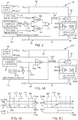
- Fig. 4A is a block diagram that schematically illustrates conversion circuitry 232
- Figs. 4B and 4C are graphs illustrating the operation of the circuitry, according to embodiments of the present invention.
- the purpose of this circuitry is to monitor the operation of the oscillator that generates clock pulses from a clock circuit 272, and to verify that it is within a specific limit.
- the operation of circuitry 232 is generally similar to that of circuitry 132 ( Fig. 3 ), and elements indicated by the same reference numerals in both circuitry 132 and 232 are generally similar in construction and in operation.
- circuitry 232 may be used to monitor voltage levels corresponding to those of the first, second, and third disclosed arrangements referred to above.
- Graph 278A illustrates that the input voltage to the comparator periodically reaches a maximum level 282, then falls to zero.
- comparator 268 is configured to compare its received input voltage with a preset voltage level 284, corresponding to V ref in Fig. 4A , greater than maximum level 282. If maximum 282 is less than level 284, then the comparator outputs a '0' to PU 60. This is illustrated in a graph 286A of the output of comparator, showing that the comparator output is '0'.
- an out-of-range level is output as a threshold-crossing indication to PU 60 if a voltage of the power supply is less than a lower threshold, which is typically less than 1.5 volts.
- the lower threshold may be set to be within a range of 0.2 volts to 0.6 volts.
- the out-of-range signal is output as a threshold-crossing indication to PU 60 if a voltage of the power supply is less than a lower threshold, which is typically less than 1.5 volts.
- the lower threshold may be a value that is between 0.2 volts and 0.6 volts.
- the processing unit By controlling which elements of circuitry 332 continue to receive adequate power (in this case the volatile memory) when the available power is reduced, typically when the voltage driving circuitry 332 reduces to a few tenths of a volt, the processing unit ensures that when the available power enables the channels of module 334 to resume full operation, the data in the memory is effectively instantly available for the operation of the channels.
- circuit element 336 comprises a volatile memory
- the element comprises other circuitry such as control logic.
- Each channel 34 is assumed to have a respective electrode driver, so that channel 34M has a driver 36M3 in its set of elements 36M.
- Driver 36M3 is connected to an electrode 434 which, by way of example, is assumed to be coupled to retinal tissue 24 and to be in proximity to optic nerve 21 ( Fig. 1 ).
- the processing unit may be configured to transmit a PU CTRL signal to one or more channels 34.
- the out-of-range signal may be output as a threshold-crossing indication to PU 60 if a voltage of the power supply is less than a lower threshold, which is typically less than 1.5 volts.
- the lower threshold may be set to be within a range of 0.4 volts to 0.8 volts.
- circuitry 432 By clamping electrodes to the local ground potential, circuitry 432 prevents the possibility of unbalanced pulses being transmitted to the electrodes.
- the channels may be configured to have power down circuitry that reduces the current consumption of the module significantly.
- the reduced current consumption maintains a reduced number of active channels at, for example, less than 40% of the total number of channels.
- the reduced current consumption maintains a reduced number of active channels at less than 15% of the total number of channels. In this manner, for example, even though there may be insufficient power available to drive all of the electrodes of a retinal prosthesis to apply pulses to a patient's retina, at least a small number of the electrodes continue to operate and apply pulses to the retina.
- channels 34 of operating circuitry 62 are assumed to be divided into two sets of channel operating modules: a first operating module set 534 having channels such as channel 34C, and a second operating module set 536 having channels such as channel 34D.
- the two modules are controlled by PU 60, so are effectively coupled together.
- Each operating module is assumed to be powered separately, via respective power controls 538 and 540 which are operated by PU 60, from power supply 38.
- a division of channels in such a manner may be implemented for central and peripheral light sensing elements 30 and their respective channels 34 ( Fig. 1 ).
- first set 534 is assumed to have its power reduced by PU 60 before second set 536.
- the processing unit may wait a second preset time interval, prior to activating power control 538 to increase power to module 534.
- the second time interval is typically but not necessarily longer than the preset time interval that precedes power reduction to module 534.
- the out-of-range signal may be output as a threshold-crossing indication to the processing unit if a voltage of the power supply is less than a lower threshold, which is typically less than 1.5 volts.
- a lower threshold may be between 0.2 volts to 0.6 volts, or 0.4 volts to 0.8 volts.
- Memory 600 ( Fig. 8 ) comprises a p-type and an n-type field effect transistor (FET), p1 and n1, which are connected to form a first inverter.
- FET field effect transistor
- the gates of p1 and n1 are connected to each other and to a " Q " data line.
- the source of n1 is connected to the drain of p1 and to a "Q" data line, the source of p1 is connected to power rail V DD , and the drain of n1 is connected to ground rail GND.
- capacitor c1 begins to discharge through the FET, p3 or p4, conducting at the time when the power supply is below the voltage in floating line 602.
- the out of specification situation typically occurs when V DD is a few tens or hundreds of millivolts.
- the out of specification situation may occur when V DD is below V MIN ( Fig. 1B and Fig. 2B ), for example below the value of V MIN of the first, second or third disclosed arrangements described above in reference to Fig. 1B .
- the discharge maintains the potential of the line Q or Q which is receiving the charge from plate 604, until the capacitor has completely discharged.
- Data loading circuitry 650 applies a condition to the data loading that may be implemented during powering up of a circuit.
- the data loading circuitry is assumed to be comprised in conversion circuitry 332 ( Fig. 5 ).
- the data loading circuitry comprises a volatile configuration register 652 (which is typically part of volatile memory 336) as well as default configuration code data 654 and default error correction code data 656 which are typically stored in a non-volatile manner in operating circuitry 62.
- Configuration code data 654 defines a configuration of the circuit being powered up.
Landscapes
- Engineering & Computer Science (AREA)
- Health & Medical Sciences (AREA)
- Theoretical Computer Science (AREA)
- Physics & Mathematics (AREA)
- General Physics & Mathematics (AREA)
- General Engineering & Computer Science (AREA)
- Animal Behavior & Ethology (AREA)
- General Health & Medical Sciences (AREA)
- Public Health (AREA)
- Veterinary Medicine (AREA)
- Microelectronics & Electronic Packaging (AREA)
- Life Sciences & Earth Sciences (AREA)
- Radiology & Medical Imaging (AREA)
- Nuclear Medicine, Radiotherapy & Molecular Imaging (AREA)
- Biomedical Technology (AREA)
- Power Engineering (AREA)
- Ophthalmology & Optometry (AREA)
- Computer Hardware Design (AREA)
- Dc-Dc Converters (AREA)
- Power Sources (AREA)
- Nonlinear Science (AREA)
- Electromagnetism (AREA)
- Radar, Positioning & Navigation (AREA)
- Automation & Control Theory (AREA)
Claims (12)
- Appareil comprenant : une alimentation (38) ; et
un ensemble de circuits de surveillance de puissance (264), configuré pour surveiller une tension fournie par l'alimentation (38), et comprenant :un circuit d'horloge (272) configuré pour générer un signal d'horloge à l'aide d'une puissance fournie par l'alimentation (38) ;un condensateur (266) configuré pour recevoir un courant de charge fixe, de façon à charger le condensateur (266) ;un dispositif de commutation (270), raccordé au condensateur (266), configuré pour décharger périodiquement le condensateur (266) ; etun comparateur (268), configuré pour effectuer une comparaison d'une tension développée par le condensateur (266) avec une tension seuil, caractérisé en ce que :le dispositif de commutation (270) est configuré pour décharger périodiquement le condensateur (266) en réponse à la réception du signal d'horloge ; etle comparateur (268) est en outre configuré pour délivrer en sortie une indication d'une réduction de tension dans la puissance fournie par l'alimentation (38) lorsque le dispositif de commutation (270) cesse de décharger périodiquement le condensateur (266). - Appareil selon la revendication 1, ledit ensemble de circuits comprenant un générateur de courant constant fournissant le courant de charge fixe.
- Appareil selon la revendication 1, dans ladite tension seuil étant déterminée en réponse à un niveau atteint par le condensateur (266) si le condensateur (266) n'est pas déchargé.
- Appareil selon la revendication 1, ledit comparateur (268) étant conçu pour délivrer en sortie l'indication si une tension de l'alimentation (38) est inférieure à un seuil inférieur.
- Appareil selon la revendication 4, ledit comparateur (268) étant conçu pour délivrer en sortie l'indication si la tension de l'alimentation (38) est inférieure au seuil inférieur, ledit seuil inférieur étant inférieur à 1,5 volt.
- Appareil selon la revendication 5, ledit comparateur (268) étant conçu pour délivrer en sortie l'indication si la tension de l'alimentation (38) est inférieure au seuil inférieur, ledit seuil inférieur étant compris entre 0,2 et 0,6 volts.
- Procédé permettant la surveillance d'une alimentation (38), le procédé comprenant :la fourniture d'une alimentation ; etla configuration d'un ensemble de circuits de surveillance d'une puissance pour surveiller une tension fournie par l'alimentation, en :configurant un circuit d'horloge pour générer un signal d'horloge à l'aide d'une puissance fournie par l'alimentation ;configurant un condensateur (266) pour recevoir un courant de charge fixe, de façon à charger le condensateur (266) ; eten configurant un comparateur pour effectuer une comparaison d'une tension développée par le condensateur avec une tension seuil ; caractérisé par :la configuration d'un dispositif de commutation pour décharger périodiquement le condensateur (266) en réponse à la réception du signal d'horloge ; etla configuration en outre du comparateur pour qu'il délivre en sortie une indication de réduction de tension dans la puissance fournie par l'alimentation lorsque le dispositif de commutation cesse de décharger périodiquement le condensateur (266).
- Procédé selon la revendication 7, ledit courant de charge fixe étant fourni par un générateur de courant constant.
- Procédé selon la revendication 7, ladite tension seuil étant déterminée en réponse à un niveau atteint par le condensateur (266) si le condensateur (266) n'est pas déchargé.
- Procédé selon la revendication 7, ladite émission en sortie de l'indication comprenant l'émission en sortie de l'indication si une tension de l'alimentation (38) est inférieure à un seuil inférieur.
- Procédé selon la revendication 10, ladite émission en sortie l'indication comprenant l'émission en sortie de l'indication si la tension de l'alimentation (38) est inférieure au seuil inférieur, ledit seuil inférieur étant inférieur à 1,5 volts.
- Procédé selon la revendication 11, ladite émission en sortie de l'indication comprenant l'émission en sortie de l'indication si la tension de l'alimentation (38) est inférieure au seuil inférieur, ledit seuil inférieur étant compris entre 0,2 et 0,6 volts.
Applications Claiming Priority (2)
| Application Number | Priority Date | Filing Date | Title |
|---|---|---|---|
| US13/683,158 US9720477B2 (en) | 2012-11-21 | 2012-11-21 | Weak power supply operation and control |
| PCT/IB2013/060270 WO2014080343A1 (fr) | 2012-11-21 | 2013-11-20 | Fonctionnement et commande à faible alimentation |
Publications (3)
| Publication Number | Publication Date |
|---|---|
| EP2922595A1 EP2922595A1 (fr) | 2015-09-30 |
| EP2922595A4 EP2922595A4 (fr) | 2017-02-22 |
| EP2922595B1 true EP2922595B1 (fr) | 2020-01-01 |
Family
ID=50729101
Family Applications (1)
| Application Number | Title | Priority Date | Filing Date |
|---|---|---|---|
| EP13856857.1A Active EP2922595B1 (fr) | 2012-11-21 | 2013-11-20 | Fonctionnement et commande à faible alimentation |
Country Status (3)
| Country | Link |
|---|---|
| US (1) | US9720477B2 (fr) |
| EP (1) | EP2922595B1 (fr) |
| WO (1) | WO2014080343A1 (fr) |
Families Citing this family (10)
| Publication number | Priority date | Publication date | Assignee | Title |
|---|---|---|---|---|
| US10121533B2 (en) | 2012-11-21 | 2018-11-06 | Nano-Retina, Inc. | Techniques for data retention in memory cells during power interruption |
| JP6179276B2 (ja) * | 2013-08-28 | 2017-08-16 | 富士通株式会社 | 情報処理装置及び電源監視回路 |
| US9331791B2 (en) | 2014-01-21 | 2016-05-03 | Nano Retina Ltd. | Transfer of power and data |
| US10119999B2 (en) * | 2014-12-01 | 2018-11-06 | Infineon Technologies Americas Corp. | Circuit connectivity and conveyance of power status information |
| WO2017100545A1 (fr) | 2015-12-10 | 2017-06-15 | Nano-Retina, Inc. | Techniques de rétention de données dans des cellules mémoire pendant une coupure de courant |
| US10226625B2 (en) | 2016-11-03 | 2019-03-12 | Nano Retina Ltd. | Surgical techniques for implantation of a retinal implant |
| US10272244B2 (en) | 2016-11-03 | 2019-04-30 | Nano Retina Ltd. | Retinal implant fixation |
| US10583283B2 (en) | 2018-01-31 | 2020-03-10 | Nano-Retina, Inc. | Retinal implant with image registration |
| CN116859291A (zh) * | 2022-03-28 | 2023-10-10 | 长鑫存储技术有限公司 | 电源映射检测方法、装置、电子设备及介质 |
| US11892520B2 (en) | 2022-03-28 | 2024-02-06 | Changxin Memory Technologies, Inc. | Method and device for power supply mapping detection, electronic device, and medium |
Family Cites Families (62)
| Publication number | Priority date | Publication date | Assignee | Title |
|---|---|---|---|---|
| JPS5429639A (en) | 1977-08-09 | 1979-03-05 | Ricoh Co Ltd | Mulistylus electrostatic recording method |
| US4197850A (en) | 1978-11-03 | 1980-04-15 | Pacesetter Systems, Inc. | Implantable human tissue stimulator with memory protect means |
| US4324252A (en) | 1980-08-04 | 1982-04-13 | Medtronic, Inc. | Memory control circuitry for implantable medical devices |
| US4628933A (en) | 1985-07-23 | 1986-12-16 | Michelson Robin P | Method and apparatus for visual prosthesis |
| US4827261A (en) * | 1987-11-04 | 1989-05-02 | Trofimenkoff Frederick N | Clock-controlled pulse width modulator |
| US4825350A (en) * | 1988-07-21 | 1989-04-25 | General Electric Company | Method and apparatus for detecting a reduction in the input voltage to a power supply |
| US5314458A (en) | 1990-06-01 | 1994-05-24 | University Of Michigan | Single channel microstimulator |
| US5313642A (en) * | 1990-10-03 | 1994-05-17 | Seagull Scientific Systems, Inc. | Power interface for peripheral devices |
| US5769875A (en) | 1994-09-06 | 1998-06-23 | Case Western Reserve University | Functional neuromusclar stimulation system |
| US5834215A (en) | 1994-10-05 | 1998-11-10 | The Administrators Of The Tulane Educational Fund | Method for detecting antipolymer antibodies and diagnosing silicone related disease (SRD) fibromyalgia and chronic fatigue syndrome (CFS) |
| DE69632272T2 (de) | 1995-06-06 | 2005-06-23 | Optobionics Corp., Naperville | Retinal-implantat aus mehrphasigen mikrofotodioden |
| US5712795A (en) * | 1995-10-02 | 1998-01-27 | Alaris Medical Systems, Inc. | Power management system |
| CA2235216C (fr) | 1995-10-19 | 2006-05-30 | The University Of Melbourne | Liaison de donnees integrees et protocole associe |
| JP3633092B2 (ja) * | 1996-03-18 | 2005-03-30 | 日産自動車株式会社 | マイコン故障監視装置 |
| DE19639644A1 (de) * | 1996-09-26 | 1998-04-02 | Siemens Ag | Verfahren und Anordnung zur Steuerung von Funktionen in einer programmgesteuerten Schaltungsanordnung bei Ausfall der Betriebsspannung |
| US5735882A (en) | 1996-11-25 | 1998-04-07 | Sulzer Intermedics Inc. | Cardiac stimulator with backup-mode self-recovery |
| US6035236A (en) | 1998-07-13 | 2000-03-07 | Bionergy Therapeutics, Inc. | Methods and apparatus for electrical microcurrent stimulation therapy |
| US6507758B1 (en) | 1999-03-24 | 2003-01-14 | Second Sight, Llc | Logarithmic light intensifier for use with photoreceptor-based implanted retinal prosthetics and those prosthetics |
| DE60042155D1 (de) | 1999-03-24 | 2009-06-18 | Second Sight Medical Prod Inc | Retinale farbprothese zur wiederherstellung des farbsehens |
| JP3685956B2 (ja) | 1999-06-11 | 2005-08-24 | 住友重機械工業株式会社 | 眼球照射線の制御装置 |
| US6888571B1 (en) | 1999-09-27 | 2005-05-03 | Casio Computer Co., Ltd. | Photosensor system and drive control method thereof |
| DE19948903C2 (de) * | 1999-10-11 | 2002-07-18 | Infineon Technologies Ag | Getaktete Stromversorgung |
| US6389317B1 (en) | 2000-03-31 | 2002-05-14 | Optobionics Corporation | Multi-phasic microphotodetector retinal implant with variable voltage and current capability |
| JP2004521673A (ja) | 2000-11-16 | 2004-07-22 | ポリヴァロール ソシエテ オン コマンディテ | 体内電子インプラントとその人工視覚システム |
| DE10296600T5 (de) | 2001-03-30 | 2004-04-22 | Nidek Co., Ltd. | Kunstaugenvorrichtung |
| JP3883126B2 (ja) | 2001-10-26 | 2007-02-21 | 富士通株式会社 | 半導体集積回路装置、それが組み込まれた電子装置、及び消費電力低減方法 |
| US6976998B2 (en) | 2002-01-17 | 2005-12-20 | Massachusetts Institute Of Technology | Minimally invasive retinal prosthesis |
| KR20040088570A (ko) | 2002-03-05 | 2004-10-16 | 코닌클리케 필립스 일렉트로닉스 엔.브이. | 데이터의 올바르지 않은 저장을 방지하는 제품과 방법 |
| JP4138407B2 (ja) | 2002-08-30 | 2008-08-27 | 株式会社ニデック | 眼内埋殖装置 |
| TW576964B (en) * | 2002-11-22 | 2004-02-21 | Wistron Corp | Method and related computer for processing suspend to RAM during power off |
| US7047080B2 (en) | 2003-02-14 | 2006-05-16 | The Board Of Trustees Of The Leland Stanford Junior University | Self-sufficient retinal prosthesis powered by intraocular photovoltaic cells |
| WO2004084582A1 (fr) | 2003-03-17 | 2004-09-30 | Microsound A/S | Prothese auditive comprenant des informations relatives a la batterie rechargeable |
| DE10315397A1 (de) | 2003-04-04 | 2004-10-14 | Carl Zeiss | Energieversorgungsvorrichtung für ein Retina-Implantat |
| US7311723B2 (en) | 2003-07-11 | 2007-12-25 | University Of Washington | Scanning laser device and methods of use |
| WO2005072667A1 (fr) | 2004-01-29 | 2005-08-11 | Konica Minolta Photo Imaging, Inc. | Dispositif d'affichage pour vision auxiliaire |
| FR2868218A1 (fr) * | 2004-03-23 | 2005-09-30 | Jean Michel Cour | Methode et dispositif de charge de batterie par impulsions tolerant les fluctuations d'une source de courant continu |
| JP4767571B2 (ja) | 2005-03-31 | 2011-09-07 | 株式会社ニデック | 視覚再生補助装置 |
| US7342427B1 (en) | 2005-12-19 | 2008-03-11 | National Semiconductor Corporation | Automatic clock based power-down circuit |
| US7610098B2 (en) | 2005-12-20 | 2009-10-27 | Imi Intelligent Medical Implants Ag | Charge-integrating retinal prosthesis and method |
| US20110254661A1 (en) | 2005-12-23 | 2011-10-20 | Invue Security Products Inc. | Programmable security system and method for protecting merchandise |
| WO2007091211A2 (fr) | 2006-02-09 | 2007-08-16 | Nxp B.V. | Agencement de circuit et procédé de détection d'une situation de coupure d'une source d'alimentation en tension |
| CN100484498C (zh) | 2006-04-19 | 2009-05-06 | 华中科技大学 | 一种柔性视网膜芯片及其制备方法 |
| US8000804B1 (en) | 2006-10-27 | 2011-08-16 | Sandia Corporation | Electrode array for neural stimulation |
| US8660660B2 (en) | 2006-11-14 | 2014-02-25 | Second Sight Medical Products, Inc. | Power scheme for implant stimulators on the human or animal body |
| US7831309B1 (en) | 2006-12-06 | 2010-11-09 | University Of Southern California | Implants based on bipolar metal oxide semiconductor (MOS) electronics |
| US7635983B2 (en) * | 2007-01-09 | 2009-12-22 | Myers Power Products, Inc. | Battery testing apparatus that controls a switch to allow current to flow from the battery to a utility power source |
| EP2265171B1 (fr) | 2008-03-12 | 2016-03-09 | The Trustees of the University of Pennsylvania | Réseau de capteurs flexibles et pouvant être mis à l'échelle pour enregistrer et moduler une activité physiologique |
| US9089701B2 (en) | 2008-09-18 | 2015-07-28 | Second Sight Medical Products, Inc. | Techniques and functional electrical stimulation to eliminate discomfort during electrical stimulation of the retina |
| US8428740B2 (en) | 2010-08-06 | 2013-04-23 | Nano-Retina, Inc. | Retinal prosthesis techniques |
| US8150526B2 (en) | 2009-02-09 | 2012-04-03 | Nano-Retina, Inc. | Retinal prosthesis |
| US8718784B2 (en) | 2010-01-14 | 2014-05-06 | Nano-Retina, Inc. | Penetrating electrodes for retinal stimulation |
| US8706243B2 (en) | 2009-02-09 | 2014-04-22 | Rainbow Medical Ltd. | Retinal prosthesis techniques |
| US8442641B2 (en) | 2010-08-06 | 2013-05-14 | Nano-Retina, Inc. | Retinal prosthesis techniques |
| US9444213B2 (en) | 2009-03-09 | 2016-09-13 | Nucurrent, Inc. | Method for manufacture of multi-layer wire structure for high efficiency wireless communication |
| US20100249878A1 (en) | 2009-03-27 | 2010-09-30 | Mcmahon Matthew J | Visual Prosthesis Fitting Training and Assessment System and Method |
| US8421479B2 (en) | 2009-06-30 | 2013-04-16 | Navisense | Pulsed echo propagation device and method for measuring a parameter |
| US8939579B2 (en) | 2011-01-28 | 2015-01-27 | Light Prescriptions Innovators, Llc | Autofocusing eyewear, especially for presbyopia correction |
| CN106902457B (zh) | 2011-01-28 | 2022-10-21 | 斯蒂维科技公司 | 神经刺激器系统 |
| US8571669B2 (en) | 2011-02-24 | 2013-10-29 | Nano-Retina, Inc. | Retinal prosthesis with efficient processing circuits |
| KR20120120706A (ko) * | 2011-04-25 | 2012-11-02 | 삼성전자주식회사 | 보조 전원 장치 및 보조 전원 장치를 포함하는 사용자 장치 |
| GB2496379A (en) | 2011-11-04 | 2013-05-15 | Univ Edinburgh | A freespace optical communication system which exploits the rolling shutter mechanism of a CMOS camera |
| CA2874899C (fr) | 2012-06-01 | 2017-07-11 | Blackberry Limited | Moteur de synchronisation universel base sur des methodes probabilistes pour garantir le verrouillage de systemes audio multiformat |
-
2012
- 2012-11-21 US US13/683,158 patent/US9720477B2/en active Active
-
2013
- 2013-11-20 EP EP13856857.1A patent/EP2922595B1/fr active Active
- 2013-11-20 WO PCT/IB2013/060270 patent/WO2014080343A1/fr active Application Filing
Non-Patent Citations (1)
| Title |
|---|
| None * |
Also Published As
| Publication number | Publication date |
|---|---|
| US20140143559A1 (en) | 2014-05-22 |
| US9720477B2 (en) | 2017-08-01 |
| EP2922595A1 (fr) | 2015-09-30 |
| WO2014080343A1 (fr) | 2014-05-30 |
| EP2922595A4 (fr) | 2017-02-22 |
Similar Documents
| Publication | Publication Date | Title |
|---|---|---|
| EP2922595B1 (fr) | Fonctionnement et commande à faible alimentation | |
| TW513839B (en) | Charge circuit that performs charge control by comparing a plurality of battery voltages | |
| US9729145B2 (en) | Circuit and a method for selecting a power supply | |
| US10447053B2 (en) | Terminal | |
| US20080054855A1 (en) | Circuits and methods for controlling power in a battery operated system | |
| ES2662000T3 (es) | Terminal móvil capaz de restaurar una aplicación después de un reinicio | |
| US9814882B2 (en) | Rechargeable-battery implantable medical device having a primary battery active during a rechargeable-battery undervoltage condition | |
| US9806612B2 (en) | Systems and methods of energy saving in a battery charging system | |
| CN111987772B (zh) | 一种片上系统、电池组件及电子装置 | |
| US9242109B2 (en) | Apparatus and methods facilitating power regulation for an implantable device | |
| US9026211B2 (en) | Battery charger circuit for battery powered implantable neurostimulation systems | |
| JP2016538907A (ja) | 埋込可能な医療デバイスのための電源切断電流測定 | |
| JP2018011442A (ja) | 受電装置およびその制御回路、電子機器、給電システムの動作方法 | |
| JPH09288897A (ja) | 電圧供給回路 | |
| CN111987773B (zh) | 一种片上系统、电池组件及电子装置 | |
| KR19990088544A (ko) | 전지상태감시회로및전지장치 | |
| US10121533B2 (en) | Techniques for data retention in memory cells during power interruption | |
| CN113453108B (zh) | 无线耳机、无线耳机系统和无线耳机的关机方法 | |
| AU2015277295A1 (en) | Voltage regulator and control circuit for silver-zinc batteries in hearing instruments | |
| EP3316385B1 (fr) | Système de batterie avec horloge en temps réel à alimentation interne, circuit d'alimentation électrique pour une horloge en temps réel et procédé pour faire fonctionner une horloge en temps réel d'un système de batterie | |
| US20080122527A1 (en) | Semiconductor integrated circuit device having internal voltage generating circuit | |
| US9463328B2 (en) | Nanopower voltage reference for an implantable medical device | |
| US9238148B2 (en) | Method for increasing buck regulator efficiency using charge recapturing in an implantable cardiac device | |
| JP6143819B2 (ja) | 定電圧回路及び電源システム | |
| US10069059B2 (en) | Method and apparatus for shake awake smart battery pack |
Legal Events
| Date | Code | Title | Description |
|---|---|---|---|
| PUAI | Public reference made under article 153(3) epc to a published international application that has entered the european phase |
Free format text: ORIGINAL CODE: 0009012 |
|
| 17P | Request for examination filed |
Effective date: 20150610 |
|
| AK | Designated contracting states |
Kind code of ref document: A1 Designated state(s): AL AT BE BG CH CY CZ DE DK EE ES FI FR GB GR HR HU IE IS IT LI LT LU LV MC MK MT NL NO PL PT RO RS SE SI SK SM TR |
|
| AX | Request for extension of the european patent |
Extension state: BA ME |
|
| DAX | Request for extension of the european patent (deleted) | ||
| RA4 | Supplementary search report drawn up and despatched (corrected) |
Effective date: 20170123 |
|
| RIC1 | Information provided on ipc code assigned before grant |
Ipc: G11C 5/14 20060101ALI20170117BHEP Ipc: G06F 1/28 20060101ALI20170117BHEP Ipc: A61N 1/36 20060101AFI20170117BHEP Ipc: A61N 1/378 20060101ALI20170117BHEP Ipc: G06F 1/32 20060101ALI20170117BHEP |
|
| STAA | Information on the status of an ep patent application or granted ep patent |
Free format text: STATUS: EXAMINATION IS IN PROGRESS |
|
| 17Q | First examination report despatched |
Effective date: 20180419 |
|
| GRAP | Despatch of communication of intention to grant a patent |
Free format text: ORIGINAL CODE: EPIDOSNIGR1 |
|
| STAA | Information on the status of an ep patent application or granted ep patent |
Free format text: STATUS: GRANT OF PATENT IS INTENDED |
|
| INTG | Intention to grant announced |
Effective date: 20190724 |
|
| GRAS | Grant fee paid |
Free format text: ORIGINAL CODE: EPIDOSNIGR3 |
|
| GRAA | (expected) grant |
Free format text: ORIGINAL CODE: 0009210 |
|
| STAA | Information on the status of an ep patent application or granted ep patent |
Free format text: STATUS: THE PATENT HAS BEEN GRANTED |
|
| AK | Designated contracting states |
Kind code of ref document: B1 Designated state(s): AL AT BE BG CH CY CZ DE DK EE ES FI FR GB GR HR HU IE IS IT LI LT LU LV MC MK MT NL NO PL PT RO RS SE SI SK SM TR |
|
| REG | Reference to a national code |
Ref country code: GB Ref legal event code: FG4D |
|
| REG | Reference to a national code |
Ref country code: CH Ref legal event code: EP Ref country code: AT Ref legal event code: REF Ref document number: 1219023 Country of ref document: AT Kind code of ref document: T Effective date: 20200115 |
|
| REG | Reference to a national code |
Ref country code: IE Ref legal event code: FG4D |
|
| REG | Reference to a national code |
Ref country code: DE Ref legal event code: R096 Ref document number: 602013064718 Country of ref document: DE |
|
| REG | Reference to a national code |
Ref country code: NL Ref legal event code: MP Effective date: 20200101 |
|
| REG | Reference to a national code |
Ref country code: LT Ref legal event code: MG4D |
|
| PG25 | Lapsed in a contracting state [announced via postgrant information from national office to epo] |
Ref country code: CZ Free format text: LAPSE BECAUSE OF FAILURE TO SUBMIT A TRANSLATION OF THE DESCRIPTION OR TO PAY THE FEE WITHIN THE PRESCRIBED TIME-LIMIT Effective date: 20200101 Ref country code: PT Free format text: LAPSE BECAUSE OF FAILURE TO SUBMIT A TRANSLATION OF THE DESCRIPTION OR TO PAY THE FEE WITHIN THE PRESCRIBED TIME-LIMIT Effective date: 20200527 Ref country code: NO Free format text: LAPSE BECAUSE OF FAILURE TO SUBMIT A TRANSLATION OF THE DESCRIPTION OR TO PAY THE FEE WITHIN THE PRESCRIBED TIME-LIMIT Effective date: 20200401 Ref country code: FI Free format text: LAPSE BECAUSE OF FAILURE TO SUBMIT A TRANSLATION OF THE DESCRIPTION OR TO PAY THE FEE WITHIN THE PRESCRIBED TIME-LIMIT Effective date: 20200101 Ref country code: RS Free format text: LAPSE BECAUSE OF FAILURE TO SUBMIT A TRANSLATION OF THE DESCRIPTION OR TO PAY THE FEE WITHIN THE PRESCRIBED TIME-LIMIT Effective date: 20200101 Ref country code: NL Free format text: LAPSE BECAUSE OF FAILURE TO SUBMIT A TRANSLATION OF THE DESCRIPTION OR TO PAY THE FEE WITHIN THE PRESCRIBED TIME-LIMIT Effective date: 20200101 Ref country code: LT Free format text: LAPSE BECAUSE OF FAILURE TO SUBMIT A TRANSLATION OF THE DESCRIPTION OR TO PAY THE FEE WITHIN THE PRESCRIBED TIME-LIMIT Effective date: 20200101 |
|
| PG25 | Lapsed in a contracting state [announced via postgrant information from national office to epo] |
Ref country code: BG Free format text: LAPSE BECAUSE OF FAILURE TO SUBMIT A TRANSLATION OF THE DESCRIPTION OR TO PAY THE FEE WITHIN THE PRESCRIBED TIME-LIMIT Effective date: 20200401 Ref country code: GR Free format text: LAPSE BECAUSE OF FAILURE TO SUBMIT A TRANSLATION OF THE DESCRIPTION OR TO PAY THE FEE WITHIN THE PRESCRIBED TIME-LIMIT Effective date: 20200402 Ref country code: IS Free format text: LAPSE BECAUSE OF FAILURE TO SUBMIT A TRANSLATION OF THE DESCRIPTION OR TO PAY THE FEE WITHIN THE PRESCRIBED TIME-LIMIT Effective date: 20200501 Ref country code: LV Free format text: LAPSE BECAUSE OF FAILURE TO SUBMIT A TRANSLATION OF THE DESCRIPTION OR TO PAY THE FEE WITHIN THE PRESCRIBED TIME-LIMIT Effective date: 20200101 Ref country code: SE Free format text: LAPSE BECAUSE OF FAILURE TO SUBMIT A TRANSLATION OF THE DESCRIPTION OR TO PAY THE FEE WITHIN THE PRESCRIBED TIME-LIMIT Effective date: 20200101 Ref country code: HR Free format text: LAPSE BECAUSE OF FAILURE TO SUBMIT A TRANSLATION OF THE DESCRIPTION OR TO PAY THE FEE WITHIN THE PRESCRIBED TIME-LIMIT Effective date: 20200101 |
|
| REG | Reference to a national code |
Ref country code: DE Ref legal event code: R097 Ref document number: 602013064718 Country of ref document: DE |
|
| PG25 | Lapsed in a contracting state [announced via postgrant information from national office to epo] |
Ref country code: ES Free format text: LAPSE BECAUSE OF FAILURE TO SUBMIT A TRANSLATION OF THE DESCRIPTION OR TO PAY THE FEE WITHIN THE PRESCRIBED TIME-LIMIT Effective date: 20200101 Ref country code: SK Free format text: LAPSE BECAUSE OF FAILURE TO SUBMIT A TRANSLATION OF THE DESCRIPTION OR TO PAY THE FEE WITHIN THE PRESCRIBED TIME-LIMIT Effective date: 20200101 Ref country code: RO Free format text: LAPSE BECAUSE OF FAILURE TO SUBMIT A TRANSLATION OF THE DESCRIPTION OR TO PAY THE FEE WITHIN THE PRESCRIBED TIME-LIMIT Effective date: 20200101 Ref country code: EE Free format text: LAPSE BECAUSE OF FAILURE TO SUBMIT A TRANSLATION OF THE DESCRIPTION OR TO PAY THE FEE WITHIN THE PRESCRIBED TIME-LIMIT Effective date: 20200101 Ref country code: DK Free format text: LAPSE BECAUSE OF FAILURE TO SUBMIT A TRANSLATION OF THE DESCRIPTION OR TO PAY THE FEE WITHIN THE PRESCRIBED TIME-LIMIT Effective date: 20200101 Ref country code: SM Free format text: LAPSE BECAUSE OF FAILURE TO SUBMIT A TRANSLATION OF THE DESCRIPTION OR TO PAY THE FEE WITHIN THE PRESCRIBED TIME-LIMIT Effective date: 20200101 |
|
| PLBE | No opposition filed within time limit |
Free format text: ORIGINAL CODE: 0009261 |
|
| STAA | Information on the status of an ep patent application or granted ep patent |
Free format text: STATUS: NO OPPOSITION FILED WITHIN TIME LIMIT |
|
| REG | Reference to a national code |
Ref country code: AT Ref legal event code: MK05 Ref document number: 1219023 Country of ref document: AT Kind code of ref document: T Effective date: 20200101 |
|
| 26N | No opposition filed |
Effective date: 20201002 |
|
| PG25 | Lapsed in a contracting state [announced via postgrant information from national office to epo] |
Ref country code: IT Free format text: LAPSE BECAUSE OF FAILURE TO SUBMIT A TRANSLATION OF THE DESCRIPTION OR TO PAY THE FEE WITHIN THE PRESCRIBED TIME-LIMIT Effective date: 20200101 Ref country code: AT Free format text: LAPSE BECAUSE OF FAILURE TO SUBMIT A TRANSLATION OF THE DESCRIPTION OR TO PAY THE FEE WITHIN THE PRESCRIBED TIME-LIMIT Effective date: 20200101 |
|
| PG25 | Lapsed in a contracting state [announced via postgrant information from national office to epo] |
Ref country code: SI Free format text: LAPSE BECAUSE OF FAILURE TO SUBMIT A TRANSLATION OF THE DESCRIPTION OR TO PAY THE FEE WITHIN THE PRESCRIBED TIME-LIMIT Effective date: 20200101 Ref country code: PL Free format text: LAPSE BECAUSE OF FAILURE TO SUBMIT A TRANSLATION OF THE DESCRIPTION OR TO PAY THE FEE WITHIN THE PRESCRIBED TIME-LIMIT Effective date: 20200101 |
|
| PG25 | Lapsed in a contracting state [announced via postgrant information from national office to epo] |
Ref country code: MC Free format text: LAPSE BECAUSE OF FAILURE TO SUBMIT A TRANSLATION OF THE DESCRIPTION OR TO PAY THE FEE WITHIN THE PRESCRIBED TIME-LIMIT Effective date: 20200101 |
|
| REG | Reference to a national code |
Ref country code: CH Ref legal event code: PL |
|
| PG25 | Lapsed in a contracting state [announced via postgrant information from national office to epo] |
Ref country code: LU Free format text: LAPSE BECAUSE OF NON-PAYMENT OF DUE FEES Effective date: 20201120 |
|
| REG | Reference to a national code |
Ref country code: BE Ref legal event code: MM Effective date: 20201130 |
|
| PG25 | Lapsed in a contracting state [announced via postgrant information from national office to epo] |
Ref country code: CH Free format text: LAPSE BECAUSE OF NON-PAYMENT OF DUE FEES Effective date: 20201130 Ref country code: LI Free format text: LAPSE BECAUSE OF NON-PAYMENT OF DUE FEES Effective date: 20201130 |
|
| PG25 | Lapsed in a contracting state [announced via postgrant information from national office to epo] |
Ref country code: IE Free format text: LAPSE BECAUSE OF NON-PAYMENT OF DUE FEES Effective date: 20201120 |
|
| PG25 | Lapsed in a contracting state [announced via postgrant information from national office to epo] |
Ref country code: TR Free format text: LAPSE BECAUSE OF FAILURE TO SUBMIT A TRANSLATION OF THE DESCRIPTION OR TO PAY THE FEE WITHIN THE PRESCRIBED TIME-LIMIT Effective date: 20200101 Ref country code: MT Free format text: LAPSE BECAUSE OF FAILURE TO SUBMIT A TRANSLATION OF THE DESCRIPTION OR TO PAY THE FEE WITHIN THE PRESCRIBED TIME-LIMIT Effective date: 20200101 Ref country code: CY Free format text: LAPSE BECAUSE OF FAILURE TO SUBMIT A TRANSLATION OF THE DESCRIPTION OR TO PAY THE FEE WITHIN THE PRESCRIBED TIME-LIMIT Effective date: 20200101 |
|
| PG25 | Lapsed in a contracting state [announced via postgrant information from national office to epo] |
Ref country code: MK Free format text: LAPSE BECAUSE OF FAILURE TO SUBMIT A TRANSLATION OF THE DESCRIPTION OR TO PAY THE FEE WITHIN THE PRESCRIBED TIME-LIMIT Effective date: 20200101 Ref country code: AL Free format text: LAPSE BECAUSE OF FAILURE TO SUBMIT A TRANSLATION OF THE DESCRIPTION OR TO PAY THE FEE WITHIN THE PRESCRIBED TIME-LIMIT Effective date: 20200101 |
|
| PG25 | Lapsed in a contracting state [announced via postgrant information from national office to epo] |
Ref country code: BE Free format text: LAPSE BECAUSE OF NON-PAYMENT OF DUE FEES Effective date: 20201130 |
|
| PGFP | Annual fee paid to national office [announced via postgrant information from national office to epo] |
Ref country code: GB Payment date: 20231123 Year of fee payment: 11 |
|
| PGFP | Annual fee paid to national office [announced via postgrant information from national office to epo] |
Ref country code: FR Payment date: 20231120 Year of fee payment: 11 Ref country code: DE Payment date: 20231121 Year of fee payment: 11 |