Adopt the dipole illumination technology to rely on the orientation of shielding
Technical field
The present invention relates to use the photo-mask process of dipole illumination technology, relate in particular to the generation operation of mask layout, this dipole illumination technology is used to reduce the loss of the picture contrast that is caused by lens flare, and this has significant effect under the situation of using dipole illumination owing to multiexposure, multiple exposure.In addition, the invention still further relates to a kind of device producing method that uses lithographic equipment, wherein lithographic equipment comprises a radiating system that the projection radiation light beam is provided; A mask platform of supporting mask is used for the composition projected light beam; A chip bench that is used for support substrate; And projected light beam that is used for projection institute composition optical projection system on the substrate target part.
Background technology
For example, in the manufacture process of integrated circuit (IC), can use lithographic projection apparatus (instrument).In this case, mask comprises a circuitous pattern corresponding to each layer of IC, and the target that this figure can be imaged at substrate (for example, being not limited in silicon wafer) (for example partly goes up, comprise one or more matrixs), this substrate has been coated with one deck radiation-sensitive material (resist).Usually, silicon wafer will comprise the whole array of adjacent target part, target partly pass through optical projection system one next by continuous radiation.In one type lithographic projection apparatus, by whole reticle figure being exposing to target each the target part of radiation of partly coming up.The so-called wafer stepper of this equipment.In the equipment of a replacement-be commonly referred to that stepping-scanning device-by the mask graph of lining by line scan under the projected light beam of specifying reference direction (scanning direction) at, synchronous scanning simultaneously comes each target part of radiation in the method for or antiparallel chip bench parallel with this direction; Usually, because optical projection system has a magnification M (usually<1), the speed V of scanning substrate platform will be the multiple of coefficient M, and mask platform will scan with this speed.Here narration can be about the more information of lithographic equipment from for example US6, collect in 046,792, be incorporated herein by reference.
In using the manufacture process of lithographic projection apparatus, mask graph is imaged at one to the substrate that is covered by radiation-sensitive material layer (resist) of small part.Before image-forming step, this substrate can carry out various processing, such as priming operation, and resist plated film, soft baking etc.After exposure, substrate can carry out other processing, such as post exposure bake (PEB), develop, cures with the mensuration/check of imaging features firmly etc.It is as basis such as each layer of IC equipment of composition that such processing is arranged.This then patterned layer can carry out various processing, and such as etching, ion injects (doping), metallising, and oxidation, chemistry-mechanical polishing etc., these all processes will finish the processing of individual layer.Carry out a plurality of layers processing if desired, so whole process or its variation will be carried out repeated operation to each new layer and handle.At last, the array of a device will be presented on the substrate (wafer).Then by using technology that these devices are separated from each other such as cutting or sawing.After this, single assembly just can be installed to carrier, is connected to pin or the like.More information about this processing can be obtained from the book such as " microchip is made: semiconductor technology is guided (MicrochipFabrication:A Practical Guide to Semiconductor Processing) ", this book is to be write by Peter van Zant, McGraw Hill publishing company published in 1997 for the third time, ISBN number is 0-07-067250-4, is incorporated herein by reference.
Lithography tool can be the type with two or more chip bench (and/or two or more mask platform).The a plurality of additional stations of use that in this class " multistage " device, can walk abreast, the step of perhaps can be when carrying out exposure-processed for one or more on one or more other platforms, carrying out preparation, for example at US5,969,441 and WO98/40791 in the twin-stage lithography tool narrated, be incorporated herein by reference.
Aforesaid mask comprises corresponding to the geometric pattern that is integrated in the circuit element on the silicon wafer.By using CAD (computer-aided design) program to produce the figure that is used to set up these masks, claim that usually this process is EDA (electric design automation).Most CAD programs all will be followed the predetermined design rule of a cover so that set up the function mask.These rules are by being provided with the qualification of handling and design.For example, he design rules specify the interval tolerance limit between circuit devcie (such as gate circuit, capacitor etc.) or interconnection line can not interact so that guarantee circuit devcie or line in nonconforming mode.
Certainly, a target in the integrated circuit manufacturing is (process mask) accurately to reproduce original circuit design on wafer.Another target is to use semiconductor wafer as much as possible effective coverage.Yet owing to will reduce the size of integrated circuit and increase its density, the CD (critical dimension) of its corresponding mask figure will level off to the resolution limit of optical exposure instrument.Resolution to exposure tool is restricted to the minimum feature that exposure tool can repeat to expose on wafer.The resolution value of current exposure sources can retrain the CD of many improved IC circuit design usually.
And for microelectronic element, in the speed of microprocessor, updating on memory assembling density and the low power consumption will be directly connected to transmits on the semiconductor equipment different layers and the performance of the photoetching technique of formed patterns.Current technology status is the composition that requires the CD below the available light source wavelength.For example, current 248nm produces wavelength and trends towards composition less than 100nm CD.Described in semiconductor international technology road sign (ITRS2000), this industrial trend will continue always and may accelerated development in from now on 5-10 years.
Cause in the development that improves various technology aspect the resolution for the continuous demand that improves performance.This class technology typically is called resolution enhance technology (RET), and comprises application very widely.These examples comprise: light source is revised (for example, the off-axis irradiation), utilize the use (for example, attenuated phase-shifting mask, alternating phase-shift mask, no chrome mask etc.) of the particular mask of light interference phenomena, and (for example optical proximity correction) is revised in mask layout.
In aforesaid technology, the dipole irradiation is one of them the most attractive RET candidate technologies, and this is because he has the hi-vision contrast and have good resolution performance for intensive pitch.As everyone knows, the dipole irradiation is the extreme case of OAI, and it can have the image contrast that improves the enhancing of handling tolerance for low-down K1 imaging provides.
Yet a limitation relevant with the dipole irradiation is that single irradiation only strengthens the resolution perpendicular to the feature of shining field axis.Therefore, in order to utilize the dipole irradiation fully during wafer is printed, mask graph must be decomposed on level and vertical direction.In case mask graph is transformed by this way, the exposure of Y magnetic pole just is used to carry out the imaging of horizontal orientation feature so, and the exposure of X magnetic pole just is used to carry out the imaging of vertical orientation feature.Key character of dipole irradiation is that when carrying out the imaging of horizontal orientation feature the vertical orientation feature must be subjected to protection (conductively-closed just), so that the vertical orientation feature can not cut down.When the vertical orientation feature will be carried out opposite operation (just the horizontal orientation feature must be protected) during by imaging.
Fig. 1 has illustrated the basic principle of double dipole imaging.According to narration, when using the dipole irradiation, typically has double exposure at least.In exposure for the first time, X dipole aperture 10 provides the space image brightness (maximum modulation just) of maximum for the vertical component of the line 12 that will print.Resulting image outline is shown in Fig. 1 center line 24.In the exposure second time of using Y dipole aperture 16, line 12 is not carried out image modulation.Yet, it should be noted that the vertical component of line 12 need be shielded, so that the vertical features that forms between exposure period in the first time can not cut down between exposure period in the second time in second time of using Y dipole aperture between exposure period.Fig. 1 has narrated the shielding conductor 12 that has shielding 15, and each shielding 15 has the width of horizontal direction 20nm.Therefore, when using Y dipole aperture exposure levels line, come down to not have the imaging (modulation just) of vertical features 12.Space image is that it is corresponding to the shielding of 20nm by the modulation of the DC shown in the line among Fig. 1 17.Last space image brightness is corresponding to the sum of the exposure first time of using X dipole aperture with the exposure second time of using Y dipole aperture, and wherein this space image brightness is to be represented by the line among Fig. 1 14.
It is also to be noted that, suppose the energy constant of exposure, increase the shielding width of vertical line 12, will make the minimum brightness rank of gained image transform to lower level from 20nm shielding 15 to 40nm shieldings 20.This represents with line 22 in Fig. 1, its expression space image relevant with the vertical component of feature.Content as shown, space image 22 be a DC modulation just.Yet it is lower than the DC modulation 17 that interrelates with the 20nm shielding.Therefore, use 40nm to shield formed composite image the image effect that is better than using the composite image 14 that the 20nm shielding forms is provided.
Owing to need the feature of separation of level and vertical orientation, when using the dipole irradiation, just be faced with a difficult problem for the lithographer, that is exactly will determine how original IC design data to be transformed on level or the vertical graphic elements, and generating two masks that are used for the double-exposure processing, the performance that can use the dipole imaging is fully handled in this double-exposure.One reduce performance and should considerable factor be in producing the mask images process because lens flare or bias light that scattering caused.As everyone knows, lens flare will cause unwanted bias light (noise just), and it can reduce picture contrast on image plane.Therefore, just wish to reduce as much as possible " hot spot ".This seems particularly true under the situation of using relevant dipole irradiation technique owing to multistage exposure.
" space image that has hot spot " equals by " space image that does not have hot spot " of a scattering function (PSF) convolution and scattering sum.Foregoing can be expressed as:
Wherein TIS is the summation (TIS) to whole scatterings of coarse planar lens with a similar Gaussian Profile.In this case, TIS can be expressed as:
TIS=[(4π?σcosθ)/λ]
2 ......(2)
Wherein λ is the wavelength of exposure tool, and σ is the r.m.s. roughness of lens, and θ is the angle of scattering.Because when the manufacturing property of front lens, it will cause showing the lens of extremely low plane roughness, above-mentioned equation can be approximately:
TIS~1/λ
2 ......(3)
Can see clearly that from equation (3) quantity of scattered light will increase significantly when reducing the wavelength of exposure tool.For example, for the exposure tool with 193nm wavelength, whole scattering summations (TIS) of light approximately are 1.65 times of whole scattering summations with exposure tool of 248nm wavelength.
First that should be noted that equation (1) is " diffuse halation " that causes that focusedimage enlarges.Second effect of scattering due in the equation (1).Whole exercising result is to produce a harmful DC bias light, and it will reduce the contrast of space image.And except the negative effect to picture contrast, hot spot also can unevenly be distributed through scanning slit, and causes the inhomogeneous of the field of exposing, and this will cause the CD in the field to change.Therefore, protection feature and minimizing background stray light just become very crucial.When the wavelength of exposure tool is reduced, how to reduce or the influence of getting rid of background stray light just becomes more important.
Current, a prior art that is used to reduce the hot spot negative effect is included in the large tracts of land mask graph (background parts just) that does not contain any geometric figure (feature just) and goes up the step that increases solid chromium overcoat.Shown in Fig. 2 a and 2b, when using the dipole irradiation, the solid chromium overcoat that is called bias light shielding (BLS) is used in the background area on level mask and the vertical mask.This solid chromium overcoat plays shielding action with the protection background area during double exposing.Fig. 2 a has narrated one and has used this shield technology in conjunction with the example of printing the feature 29 of horizontal orientation by use Y dipole 16.Shown in Fig. 2 a, each vertical features 27 all is provided with the shielding of discussing in conjunction with Fig. 1 210 (just main feature shielding) in the above.In addition, solid chromium overcoat 220 is set on the background area, is not imaged on the feature on the wafer in this background area.In an identical manner, Fig. 2 b has narrated when printing vertical features, the vertical mask that the horizontal orientation feature in the mask is shielded.As implied above, vertical mask also comprises a solid chromium overcoat 220 that is configured on the background area.Note also that level mask and vertical mask all comprise supplemental characteristic 103 (for example scattering strip).
Yet, owing to use this background shielding 220, to such an extent as to the brightness in the background area just becomes very low and can not remove this resist completely when using positive resist.Fig. 3 a and 3b have narrated a simulation corresponding to the mask that is limited by zone 30 among Fig. 2 a and 2b resist figure partly, and wherein zone 30 comprises solid chromium overcoat 220.This simulation is at supposition NA (numerical aperture)=0.75, ArF double-exposure X magnetic pole, and the Y magnetic pole, the condition of σ outer/ σ inner=0.89/0.65 is got off and is carried out.Shown in Fig. 3 a and 3b, by using vertical mask and level mask, the resist part 221 after irradiation in the background area still exists.Therefore, in order from the zone of background shielding, to eliminate resist completely, use a trim mask to expose for the third time with regard to needs.Therefore, the solution of this minimizing hot spot influence is unsatisfactory, because it causes being used for the increase of required exposure frequency of imaging wafer and mask number.With reference to Fig. 3 a, the zone that the zone of being represented by reference number 51 still keeps corresponding to resist after double exposure, and these zones form contrast with the horizontal or vertical masks area that is provided with chromium (any one in feature or the overcoat just).
And, above-mentioned solid chromium shield technology also may adverse influence to supplemental characteristic, such as scattering strip etc., this just makes supplemental characteristic can be printed under level or the vertical mask overcoat, this is also as shown in Fig. 3 a and the 3b.For example, with reference to Fig. 3 b, as shown in the simulation of resist, plan is that the supplemental characteristic 103 of secondary resolution is because BLS220 and printed.This problem has applied an extra restriction to the setting of supplemental characteristic, and this has just hindered the setting of supplemental characteristic on the optimum position, thereby has reduced the performance of printing.
Therefore, just need provide a kind of method that can eliminate the hot spot influence in the process of exposure, it can not cause the increase that is used for required exposure frequency of imaging wafer and mask number, can not influence the use and/or the placement of supplemental characteristic in the mask yet.
Summary of the invention
In the effort that solves the demand, an object of the present invention is to provide a kind of shield technology, this technology can't cause being used for the increase of required exposure frequency of imaging wafer and mask number, also can not influence use and/or setting about the supplemental characteristic of mask design.
More clearly, in one embodiment, the present invention relates to a kind of dipole that uses and be radiated at the method for printing the figure with vertical orientation feature and horizontal orientation feature on the substrate, it comprises step: identification is included in the background area in the figure; Produce a perpendicular elements mask that comprises the horizontal orientation feature that to differentiate in the background area; Produce a horizontal cell mask that comprises the vertical orientation feature that to differentiate in the background area; Use the X magnetic pole to shine described vertical component mask; And use the Y magnetic pole to shine described horizontal cell mask.As the content of being narrated hereinafter, the feature that can not differentiate is attached to the background parts of mask graph, so that reduce the bias light incide on the wafer and the influence of cancellation lens flare.
Though the specific reference of this paper setting is the use of the present invention in IC makes, the present invention that recognizes who should be understood that can have other application.For example, it can be applied in integrated optics system, be used for the guiding of magnetic domain storage and test pattern, the manufacturing of LCD panel, film magnetic head etc., those of ordinary skill in the art can recognize in these selectable applied environments, any term " reticle " of Shi Yonging in this article, " wafer " and " matrix " will be understood that and can be replaced by more general term " mask ", " substrate " and " target part " respectively.
In the text, employed term " radiation " and " light beam " have comprised all types of electromagnetic radiation, electromagnetic radiation comprise ultraviolet radiation (for example wavelength be 365,248,193,157 or 126nm) and EUV (far-ultraviolet region radiation, for example wavelength is in the scope of 5-20nm).
Employed in this article term mask can being interpreted as of broad sense relate to general plotting unit, and it can be used for giving for the section of composition the radiation laser beam of incident, and this section is corresponding to the figure that will produce on the target part of substrate; Term " light valve " also can use in this case.Outside traditional mask (phase shift mixes etc. for transmission or reflection, binary), the example of remaining this class patterning apparatus comprises:
A) programmable mirror array.An example of this device is addressable matrix surface, and it has a viscoplasticity key-course and a reflecting surface.The addressed areas of (for example) reflecting surface of supporting the basic principle of this device to be will reflect the incident light as diffraction light, and the zone of addressing is not then reflected as the incident light of diffraction light not.By using suitable filter, described not diffraction light can be by filtering from folded light beam, only remaining diffraction light; By this way, according to the addressing pattern on addressable matrices surface, this light beam just can form designed pattern.Just can realize required matrix addressing by using suitable electronic installation.The more information of relevant this class mirror image array can be from such as U.S. Pat 5,296, collects in 891 and US5,523,193, is incorporated herein by reference.
B) programmable LCD array.The example of a this structure is at U.S. Patent application US5, provide in 229,872, at this in conjunction with as a reference.
Method of the present invention provides the powerful and influential advantage above prior art.For example, the invention provides the negative effect that a kind of minimizing and lens flare interrelate, and can not increase the straightforward procedure of printing the necessary number of masks of required figure.In addition, method of the present invention provides the background shielding, just can not influence the layout or the use of the supplemental characteristic with mask by this way.
And the method that hot spot of the present invention reduces can be combined in the current design cycle easily, can not cause the manufacturing issue of reticle, and have the minimal data capacity impact.
The present invention also provides a kind of hot spot that reduces to influence, produce better process tolerance, provide CD to control and improve the method for equipment performance.
Other advantage of the present invention will become clearer will being described in detail from following embodiment for the person of ordinary skill of the art.
By can better understanding invention itself and its other purpose and advantage with reference to following being described in detail with corresponding accompanying drawing content.
Description of drawings
Fig. 1 has described the shield effectiveness on the aerial image that is caused by the dipole irradiation.
Fig. 2 a and 2b have described the mask example of the complete solid shielding that is used to print vertical features and horizontal properties respectively.
Fig. 3 a and 3b have described the resist figure of the simulation of mask among a corresponding diagram 2a and the 2b.
Fig. 4 describes the binary luminance mask transmission of a unlimited grating.
Fig. 5 a and 5b describe the application that the secondary resolution grating module of the present invention (SGB) combines with the dipole irradiation.
Fig. 6 has described the example of a calculating for the minimum distinguishable pitch of SGB.
Fig. 7 has described according to an example flow diagram that shielding conductor is applied to the process of mask graph of the present invention.
Fig. 8 describes the example of the targeted graphical of an imaging on wafer.
Fig. 9 a and 9b have described the perpendicular elements figure and the horizontal cell figure of targeted graphical in the corresponding diagram 8, and wherein they have all used overcoat and OPC supplemental characteristic.
Figure 10 a and 10b have described the SGB of perpendicular elements figure shown in application drawing 9a and Fig. 9 b and horizontal cell figure.
Figure 11 has comprised a form of summing up the active zone figure growth of various figures described in Fig. 8-10.
Figure 12 a has described the aerial image Simulation result of using Figure 10 a and the vertical and level mask shown in Figure 10 b with 12b, and they have comprised SGB shielding of the present invention in the double dipole exposure process.
Figure 13 a and 13b have described the analog result for a complete resist model of mask graph part, and wherein mask graph is included in the zone 30 shown in Fig. 2 a and the 2b.
Figure 14 a and 14b have described the improvement of obtaining owing to use the SGB shielding in exposure latitude.
How Figure 15 a-15c influences process tolerance or efficient apparatus if having described SGB.
Figure 16 has described the test result of " Kirk " disappearance box that under the situation of using and do not use SGB of the present invention number of spots is quantized.
Figure 17 illustrate schematicallys a lithographic projection apparatus in the mask design that is applicable to present invention.
Figure 18 a and 18b have described the use of the continuous SGB line of crossing over exposure field length.
Embodiment
According to the present invention,, just can reduce the negative effect of lens flare significantly by in the background area of mask design, using secondary resolution grating module (SGB).As the narration of more contents hereinafter, SGB comprises a plurality of shielding conductors that can not differentiate that are arranged on the mask background parts, it have one with the perpendicular orientation of feature by appointment mask imaging.This shielding conductor that can not differentiate can not be printed on the wafer, but it is provided as the shielding of eliminating the required necessity of hot spot influence.
Definite narration SGB be how to be applied to specify on the mask before, earlier to supporting relevant principle of the present invention to carry out brief narration.In order to reduce the degree of bias light, just must control quantity by zero degree (for example DC rank) light that reticle transmitted.Remote hot spot can compare (〉 0.5mm with wavelength surpassing) lateral separation the time can not change, so irradiance can be expressed as:
I
flare(x,y)=I
noflare(r)+I
background+I
2nd-exp ......(4)
I wherein
Flare(x y) is irradiance in having the image plane of hot spot, I
Noflare(r) be at the irradiance that does not have under the remote hot spot, I
BackgroundIt is constant background luminance.I
2nd-expBe the irradiance of being introduced by exposure for the second time, it is constant background irradiance.According to foregoing is to minimize I for the key of the contrast of room for improvement picture as can be seen
BackgroundAnd I
2nd-expInfluence for clear field DDL.
With reference to Fig. 4, for the unlimited grating on a clear field binary luminance mask, this mask transmission can be expressed as:
From Fourier Optics, the brightness that is sent by mask is formed on the distribution on the pupil plane, and it and mask spectrum are proportional.The electric field that is used for point-source of light can be provided by equation (6), and brightness can be provided by equation (7):
E(x,y)=F
-[P(fx,fy)F(t(x,y))] ......(6)
I(x,y)=E(x,y)E*(x,y) ......(7)
Wherein (x y) is transfer function to t, and (t (x, y)) is the mask spectrum that directly is distributed to electric field to F.F is a Fourier transform, and F-is an inverse transformation, and P is a pupil function, and fx and fy are frequency coordinates, and E is an electric field, and I is the brightness on image plane.Carry out the Fourier transform of equation (5), its result is:
The quantity of equation (9) expression background zero degree (DC) light is along with the width of unlimited grating and the variation of pitch are adjusted.
Therefore, do not adopt solids background shielding and the solution that minimizes hot spot just is to use a series of secondary resolution grating, the effect of these gratings is " obturation " main background DC that produce harmful stray light.As in equation (9), can come minimum background DC by the width and the pitch of tuning secondary resolution grating.
What should also be noted that is, by shielding conductor being arranged on the position perpendicular to the feature of want imaging, just may make the shielding conductor that is printed on the wafer actual is zero, and this is to have only a DC element because be parallel to the SGB line of pole orientation.
The application that Fig. 5 a and the 5b narration secondary resolution grating module of the present invention (SGB) combine with the dipole irradiation.When using the X dipole 71 shown in Fig. 5 a to print vertical features 70, the shielding conductor 72 that can not differentiate is set in the background parts of mask graph.This shielding conductor that can not differentiate 72 and the vertical mutually settings of the vertical features that will print 70 (level just).Similarly, as shown in Fig. 5 b, when using Y dipole 76 to print horizontal properties 75, this shielding conductor that can not differentiate 72 and the horizontal properties 75 mutual vertical settings (just vertical) that will print.
What it should be noted that is that the pitch of SGB line and width can be adjusted into minimum background DC.Especially, explain, in given embodiment, calculate the minimum pitch of SGB line by using equation (10) as following, and after carry out the simulation of the width of a selection and optimization SGB line.Should be noted in the discussion above that because the fact whether the SGB line will be printed depends on the technology of resist therefore this simulation is exactly the best method that is used for determining line width.
Content as described, the pitch setting of shielding conductor 72 requires shielding conductor to be imaged on the wafer.As everyone knows, if there is not zero degree, just must catch the image configuration of the diffraction order that is the+/-1 time at least by lens.Therefore, comprising that a plurality of gratings with the line that is lower than minimum distinguishable pitch (MRP) can not be told, should the distinguishable pitch of minimum be the cut-off frequency that is lower than imaging system wherein.Minimum distinguishable pitch may be defined as:
MRP=k
1[λ/(NA(1+σ))] ......(10)
Wherein k1 is the constant that is associated with technology, and NA is a numerical aperture, and λ is the imaging light wavelength, and σ is external unit group or partial ocoherence.Fig. 6 describes the calculated examples of a MRP.For the ArF system with 0.75 numerical aperture, minimum distinguishable pitch is 138nm.If the pitch between online 79 is lower than this numerical value, line can not be told by imaging system so, thereby can not be printed on the wafer.Similarly, use this example, can not differentiate in order to keep shielding conductor, the pitch of shielding conductor 72 will be lower than 138nm so.Should be noted that the rule that does not have the length of controlling shielding conductor 72.If geometric figure is not subjected to obstacle, shielding conductor 72 can extend through whole exposure field.
Fig. 7 has comprised the flow chart that narration the present invention is applied to shielding conductor the process on the mask graph.With reference to Fig. 7, first step need be obtained the design data (step 80) that is described as image pattern.Then, the vertical features that is included in the mask design will be identified, and the OPC technology that is necessary (for example additional scattering strip) all is applied in this design (step 82).During step 82, be included in the mode conductively-closed of chatting face to face more than the horizontal properties in the mask design and stating.Next step, in step 84, the background area of mask images is identified and by horizontal orientation, the shielding conductor 72 that can not differentiate is attached on this mask design.In case added shielding conductor 72, just finished the design of vertical mask, and formed vertical mask (step 86).
In the rule of thumb about the method that limits " background " zone be additional one about 10 times to " guard band " of exposure tool wavelength.The SGB shielding is not arranged in this guard band.For example, suppose the Arf exposure tool with a 193nm wavelength, guard band will be 193nmX10 or about 2000nm.Same, all zones outside the 2000nm guard band will be set up the SGB shielding.
Level mask produces with similar method.Especially, the horizontal properties that is included in the mask design is identified, and the OPC technology that is necessary (for example additional scattering strip) all is applied in this design (step 81).During step 81, be included in the mode conductively-closed of chatting face to face more than the vertical features in the mask design and stating.Next step, in step 83, the background area of mask images is identified and is vertically oriented, and can not differentiate shielding conductor 72 and be attached on this mask design.In case added shielding conductor 72, just finished the design of level mask, and formed level mask (step 85).
In case vertical and level mask is formed, last step need use vertical mask and X magnetic pole to shine imaging wafer (step 88), and usage level mask and Y magnetic pole shine imaging wafer (step 89) afterwards.Behind completing steps 88 and 89, this technical process just is through with.Certainly, also can come execution in step 88 and 89 with opposite order.
Fig. 8-10 has narrated technology that the method according to this invention produced and typical mask graph.In Fig. 8, narrated a mask graph that typically is imaged on the wafer.As shown in the figure, targeted graphical comprises vertical orientation feature 101 and horizontal orientation feature 102.The result of Fig. 9 a step display 82.As shown in the figure, horizontal properties 102 conductively-closeds, supplemental characteristic 103 is attached on the vertical features 101 of required printing.The result of Fig. 9 b step display 81.As shown in the figure, vertical features 101 conductively-closeds, supplemental characteristic 103 is attached on the horizontal properties 102 of required printing.
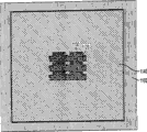
Should also be noted that in original mask figure shown in Figure 8, to have geometric distribution heterogeneous, and the effective coverage figure only is 9% (just only account for the zone that overall appointment covers unconcerned zone 9% and have the printed feature of wanting).And after respectively original figure being decomposed into vertical and level mask figure and after being applied in the OPC technology shown in Fig. 9 a and the 9b, the layout that obtains at last still has uneven spatial distribution.Yet (Fig. 9 a) effective coverage figure brings up to 13.6% from 9%, brings up to 17.3% for horizontal layout (Fig. 9 b) effective coverage figure from 9% for vertical layout.Therefore, after being decomposed into level and vertical mask graph, remain a great opening zone without any protection, this will be subjected to the hot spot of exposure system.
Figure 10 a and 10b have described the result of step 84 and step 83 respectively.Shown in Figure 10 a, the horizontal orientation shielding conductor 72 that can not differentiate is affixed on the elevational plot in open background area (step 84).Similarly, shown in Figure 10 b, the vertical orientation shielding conductor 72 that can not differentiate is affixed on the horizontal figure in open background area (step 83).As mentioned above, the background shielding can not cause the modulation of brightness in X magnetic pole or the irradiation of Y magnetic pole.And, after using shielding conductor, can (Figure 10 a), can bring up to 35% (Figure 10 b) from 17.3% from 13.6% bringing up to 30% for the effective coverage figure of horizontal layout for the effective coverage figure of vertical layout.Form shown in Figure 11 has been summed up the growth at the effective coverage figure of the various figures shown in Fig. 8-10.It should be noted that the effective coverage figure of higher percentage has blocked more stray light with regard to the processing that means SGB, thereby reduced more hot spot negative effect.
Figure 12 a has described vertical with the use shown in the 10b at Figure 10 a respectively and aerial image Simulation result level mask with 12b, and they have comprised the SGB shielding in the double dipole exposure technology.Shown in Figure 12 a, with the result standard gray scale of the various part correlations of gained brightness be following content: zone 1120, corresponding main feature shielding area, 0%; Zone 1130, corresponding 25% circuit structure part; Zone 1140, the corresponding zone that is covered by the SGB shielding, 50%; Zone 1160, corresponding zone, 100% without any shielding.As implied above, the zone 1140 that is covered by horizontal SGB shielding has a relative brightness grade that is lower than the zone (1160) 50% that does not have shielding.Therefore, the quantity of SGB shielding can effectively minimizing bias light.Figure 12 b has described the similar results for level mask.
Figure 13 a and 13b have described in the result who is included in the complete resist model that the mask graph of zone in 30 partly simulate shown in Fig. 2 a and the 2b.The SGB line that is applied on vertical and the level mask figure has the pitch of 120nm and the width of 40nm.Shown in Figure 13 a and 13b, append to the setting that shielding conductor 72 on the mask graph can not hinder scattering strip, can not cause printing to scattering strip yet.
The validity of SGB of the present invention can be verified by following method, promptly adopt the ASML PAS5500/1100ArF that uses identical resist technology, 0.75NA stepping-scanning system, exposing one group has SGB and another group does not have two groups of dipole reticles of SGB.Being configured to of double dipole exposure: NA=0.75, the opening of 35 degree, σ inner=0.64, σ outer=0.89.The pitch that this illumination is provided with for 170nm is optimized configuration, pitch=λ/(2 σ cNA), with maximize the 0th and+lap of/-1 time diffraction order is so that maximization depth of focus (DOF), wherein σ c=(σ inner+ σ outer)/2.Because stray light has bigger influence to intensive pitch, this checking just concentrates on the 70nm target CD with 170nm pitch.Figure 14 a and 14b have described the target CD that the reticle (DS5B) that has the higher SGB of needs can not reach 70nm, and have 20% raising than the DS5 reticle that does not have SGB on exposure latitude.These experimental results show uses SGB can effectively reduce stray light, and improves picture contrast and enhanced process tolerance.
In order to confirm that SGB is the process tolerance that how to influence efficient apparatus, will be applied in SGB in the manufacturing of sram cell.Figure 15 a-15c has narrated these results.Carrying out CD on the NMOS of 65nm grid measures.The measuring position of rectangle 150 flag F EM CD among Figure 15 b.Shown in Figure 15 c, the SRAM that handled with SGB demonstrates the exposure latitude more than the SRAM that does not adopt SGB to handle about 20%.Should be noted that resist simulation and SEM resist image are presented at respectively among Figure 15 a and the 15b.
As last test, the test of the disappearance box of Joseph Kirk is modified and is used for double-exposure, to quantize in the quantity of using and do not use the hot spot under the SGB figure situation.The disappearance cartridge module is designed to the box from 0.6um to the 5.0um variable-size.This module is arranged on level and the vertical scale line position accurately.The array of same cartridge is treated to the SGB of 1mm length, and each box 3mm of being separated by places.By using following formula to calculate the percentage of hot spot:
Straylight%=E
0(dose?to?clear)/E
box(dose?to?remove)
Figure 16 has described the result of test.Disappearance box array with SGB has about 1.5% low hot spot (or raising of about 33%) on the whole.Should be noted that hot spot is very sensitive to surrounding environment, particularly in SGB converges to the scope of non-SGB effect.The quantity that hot spot reduces depends on the scope of SGB.A big SGB scope will produce the effect that better reduces hot spot.
It should be noted that in above-mentioned narration the present invention is used to produce vertically and the said method of level mask is typically to adopt CAD system in conjunction with the MaskWeaver that sells such as ASML MaskTools
TMFinish Deng mask generation software.This CAD system and mask design software can design the program that comprises processing procedure of the present invention easily.
Figure 17 has schematically narrated a kind of lithographic projection apparatus that is fit to be applied to the designed mask of the present invention.This equipment comprises:
A radiating system Ex, IL is used to supply the projected light beam PB of radiation.Radiating system also comprises radiation source LA in this particular case;
First object table (mask platform) MT who has been equipped with the mask clamper, it is used for fixing mask MA (for example reticle), and is connected to first positioner, is used for accurate localization about project PL mask;
Second object table (chip bench) WT who has been equipped with substrate holder, it is used for fixing substrate W (for example silicon wafer of underseal), and is connected to second positioner, is used for accurate localization about project PL substrate;
An optical projection system (" lens ") PL (for example optical system of refraction, reflection or a double reverberation and a refract light), it is used for the illuminated portion of the last mask MA of imaging of target portion C (for example comprising one or more matrixs) at substrate W.
Such as here description, this device is transmission-type (just having transmission mask).Yet it also can be a reflection type usually, for example (has reflection mask).Interchangeable, this device can use the patterning apparatus of other type as the selection that mask is used; For example comprise a programmable mirror array or LCD matrix.
Light source LA (for example charging source of mercury lamp, excimer laser or a plasma) produces radiation laser beam.This light beam is sent to illuminator (lighting device) IL, and it can be directly or through after the adjusting device, for example is transferred after through optical beam expander Ex.Luminaire IL can comprise adjusting device AM, is used for being provided with the radiation scope (being called the outside and σ inside of σ usually respectively) of the outside and/or inner luminance distribution of light beam.In addition, it will comprise various other parts usually, such as integrator IN and concentrator CO.Under this mode, uniformity and density distribution that the light beam PB on the bump mask MA will obtain expecting in its section.
It should be noted for Figure 17, light source LA can be in the shell interior (being under the situation of mercury lamp at light source LA usually for example) of lithographic apparatus, but it also can be provided with away from lithographic apparatus, and the radiation laser beam that it produces is sent to (for example under the help of suitable directed eyeglass) in the device; The latter's situation is (for example, based on K under the situation of an excimer laser at light source LA normally
1F, A
1F or F
2Emission laser).Current invention has comprised both of these case.
Light beam PB intercepts the mask MA that is fixed on the mask table MT subsequently.Light beam B is just passing through lens PL through after the mask MA, and wherein lens PL is focused at light beam PB on the target part of substrate W.By means of second positioner (with interfering meter measuring device IF), chip bench WT just can accurately be moved, for example so that locate different target portion C on the path of light beam PB.Similarly, first positioner can be used in accurate localization about the mask MA on the path of light beam PB, for example, flexibly retrieve mask MA from the mask storehouse after, or finishes a scan period.Usually, object table MT, moving of WT will realize that these contents are not described by means of long stroke module (coarse positioning) and short stroke module (fine positioning) in Figure 17.Yet under the situation of using wafer stepper (in contrast to the device of stepping-scanning), mask table MT can only be connected to the short stroke exciter, perhaps can be fixed.
Described device can be used in two different patterns:
In step mode, mask table MT comes down to be maintained fixed, and whole mask images is projected on the target portion C by once (single " flash of light " just).Chip bench WT is shifted x and/or y direction then, so that light beam PB can shine different target portion C;
In scan pattern, except a specific target portion C is not exposed in once glistening, be to adopt identical scheme basically.The substitute is, mask table MT (so-called " scanning direction ", for example y direction) on specific direction moves with a speed v, so that projected light beam PB can be in the enterprising line scanning of mask images; Simultaneously, chip bench WT moves with identical or opposite direction simultaneously with the speed of V=Mv, and wherein M is the magnification ratio (typical, M=1/4 or 1/5) of lens PL.Under this mode, the target portion C that just can expose big relatively, and do not need to take the solution of trading off.
As mentioned above, method of the present invention provides the significant advantage that is better than prior art.For example, the invention provides a kind of effective minimizing technology of hot spot on a large scale, so that be minimized in the hot spot influence in the exposure process.Importantly, technology of the present invention can not hinder the setting of supplemental characteristic, can not cause the printing to supplemental characteristic yet.And method of the present invention can not cause the increase of number of masks during the imaging process.
In addition, also can change accordingly the foregoing description content.For example, though the SGB line shown in Figure 10 a and the 10b is interrupted, it also can be continuous lines or other shape, for example is not limited to square, and circle etc. are as long as the geometric figure of shielding keeps as Figure 18 a the secondary resolution shown in the 18b.This in SGB shielding continuously the use of long line have the additional advantage of the minimizing data capacity relevant with mask.
In another changed, although be not more superior method, the mode that also can adopt the line that will comprise among the SGB to aim at the feature of printing constituted SGB.Yet SGB is in the orientation of high-contrast in such an embodiment, therefore will increase the printability of SGB.
Although the invention discloses several certain embodiments, should be noted that under the situation that does not break away from spirit of the present invention or inner characteristic and can carry out the change of other form the present invention.Therefore the embodiment that proposes of the present invention is used for illustrative effect rather than limitation of the present invention, the invention scope of in appended claims, pointing out, and with claim identical meanings and scope in all changes all should comprise in the present invention.