In solid-state physics and solid-state chemistry, a band gap, also called a bandgap or energy gap, is an energy range in a solid where no electronic states exist. In graphs of the electronic band structure of solids, the band gap refers to the energy difference between the top of the valence band and the bottom of the conduction band in insulators and semiconductors. It is the energy required to promote an electron from the valence band to the conduction band. The resulting conduction-band electron are free to move within the crystal lattice and serve as charge carriers to conduct electric current. It is closely related to the HOMO/LUMO gap in chemistry. If the valence band is completely full and the conduction band is completely empty, then electrons cannot move within the solid because there are no available states. If the electrons are not free to move within the crystal lattice, then there is no generated current due to no net charge carrier mobility. However, if some electrons transfer from the valence band to the conduction band, then current can flow. Therefore, the band gap is a major factor determining the electrical conductivity of a solid. Substances having large band gaps are generally insulators, those with small band gaps are semiconductor, and conductors either have very small band gaps or none, because the valence and conduction bands overlap to form a continuous band.

A polaron is a quasiparticle used in condensed matter physics to understand the interactions between electrons and atoms in a solid material. The polaron concept was proposed by Lev Landau in 1933 and Solomon Pekar in 1946 to describe an electron moving in a dielectric crystal where the atoms displace from their equilibrium positions to effectively screen the charge of an electron, known as a phonon cloud. This lowers the electron mobility and increases the electron's effective mass.
In solid-state physics, the electron mobility characterises how quickly an electron can move through a metal or semiconductor when pulled by an electric field. There is an analogous quantity for holes, called hole mobility. The term carrier mobility refers in general to both electron and hole mobility.

In chemistry, a dangling bond is an unsatisfied valence on an immobilized atom. An atom with a dangling bond is also referred to as an immobilized free radical or an immobilized radical, a reference to its structural and chemical similarity to a free radical.

A protocrystalline phase is a distinct phase occurring during crystal growth, which evolves into a microcrystalline form. The term is typically associated with silicon films in optical applications such as solar cells.
Variable-range hopping is a model used to describe carrier transport in a disordered semiconductor or in amorphous solid by hopping in an extended temperature range. It has a characteristic temperature dependence of

Multi-junction (MJ) solar cells are solar cells with multiple p–n junctions made of different semiconductor materials. Each material's p-n junction will produce electric current in response to different wavelengths of light. The use of multiple semiconducting materials allows the absorbance of a broader range of wavelengths, improving the cell's sunlight to electrical energy conversion efficiency.
In solid-state physics, the Poole–Frenkel effect is a model describing the mechanism of trap-assisted electron transport in an electrical insulator. It is named after Yakov Frenkel, who published on it in 1938, extending the theory previously developed by H. H. Poole.

In semiconductor physics, the band gap of a semiconductor can be of two basic types, a direct band gap or an indirect band gap. The minimal-energy state in the conduction band and the maximal-energy state in the valence band are each characterized by a certain crystal momentum (k-vector) in the Brillouin zone. If the k-vectors are different, the material has an "indirect gap". The band gap is called "direct" if the crystal momentum of electrons and holes is the same in both the conduction band and the valence band; an electron can directly emit a photon. In an "indirect" gap, a photon cannot be emitted because the electron must pass through an intermediate state and transfer momentum to the crystal lattice.
As the devices continue to shrink further into the sub-100 nm range following the trend predicted by Moore’s law, the topic of thermal properties and transport in such nanoscale devices becomes increasingly important. Display of great potential by nanostructures for thermoelectric applications also motivates the studies of thermal transport in such devices. These fields, however, generate two contradictory demands: high thermal conductivity to deal with heating issues in sub-100 nm devices and low thermal conductivity for thermoelectric applications. These issues can be addressed with phonon engineering, once nanoscale thermal behaviors have been studied and understood.

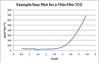
A Tauc plot is used to determine the optical bandgap, or Tauc bandgap, of either disordered or amorphous semiconductors.
A plasmonic-enhanced solar cell, commonly referred to simply as plasmonic solar cell, is a type of solar cell that converts light into electricity with the assistance of plasmons, but where the photovoltaic effect occurs in another material.
In theoretical chemistry, the Buckingham potential is a formula proposed by Richard Buckingham which describes the Pauli exclusion principle and van der Waals energy for the interaction of two atoms that are not directly bonded as a function of the interatomic distance . It is a variety of interatomic potentials.

A phonovoltaic (pV) cell converts vibrational (phonons) energy into a direct current much like the photovoltaic effect in a photovoltaic (PV) cell converts light (photon) into power. That is, it uses a p-n junction to separate the electrons and holes generated as valence electrons absorb optical phonons more energetic than the band gap, and then collects them in the metallic contacts for use in a circuit. The pV cell is an application of heat transfer physics and competes with other thermal energy harvesting devices like the thermoelectric generator.

Amorphous silicon (a-Si) is the non-crystalline form of silicon used for solar cells and thin-film transistors in LCDs.
Charge transport mechanisms are theoretical models that aim to quantitatively describe the electric current flow through a given medium.
Optoelectronic reciprocity relations relate properties of a diode under illumination to the photon emission of the same diode under applied voltage. The relations are useful for interpretation of luminescence based measurements of solar cells and modules and for the analysis of recombination losses in solar cells.

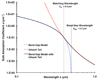
The Urbach tail is an exponential part in the energy spectrum of the absorption coefficient. This tail appears near the optical band edge in amorphous, disordered and crystalline materials.

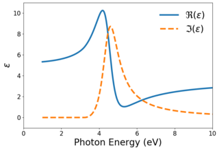
The Tauc–Lorentz model is a mathematical formula for the frequency dependence of the complex-valued relative permittivity, sometimes referred to as the dielectric function. The model has been used to fit the complex refractive index of amorphous semiconductor materials at frequencies greater than their optical band gap. The dispersion relation bears the names of Jan Tauc and Hendrik Lorentz, whose previous works were combined by G. E. Jellison and F. A. Modine to create the model. The model was inspired, in part, by shortcomings of the Forouhi–Bloomer model, which is aphysical due to its incorrect asymptotic behavior and non-Hermitian character. Despite the inspiration, the Tauc–Lorentz model is itself aphysical due to being non-Hermitian and non-analytic in the upper half-plane. Further researchers have modified the model to address these shortcomings.
In statistics, a Kaniadakis distribution is a statistical distribution that emerges from the Kaniadakis statistics. There are several families of Kaniadakis distributions related to different constraints used in the maximization of the Kaniadakis entropy, such as the κ-Exponential distribution, κ-Gaussian distribution, Kaniadakis κ-Gamma distribution and κ-Weibull distribution. The κ-distributions have been applied for modeling a vast phenomenology of experimental statistical distributions in natural or artificial complex systems, such as, in epidemiology, quantum statistics, in astrophysics and cosmology, in geophysics, in economy, in machine learning.


