A synthetic diamond or laboratory-grown diamond (LGD), also called a lab-grown diamond, [1] laboratory-created, man-made, artisan-created, artificial, synthetic, or cultured diamond, is a diamond that is produced in a controlled technological process (in contrast to naturally formed diamond, which is created through geological processes and obtained by mining). Unlike diamond simulants (imitations of diamond made of superficially similar non-diamond materials), synthetic diamonds are composed of the same material as naturally formed diamonds—pure carbon crystallized in an isotropic 3D form—and share identical chemical and physical properties. As of 2023 [update] the heaviest synthetic diamond ever made weighs 30.18 ct (6.0 g), [2] and the heaviest natural diamond ever found weighs 3167 ct (633.4 g).
Numerous claims of diamond synthesis were reported between 1879 and 1928 after an English Chemist named Smithson Tennant demonstrated that diamonds are a form of carbon in 1797; [3] most of these attempts were carefully analyzed but none was confirmed. In the 1940s, systematic research of diamond creation began in the United States, Sweden and the Soviet Union, which culminated in the first reproducible synthesis in 1953. Further research activity yielded the discoveries of high pressure high temperature diamond (HPHT) and CVD diamond, named for their production method (high-pressure high-temperature and chemical vapor deposition, respectively). These two processes still dominate synthetic diamond production. A third method in which nanometer-sized diamond grains are created in a detonation of carbon-containing explosives, known as detonation synthesis, entered the market in the late 1990s. A fourth method, treating graphite with high-power ultrasound, has been demonstrated in the laboratory, but as of 2008 had no commercial application.
The properties of synthetic diamonds depend on the manufacturing process. Some have properties such as hardness, thermal conductivity and electron mobility that are superior to those of most naturally formed diamonds. Synthetic diamond is widely used in abrasives, in cutting and polishing tools and in heat sinks. Electronic applications of synthetic diamond are being developed, including high-power switches at power stations, high-frequency field-effect transistors and light-emitting diodes. Synthetic diamond detectors of ultraviolet (UV) light or high-energy particles are used at high-energy research facilities and are available commercially. Due to its unique combination of thermal and chemical stability, low thermal expansion and high optical transparency in a wide spectral range, synthetic diamond is becoming the most popular material for optical windows in high-power CO
2 lasers and gyrotrons. It is estimated that 98% of industrial-grade diamond demand is supplied with synthetic diamonds. [4]
Both CVD and HPHT diamonds can be cut into gems and various colors can be produced: clear white, yellow, brown, blue, green and orange. The advent of synthetic gems on the market created major concerns in the diamond trading business, as a result of which special spectroscopic devices and techniques have been developed to distinguish synthetic and natural diamonds.
In the early stages of diamond synthesis, the founding figure of modern chemistry, Antoine Lavoisier, played a significant role. His groundbreaking discovery that a diamond's crystal lattice is similar to carbon's crystal structure paved the way for initial attempts to produce diamonds. [5] After it was discovered that diamond was pure carbon in 1797, [6] [7] many attempts were made to convert various cheap forms of carbon into diamond. [8] [a] The earliest successes were reported by James Ballantyne Hannay in 1879 [13] and by Ferdinand Frédéric Henri Moissan in 1893. Their method involved heating charcoal at up to 3,500 °C (6,330 °F) with iron inside a carbon crucible in a furnace. Whereas Hannay used a flame-heated tube, Moissan applied his newly developed electric arc furnace, in which an electric arc was struck between carbon rods inside blocks of lime. [14] The molten iron was then rapidly cooled by immersion in water. The contraction generated by the cooling supposedly produced the high pressure required to transform graphite into diamond. Moissan published his work in a series of articles in the 1890s. [8] [15]
Many other scientists tried to replicate his experiments. Sir William Crookes claimed success in 1909. [16] Otto Ruff claimed in 1917 to have produced diamonds up to 7 mm (0.28 in) in diameter, [17] but later retracted his statement. [18] In 1926, Dr. J. Willard Hershey of McPherson College replicated Moissan's and Ruff's experiments, [19] [20] producing a synthetic diamond. [21] Despite the claims of Moissan, Ruff, and Hershey, other experimenters were unable to reproduce their synthesis. [22] [23]
The most definitive replication attempts were performed by Sir Charles Algernon Parsons. A prominent scientist and engineer known for his invention of the steam turbine, he spent about 40 years (1882–1922) and a considerable part of his fortune trying to reproduce the experiments of Moissan and Hannay, but also adapted processes of his own. [24] Parsons was known for his painstakingly accurate approach and methodical record keeping; all his resulting samples were preserved for further analysis by an independent party. [25] He wrote a number of articles—some of the earliest on HPHT diamond—in which he claimed to have produced small diamonds. [26] However, in 1928, he authorized Dr. C. H. Desch to publish an article [27] in which he stated his belief that no synthetic diamonds (including those of Moissan and others) had been produced up to that date. He suggested that most diamonds that had been produced up to that point were likely synthetic spinel. [22]
The first known (but initially not reported) diamond synthesis was achieved on February 16, 1953, in Stockholm by ASEA (Allmänna Svenska Elektriska Aktiebolaget), Sweden's major electrical equipment manufacturing company. Starting in 1942, ASEA employed a team of five scientists and engineers as part of a top-secret diamond-making project code-named QUINTUS. The team used a bulky split-sphere apparatus designed by Baltzar von Platen and Anders Kämpe. [28] [29] Pressure was maintained within the device at an estimated 8.4 GPa (1,220,000 psi) and a temperature of 2,400 °C (4,350 °F) for an hour. A few small diamonds were produced, but not of gem quality or size.
Due to questions on the patent process and the reasonable belief that no other serious diamond synthesis research occurred globally, the board of ASEA opted against publicity and patent applications. Thus the announcement of the ASEA results occurred shortly after the GE press conference of February 15, 1955. [30]
In 1941, an agreement was made between the General Electric (GE), Norton and Carborundum companies to further develop diamond synthesis. They were able to heat carbon to about 3,000 °C (5,430 °F) under a pressure of 3.5 gigapascals (510,000 psi) for a few seconds. Soon thereafter, the Second World War interrupted the project. It was resumed in 1951 at the Schenectady Laboratories of GE, and a high-pressure diamond group was formed with Francis P. Bundy and H. M. Strong. Tracy Hall and others joined the project later. [28]
The Schenectady group improved on the anvils designed by Percy Bridgman, who received a Nobel Prize in Physics for his work in 1946. Bundy and Strong made the first improvements, then more were made by Hall. The GE team used tungsten carbide anvils within a hydraulic press to squeeze the carbonaceous sample held in a catlinite container, the finished grit being squeezed out of the container into a gasket. The team recorded diamond synthesis on one occasion, but the experiment could not be reproduced because of uncertain synthesis conditions, [31] and the diamond was later shown to have been a natural diamond used as a seed. [32]
Hall achieved the first commercially successful synthesis of diamond on December 16, 1954, and this was announced on February 15, 1955. His breakthrough came when he used a press with a hardened steel toroidal "belt" strained to its elastic limit wrapped around the sample, producing pressures above 10 GPa (1,500,000 psi) and temperatures above 2,000 °C (3,630 °F). [33] The press used a pyrophyllite container in which graphite was dissolved within molten nickel, cobalt or iron. Those metals acted as a "solvent-catalyst", which both dissolved carbon and accelerated its conversion into diamond. The largest diamond he produced was 0.15 mm (0.0059 in) across; it was too small and visually imperfect for jewelry, but usable in industrial abrasives. Hall's co-workers were able to replicate his work, and the discovery was published in the major journal Nature. [34] [35] He was the first person to grow a synthetic diamond with a reproducible, verifiable and well-documented process. He left GE in 1955, and three years later developed a new apparatus for the synthesis of diamond—a tetrahedral press with four anvils—to avoid violating a U.S. Department of Commerce secrecy order on the GE patent applications. [32] [36]
Synthetic gem-quality diamond crystals were first produced in 1970 by GE, then reported in 1971. The first successes used a pyrophyllite tube seeded at each end with thin pieces of diamond. The graphite feed material was placed in the center and the metal solvent (nickel) between the graphite and the seeds. The container was heated and the pressure was raised to about 5.5 GPa (800,000 psi). The crystals grow as they flow from the center to the ends of the tube, and extending the length of the process produces larger crystals. Initially, a week-long growth process produced gem-quality stones of around 5 mm (0.20 in) (1 carat or 0.2 g), and the process conditions had to be as stable as possible. The graphite feed was soon replaced by diamond grit because that allowed much better control of the shape of the final crystal. [35] [37]
The first gem-quality stones were always yellow to brown in color because of contamination with nitrogen. Inclusions were common, especially "plate-like" ones from the nickel. Removing all nitrogen from the process by adding aluminum or titanium produced colorless "white" stones, and removing the nitrogen and adding boron produced blue ones. [38] Removing nitrogen also slowed the growth process and reduced the crystalline quality, so the process was normally run with nitrogen present.
Although the GE stones and natural diamonds were chemically identical, their physical properties were not the same. The colorless stones produced strong fluorescence and phosphorescence under short-wavelength ultraviolet light, but were inert under long-wave UV. Among natural diamonds, only the rarer blue gems exhibit these properties. Unlike natural diamonds, all the GE stones showed strong yellow fluorescence under X-rays. [39] The De Beers Diamond Research Laboratory has grown stones of up to 25 carats (5.0 g) for research purposes. Stable HPHT conditions were kept for six weeks to grow high-quality diamonds of this size. For economic reasons, the growth of most synthetic diamonds is terminated when they reach a mass of 1 carat (200 mg) to 1.5 carats (300 mg). [40]
In the 1950s, research started in the Soviet Union and the US on the growth of diamond by pyrolysis of hydrocarbon gases at the relatively low temperature of 800 °C (1,470 °F). This low-pressure process is known as chemical vapor deposition (CVD). William G. Eversole reportedly achieved vapor deposition of diamond over diamond substrate in 1953, but it was not reported until 1962. [41] [42] Diamond film deposition was independently reproduced by Angus and coworkers in 1968 [43] and by Deryagin and Fedoseev in 1970. [44] [45] Whereas Eversole and Angus used large, expensive, single-crystal diamonds as substrates, Deryagin and Fedoseev succeeded in making diamond films on non-diamond materials (silicon and metals), which led to massive research on inexpensive diamond coatings in the 1980s. [46]
From 2013, reports emerged of a rise in undisclosed synthetic melee diamonds (small round diamonds typically used to frame a central diamond or embellish a band) [47] being found in set jewelry and within diamond parcels sold in the trade. [48] Due to the relatively low cost of diamond melee, as well as relative lack of universal knowledge for identifying large quantities of melee efficiently, [49] not all dealers have made an effort to test diamond melee to correctly identify whether it is of natural or synthetic origin. However, international laboratories are now beginning to tackle the issue head-on, with significant improvements in synthetic melee identification being made. [50]
There are several methods used to produce synthetic diamonds. The original method uses high pressure and high temperature (HPHT) and is still widely used because of its relatively low cost. The process involves large presses that can weigh hundreds of tons to produce a pressure of 5 GPa (730,000 psi) at 1,500 °C (2,730 °F). The second method, using chemical vapor deposition (CVD), creates a carbon plasma over a substrate onto which the carbon atoms deposit to form diamond. Other methods include explosive formation (forming detonation nanodiamonds) and sonication of graphite solutions. [51] [52] [53]
In the HPHT method, there are three main press designs used to supply the pressure and temperature necessary to produce synthetic diamond: the belt press, the cubic press and the split-sphere (BARS) press. Diamond seeds are placed at the bottom of the press. The internal part of the press is heated above 1,400 °C (2,550 °F) and melts the solvent metal. The molten metal dissolves the high purity carbon source, which is then transported to the small diamond seeds and precipitates, forming a large synthetic diamond. [54]
The original GE invention by Tracy Hall uses the belt press wherein the upper and lower anvils supply the pressure load to a cylindrical inner cell. This internal pressure is confined radially by a belt of pre-stressed steel bands. The anvils also serve as electrodes providing electric current to the compressed cell. A variation of the belt press uses hydraulic pressure, rather than steel belts, to confine the internal pressure. [54] Belt presses are still used today, but they are built on a much larger scale than those of the original design. [55]
The second type of press design is the cubic press. A cubic press has six anvils which provide pressure simultaneously onto all faces of a cube-shaped volume. [56] The first multi-anvil press design was a tetrahedral press, using four anvils to converge upon a tetrahedron-shaped volume. [57] The cubic press was created shortly thereafter to increase the volume to which pressure could be applied. A cubic press is typically smaller than a belt press and can more rapidly achieve the pressure and temperature necessary to create synthetic diamond. However, cubic presses cannot be easily scaled up to larger volumes: the pressurized volume can be increased by using larger anvils, but this also increases the amount of force needed on the anvils to achieve the same pressure. An alternative is to decrease the surface area to volume ratio of the pressurized volume, by using more anvils to converge upon a higher-order platonic solid, such as a dodecahedron. However, such a press would be complex and difficult to manufacture. [56]
The BARS apparatus is claimed to be the most compact, efficient, and economical of all the diamond-producing presses. In the center of a BARS device, there is a ceramic cylindrical "synthesis capsule" of about 2 cm3 (0.12 cu in) in size. The cell is placed into a cube of pressure-transmitting material, such as pyrophyllite ceramics, which is pressed by inner anvils made from cemented carbide (e.g., tungsten carbide or VK10 hard alloy). [58] The outer octahedral cavity is pressed by 8 steel outer anvils. After mounting, the whole assembly is locked in a disc-type barrel with a diameter about 1 m (3 ft 3 in). The barrel is filled with oil, which pressurizes upon heating, and the oil pressure is transferred to the central cell. The synthesis capsule is heated up by a coaxial graphite heater, and the temperature is measured with a thermocouple. [59]
Chemical vapor deposition is a method by which diamond can be grown from a hydrocarbon gas mixture. Since the early 1980s, this method has been the subject of intensive worldwide research. Whereas the mass production of high-quality diamond crystals make the HPHT process the more suitable choice for industrial applications, the flexibility and simplicity of CVD setups explain the popularity of CVD growth in laboratory research. The advantages of CVD diamond growth include the ability to grow diamond over large areas and on various substrates, and the fine control over the chemical impurities and thus properties of the diamond produced. Unlike HPHT, CVD process does not require high pressures, as the growth typically occurs at pressures under 27 kPa (3.9 psi). [51] [60]
The CVD growth involves substrate preparation, feeding varying amounts of gases into a chamber and energizing them. The substrate preparation includes choosing an appropriate material and its crystallographic orientation; cleaning it, often with a diamond powder to abrade a non-diamond substrate; and optimizing the substrate temperature (about 800 °C (1,470 °F)) during the growth through a series of test runs. Moreover, optimizing the gas mixture composition and flow rates is paramount to ensure uniform and high-quality diamond growth. The gases always include a carbon source, typically methane, and hydrogen with a typical ratio of 1:99. Hydrogen is essential because it selectively etches off non-diamond carbon. The gases are ionized into chemically active radicals in the growth chamber using microwave power, a hot filament, an arc discharge, a welding torch, a laser, an electron beam, or other means.
During the growth, the chamber materials are etched off by the plasma and can incorporate into the growing diamond. In particular, CVD diamond is often contaminated by silicon originating from the silica windows of the growth chamber or from the silicon substrate. [61] Therefore, silica windows are either avoided or moved away from the substrate. Boron-containing species in the chamber, even at very low trace levels, also make it unsuitable for the growth of pure diamond. [51] [60] [62]
Diamond nanocrystals (5 nm (2.0×10⁻⁷ in) in diameter) can be formed by detonating certain carbon-containing explosives in a metal chamber. These are called "detonation nanodiamonds". During the explosion, the pressure and temperature in the chamber become high enough to convert the carbon of the explosives into diamond. Being immersed in water, the chamber cools rapidly after the explosion, suppressing conversion of newly produced diamond into more stable graphite. [63] In a variation of this technique, a metal tube filled with graphite powder is placed in the detonation chamber. The explosion heats and compresses the graphite to an extent sufficient for its conversion into diamond. [64] The product is always rich in graphite and other non-diamond carbon forms, and requires prolonged boiling in hot nitric acid (about 1 day at 250 °C (482 °F)) to dissolve them. [52] The recovered nanodiamond powder is used primarily in polishing applications. It is mainly produced in China, Russia and Belarus, and started reaching the market in bulk quantities by the early 2000s. [65]
Micron-sized diamond crystals can be synthesized from a suspension of graphite in organic liquid at atmospheric pressure and room temperature using ultrasonic cavitation. The diamond yield is about 10% of the initial graphite weight. The estimated cost of diamond produced by this method is comparable to that of the HPHT method but the crystalline perfection of the product is significantly worse for the ultrasonic synthesis. This technique requires relatively simple equipment and procedures, and has been reported by two research groups, but had no industrial use as of 2008. Numerous process parameters, such as preparation of the initial graphite powder, the choice of ultrasonic power, synthesis time and the solvent, were not optimized, leaving a window for potential improvement of the efficiency and reduction of the cost of the ultrasonic synthesis. [53] [66]
In 2024, scientists announced a method that utilizes injecting methane and hydrogen gases onto a liquid metal alloy of gallium, iron, nickel and silicon (77.25/11.00/11.00/0.25 ratio) at approximately 1,025 °C to crystallize diamond at 1 atmosphere of pressure. The crystallization is a ‘seedless’ process, which further separates it from conventional high-pressure and high-temperature or chemical vapor deposition methods. Injection of methane and hydrogen results in a diamond nucleus after around 15 minutes and eventually a continuous diamond film after around 150 minutes. [67] [68]
Traditionally, the absence of crystal flaws is considered to be the most important quality of a diamond. Purity and high crystalline perfection make diamonds transparent and clear, whereas its hardness, optical dispersion (luster), and chemical stability (combined with marketing), make it a popular gemstone. High thermal conductivity is also important for technical applications. Whereas high optical dispersion is an intrinsic property of all diamonds, their other properties vary depending on how the diamond was created. [69]
Diamond can be one single, continuous crystal or it can be made up of many smaller crystals (polycrystal). Large, clear and transparent single-crystal diamonds are typically used as gemstones. Polycrystalline diamond (PCD) consists of numerous small grains, which are easily seen by the naked eye through strong light absorption and scattering; it is unsuitable for gems and is used for industrial applications such as mining and cutting tools. Polycrystalline diamond is often described by the average size (or grain size) of the crystals that make it up. Grain sizes range from nanometers to hundreds of micrometers, usually referred to as "nanocrystalline" and "microcrystalline" diamond, respectively. [70]
The hardness of diamond is 10 on the Mohs scale of mineral hardness, the hardest known material on this scale. Diamond is also the hardest known natural material for its resistance to indentation. [71] The hardness of synthetic diamond depends on its purity, crystalline perfection and orientation: hardness is higher for flawless, pure crystals oriented to the [111] direction (along the longest diagonal of the cubic diamond lattice). [72] Nanocrystalline diamond produced through CVD diamond growth can have a hardness ranging from 30% to 75% of that of single crystal diamond, and the hardness can be controlled for specific applications. Some synthetic single-crystal diamonds and HPHT nanocrystalline diamonds (see hyperdiamond) are harder than any known natural diamond. [71] [73] [74]
Every diamond contains atoms other than carbon in concentrations detectable by analytical techniques. Those atoms can aggregate into macroscopic phases called inclusions. Impurities are generally avoided, but can be introduced intentionally as a way to control certain properties of the diamond. Growth processes of synthetic diamond, using solvent-catalysts, generally lead to formation of a number of impurity-related complex centers, involving transition metal atoms (such as nickel, cobalt or iron), which affect the electronic properties of the material. [75] [76]
For instance, pure diamond is an electrical insulator, but diamond with boron added is an electrical conductor (and, in some cases, a superconductor), [77] allowing it to be used in electronic applications. Nitrogen impurities hinder movement of lattice dislocations (defects within the crystal structure) and put the lattice under compressive stress, thereby increasing hardness and toughness. [78]
The thermal conductivity of CVD diamond ranges from tens of W/m2K to more than 2000 W/m2K, depending on the defects, grain boundary structures. [79] As the growth of diamond in CVD, the grains grow with the film thickness, leading to a gradient thermal conductivity along the film thickness direction. [79]
Unlike most electrical insulators, pure diamond is an excellent conductor of heat because of the strong covalent bonding within the crystal. The thermal conductivity of pure diamond is the highest of any known solid. Single crystals of synthetic diamond enriched in 12
C
(99.9%), isotopically pure diamond, have the highest thermal conductivity of any material, 30 W/cm·K at room temperature, 7.5 times higher than that of copper. Natural diamond's conductivity is reduced by 1.1% by the 13
C
naturally present, which acts as an inhomogeneity in the lattice. [80]
Diamond's thermal conductivity is made use of by jewelers and gemologists who may employ an electronic thermal probe to separate diamonds from their imitations. These probes consist of a pair of battery-powered thermistors mounted in a fine copper tip. One thermistor functions as a heating device while the other measures the temperature of the copper tip: if the stone being tested is a diamond, it will conduct the tip's thermal energy rapidly enough to produce a measurable temperature drop. This test takes about 2–3 seconds. [81]
Most industrial applications of synthetic diamond have long been associated with their hardness; this property makes diamond the ideal material for machine tools and cutting tools. As the hardest known naturally occurring material, diamond can be used to polish, cut, or wear away any material, including other diamonds. Common industrial applications of this ability include diamond-tipped drill bits and saws, and the use of diamond powder as an abrasive. [82] These are by far the largest industrial applications of synthetic diamond. While natural diamond is also used for these purposes, synthetic HPHT diamond is more popular, mostly because of better reproducibility of its mechanical properties. Diamond is not suitable for machining ferrous alloys at high speeds, as carbon is soluble in iron at the high temperatures created by high-speed machining, leading to greatly increased wear on diamond tools compared to alternatives. [83]
The usual form of diamond in cutting tools is micron-sized grains dispersed in a metal matrix (usually cobalt) sintered onto the tool. This is typically referred to in industry as polycrystalline diamond (PCD). PCD-tipped tools can be found in mining and cutting applications. For the past fifteen years, work has been done to coat metallic tools with CVD diamond, and though the work shows promise, it has not significantly replaced traditional PCD tools. [84]
Most materials with high thermal conductivity are also electrically conductive, such as metals. In contrast, pure synthetic diamond has high thermal conductivity, but negligible electrical conductivity. This combination is invaluable for electronics where diamond is used as a heat spreader for high-power laser diodes, laser arrays and high-power transistors. Efficient heat dissipation prolongs the lifetime of those electronic devices, and the devices' high replacement costs justify the use of efficient, though relatively expensive, diamond heat sinks. [85] In semiconductor technology, synthetic diamond heat spreaders prevent silicon and other semiconducting devices from overheating. [86]
Diamond is hard, chemically inert, and has high thermal conductivity and a low coefficient of thermal expansion. These properties make diamond superior to any other existing window material used for transmitting infrared and microwave radiation. Therefore, synthetic diamond is starting to replace zinc selenide as the output window of high-power CO2 lasers [87] and gyrotrons. Those synthetic polycrystalline diamond windows are shaped as disks of large diameters (about 10 cm for gyrotrons) and small thicknesses (to reduce absorption) and can only be produced with the CVD technique. [88] [89] Single crystal slabs of dimensions of length up to approximately 10 mm are becoming increasingly important in several areas of optics including heatspreaders inside laser cavities, diffractive optics and as the optical gain medium in Raman lasers. [90] Recent advances in the HPHT and CVD synthesis techniques have improved the purity and crystallographic structure perfection of single-crystalline diamond enough to replace silicon as a diffraction grating and window material in high-power radiation sources, such as synchrotrons. [91] [92] Both the CVD and HPHT processes are also used to create designer optically transparent diamond anvils as a tool for measuring electric and magnetic properties of materials at ultra high pressures using a diamond anvil cell. [93]
Synthetic diamond has potential uses as a semiconductor, [94] because it can be doped with impurities like boron and phosphorus. Since these elements contain one more or one fewer valence electron than carbon, they turn synthetic diamond into p-type or n-type semiconductor. Making a p–n junction by sequential doping of synthetic diamond with boron and phosphorus produces light-emitting diodes (LEDs) producing UV light of 235 nm. [95] Another useful property of synthetic diamond for electronics is high carrier mobility, which reaches 4500 cm2/(V·s) for electrons in single-crystal CVD diamond. [96] High mobility is favorable for high-frequency operation and field-effect transistors made from diamond have already demonstrated promising high-frequency performance above 50 GHz. [97] [98] The wide band gap of diamond (5.5 eV) gives it excellent dielectric properties. Combined with the high mechanical stability of diamond, those properties are being used in prototype high-power switches for power stations. [99]
Synthetic diamond transistors have been produced in the laboratory. They remain functional at much higher temperatures than silicon devices, and are resistant to chemical and radiation damage. While no diamond transistors have yet been successfully integrated into commercial electronics, they are promising for use in exceptionally high-power situations and hostile non-oxidizing environments. [100] [101]
Synthetic diamond is already used as radiation detection device. It is radiation hard and has a wide bandgap of 5.5 eV (at room temperature). Diamond is also distinguished from most other semiconductors by the lack of a stable native oxide. This makes it difficult to fabricate surface MOS devices, but it does create the potential for UV radiation to gain access to the active semiconductor without absorption in a surface layer. Because of these properties, it is employed in applications such as the BaBar detector at the Stanford Linear Accelerator [102] and BOLD (Blind to the Optical Light Detectors for VUV solar observations). [103] [104] A diamond VUV detector recently was used in the European LYRA program.
Conductive CVD diamond is a useful electrode under many circumstances. [105] Photochemical methods have been developed for covalently linking DNA to the surface of polycrystalline diamond films produced through CVD. Such DNA-modified films can be used for detecting various biomolecules, which would interact with DNA thereby changing electrical conductivity of the diamond film. [106] In addition, diamonds can be used to detect redox reactions that cannot ordinarily be studied and in some cases degrade redox-reactive organic contaminants in water supplies. Because diamond is mechanically and chemically stable, it can be used as an electrode under conditions that would destroy traditional materials. As an electrode, synthetic diamond can be used in waste water treatment of organic effluents [107] and the production of strong oxidants. [108]
Synthetic diamonds for use as gemstones are grown by HPHT [40] or CVD [109] methods, and represented approximately 2% of the gem-quality diamond market as of 2013. [110] However, there are indications that the market share of synthetic jewelry-quality diamonds may grow as advances in technology allow for larger higher-quality synthetic production on a more economical scale. [111] Indeed, by 2023, synthetic diamonds' share had increased to 17% of the overall diamond market. [112] They are available in yellow, pink, green, orange, blue and, to a lesser extent, colorless (or white). The yellow comes from nitrogen impurities in the manufacturing process, while the blue comes from boron. [38] Other colors, such as pink or green, are achievable after synthesis using irradiation. [113] [114] Several companies also offer memorial diamonds grown using cremated remains. [115]
Gem-quality diamonds grown in a lab can be chemically, physically, and optically identical to naturally occurring ones. The mined diamond industry has undertaken legal, marketing, and distribution countermeasures to try to protect its market from the emerging presence of synthetic diamonds. [116] [117] Synthetic diamonds can be distinguished by spectroscopy in the infrared, ultraviolet, or X-ray wavelengths. The DiamondView tester from De Beers uses UV fluorescence to detect trace impurities of nitrogen, nickel, or other metals in HPHT or CVD diamonds. [118]
At least one maker of laboratory-grown diamonds has made public statements about being "committed to disclosure" of the nature of its diamonds, and laser-inscribed serial numbers on all of its gemstones. [109] The company web site shows an example of the lettering of one of its laser inscriptions, which includes both the words "Gemesis created" and the serial number prefix "LG" (laboratory grown). [119]
In May 2015, a record was set for an HPHT colorless diamond at 10.02 carats. The faceted jewel was cut from a 32.2-carat stone that was grown in about 300 hours. [120] By 2022, gem-quality diamonds of 16–20 carats were being produced. [121]
Traditional diamond mining has led to human rights abuses in Africa and other diamond mining countries. The 2006 Hollywood movie Blood Diamond helped to publicize the problem. Consumer demand for synthetic diamonds has been increasing, albeit from a small base, as customers look for ethically sound and cheaper stones. [122]
Apart from the ethical aspect, three key environmental factors play a central role in the ecological comparison of laboratory diamonds and mine diamonds:
According to a Gem & Jewellery Export Promotional Council report, synthetic diamonds accounted for 0.28% of diamonds produced for use as gemstones in 2014. [132] In April 2022, CNN Business [133] reported that engagement rings featuring a synthetic or a lab grown diamond jumped 63% compared to previous year, while the number of engagement rings sold with a natural diamond declined 25% in the same period.
Around 2016, the price of synthetic diamond gemstones (e.g., 1-carat stones) began dropping "precipitously" by roughly 30% in one year, becoming clearly lower than that of mined diamonds. [134] As of 2017, synthetic diamonds sold as jewelry were typically selling for 15–20% less than natural equivalents; the relative price was expected to decline further as production economics improve. [135]
In May 2018, De Beers announced that it would introduce a new jewelry brand called "Lightbox" that features synthetic diamonds. [136]
In July 2018, the U.S. Federal Trade Commission approved a substantial revision to its Jewelry Guides, with changes that impose new rules on how the trade can describe diamonds and diamond simulants. [137] The revised guides were substantially contrary to what had been advocated in 2016 by De Beers. [136] [138] [139] The new guidelines remove the word "natural" from the definition of "diamond", thus including lab-grown diamonds within the scope of the definition of "diamond". The revised guide further states that "If a marketer uses 'synthetic' to imply that a competitor's lab-grown diamond is not an actual diamond, ... this would be deceptive." [140] [138] In July 2019, the third party diamond certification lab GIA (Gemological Institute of America) dropped the word 'synthetic' from its certification process and report for lab-grown diamonds, according to the FTC revision. [141]
Boron nitride is a thermally and chemically resistant refractory compound of boron and nitrogen with the chemical formula BN. It exists in various crystalline forms that are isoelectronic to a similarly structured carbon lattice. The hexagonal form corresponding to graphite is the most stable and soft among BN polymorphs, and is therefore used as a lubricant and an additive to cosmetic products. The cubic variety analogous to diamond is called c-BN; it is softer than diamond, but its thermal and chemical stability is superior. The rare wurtzite BN modification is similar to lonsdaleite but slightly softer than the cubic form.
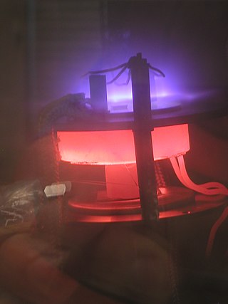
Chemical vapor deposition (CVD) is a vacuum deposition method used to produce high-quality, and high-performance, solid materials. The process is often used in the semiconductor industry to produce thin films.
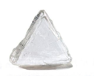
Diamond is a solid form of the element carbon with its atoms arranged in a crystal structure called diamond cubic. Diamond as a form of carbon is tasteless, odourless, strong, brittle solid, colourless in pure form, a poor conductor of electricity, and insoluble in water. Another solid form of carbon known as graphite is the chemically stable form of carbon at room temperature and pressure, but diamond is metastable and converts to it at a negligible rate under those conditions. Diamond has the highest hardness and thermal conductivity of any natural material, properties that are used in major industrial applications such as cutting and polishing tools. They are also the reason that diamond anvil cells can subject materials to pressures found deep in the Earth.
Silicon carbide (SiC), also known as carborundum, is a hard chemical compound containing silicon and carbon. A wide bandgap semiconductor, it occurs in nature as the extremely rare mineral moissanite, but has been mass-produced as a powder and crystal since 1893 for use as an abrasive. Grains of silicon carbide can be bonded together by sintering to form very hard ceramics that are widely used in applications requiring high endurance, such as car brakes, car clutches and ceramic plates in bulletproof vests. Large single crystals of silicon carbide can be grown by the Lely method and they can be cut into gems known as synthetic moissanite.
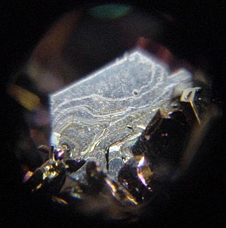
Moissanite is naturally occurring silicon carbide and its various crystalline polymorphs. It has the chemical formula SiC and is a rare mineral, discovered by the French chemist Henri Moissan in 1893. Silicon carbide or moissanite is useful for commercial and industrial applications due to its hardness, optical properties and thermal conductivity.
Carbon is capable of forming many allotropes due to its valency (tetravalent). Well-known forms of carbon include diamond and graphite. In recent decades, many more allotropes have been discovered and researched, including ball shapes such as buckminsterfullerene and sheets such as graphene. Larger-scale structures of carbon include nanotubes, nanobuds and nanoribbons. Other unusual forms of carbon exist at very high temperatures or extreme pressures. Around 500 hypothetical 3‑periodic allotropes of carbon are known at the present time, according to the Samara Carbon Allotrope Database (SACADA).
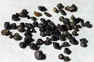
Strontium titanate is an oxide of strontium and titanium with the chemical formula SrTiO3. At room temperature, it is a centrosymmetric paraelectric material with a perovskite structure. At low temperatures it approaches a ferroelectric phase transition with a very large dielectric constant ~104 but remains paraelectric down to the lowest temperatures measured as a result of quantum fluctuations, making it a quantum paraelectric. It was long thought to be a wholly artificial material, until 1982 when its natural counterpart—discovered in Siberia and named tausonite—was recognised by the IMA. Tausonite remains an extremely rare mineral in nature, occurring as very tiny crystals. Its most important application has been in its synthesized form wherein it is occasionally encountered as a diamond simulant, in precision optics, in varistors, and in advanced ceramics.
A superhard material is a material with a hardness value exceeding 40 gigapascals (GPa) when measured by the Vickers hardness test. They are virtually incompressible solids with high electron density and high bond covalency. As a result of their unique properties, these materials are of great interest in many industrial areas including, but not limited to, abrasives, polishing and cutting tools, disc brakes, and wear-resistant and protective coatings.
Gemesis Inc. was a privately held company located in New York City. The company grew synthetic diamonds using proprietary technology.
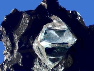
Diamond is the allotrope of carbon in which the carbon atoms are arranged in the specific type of cubic lattice called diamond cubic. It is a crystal that is transparent to opaque and which is generally isotropic. Diamond is the hardest naturally occurring material known. Yet, due to important structural brittleness, bulk diamond's toughness is only fair to good. The precise tensile strength of bulk diamond is little known; however, compressive strength up to 60 GPa has been observed, and it could be as high as 90–100 GPa in the form of micro/nanometer-sized wires or needles, with a corresponding maximum tensile elastic strain in excess of 9%. The anisotropy of diamond hardness is carefully considered during diamond cutting. Diamond has a high refractive index (2.417) and moderate dispersion (0.044) properties that give cut diamonds their brilliance. Scientists classify diamonds into four main types according to the nature of crystallographic defects present. Trace impurities substitutionally replacing carbon atoms in a diamond's crystal structure, and in some cases structural defects, are responsible for the wide range of colors seen in diamond. Most diamonds are electrical insulators and extremely efficient thermal conductors. Unlike many other minerals, the specific gravity of diamond crystals (3.52) has rather small variation from diamond to diamond.
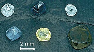
Imperfections in the crystal lattice of diamond are common. Such defects may be the result of lattice irregularities or extrinsic substitutional or interstitial impurities, introduced during or after the diamond growth. The defects affect the material properties of diamond and determine to which type a diamond is assigned; the most dramatic effects are on the diamond color and electrical conductivity, as explained by the electronic band structure.
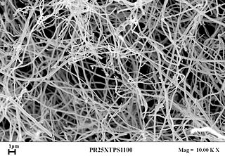
Carbon nanofibers (CNFs), vapor grown carbon fibers (VGCFs), or vapor grown carbon nanofibers (VGCNFs) are cylindrical nanostructures with graphene layers arranged as stacked cones, cups or plates. Carbon nanofibers with graphene layers wrapped into perfect cylinders are called carbon nanotubes.
A multi-anvil press, or anvil press is a type of device related to a machine press that is used to create extraordinarily high pressures within a small volume.
Memorial diamonds are lab-grown diamonds that are promoted as being produced from carbon extracted from human or pet animal hair or cremated remains, cremation diamonds, that are provided to the producer by the customer.
BARS a high-pressure high-temperature apparatus usually used for growing or processing minerals, especially diamond and boron nitride. Typical pressures and temperatures achievable with BARS are 10 GPa (99,000 atm) and 2,500 °C.
Covalent superconductors are superconducting materials where the atoms are linked by covalent bonds. The first such material was boron-doped synthetic diamond grown by the high-pressure high-temperature (HPHT) method. The discovery had no practical importance, but surprised most scientists as superconductivity had not been observed in covalent semiconductors, including diamond and silicon.
WD Lab Grown Diamonds was a manufacturer of synthetic chemical vapor deposition (CVD) diamonds, headquartered in the Washington, D.C. area. Founded in 2008, WD produced lab-grown diamonds for distribution under the brands WD Lab Grown Diamonds and Latitude, in addition to creating diamonds for high-tech Advanced Materials applications. The company formally pivoted and relaunched as WD Advanced Materials, LLC in November 2023.
A rapidly increasing list of graphene production techniques have been developed to enable graphene's use in commercial applications.
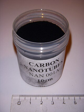
Techniques have been developed to produce carbon nanotubes (CNTs) in sizable quantities, including arc discharge, laser ablation, high-pressure carbon monoxide disproportionation, and chemical vapor deposition (CVD). Most of these processes take place in a vacuum or with process gases. CVD growth of CNTs can occur in a vacuum or at atmospheric pressure. Large quantities of nanotubes can be synthesized by these methods; advances in catalysis and continuous growth are making CNTs more commercially viable.
In materials science, vertically aligned carbon nanotube arrays (VANTAs) are a unique microstructure consisting of carbon nanotubes oriented with their longitudinal axis perpendicular to a substrate surface. These VANTAs effectively preserve and often accentuate the unique anisotropic properties of individual carbon nanotubes and possess a morphology that may be precisely controlled. VANTAs are consequently widely useful in a range of current and potential device applications.