Low Pin Count

Last updated
Low Pin Count
Low Pin Count
Year created1998
Created byIntel
Supersedes Industry Standard Architecture
Superseded by Enhanced Serial Peripheral Interface Bus (2016)
Width in bits4
Speed33 MHz
Style Parallel
Hotplugging interfaceno
External interfaceno
Low Pin Count interface Winbond chip Asus P5PL2 - Winbond W83627EHG-A-93721.jpg
Low Pin Count interface Winbond chip
Trusted Platform Module installed on a motherboard, and using the LPC bus TPM Asus.jpg
Trusted Platform Module installed on a motherboard, and using the LPC bus

The Low Pin Count (LPC) bus is a computer bus used on IBM-compatible personal computers to connect low-bandwidth devices to the CPU, such as the BIOS ROM (BIOS ROM was moved to the Serial Peripheral Interface (SPI) bus in 2006 [1] ), "legacy" I/O devices (integrated into Super I/O, Embedded Controller, CPLD, and/or IPMI chip), and Trusted Platform Module (TPM). [2] "Legacy" I/O devices usually include serial and parallel ports, PS/2 keyboard, PS/2 mouse, and floppy disk controller.

Contents

Most PC motherboards with an LPC bus have either a Platform Controller Hub (PCH) or a southbridge chip, which acts as the host and controls the LPC bus. All other devices connected to the physical wires of the LPC bus are peripherals.

Overview

A diagram showing the LPC bus connecting the southbridge, the flash ROM, and the Super I/O chip Motherboard diagram.svg
A diagram showing the LPC bus connecting the southbridge, the flash ROM, and the Super I/O chip

The LPC bus was introduced by Intel in 1998 as a software-compatible substitute for the Industry Standard Architecture (ISA) bus. It resembles ISA to software, although physically it is quite different. The ISA bus has a 16-bit data bus and a 24-bit address bus that can be used for both 16-bit I/O port addresses and 24-bit memory addresses; both run at speeds up to 8.33  MHz. The LPC bus uses a heavily multiplexed four-bit-wide bus operating at four times the clock speed (33.3 MHz) to transfer addresses and data with similar performance.

LPC's main advantage is that the basic bus requires only seven signals, greatly reducing the number of pins required on peripheral chips. An integrated circuit using LPC will need 30 to 72 fewer pins than its ISA equivalent. This also makes the bus easier to route on crowded modern motherboards. The clock rate was chosen to match that of PCI in order to further ease integration. Also, LPC is intended to be a motherboard-only bus; there is no standardized connector in common use, though Intel defines one for use for debug modules. [3] A small number of LPC peripheral daughterboards are available, with pinouts proprietary to the motherboard vendor: Trusted Platform Modules (TPMs), [2] POST cards for displaying BIOS diagnostic codes, [4] and ISA-compatible serial port peripherals for industrial use. [5] Device discovery is not supported; since only motherboard devices or specific models of TPM are connected, the host firmware (BIOS, UEFI) image will include a static description of any devices and their I/O addresses expected to be present on a particular motherboard.

Signals

LPC control signals are active-low, as indicated by the "#" symbol in their names. Signals are divided into three categories:

The LPC specification defines seven mandatory signals required for bidirectional data transfer:

There are six additional signals defined, which are optional for LPC devices that do not require their functionality, but support for the first two is mandatory for the host:

Timing and performance

The LPC bus derives its electrical conventions from those of conventional PCI. In particular, it shares the restriction that two idle cycles are required to "turn around" any bus signal so that a different device is "speaking". In the first, the bus is actively driven high. In the second, the bus is undriven and held high by the pull-up resistors. A new device may begin sending data over the bus on the third cycle. LPC operations spend a large fraction of their time performing such turn-arounds.

As mentioned, the LPC bus is designed to have performance similar to the ISA bus. The exact data transfer rates depend on the type of bus access (I/O, memory, DMA, firmware) performed and by the speed of the host and the LPC device. All bus cycles spend a majority of their time in overhead rather than data transfer—except the 16- and 128-byte firmware read cycles, which have 17 cycles of overhead but 32 and 256 cycles (respectively) of data transfer, achieving throughputs of 10.88 and 15.63 MB/s. [7] The next fastest bus cycle defined in the standard, the 32-bit ISA-style DMA write cycle, spends only 8 of 20 total clock cycles transferring data (the other 12 cycles are overhead), achieving up to 6.67 MB/s. [7]

One of the slowest bus cycles is a simple memory read or write, where only 2 of the 17 clock cycles (plus any wait states imposed by the device) transfer data, for a transfer rate of 1.96 MB/s.

Transaction structure

LPC transactions begin on a low-to-high transition of LFRAME#. While LFRAME# is low, the host places a 4-bit START code on the LAD lines. The code sent on the last cycle before LFRAME# transitions high defines the following bus transaction.

Normally, the host only holds LFRAME# low for a single clock cycle, for efficiency. An exception is the abort transaction, which may begin even in the middle of another operation. The host pulls LFRAME# low for a minimum of four clock cycles, during which any devices must cease to drive the LAD bus. On the fourth cycle, the host drives LAD high (to 1111). Upon the high-to-low transition of LFRAME#, the bus is reset to an idle state.

In almost all other cases, LPC transactions use the following general structure:

DMA transfers differ somewhat. § ISA-compatible DMA may have multiple SYNC and data phases. § Bus master DMA has a bus turnaround immediately following the START code and no final turnaround,

The SYNC phase allows the device to insert wait states in the transaction. There are six possible SYNC values, all with even parity (even Hamming weight). Three of them end the SYNC phase, while the other three cause the host to wait for another SYNC nibble:

Applications

Intel designed the LPC bus so that the system BIOS image could be stored in a single flash memory chip directly connected to the LPC bus. Intel also made it possible to put operating system images and software applications on a single flash memory chip directly connected to the LPC bus, as an alternative to a Parallel ATA port. [8]

A CPLD or FPGA can implement an LPC host or peripheral. [9]

The original Xbox game console has an LPC debug port that can be used to force the Xbox to boot new code. [10] [11]

ISA-compatible operation

All ISA-compatible LPC bus transactions use START code of 0000. [7] During the first cycle with LFRAME# high again, the host drives a "cycle type/direction" (CTDIR) field: two bits indicating the type (I/O, memory, or DMA) and one bit indicating the direction (read from device, or write to device) of the transfer to follow. This is followed by the transfer address field, whose size depends on the type of cycle:

ISA-compatible reads and writes

Memory and I/O accesses are allowed as single-byte accesses only, and operate as described in § Transactoin structure:: address, data from host if write, turnaround, SYNC, data from device if read.

If the host attempts a transfer to an unused address, no device will drive the SYNC cycles and the host will see 1111 on the LAD bus. After seeing three cycles of 1111 (two cycles are allowed, in addition to the two turn-around cycles, for a slow device to decode the address and begin driving SYNC patterns), the host will abort the operation.

ISA-compatible DMA

The Platform Controller Hub (PCH) chip or the southbridge chip acts as the host and controls the LPC bus. It also acts as the central DMA controller for devices on that bus if the memory controller is in the chipset. In CPUs that contain their own memory controller(s), the DMA controller is located in the CPU. For compatibility with software originally written for systems with the ISA bus, the DMA controller contains the circuit equivalents of "legacy" onboard peripherals of the IBM PC/AT architecture, such as the two programmable interrupt controllers, the programmable interval timer, and two ISA DMA controllers, which are all involved in "ISA-style DMA".

ISA-compatible DMA uses an Intel 8237-compatible DMA controller on the host, which keeps track of the location and length of the memory buffer, as well as the direction of the transfer. The device simply requests service from a given DMA channel number, and the host performs a DMA access on the LPC bus.

The request is made by a virtual ISA-compatible DMA request (DRQ) line, which is emulated using the device's LDRQ# signal to indicate transitions on the emulated DRQ line. This is done with 6-bit requests on the LDRQ# signal: a 0 start bit, the 3-bit DMA channel number (most significant bit first), one bit of new request level (almost always 1, indicating that a DMA transfer is requested), and a final 1 stop bit. The host responds by performing a DMA cycle at the next available opportunity. DMA cycles are named based on the direction of memory access, so a "read" is a transfer to the LPC device, and a "write" is a transfer from the LPC device.

The "address" consists of 6 bits sent as two nibbles: a 3-bit channel number and 1-bit terminal count indication (the ISA bus's TC pin, or the 8237's EOP# output), followed by a 2-bit transfer size.

By default, DMA channels 03 perform 8-bit transfers, and channels 57 perform 16-bit transfers; but an LPC-specific extension allows 1-, 2-, or 4-byte transfers on any channel. When a multi-byte transfer is performed, each byte has its own SYNC field, as described below.

A normal SYNC "ready" pattern of 0000 (or an error pattern of 1010) also causes a deassertion of the corresponding emulated DMA request signal; the host will stop DMA after the immediately following byte until the device makes another DMA request via the LDRQ# signal. A SYNC pattern of 1001 indicates that the host should consider he device's DMA request still active; the host will continue with any remaining bytes in this transfer or start another transfer, as appropriate, without a separate request via LDRQ#.

For a DMA write, where data is transferred from the device, the SYNC field is followed by the 8 bits of data and another SYNC field, until the host-specified length for this transfer is reached, or the device stops the transfer. A two-cycle turnaround field completes the transaction. For a DMA read, where data is transferred to the device, the SYNC field is followed by a turnaround, and the data—turnaround—sync—turnaround sequence repeats for each byte transferred.

Serialized interrupts

Interrupts are transmitted over a single shared SERIRQ line using the "serialized interrupts for PCI" protocol originally developed for the PCI bus. [6] The host periodically sends interrupt packets, within which each interrupt request is assigned a 1-clock time slot, separated by 2-clock turnaround cycles. The initial synchronization is done by the host. As a simplified example:

The devices can recognize the beginning of the frame because only the host will ever drive the line low for more than one cycle. The host identifies the interrupt by counting the number of clocks cycles: if it sees the SERIRQ line driven low at the eighteenth clock, then IRQ 18/3=6 is asserted.

The number of interrupt slots is system-specific, with 17 being a typical number: 16 ISA-compatible interrupts (IRQ0IRQ15), plus NMI.

After the final interrupt slot, the host appends a "stop" signal consisting of two or three low cycles followed by two turnaround cycles.

In "continuous" mode, the host periodically initiates a new packet. There is also a "quiet" mode in which a device requests a new packet by driving SERIRQ low for one clock cycle. The host then continues driving the line low for the other seven clocks. From this point on, the protocol is the same.

The mode is controlled by the length of the host's stop signal at the end of each packet. If it consists of three clocks of low signal, continuous mode follows and only the host may begin a new packet. If the stop signal consists of two low clocks, quiet mode follows and any device may initiate an interrupt packet.

LPC non-ISA transactions

START field values other than 0000 or 1111 are used to indicate various non-ISA-compatible transfers. [7] The supported transfers are:

START = 1101, 1110: Firmware memory read and write

This allows the firmware (BIOS) to be located outside the usual peripheral address space. These transfers are similar to ISA-compatible transfers, except that:

START = 0010, 0011: Bus master DMA

Up to two devices on an LPC bus can request a bus master transfer by using the LDRQ# signal to request use of the reserved DMA channel 4. In this case, the host will begin a transfer with a special START field of 0010 for bus master 0 or 0011 for bus master 1, followed immediately by two turnaround cycles to hand the bus to the device requesting the bus master DMA cycle. Following the turnaround cycles, the transfer proceeds very much like a host-initiated ISA-compatible transfer with the roles reversed:

This differs from 16-bit ISA bus mastering because LPC bus mastering requires a 32-bit memory address when performing a memory transfer, does not use an ISA-style DMA channel, and can support 8, 16, or 32-bit transfers; while 16-bit ISA bus mastering requires a 24-bit memory address when performing a memory transfer, requires the use of an ISA-style DMA channel, and cannot perform 32-bit transfers. [12]

START = 0101: TPM Locality access

Recent Trusted Platform Module specifications define special TPM-Read cycles and TPM-Write cycles that are based on the I/O Read and the I/O Write cycles. [13] These cycles use a START field with the formerly-reserved value of 0101, followed by a CTDIR nibble and 16-bit I/O address just like an ISA-compatible write. [13] These cycles are used when using a TPM's locality facility. [13]

Supported peripherals

The LPC bus specification limits what type of peripherals may be connected to it. It only allows devices that belong to the following classes of devices: super I/O devices, nonvolatile BIOS memory, firmware hubs, audio devices, and embedded controllers. Furthermore, each class is restricted on which bus cycles are allowed for each class. [7]

Super I/O devices and audio devices are allowed to accept I/O cycles, accept ISA-style third-party DMA cycles, and generate bus master cycles. Generic-application memory devices like nonvolatile BIOS memory and LPC flash devices are allowed to accept memory cycles. Firmware hubs are allowed to accept firmware memory cycles. Embedded controllers are allowed to accept I/O cycles and generate bus master cycles. Some ISA cycles that were deemed not useful to these classes were removed. They include host-initiated two-byte memory cycles and host-initiated two-byte I/O cycles. These removed transfer types could be initiated by the host on ISA buses but not on LPC buses. The host would have to simulate two-byte cycles by splitting them up into two one-byte cycles. The ISA bus has a similar concept because the original 8-bit ISA bus required 16-bit cycles to be split up. Therefore, the 16-bit ISA bus automatically split 16-bit cycles into 8-bit cycles for the benefit of 8-bit ISA peripherals unless the ISA device being targeted by a 16-bit memory or I/O cycle asserted a signal that told the bus that it could accept the requested 16-bit transfer without assistance from an ISA cycle splitter. [12] ISA-style bus mastering has been replaced in the LPC bus with a bus mastering protocol that does not rely on the ISA-style DMA controllers at all. This was done in order to remove ISA's limit on what type of bus master cycles a device is allowed to initiate on which DMA channel. The ISA-style bus cycles that were inherited by LPC from ISA are one-byte host-initiated I/O bus cycles, one-byte host-initiated memory cycles, and one- or two-byte host-initiated ISA-style DMA cycles. [7]

However, some non-ISA bus cycles were added. Cycles that were added to improve the performance of devices beside firmware hubs include LPC-style one-, two-, and four-byte bus master memory cycles; one-, two-, and four-byte bus master I/O cycles; and 32-bit third-party DMA which conforms to all of the restrictions of ISA-style third-party DMA except for the fact that it can do 32-bit transfers. Any device that is allowed to accept traditional ISA-style DMA is also allowed to use this 32-bit ISA-style DMA. The host could initiate 32-bit ISA-style DMA cycles, while peripherals could initiate bus master cycles. Firmware hubs consumed firmware cycles that were designed just for firmware hubs so that firmware addresses and normal memory-mapped I/O addresses could overlap without conflict. Firmware memory reads could read 1, 2, 4, 16, or 128 bytes at once. Firmware memory writes could write one, two or four bytes at once. [7]

See also

Related Research Articles

<span class="mw-page-title-main">Accelerated Graphics Port</span> Expansion bus standard

Accelerated Graphics Port (AGP) is a parallel expansion card standard, designed for attaching a video card to a computer system to assist in the acceleration of 3D computer graphics. It was originally designed as a successor to PCI-type connections for video cards. Since 2004, AGP was progressively phased out in favor of PCI Express (PCIe), which is serial, as opposed to parallel; by mid-2008, PCI Express cards dominated the market and only a few AGP models were available, with GPU manufacturers and add-in board partners eventually dropping support for the interface in favor of PCI Express.

<span class="mw-page-title-main">Bus (computing)</span> System that transfers data between components within a computer

In computer architecture, a bus is a communication system that transfers data between components inside a computer, or between computers. This expression covers all related hardware components and software, including communication protocols.

<span class="mw-page-title-main">Industry Standard Architecture</span> Internal expansion bus in early PC compatibles

Industry Standard Architecture (ISA) is the 16-bit internal bus of IBM PC/AT and similar computers based on the Intel 80286 and its immediate successors during the 1980s. The bus was (largely) backward compatible with the 8-bit bus of the 8088-based IBM PC, including the IBM PC/XT as well as IBM PC compatibles.

<span class="mw-page-title-main">Intel 8088</span> Intel microprocessor model

The Intel 8088 microprocessor is a variant of the Intel 8086. Introduced on June 1, 1979, the 8088 has an eight-bit external data bus instead of the 16-bit bus of the 8086. The 16-bit registers and the one megabyte address range are unchanged, however. In fact, according to the Intel documentation, the 8086 and 8088 have the same execution unit (EU)—only the bus interface unit (BIU) is different. The 8088 was used in the original IBM PC and in IBM PC compatible clones.

<span class="mw-page-title-main">Peripheral Component Interconnect</span> Local computer bus for attaching hardware devices

Peripheral Component Interconnect (PCI) is a local computer bus for attaching hardware devices in a computer and is part of the PCI Local Bus standard. The PCI bus supports the functions found on a processor bus but in a standardized format that is independent of any given processor's native bus. Devices connected to the PCI bus appear to a bus master to be connected directly to its own bus and are assigned addresses in the processor's address space. It is a parallel bus, synchronous to a single bus clock. Attached devices can take either the form of an integrated circuit fitted onto the motherboard or an expansion card that fits into a slot. The PCI Local Bus was first implemented in IBM PC compatibles, where it displaced the combination of several slow Industry Standard Architecture (ISA) slots and one fast VESA Local Bus (VLB) slot as the bus configuration. It has subsequently been adopted for other computer types. Typical PCI cards used in PCs include: network cards, sound cards, modems, extra ports such as Universal Serial Bus (USB) or serial, TV tuner cards and hard disk drive host adapters. PCI video cards replaced ISA and VLB cards until rising bandwidth needs outgrew the abilities of PCI. The preferred interface for video cards then became Accelerated Graphics Port (AGP), a superset of PCI, before giving way to PCI Express.

<span class="mw-page-title-main">Zilog Z80</span> 8-bit microprocessor

The Zilog Z80 is an 8-bit microprocessor designed by Zilog that played an important role in the evolution of early computing. Software-compatible with the Intel 8080, it offered a compelling alternative due to its better integration and increased performance. The Z80 boasted fourteen registers compared to the 8080's seven, along with additional instructions for bit manipulation, making it a more powerful chip.

Direct memory access (DMA) is a feature of computer systems that allows certain hardware subsystems to access main system memory independently of the central processing unit (CPU).

<span class="mw-page-title-main">Expansion card</span> Circuit board for connecting to a computer system to add functionality

In computing, an expansion card is a printed circuit board that can be inserted into an electrical connector, or expansion slot on a computer's motherboard to add functionality to a computer system. Sometimes the design of the computer's case and motherboard involves placing most of these slots onto a separate, removable card. Typically such cards are referred to as a riser card in part because they project upward from the board and allow expansion cards to be placed above and parallel to the motherboard.

<span class="mw-page-title-main">Intel 8085</span> 8-bit microprocessor by Intel

The Intel 8085 ("eighty-eighty-five") is an 8-bit microprocessor produced by Intel and introduced in March 1976. It is the last 8-bit microprocessor developed by Intel.

<span class="mw-page-title-main">I²C</span> Serial communication bus

I2C (Inter-Integrated Circuit; pronounced as “eye-squared-see” or “eye-two-see”), alternatively known as I2C or IIC, is a synchronous, multi-controller/multi-target (historically-termed as master/slave), single-ended, serial communication bus invented in 1982 by Philips Semiconductors. It is widely used for attaching lower-speed peripheral integrated circuits (ICs) to processors and microcontrollers in short-distance, intra-board communication.

Serial Peripheral Interface (SPI) is a de facto standard for synchronous serial communication, used primarily in embedded systems for short-distance wired communication between integrated circuits.

<span class="mw-page-title-main">Southbridge (computing)</span> One of the two chips in the core logic chipset architecture on a PC motherboard

On older personal computer motherboards, the southbridge is one of the two chips in the core logic chipset, handling many of a computer's input/output functions. The other component of the chipset is the northbridge, which generally handles onboard control tasks.

<span class="mw-page-title-main">PCI-X</span> Computer bus and expansion card standard

PCI-X, short for Peripheral Component Interconnect eXtended, is a computer bus and expansion card standard that enhances the 32-bit PCI local bus for higher bandwidth demanded mostly by servers and workstations. It uses a modified protocol to support higher clock speeds, but is otherwise similar in electrical implementation. PCI-X 2.0 added speeds up to 533 MHz, with a reduction in electrical signal levels.

PCI configuration space is the underlying way that the Conventional PCI, PCI-X and PCI Express perform auto configuration of the cards inserted into their bus.

<span class="mw-page-title-main">Blackfin</span> Family of 16-/32-bit microprocessors

The Blackfin is a family of 16-/32-bit microprocessors developed, manufactured and marketed by Analog Devices. The processors have built-in, fixed-point digital signal processor (DSP) functionality performed by 16-bit multiply–accumulates (MACs), accompanied on-chip by a microcontroller. It was designed for a unified low-power processor architecture that can run operating systems while simultaneously handling complex numeric tasks such as real-time H.264 video encoding.

<span class="mw-page-title-main">Floppy-disk controller</span> Circuitry that controls reading from and writing to a computers floppy disk drive

A floppy-disk controller (FDC) is a hardware component that directs and controls reading from and writing to a computer's floppy disk drive (FDD). It has evolved from a discrete set of components on one or more circuit boards to a special-purpose integrated circuit or a component thereof. An FDC is responsible for reading data presented from the host computer and converting it to the drive's on-disk format using one of a number of encoding schemes, like FM encoding or MFM encoding, and reading those formats and returning it to its original binary values.

<span class="mw-page-title-main">Input–output memory management unit</span> Configuration in computing

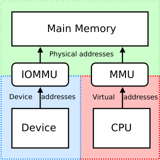
In computing, an input–output memory management unit (IOMMU) is a memory management unit (MMU) connecting a direct-memory-access–capable (DMA-capable) I/O bus to the main memory. Like a traditional MMU, which translates CPU-visible virtual addresses to physical addresses, the IOMMU maps device-visible virtual addresses to physical addresses. Some units also provide memory protection from faulty or malicious devices.

Tolapai is the code name of Intel's embedded system on a chip (SoC) which combines a Pentium M (Dothan) processor core, DDR2 memory controllers and input/output (I/O) controllers, and a QuickAssist integrated accelerator unit for security functions.

<span class="mw-page-title-main">Intel 8237</span> Direct memory access controller

Intel 8237 is a direct memory access (DMA) controller, a part of the MCS 85 microprocessor family. It enables data transfer between memory and the I/O with reduced load on the system's main processor by providing the memory with control signals and memory address information during the DMA transfer.

The NEC μCOM series is a series of microprocessors and microcontrollers manufactured by NEC in the 1970s and 1980s. The initial entries in the series were custom-designed 4 and 16-bit designs, but later models in the series were mostly based on the Intel 8080 and Zilog Z80 8-bit designs, and later, the Intel 8086 16-bit design. Most of the line was replaced in 1984 by the NEC V20, an Intel 8088 clone.

References

  1. https://images.slideplayer.com/26/8671671/slides/slide_5.jpg [ bare URL image file ]
  2. 1 2 Johannes Winter (2011). "A Hijacker's Guide to the LPC bus". tugraz.at. Retrieved 2013-12-19.
  3. Installable LPC Debug Module Design Guide (PDF) (Specification). Revision 1.0. Intel. 2000. p. 15. Archived from the original (PDF) on 2017-06-04.
  4. "BIOS POST Code Reader with the Raspberry Pi Pico" . Retrieved 2024-09-11.
  5. "Industrial motherboard peripherals: EXT-RS232". DFI . Retrieved 2024-09-11.
  6. 1 2 Serialized IRQ Support For PCI Systems (Revision 6.0; September 1, 1995)
  7. 1 2 3 4 5 6 7 "Intel Chipsets Low Pin Count Interface Specification". www.intel.com. Intel. Archived from the original on 2017-02-14.
  8. Dagan, Sharon (2002-05-03). "Flash Storage Alternatives for the Low-Pin-Count (LPC) Bus". EE Times.
  9. "LPC Bus Controller. Reference Design RD1049". www.latticesemi.com. Lattice Semiconductor. Archived from the original (PDF) on 2013-08-07.
  10. Huang, Andrew (2003). Hacking the Xbox: An Introduction to Reverse Engineering. No Starch Press. pp. 48, 151. ISBN   1-59327-029-1.
  11. O. Theis. "Modding the XBox". section "Details of the LPC".
  12. 1 2 Intel Corp. (2003-04-25), "Chapter 12: ISA Bus" (PDF), PC Architecture for Technicians: Level 1, retrieved 2015-01-27
  13. 1 2 3 "TCG PC Client Platform TPM Profile (PTP) Specification" (PDF). Trusted Computing Group. January 26, 2015. pp. 29, 123–124. Retrieved October 5, 2016..