Related Research Articles

An integrated circuit (IC), also known as a microchip, computer chip, or simply chip, is a small electronic device made up of multiple interconnected electronic components such as transistors, resistors, and capacitors. These components are etched onto a small piece of semiconductor material, usually silicon. Integrated circuits are used in a wide range of electronic devices, including computers, smartphones, and televisions, to perform various functions such as processing and storing information. They have greatly impacted the field of electronics by enabling device miniaturization and enhanced functionality.
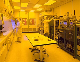
Semiconductor device fabrication is the process used to manufacture semiconductor devices, typically integrated circuits (ICs) such as computer processors, microcontrollers, and memory chips. It is a multiple-step photolithographic and physico-chemical process during which electronic circuits are gradually created on a wafer, typically made of pure single-crystal semiconducting material. Silicon is almost always used, but various compound semiconductors are used for specialized applications.

Moore's law is the observation that the number of transistors in an integrated circuit (IC) doubles about every two years. Moore's law is an observation and projection of a historical trend. Rather than a law of physics, it is an empirical relationship. It is an experience-curve law, a type of law quantifying efficiency gains from experience in production.

Complementary metal–oxide–semiconductor is a type of metal–oxide–semiconductor field-effect transistor (MOSFET) fabrication process that uses complementary and symmetrical pairs of p-type and n-type MOSFETs for logic functions. CMOS technology is used for constructing integrated circuit (IC) chips, including microprocessors, microcontrollers, memory chips, and other digital logic circuits. CMOS technology is also used for analog circuits such as image sensors, data converters, RF circuits, and highly integrated transceivers for many types of communication.
The 90 nm process refers to the technology used in semiconductor manufacturing to create integrated circuits with a minimum feature size of 90 nanometers. It was an advancement over the previous 130 nm process. Eventually, it was succeeded by smaller process nodes, such as the 65 nm, 45 nm, and 32 nm processes.
Semiconductor memory is a digital electronic semiconductor device used for digital data storage, such as computer memory. It typically refers to devices in which data is stored within metal–oxide–semiconductor (MOS) memory cells on a silicon integrated circuit memory chip. There are numerous different types using different semiconductor technologies. The two main types of random-access memory (RAM) are static RAM (SRAM), which uses several transistors per memory cell, and dynamic RAM (DRAM), which uses a transistor and a MOS capacitor per cell. Non-volatile memory uses floating-gate memory cells, which consist of a single floating-gate transistor per cell.
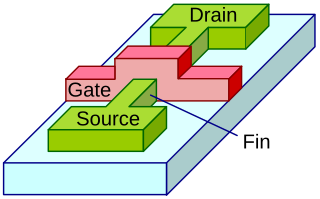
A fin field-effect transistor (FinFET) is a multigate device, a MOSFET built on a substrate where the gate is placed on two, three, or four sides of the channel or wrapped around the channel, forming a double or even multi gate structure. These devices have been given the generic name "FinFETs" because the source/drain region forms fins on the silicon surface. The FinFET devices have significantly faster switching times and higher current density than planar CMOS technology.

An image sensor or imager is a sensor that detects and conveys information used to form an image. It does so by converting the variable attenuation of light waves into signals, small bursts of current that convey the information. The waves can be light or other electromagnetic radiation. Image sensors are used in electronic imaging devices of both analog and digital types, which include digital cameras, camera modules, camera phones, optical mouse devices, medical imaging equipment, night vision equipment such as thermal imaging devices, radar, sonar, and others. As technology changes, electronic and digital imaging tends to replace chemical and analog imaging.
SONOS, short for "silicon–oxide–nitride–oxide–silicon", more precisely, "polycrystalline silicon"—"silicon dioxide"—"silicon nitride"—"silicon dioxide"—"silicon", is a cross sectional structure of MOSFET (metal–oxide–semiconductor field-effect transistor), realized by P.C.Y. Chen of Fairchild Camera and Instrument in 1977. This structure is often used for non-volatile memories, such as EEPROM and flash memories. It is sometimes used for TFT LCD displays. It is one of CTF (charge trap flash) variants. It is distinguished from traditional non-volatile memory structures by the use of silicon nitride (Si3N4 or Si9N10) instead of "polysilicon-based FG (floating-gate)" for the charge storage material. A further variant is "SHINOS" ("silicon"—"hi-k"—"nitride"—"oxide"—"silicon"), which is substituted top oxide layer with high-κ material. Another advanced variant is "MONOS" ("metal–oxide–nitride–oxide–silicon"). Companies offering SONOS-based products include Cypress Semiconductor, Macronix, Toshiba, United Microelectronics Corporation and FloadiaArchived 2022-11-01 at the Wayback Machine.
The "14 nanometer process" refers to a marketing term for the MOSFET technology node that is the successor to the "22 nm" node. The "14 nm" was so named by the International Technology Roadmap for Semiconductors (ITRS). Until about 2011, the node following "22 nm" was expected to be "16 nm". All "14 nm" nodes use FinFET technology, a type of multi-gate MOSFET technology that is a non-planar evolution of planar silicon CMOS technology.

A multigate device, multi-gate MOSFET or multi-gate field-effect transistor (MuGFET) refers to a metal–oxide–semiconductor field-effect transistor (MOSFET) that has more than one gate on a single transistor. The multiple gates may be controlled by a single gate electrode, wherein the multiple gate surfaces act electrically as a single gate, or by independent gate electrodes. A multigate device employing independent gate electrodes is sometimes called a multiple-independent-gate field-effect transistor (MIGFET). The most widely used multi-gate devices are the FinFET and the GAAFET, which are non-planar transistors, or 3D transistors.
Nanocircuits are electrical circuits operating on the nanometer scale where quantum mechanical effects become important. One nanometer is equal to 10−9 meters or a row of 10 hydrogen atoms. With such progressively smaller circuits, more can be fitted on a computer chip. This allows faster and more complex functions using less power. Nanocircuits are composed of three different fundamental components. These are transistors, interconnections, and architecture, all fabricated on the nanometer scale.
A three-dimensional integrated circuit is a MOS integrated circuit (IC) manufactured by stacking as many as 16 or more ICs and interconnecting them vertically using, for instance, through-silicon vias (TSVs) or Cu-Cu connections, so that they behave as a single device to achieve performance improvements at reduced power and smaller footprint than conventional two dimensional processes. The 3D IC is one of several 3D integration schemes that exploit the z-direction to achieve electrical performance benefits in microelectronics and nanoelectronics.

Fujio Masuoka is a Japanese engineer, who has worked for Toshiba and Tohoku University, and is currently chief technical officer (CTO) of Unisantis Electronics. He is best known as the inventor of flash memory, including the development of both the NOR flash and NAND flash types in the 1980s. He also invented the first gate-all-around (GAA) MOSFET (GAAFET) transistor, an early non-planar 3D transistor, in 1988.
Random-access memory is a form of electronic computer memory that can be read and changed in any order, typically used to store working data and machine code. A random-access memory device allows data items to be read or written in almost the same amount of time irrespective of the physical location of data inside the memory, in contrast with other direct-access data storage media, where the time required to read and write data items varies significantly depending on their physical locations on the recording medium, due to mechanical limitations such as media rotation speeds and arm movement.
In semiconductor manufacturing, the International Roadmap for Devices and Systems defines the "5 nm" process as the MOSFET technology node following the "7 nm" node. In 2020, Samsung and TSMC entered volume production of "5 nm" chips, manufactured for companies including Apple, Huawei, Mediatek, Qualcomm and Marvell.
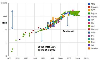
Beyond CMOS refers to the possible future digital logic technologies beyond the scaling limits of CMOS technology. which limits device density and speeds due to heating effects.

Dr. Gary Patton is an American technologist and business executive. He is currently the Corporate Vice President and General Manager of Design Enablement and Components Research in the Technology Development Group at Intel. He has spent most of his career in IBM, starting in IBM's Research Division and holding management and executive positions in IBM's Microelectronics Division in Technology Development, Design Enablement, Manufacturing, and Business Line Management.

Tsu-Jae King Liu is an American academic and engineer who serves as the Dean and the Roy W. Carlson Professor of Engineering at the UC Berkeley College of Engineering.
References
- ↑ "Conference Reflections". Nature Electronics. 2019-12-16.
- ↑ Teschler, Lee (2019-12-10). "Researchers find ways to integrate GaN power circuits onto ICs". EE World.
- ↑ "1965: "Moore's Law" Predicts the Future of Integrated Circuits | The Silicon Engine | Computer History Museum". Computerhistory.org. Retrieved 2017-03-11.
- ↑ "The economics of chip manufacture on advanced technologies". Newelectronics.co.uk. 2011-07-26. Retrieved 2017-03-11.
- ↑ McEwan, A.W. (April 1956). "A production model K-band backward wave oscillator". IRE Transactions on Electron Devices. 3 (2): 108. Bibcode:1956ITED....3..108M. doi:10.1109/T-ED.1956.14115.
- ↑ Paul McLellan (2015-12-11). "IEDM: the International Electron Devices Meeting - Breakfast Bytes - Cadence Blogs - Cadence Community". Community.cadence.com. Retrieved 2017-03-11.
- ↑ sdavis (2015-12-02). "A Look Ahead at IEDM 2015 | Siliconica". Electroiq.com. Retrieved 2017-03-11.
- ↑ Stevenson, Richard (2016-01-26). "Nanowire Transistors Could Let You Talk, Text, and Tweet Longer - IEEE Spectrum". IEEE . Retrieved 2017-03-11.
- ↑ Tetsuo Nozawa (2015-12-24). "Samsung: DRAM Can Be Scaled Down to 10nm - Nikkei Technology Online". Techon.nikkeibp.co.jp. Retrieved 2017-03-11.
- ↑ "IEDM Blogs – Part 3 – Global Foundries 22FDX Briefing". SemiWiki.com. Retrieved 2017-03-11.
- ↑ Ashok Bindra. "IEDM Divulges Advances in Wide Bandgap Devices | Electronics360". Electronics360.globalspec.com. Retrieved 2017-03-11.
- ↑ Turley, Jim (2016-02-01). "How It's Built: Micron/Intel 3D NAND". Eejournal.com. Retrieved 2017-03-11.
- ↑ "Germanium-tin laser for silicon photonics is CMOS compatible". laserfocusworld.com. 17 November 2015. Retrieved 11 March 2017.
- ↑ "2015 IEDM Slide 11: RF CMOS Circuits on Flexible, Application-Specific Substrates | Chip Design". Eecatalog.com. 2016-02-09. Retrieved 2017-03-11.
- ↑ "IEDM 2015 NV Memory and Brain Functions". EE Times. Retrieved 2017-03-11.
- ↑ "5 Takeaways From IEDM" (December 15, 2016), Mark Lapedus, Semiconductor Engineering
- ↑ "IEDM 2016 - 7nm Shootout" (January 17, 2016), Scotten Jones, SemiWiki.com
- ↑ "How It’s Built: Micron/Intel 3D NAND" (February 1, 2016), Bryon Moyer, EE Journal
- ↑ "RRAM/PCM-Based Brain-Gates Emerge as New Components" (February 28, 2017), Ron Neale, EE Times
- ↑ "Graphene Temporary Tattoo Tracks Vital Signs" (January 11, 2017) by Katherine Bourzac, IEEE Spectrum
- ↑ "System-Level Impact of WBG Power Devices at 2016 IEDM" (October 26, 2016), PowerPulse.net
- ↑ "Copper Interconnects" IBM 100 Icons of Progress
- ↑ "IEDM 2019 Keynotes and Memory Technology". The Media News. 2019-12-18.
- ↑ McLellan, Paul (2019-12-19). "IEDM 2019: An Overview...Plus the Future of EUV". Breakfast Bytes.
- ↑ Stelzer, Gerhard (2020-02-13). "The Future of Non-Volatile Memory". Elektronik.
- ↑ Draper, Don. "TSMC Unveils Details of 5nm CMOS Production Technology Platform Featuring EUV and High Mobility Channel FinFETs at IEDM 2019". SemiWiki.com.
- ↑ Moore, Samuel (2020-01-29). "New Nonvolatile Memories Shrink Circuits That Search Fast". IEEE Spectrum.
- ↑ McLellan, Paul (12 January 2021). "IEDM Opening Keynote". Breakfast Bytes. Cadence Corp. Retrieved 18 January 2021.
- ↑ Moyer, Bryon (14 January 2021). "More Data, More Memory-Scaling Problems". Semiconductor Engineering. Sperling Media Group LLC.
- ↑ Moore, Samuel (29 December 2020). "Intel's Stacked Nanosheet Transistors Could Be the Next Step in Moore's Law". IEEE Spectrum.
- ↑ Dillinger, Tom (16 December 2020). "Advanced Process Development is Much More than just Litho". SemiWiki.com.
- ↑ "Highlights from the 2022 IEEE International Electron Devices Meeting". Nature Electronics. Nature. 2 December 2022. Retrieved 22 September 2023.
- ↑ "Podcast EP196: A Look at the Upcoming IEDM Conference with the Publicity Chair and Vice Chair".