US9196201B2 - Method for controlling electro-optic device, device for controlling electro-optic device, electro-optic device, and electronic apparatus - Google Patents
Method for controlling electro-optic device, device for controlling electro-optic device, electro-optic device, and electronic apparatus Download PDFInfo
- Publication number
- US9196201B2 US9196201B2 US13/830,546 US201313830546A US9196201B2 US 9196201 B2 US9196201 B2 US 9196201B2 US 201313830546 A US201313830546 A US 201313830546A US 9196201 B2 US9196201 B2 US 9196201B2
- Authority
- US
- United States
- Prior art keywords
- optical state
- control step
- pixel
- voltage pulse
- voltage
- Prior art date
- Legal status (The legal status is an assumption and is not a legal conclusion. Google has not performed a legal analysis and makes no representation as to the accuracy of the status listed.)
- Expired - Fee Related, expires
Links
- 238000000034 method Methods 0.000 title claims abstract description 60
- 230000003287 optical effect Effects 0.000 claims abstract description 259
- 229910052721 tungsten Inorganic materials 0.000 claims abstract description 6
- 230000008569 process Effects 0.000 claims description 8
- 230000007423 decrease Effects 0.000 claims description 6
- 239000000382 optic material Substances 0.000 claims description 6
- 239000002245 particle Substances 0.000 description 55
- 230000008859 change Effects 0.000 description 20
- 239000003094 microcapsule Substances 0.000 description 15
- 239000000758 substrate Substances 0.000 description 13
- 238000013459 approach Methods 0.000 description 6
- 238000010586 diagram Methods 0.000 description 6
- 230000014759 maintenance of location Effects 0.000 description 6
- 239000002612 dispersion medium Substances 0.000 description 5
- -1 ethyl acetate Chemical class 0.000 description 5
- 239000011159 matrix material Substances 0.000 description 5
- RRLHMJHRFMHVNM-BQVXCWBNSA-N [(2s,3r,6r)-6-[5-[5-hydroxy-3-(4-hydroxyphenyl)-4-oxochromen-7-yl]oxypentoxy]-2-methyl-3,6-dihydro-2h-pyran-3-yl] acetate Chemical compound C1=C[C@@H](OC(C)=O)[C@H](C)O[C@H]1OCCCCCOC1=CC(O)=C2C(=O)C(C=3C=CC(O)=CC=3)=COC2=C1 RRLHMJHRFMHVNM-BQVXCWBNSA-N 0.000 description 4
- 230000006866 deterioration Effects 0.000 description 4
- 239000000049 pigment Substances 0.000 description 4
- 238000011160 research Methods 0.000 description 4
- ZWEHNKRNPOVVGH-UHFFFAOYSA-N 2-Butanone Chemical compound CCC(C)=O ZWEHNKRNPOVVGH-UHFFFAOYSA-N 0.000 description 3
- CSCPPACGZOOCGX-UHFFFAOYSA-N Acetone Chemical compound CC(C)=O CSCPPACGZOOCGX-UHFFFAOYSA-N 0.000 description 3
- UHOVQNZJYSORNB-UHFFFAOYSA-N Benzene Chemical compound C1=CC=CC=C1 UHOVQNZJYSORNB-UHFFFAOYSA-N 0.000 description 3
- YMWUJEATGCHHMB-UHFFFAOYSA-N Dichloromethane Chemical compound ClCCl YMWUJEATGCHHMB-UHFFFAOYSA-N 0.000 description 3
- LFQSCWFLJHTTHZ-UHFFFAOYSA-N Ethanol Chemical compound CCO LFQSCWFLJHTTHZ-UHFFFAOYSA-N 0.000 description 3
- XEKOWRVHYACXOJ-UHFFFAOYSA-N Ethyl acetate Chemical compound CCOC(C)=O XEKOWRVHYACXOJ-UHFFFAOYSA-N 0.000 description 3
- OKKJLVBELUTLKV-UHFFFAOYSA-N Methanol Chemical compound OC OKKJLVBELUTLKV-UHFFFAOYSA-N 0.000 description 3
- YXFVVABEGXRONW-UHFFFAOYSA-N Toluene Chemical compound CC1=CC=CC=C1 YXFVVABEGXRONW-UHFFFAOYSA-N 0.000 description 3
- XLOMVQKBTHCTTD-UHFFFAOYSA-N Zinc monoxide Chemical compound [Zn]=O XLOMVQKBTHCTTD-UHFFFAOYSA-N 0.000 description 3
- 239000012528 membrane Substances 0.000 description 3
- VLKZOEOYAKHREP-UHFFFAOYSA-N n-Hexane Chemical compound CCCCCC VLKZOEOYAKHREP-UHFFFAOYSA-N 0.000 description 3
- 239000011347 resin Substances 0.000 description 3
- 229920005989 resin Polymers 0.000 description 3
- KBPLFHHGFOOTCA-UHFFFAOYSA-N 1-Octanol Chemical compound CCCCCCCCO KBPLFHHGFOOTCA-UHFFFAOYSA-N 0.000 description 2
- HEDRZPFGACZZDS-UHFFFAOYSA-N Chloroform Chemical compound ClC(Cl)Cl HEDRZPFGACZZDS-UHFFFAOYSA-N 0.000 description 2
- LTEQMZWBSYACLV-UHFFFAOYSA-N Hexylbenzene Chemical compound CCCCCCC1=CC=CC=C1 LTEQMZWBSYACLV-UHFFFAOYSA-N 0.000 description 2
- KFZMGEQAYNKOFK-UHFFFAOYSA-N Isopropanol Chemical compound CC(C)O KFZMGEQAYNKOFK-UHFFFAOYSA-N 0.000 description 2
- LRHPLDYGYMQRHN-UHFFFAOYSA-N N-Butanol Chemical compound CCCCO LRHPLDYGYMQRHN-UHFFFAOYSA-N 0.000 description 2
- OFBQJSOFQDEBGM-UHFFFAOYSA-N Pentane Chemical compound CCCCC OFBQJSOFQDEBGM-UHFFFAOYSA-N 0.000 description 2
- GWEVSGVZZGPLCZ-UHFFFAOYSA-N Titan oxide Chemical compound O=[Ti]=O GWEVSGVZZGPLCZ-UHFFFAOYSA-N 0.000 description 2
- 239000012790 adhesive layer Substances 0.000 description 2
- 239000011230 binding agent Substances 0.000 description 2
- OCKPCBLVNKHBMX-UHFFFAOYSA-N butylbenzene Chemical compound CCCCC1=CC=CC=C1 OCKPCBLVNKHBMX-UHFFFAOYSA-N 0.000 description 2
- 230000001413 cellular effect Effects 0.000 description 2
- 239000000084 colloidal system Substances 0.000 description 2
- 239000007822 coupling agent Substances 0.000 description 2
- UZILCZKGXMQEQR-UHFFFAOYSA-N decyl-Benzene Chemical compound CCCCCCCCCCC1=CC=CC=C1 UZILCZKGXMQEQR-UHFFFAOYSA-N 0.000 description 2
- 230000000694 effects Effects 0.000 description 2
- 230000006870 function Effects 0.000 description 2
- 239000011521 glass Substances 0.000 description 2
- 239000000463 material Substances 0.000 description 2
- UAEPNZWRGJTJPN-UHFFFAOYSA-N methylcyclohexane Chemical compound CC1CCCCC1 UAEPNZWRGJTJPN-UHFFFAOYSA-N 0.000 description 2
- 238000012986 modification Methods 0.000 description 2
- 230000004048 modification Effects 0.000 description 2
- 239000003921 oil Substances 0.000 description 2
- 239000004033 plastic Substances 0.000 description 2
- 229920003023 plastic Polymers 0.000 description 2
- 229920000642 polymer Polymers 0.000 description 2
- 239000004094 surface-active agent Substances 0.000 description 2
- VZGDMQKNWNREIO-UHFFFAOYSA-N tetrachloromethane Chemical compound ClC(Cl)(Cl)Cl VZGDMQKNWNREIO-UHFFFAOYSA-N 0.000 description 2
- MCVUKOYZUCWLQQ-UHFFFAOYSA-N tridecylbenzene Chemical compound CCCCCCCCCCCCCC1=CC=CC=C1 MCVUKOYZUCWLQQ-UHFFFAOYSA-N 0.000 description 2
- 235000014692 zinc oxide Nutrition 0.000 description 2
- 239000011787 zinc oxide Substances 0.000 description 2
- WSLDOOZREJYCGB-UHFFFAOYSA-N 1,2-Dichloroethane Chemical compound ClCCCl WSLDOOZREJYCGB-UHFFFAOYSA-N 0.000 description 1
- XNWFRZJHXBZDAG-UHFFFAOYSA-N 2-METHOXYETHANOL Chemical compound COCCO XNWFRZJHXBZDAG-UHFFFAOYSA-N 0.000 description 1
- FWLHAQYOFMQTHQ-UHFFFAOYSA-N 2-N-[8-[[8-(4-aminoanilino)-10-phenylphenazin-10-ium-2-yl]amino]-10-phenylphenazin-10-ium-2-yl]-8-N,10-diphenylphenazin-10-ium-2,8-diamine hydroxy-oxido-dioxochromium Chemical compound O[Cr]([O-])(=O)=O.O[Cr]([O-])(=O)=O.O[Cr]([O-])(=O)=O.Nc1ccc(Nc2ccc3nc4ccc(Nc5ccc6nc7ccc(Nc8ccc9nc%10ccc(Nc%11ccccc%11)cc%10[n+](-c%10ccccc%10)c9c8)cc7[n+](-c7ccccc7)c6c5)cc4[n+](-c4ccccc4)c3c2)cc1 FWLHAQYOFMQTHQ-UHFFFAOYSA-N 0.000 description 1
- 239000004925 Acrylic resin Substances 0.000 description 1
- 229920000178 Acrylic resin Polymers 0.000 description 1
- DKPFZGUDAPQIHT-UHFFFAOYSA-N Butyl acetate Natural products CCCCOC(C)=O DKPFZGUDAPQIHT-UHFFFAOYSA-N 0.000 description 1
- XDTMQSROBMDMFD-UHFFFAOYSA-N Cyclohexane Chemical compound C1CCCCC1 XDTMQSROBMDMFD-UHFFFAOYSA-N 0.000 description 1
- 108010010803 Gelatin Proteins 0.000 description 1
- 229920000084 Gum arabic Polymers 0.000 description 1
- NTIZESTWPVYFNL-UHFFFAOYSA-N Methyl isobutyl ketone Chemical compound CC(C)CC(C)=O NTIZESTWPVYFNL-UHFFFAOYSA-N 0.000 description 1
- UIHCLUNTQKBZGK-UHFFFAOYSA-N Methyl isobutyl ketone Natural products CCC(C)C(C)=O UIHCLUNTQKBZGK-UHFFFAOYSA-N 0.000 description 1
- CTQNGGLPUBDAKN-UHFFFAOYSA-N O-Xylene Chemical compound CC1=CC=CC=C1C CTQNGGLPUBDAKN-UHFFFAOYSA-N 0.000 description 1
- 229920006662 PF-NF Polymers 0.000 description 1
- 241000978776 Senegalia senegal Species 0.000 description 1
- 239000006087 Silane Coupling Agent Substances 0.000 description 1
- RTAQQCXQSZGOHL-UHFFFAOYSA-N Titanium Chemical compound [Ti] RTAQQCXQSZGOHL-UHFFFAOYSA-N 0.000 description 1
- 229920001807 Urea-formaldehyde Polymers 0.000 description 1
- 235000010489 acacia gum Nutrition 0.000 description 1
- 239000000205 acacia gum Substances 0.000 description 1
- 239000000853 adhesive Substances 0.000 description 1
- 230000001070 adhesive effect Effects 0.000 description 1
- 239000005456 alcohol based solvent Substances 0.000 description 1
- 150000001338 aliphatic hydrocarbons Chemical class 0.000 description 1
- 125000000217 alkyl group Chemical group 0.000 description 1
- 229910052782 aluminium Inorganic materials 0.000 description 1
- XAGFODPZIPBFFR-UHFFFAOYSA-N aluminium Chemical compound [Al] XAGFODPZIPBFFR-UHFFFAOYSA-N 0.000 description 1
- 229910000410 antimony oxide Inorganic materials 0.000 description 1
- 150000004945 aromatic hydrocarbons Chemical class 0.000 description 1
- 150000001555 benzenes Chemical class 0.000 description 1
- 239000003990 capacitor Substances 0.000 description 1
- 239000006229 carbon black Substances 0.000 description 1
- 150000007942 carboxylates Chemical class 0.000 description 1
- 239000003795 chemical substances by application Substances 0.000 description 1
- 239000003086 colorant Substances 0.000 description 1
- 150000001875 compounds Chemical class 0.000 description 1
- 239000004020 conductor Substances 0.000 description 1
- 239000002270 dispersing agent Substances 0.000 description 1
- KWKXNDCHNDYVRT-UHFFFAOYSA-N dodecylbenzene Chemical compound CCCCCCCCCCCCC1=CC=CC=C1 KWKXNDCHNDYVRT-UHFFFAOYSA-N 0.000 description 1
- 230000005684 electric field Effects 0.000 description 1
- 239000003792 electrolyte Substances 0.000 description 1
- 150000002148 esters Chemical class 0.000 description 1
- 239000008273 gelatin Substances 0.000 description 1
- 229920000159 gelatin Polymers 0.000 description 1
- 235000019322 gelatine Nutrition 0.000 description 1
- 235000011852 gelatine desserts Nutrition 0.000 description 1
- 150000008282 halocarbons Chemical class 0.000 description 1
- FUZZWVXGSFPDMH-UHFFFAOYSA-N hexanoic acid Chemical compound CCCCCC(O)=O FUZZWVXGSFPDMH-UHFFFAOYSA-N 0.000 description 1
- 229930195733 hydrocarbon Natural products 0.000 description 1
- AMGQUBHHOARCQH-UHFFFAOYSA-N indium;oxotin Chemical compound [In].[Sn]=O AMGQUBHHOARCQH-UHFFFAOYSA-N 0.000 description 1
- 150000002576 ketones Chemical class 0.000 description 1
- 239000010410 layer Substances 0.000 description 1
- 239000000314 lubricant Substances 0.000 description 1
- SJCKRGFTWFGHGZ-UHFFFAOYSA-N magnesium silver Chemical compound [Mg].[Ag] SJCKRGFTWFGHGZ-UHFFFAOYSA-N 0.000 description 1
- 238000004519 manufacturing process Methods 0.000 description 1
- 229910052751 metal Inorganic materials 0.000 description 1
- 239000002184 metal Substances 0.000 description 1
- GYNNXHKOJHMOHS-UHFFFAOYSA-N methyl-cycloheptane Natural products CC1CCCCCC1 GYNNXHKOJHMOHS-UHFFFAOYSA-N 0.000 description 1
- LIXVMPBOGDCSRM-UHFFFAOYSA-N nonylbenzene Chemical compound CCCCCCCCCC1=CC=CC=C1 LIXVMPBOGDCSRM-UHFFFAOYSA-N 0.000 description 1
- TVMXDCGIABBOFY-UHFFFAOYSA-N octane Chemical compound CCCCCCCC TVMXDCGIABBOFY-UHFFFAOYSA-N 0.000 description 1
- VXNSQGRKHCZUSU-UHFFFAOYSA-N octylbenzene Chemical compound [CH2]CCCCCCCC1=CC=CC=C1 VXNSQGRKHCZUSU-UHFFFAOYSA-N 0.000 description 1
- VTRUBDSFZJNXHI-UHFFFAOYSA-N oxoantimony Chemical compound [Sb]=O VTRUBDSFZJNXHI-UHFFFAOYSA-N 0.000 description 1
- 230000003071 parasitic effect Effects 0.000 description 1
- 238000005192 partition Methods 0.000 description 1
- 229920001483 poly(ethyl methacrylate) polymer Polymers 0.000 description 1
- 229920003229 poly(methyl methacrylate) Polymers 0.000 description 1
- 229920000767 polyaniline Polymers 0.000 description 1
- 239000002952 polymeric resin Substances 0.000 description 1
- 239000004926 polymethyl methacrylate Substances 0.000 description 1
- 239000000843 powder Substances 0.000 description 1
- 238000012545 processing Methods 0.000 description 1
- 238000002310 reflectometry Methods 0.000 description 1
- 230000000717 retained effect Effects 0.000 description 1
- 239000005060 rubber Substances 0.000 description 1
- 239000000344 soap Substances 0.000 description 1
- 239000002904 solvent Substances 0.000 description 1
- 239000003381 stabilizer Substances 0.000 description 1
- 229920003002 synthetic resin Polymers 0.000 description 1
- JZALLXAUNPOCEU-UHFFFAOYSA-N tetradecylbenzene Chemical compound CCCCCCCCCCCCCCC1=CC=CC=C1 JZALLXAUNPOCEU-UHFFFAOYSA-N 0.000 description 1
- 239000010936 titanium Substances 0.000 description 1
- 229910052719 titanium Inorganic materials 0.000 description 1
- 239000004408 titanium dioxide Substances 0.000 description 1
- XBEADGFTLHRJRB-UHFFFAOYSA-N undecylbenzene Chemical compound CCCCCCCCCCCC1=CC=CC=C1 XBEADGFTLHRJRB-UHFFFAOYSA-N 0.000 description 1
- 239000002966 varnish Substances 0.000 description 1
- XLYOFNOQVPJJNP-UHFFFAOYSA-N water Substances O XLYOFNOQVPJJNP-UHFFFAOYSA-N 0.000 description 1
- 239000012463 white pigment Substances 0.000 description 1
- 210000000707 wrist Anatomy 0.000 description 1
- 239000008096 xylene Substances 0.000 description 1
- YVTHLONGBIQYBO-UHFFFAOYSA-N zinc indium(3+) oxygen(2-) Chemical compound [O--].[Zn++].[In+3] YVTHLONGBIQYBO-UHFFFAOYSA-N 0.000 description 1
Images


Classifications
-
- G—PHYSICS
- G09—EDUCATION; CRYPTOGRAPHY; DISPLAY; ADVERTISING; SEALS
- G09G—ARRANGEMENTS OR CIRCUITS FOR CONTROL OF INDICATING DEVICES USING STATIC MEANS TO PRESENT VARIABLE INFORMATION
- G09G3/00—Control arrangements or circuits, of interest only in connection with visual indicators other than cathode-ray tubes
- G09G3/20—Control arrangements or circuits, of interest only in connection with visual indicators other than cathode-ray tubes for presentation of an assembly of a number of characters, e.g. a page, by composing the assembly by combination of individual elements arranged in a matrix no fixed position being assigned to or needed to be assigned to the individual characters or partial characters
- G09G3/34—Control arrangements or circuits, of interest only in connection with visual indicators other than cathode-ray tubes for presentation of an assembly of a number of characters, e.g. a page, by composing the assembly by combination of individual elements arranged in a matrix no fixed position being assigned to or needed to be assigned to the individual characters or partial characters by control of light from an independent source
- G09G3/3433—Control arrangements or circuits, of interest only in connection with visual indicators other than cathode-ray tubes for presentation of an assembly of a number of characters, e.g. a page, by composing the assembly by combination of individual elements arranged in a matrix no fixed position being assigned to or needed to be assigned to the individual characters or partial characters by control of light from an independent source using light modulating elements actuated by an electric field and being other than liquid crystal devices and electrochromic devices
- G09G3/344—Control arrangements or circuits, of interest only in connection with visual indicators other than cathode-ray tubes for presentation of an assembly of a number of characters, e.g. a page, by composing the assembly by combination of individual elements arranged in a matrix no fixed position being assigned to or needed to be assigned to the individual characters or partial characters by control of light from an independent source using light modulating elements actuated by an electric field and being other than liquid crystal devices and electrochromic devices based on particles moving in a fluid or in a gas, e.g. electrophoretic devices
-
- G—PHYSICS
- G09—EDUCATION; CRYPTOGRAPHY; DISPLAY; ADVERTISING; SEALS
- G09G—ARRANGEMENTS OR CIRCUITS FOR CONTROL OF INDICATING DEVICES USING STATIC MEANS TO PRESENT VARIABLE INFORMATION
- G09G2300/00—Aspects of the constitution of display devices
- G09G2300/08—Active matrix structure, i.e. with use of active elements, inclusive of non-linear two terminal elements, in the pixels together with light emitting or modulating elements
- G09G2300/0809—Several active elements per pixel in active matrix panels
- G09G2300/0842—Several active elements per pixel in active matrix panels forming a memory circuit, e.g. a dynamic memory with one capacitor
-
- G—PHYSICS
- G09—EDUCATION; CRYPTOGRAPHY; DISPLAY; ADVERTISING; SEALS
- G09G—ARRANGEMENTS OR CIRCUITS FOR CONTROL OF INDICATING DEVICES USING STATIC MEANS TO PRESENT VARIABLE INFORMATION
- G09G2310/00—Command of the display device
- G09G2310/06—Details of flat display driving waveforms
-
- G—PHYSICS
- G09—EDUCATION; CRYPTOGRAPHY; DISPLAY; ADVERTISING; SEALS
- G09G—ARRANGEMENTS OR CIRCUITS FOR CONTROL OF INDICATING DEVICES USING STATIC MEANS TO PRESENT VARIABLE INFORMATION
- G09G3/00—Control arrangements or circuits, of interest only in connection with visual indicators other than cathode-ray tubes
- G09G3/20—Control arrangements or circuits, of interest only in connection with visual indicators other than cathode-ray tubes for presentation of an assembly of a number of characters, e.g. a page, by composing the assembly by combination of individual elements arranged in a matrix no fixed position being assigned to or needed to be assigned to the individual characters or partial characters
- G09G3/2007—Display of intermediate tones
Definitions
- the present invention relates to methods for controlling an electro-optic device, devices for controlling an electro-optic device, electro-optic devices, and electronic apparatuses.
- An electrophoretic display device is one example of the electro-optical devices described above.
- the electrophoretic display device displays images at a display section by applying voltages between pixel electrodes and an opposing counter electrode with electrophoretic elements containing electrophoretic particles sandwiched therebetween, thereby migrating electrophoretic particles, such as, black particles and white particles.
- the electrophoretic elements are composed of a plurality of microcapsules each containing a plurality of electrophoretic particles, and affixed between the pixel electrodes and the counter electrode with an adhesive composed of resin or the like.
- the counter electrode may also be called a common electrode.
- white color can be displayed by applying a voltage that moves white particles to the display surface side
- black color can be display by applying voltage that moves black particles to the display surface side.
- an intermediate gray level between white color and black color in other words, gray color
- U.S. Published Patent Application 2005/0001812 Patent Document 1
- U.S. Published Patent Application 2005/0280626 Patent Document 2
- WIPO Published Patent Application WO/2005/101363 Patent Document 3
- each of the particles may only have to be moved to the middle position between white and black displays.
- a control is difficult, and variations might be generated in the gray level to be displayed because, for example, differences occur in the positions of the respective particles.
- the variations described above greatly impact on the display image.
- each particle when the gray level is changed from light gray (that is, gray color close to white) to dark gray (that is, gray color close to black), each particle may be once moved to the position for displaying the white color or the black color from the state where the light gray is displayed, and then moved to the position for displaying the dark gray.
- the positions of the particles for each of the pixels can be made uniform and the intermediate gray level can be suitably displayed.
- bias may be caused in the polarities of the voltages impressed to the pixels through the overall rewriting process. Concretely, a difference may occur between the period in which the voltage with a polarity corresponding to white is impressed and the period in which the voltage with a polarity corresponding to black is impressed.
- a method for controlling an electro-optic device a device for controlling an electro-optic device, an electro-optic device, and an electronic apparatus, which can prevent a bias from being generated in polarities of voltage to be applied to pixels, and therefore can excellently display intermediate gray levels.
- a control process for changing the pixel to a first intermediate optical state among the plurality of intermediate optical states includes a first control step of supplying a first voltage pulse to the pixel electrode until the pixel reaches the first limit optical state, a second control step of supplying a second voltage pulse having an opposite polarity with respect to the first voltage pulse to the pixel electrode after the first control step such that the pixel becomes closer to the first intermediate optical state, a third control step of supplying a third voltage pulse to the pixel electrode before the first control step, and a fourth control step of supplying a fourth voltage pulse having an opposite polarity with respect to the third voltage pulse to the pixel electrode between the third control step and the first control step.
- An electro-optical device that is controlled by the method of controlling an electro-optical device in accordance with an embodiment of the invention is equipped with a display section including a plurality of pixels arrayed in a matrix at places corresponding to intersections between a plurality of scanning lines and a plurality of data lines.
- the display section has electro-optical material between mutually opposing pixel electrode and counter electrode.
- the plurality of pixels may be able to assume a first limit optical state, a second limit optical state, and a plurality of intermediate optical states between the first limit optical state and the second limit optical state.
- the “limit optical state” is an optical state achieved by impressing a predetermined voltage sufficiently to the electro-optic material in the display section.
- the “limit optical state” in the invention not only means a state in which the optical state does not change at all even if the predetermined voltage impressed further from that optical state, but also includes a wider concept including, for example, an optical state in which plural pixels concurrently assume the limit optical state whereby the optical state of each of the pixels is made uniform to the extent that differences in the optical state among the pixels (to be described later) can be reduced.
- an optical state in which white color is displayed by the white particles being drawn sufficiently to the display surface side, or an optical state in which black color is displayed by the black particles being drawn sufficiently to the display surface side corresponds to the “limit optical state” in accordance with the invention.
- the “intermediate optical state” means an optical state in between the first limit optical state and the second limit optical state, and corresponds, for example, to an optical state in which a gray color is displayed, when the optical state of displaying the white color or the black color is assumed to be the limit optical state as described above.
- the “intermediate optical state” may be achieved by, for example, adjusting the period of impressing the voltage for changing the optical state to the first limit optical state, or the voltage for changing the optical state to the second limit optical state. More concretely, for example, by moving the white particles and the black particles contained in the electrophoretic element to an intermediate position between the positions where white color and black colors are displayed, a gray color that defines the intermediate optical state can be displayed.
- each of the pixels can assume a plurality of intermediate optical states, such as, for example, light gray, dark gray, etc.
- Such plural intermediate optical states can be displayed by adjusting the position of each particle between the pixel electrode and the counter electrode. More concretely, light gray can be displayed by placing white particles at an intermediate position relatively near the display surface side (or, black particles are placed at an intermediate position relatively far from the display surface side), and dark gray can be displayed by placing white particles at an intermediate position relatively far from the display surface side (or, black particles are placed at an intermediate position relatively near the display surface side).
- the display section described above is controlled by the drive part in a manner to display an image corresponding to image data. More concretely, when the electro-optic device according to the embodiment is operating, voltage pulses corresponding to the image data are supplied to each of the pixel electrodes of the plural pixels by the drive part. As a result, the voltage corresponding to the image data is impressed to each of the pixels, and the image corresponding to the image data is displayed in the display section.
- the voltage pulses are supplied to each pixel by the drive part over a plurality of frame periods.
- the voltages are impressed to the pixels in the display section multiple times in the unit of a frame period.
- the plural scanning lines are sequentially selected once in a predetermined order in each frame period, and voltage pulses are supplied to the pixel electrodes at the pixels corresponding to the selected scanning line through the plural data lines.
- the “frame period” here is a predetermined period during which the plural scanning lines are selected once in a predetermined order.
- the supply of the voltage pulse to the pixel electrode at each of the plural pixels is controlled once in each of the consecutive plural frame periods, whereby the image corresponding to the image data is displayed in the display section.
- each of the control steps is performed in the order of the third control step, the fourth control step, the first control step, and the second control step.
- Each of the control steps may include a process step other than the first control step, the second control step, the third control step, and fourth control step.
- a step of supplying a voltage pulse to the pixel electrode of a rewriting pixel may exist besides these four control steps.
- the “first intermediate optical state” here is an intermediate optical state aimed at in rewriting the image, and may be set as one optical state among the plural intermediate optical states that can be assumed by the pixels in the display section.
- a voltage for example, ⁇ 15V
- the first limit optical state for example, white
- rewriting pixels assume the first limit optical state.
- the optical state at the plural pixels can be made uniform by changing it to the limit optical state once before the rewriting pixels are changed to assume the first intermediate optical state.
- the positions of the particles contained in the electrophoretic element can be made uniform.
- the first control step may be omitted.
- a voltage for example, +15V
- the second limit optical state for example, black
- a voltage of a reverse-polarity with respect to the first control step is impressed in the second control step.
- a third voltage pulse is supplied to the pixel electrodes of the rewriting pixels.
- a fourth voltage pulse of a reverse-polarity with respect to the third voltage pulse is supplied to the pixel electrodes of the rewriting pixels.
- the fourth voltage pulse having the same polarity of the second voltage pulse to be supplied in the second control step is supplied in the fourth control step.
- the fourth voltage pulse having the same polarity of the first voltage pulse to be supplied in the first control step is supplied in the fourth control step.
- the “drive voltage” here is a voltage to be impressed to the pixel in each of the first control step, the second control step, the third control step and the fourth control step
- the “drive time” means each period in the first control step, the second control step, the third control step, and the fourth control step (in other words, the period when the drive voltage is impressed).
- the integrated value of the drive voltage and the drive time W (2 ⁇ 5) when the optical state is changed from level 2 to level 5 and the integrated value of the drive voltage and drive time W (5 ⁇ 2) when the optical level is changed from level 5 and to level 2 have equal absolute values.
- the integrated value of the drive voltage and the drive time W (6 ⁇ 4) when the optical state is changed from level 6 to level 4 and the integrated value of the drive voltage and drive time W (4 ⁇ 6) when the optical level is changed from level 4 and to level 6 have equal absolute values.
- the term “equal” refers to a wide concept that includes the state in which the absolute values of the integrated values completely correspond to each other and the state in which these values are close to each other to the extent that the effect of the invention to be described later can be demonstrated.
- a desired intermediate optical state can be suitably achieved.
- a high-quality image can be displayed in the electro-optic device, while achieving high reliability.
- the period in each of the third control step and the fourth control step may be set such that the optical state before the beginning of the third control step is the same as the optical state after the end of the fourth control step.
- the optical state of the pixels rewritten does not change before and after these steps. Therefore, the period of the first control step and the second control step can be set without depending on the third control step and the fourth control step. Therefore, the period in each of the control steps can be very easily set.
- the third voltage pulse may have the same polarity as that of the second voltage pulse, and the fourth voltage pulse may have the same polarity as that of the first voltage pulse.
- the third voltage pulse of one polarity is first supplied in the third control step, then the fourth voltage pulse and the first voltage pulse of another polarity are supplied one by one in the following fourth control step and the first control step, and the second voltage pulse of the one polarity is supplied again in the second control step.
- the voltage pulses of the same polarity are continuously supplied in the fourth control step and the first control step.
- the processing can be made simpler to the extent that fewer switching of the polarities takes place.
- the second voltage pulse in the second control step, may be supplied to the pixel electrode until the first intermediate optical state or an intermediate optical state that is close to the second limit optical state more than the first intermediate optical state is reached, and the control step for changing the pixel to the first intermediate optical state may further include a fifth control step of supplying a fifth voltage pulse of the same polarity as that of the first voltage pulse to the pixel electrode until the first intermediate optical state is reached, when, after the second control step, the pixel is in an intermediate optical state that is close to the second limit optical state more than the first intermediate optical state.
- the fifth control step is included in the control process.
- the third control step, the fourth control step, the first control step, the second control step, and the fifth control step are performed in this order.
- the optical state of the rewriting pixel after the second control step is the first intermediate optical state or an optical state close to the second limit optical state more than the first intermediate optical state.
- the optical state of the rewriting pixel after the second control step is not brought to an optical state close to the first limit optical state more than the first intermediate optical state.
- a voltage corresponding to the first limit optical state is impressed again to the rewriting pixel that has assumed an optical state close to the second limit optical state more than the first intermediate optical state.
- the optical state of the rewriting pixel is brought close to the first limit optical state. In other words, it is brought close to the first intermediate optical state further.
- the voltage impressed in the fifth control step may be in the same value as the voltage impressed by the first control step, or may be a different value. In other words, the voltage impressed in the first control step and the voltage impressed in the fifth control step may have mutually different values, as long as they are in the same polarity.
- rewriting after the first control step from the first limit optical state to the first intermediate optical state is performed separately in divided two steps, the second control step and the fifth control step. Therefore, even if the optical state of the rewriting pixel assumes an optical state close to the second limit optical state more than the first intermediate optical state, due to rewriting from the first limit optical state in a direction to the second limit optical state in which the change rate of optical state is relatively high (that is, the second control step), the optical state can be fine-tuned by rewriting in a direction to the first limit optical state in which the change rate of optical state is low (that is, the fifth control step). Therefore, the optical state much closer to the first intermediate optical state can be achieved.
- an absolute value of the integrated value W (A ⁇ B) of drive voltage and drive time when changing the pixel from the optical state A to the optical state B becomes greater, as an absolute value of a difference between the optical state A to the optical state B becomes greater.
- an integrated value of drive voltage and drive time W (A ⁇ C ⁇ B) when changing the pixel from the optical state A to an optical state C and then to the optical state B may become equal to the integrated value of drive voltage and drive time W (A ⁇ B) when changing the pixel from the optical state A to the optical state B.
- the period of the third control step and the fourth control step can be set based on the optical state A before the shift and the optical state B after the shift.
- each of the periods of the third control step and the fourth control step is set by using a weight table decided based on the relation between the optical states and the integrated values of drive voltage and drive time.
- the weight table is decided beforehand based on the relation between the optical states and the integrated values of drive voltage and drive time. For example, integrated values of drive voltage and drive time each corresponding to each of the optical states are set to the weight table.
- the period of each of the control steps is set according to a difference between an integrated value corresponding to the optical state before the rewriting and an integrated value corresponding to the optical state after the rewriting.
- the weight table has one weight value for each reference optical state.
- the weight value of an arbitrary optical state Li is WHT(Li) and the weight value of an optical state Lj is WHT(Lj)
- the weight value may be decided in such a manner that the integrated value of drive voltage and drive time W(Li ⁇ Lj) when shifting the pixel from the optical state Li to the optical state Lj becomes proportional to WHT(Lj) ⁇ WHT(Li).
- reference optical states of eight stages from level 0 to level 7 as described above are set in the weight table.
- Values each corresponding to one weight value (in other words, an integrated value of drive voltage and drive time) is set for each of the reference optical states.
- the weight table is decided in such a manner that the integrated value of drive voltage and drive time W(Li ⁇ Lj) when an arbitrary optical state Li is shifted to an optical state Lj becomes proportional to the difference between the weight values corresponding to the respective optical states (that is, WHT(Lj) ⁇ WHT(Li)).
- WHT(Lj) ⁇ WHT(Li) the weight value corresponding to each of the optical states
- the weight table may have one weight value for each reference optical state, and the weight value may be decided in a manner to increase or decrease monotonously with respect to the optical state.
- the greater the level of the optical state the greater the weight value may become (monotonically increase).
- the weight value corresponding to level 1 is larger than the weight value corresponding to level 0, and the weight value corresponding to level 2 is greater than the weight value corresponding to level 1.
- the greater the level of the optical state the smaller the weight value may become (monotonically decrease).
- the weight value corresponding to level 1 is smaller than the weight value corresponding to level 0, and the weight value corresponding to level 2 is smaller than the weight value corresponding to level 1.
- a control device for controlling an electro-optic device in accordance with an embodiment of the invention includes a display section including a plurality of pixels provided at positions corresponding to intersections between mutually intersecting plural scanning lines and plural data lines, each of the pixels including electro-optic material placed between mutually opposing pixel electrode and counter electrode, and capable of assuming a first limit optical state, a second limit optical state and a plurality of intermediate optical states between the first limit optical state and the second limit optical state, and a drive part that supplies, for displaying an image corresponding to image data at the display section, voltage pulses according to the image data to the pixel electrode of each of the pixels in a plurality of frame periods.
- the control device includes, when changing the pixel to a first intermediate optical state among the plurality of intermediate optical states, a first control device that supplies a first voltage pulse to the pixel electrode until the pixel reaches the first limit optical state, a second control device that supplies a second voltage pulse of an opposite polarity with respect to the first voltage pulse to the pixel electrode after the first voltage pulse is supplied by the first control device such that the pixel becomes closer to the first intermediate optical state, a third control device that supplies a third voltage pulse to the pixel electrode before the first voltage pulse is supplied by the first control device, and a fourth control device that supplies a fourth voltage pulse of an opposite polarity with respect to the third voltage pulse to the pixel electrode after the third voltage pulse is supplied by the third control device and before the first voltage pulse is supplied by the first control device.
- control device for controlling an electro-optic device while keeping the DC balance, a desired intermediate optical state can be suitably achieved, similarly to the method of controlling an electro-optic device described above. As a result, a high-quality image can be displayed in the electro-optic device, while achieving high reliability.
- an electro-optic device has the control device for controlling an electro-optic device in accordance with the invention described above (also, including its various modifications).
- the electro-optic device according to the embodiment of the invention is equipped with the control device for controlling an electro-optic device in accordance with the invention described above, a desired intermediate optical state can be suitably achieved, while keeping the DC balance. As a result, an electro-optic device that can display a high-quality image, while achieving high reliability, can be realized.
- an electronic apparatus is equipped with the electro-optic device according to the invention described above (also including its various embodiments).
- the electronic apparatus in accordance with the invention is equipped with the electro-optic device according to the invention described above, various electronic apparatuses, such as, wristwatches, electronic paper, electronic notepads, cellular phones, portable audio equipment and the like, which are dependable and capable of displaying high-quality images, can be realized.
- FIG. 1 is a block diagram showing an overall configuration of an electrophoretic display device in accordance with an embodiment of the invention.
- FIG. 2 is a block diagram showing a configuration around a display section of the electrophoretic display device in accordance with the embodiment.
- FIG. 3 is an equivalent circuit diagram showing an electrical configuration of pixels in accordance with an embodiment.
- FIG. 4 is a cross-sectional view in part of the display section of the electrophoretic display device in accordance with the embodiment.
- FIG. 5 is a graph showing changes in the gray levels when rewriting white color to black color.
- FIG. 6 is a graph showing changes in the gray levels when rewriting black color to white color.
- FIG. 7 is an illustration showing a concept of a voltage application method when an intermediate gray level 4 is displayed.
- FIG. 8 is an illustration showing a concept of a voltage application method when an intermediate gray level 6 is displayed only with Phase A and Phase B.
- FIG. 9 is an illustration showing a concept of a voltage application method when an intermediate gray level 6 is displayed using Phase C.
- FIG. 10 is an illustration showing a concept of a voltage application method when an intermediate gray level 3 is rewritten to an intermediate gray level 5.
- FIG. 11 is an illustration showing a concept of a voltage application method when an intermediate gray level 5 is rewritten to an intermediate gray level 3.
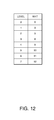
- FIG. 12 is a table figure showing one example of a weight table.
- FIG. 13 is an illustration showing a concept of a voltage application method when a gray level 0 is rewritten to an intermediate gray level 5.
- FIG. 14 is an illustration showing a concept of a voltage application method when an intermediate gray level 1 is rewritten to an intermediate gray level 5.
- FIG. 15 is an illustration showing a concept of a voltage application method when an intermediate gray level 2 is rewritten to an intermediate gray level 5.
- FIG. 16 is an illustration showing a concept of a voltage application method when an intermediate gray level 5 is rewritten to an intermediate gray level 5.
- FIG. 17 is an illustration showing a concept of a voltage application method when a gray level 7 is rewritten to an intermediate gray level 5.
- FIG. 18 is an illustration showing a concept of a voltage application method when an intermediate gray level 5 is rewritten to a gray level 7.
- FIG. 19 is a perspective view showing a configuration of electronic paper that is an example of an electronic apparatus using the electro-optic device.
- FIG. 20 is a perspective view showing a configuration of an electronic notepad that is an example of an electronic apparatus using the electro -optic device.
- FIGS. 1 through 18 An electro-optic device in accordance with the present embodiment will be described with reference to FIGS. 1 through 18 .
- an electrophoretic display device of an active matrix driving type will be enumerated as one example of the electro-optic device in accordance with the invention.
- FIG. 1 is a block diagram showing an overall configuration of the electrophoretic display device in accordance with the present embodiment.
- the electrophoretic display device 1 in accordance with the present embodiment shown in FIG. 1 is equipped with a display section 3 , a ROM 4 , a RAM 5 , a controller 10 , and a CPU 100 .
- the display section 3 is a display device that has a display element having memory property, which maintains a display state even in a state in which writing is not conducted.
- the memory property is a property that, when entering a predetermined display state by application of voltage, would maintain the display state, even when the voltage impression is removed, which is also called bistability. A concrete configuration of the display section 3 will be described in detail later.
- the ROM 4 is a device that stores data to be used when the electrophoretic display device 1 is operated.
- the ROM 4 stores a waveform table of drive voltages to achieve a display state targeted at each of the pixels.
- the waveform table of drive voltages will be described in detail later.
- the ROM 4 can be substituted by a rewritable storage device such as a RAM.
- the RAM 5 is a device that stores data used when the electrophoretic display device 1 is operated, similarly to the ROM 4 described above.
- the RAM 5 stores, for example, data indicative of a display state before a rewriting operation and data indicative of a display state after the rewriting operation, changes.
- the RAM 5 includes a VRAM, etc. that function, for example, as a frame buffer, and stores frame image data based on the control of the CPU 100 .
- the controller 10 controls the display operation of the display section 3 by using the data stored in the ROM 4 and the RAMS described above.
- the controller 10 controls the display section 3 by outputting an image signal indicative of an image to be displayed in the display section 3 and various other signals (for example, a clock signal, etc.)
- the CPU 100 is a processor that controls the operation of the electrophoretic display device 1 , and reads and writes data by executing programs stored in advance.
- the CPU 100 renders the VRAIVI to store image data to be displayed in the display section 3 when the image is rewritten.
- FIG. 2 is a block diagram showing a configuration around the display section of the electrophoretic display device in accordance with the embodiment.
- the electrophoretic display device 1 in accordance with the present embodiment is an electrophoretic display device of an active matrix drive type, and has a display section 3 , a controller 10 , a scanning line drive circuit 60 , a data line drive circuit 70 , and a common potential supply circuit 220 .
- m rows x n columns of pixels 20 are arranged in a matrix (in a two-dimensional plane).
- m scanning lines 40 that is, scanning lines Y 1 , Y 2 , . . . and Ym
- n data lines 50 that is, data lines X 1 , X 2 , . . . and Xn
- the m scanning lines 40 extend in a row direction (i.e., X direction)
- the n data lines 50 extend in a column direction (i.e., Y direction).
- Pixels 20 are disposed at positions corresponding to intersections between the m scanning lines 40 and the n data lines 50 .
- the controller 10 controls the operation of the scanning line drive circuit 60 , the data line drive circuit 70 , and the common potential supply circuit 220 .
- the controller 10 supplies timing signals, such as, for example, a clock signal, a start pulse, etc., to each of the circuits.
- the scanning line drive circuit 60 sequentially supplies a scanning signal in pulses to each of the scanning lines Y 1 , Y 2 , . . . , Ym during a predetermined frame period under the control of the controller 10 .
- the data line drive circuit 70 supplies data potentials to the data lines X 1 , X 2 , . . . , and Xn under the control of the controller 10 .
- the data potential assumes a standard potential GND (for example, 0 volt), a high potential VSH (for example, +15 volt) or a low potential ⁇ VSH (for example, ⁇ 15 volt).
- the common potential supply circuit 220 supplies a common potential Vcom (in the embodiment, the same potential as the reference potential GND) to the common potential line 93 .
- the common potential Vcom may be a potential different from the reference potential GND within the range where a voltage is not substantially generated between the counter electrode 22 to which the common potential Vcom is supplied and the pixel electrode 21 to which the reference potential GND is supplied.
- the common potential Vcom may assume a value different from the reference potential GND supplied to the pixel electrode 21 , in consideration of changes in the potential of the pixel electrode 21 due to feedthrough, and even in this case, the common potential Vcom and the reference potential GND are considered to be the same in the present specification.
- the scanning signal is supplied to the scanning lines 40 , and potentials are supplied to the pixel electrodes 21 through the data lines 50 , and then when the supply of the scanning signal to the scanning lines 40 ends (for example, when the potential on the scanning lines 40 decreases), the potential on the pixel electrodes 21 may fluctuate (for example, decrease with the lowering potential on the scanning lines 40 ) due to the parasitic capacitance between the scanning lines 40 .
- This phenomenon is called feedthrough.
- the common potential Vcom may be set to a value slightly lower than the reference potential GND to be supplied to the pixel electrode 21 . Even in this case, the common potential Vcom and the reference potential GND are considered to be the same potential.
- FIG. 3 is an equivalent circuit diagram of the electrical configuration of pixels in accordance with the present embodiment.
- the pixel 20 is equipped with a pixel switching transistor 24 , a pixel electrode 21 , a counter electrode 22 , an electrophoretic element 23 , and a retention capacitance 27 .
- the pixel switching transistor 24 is formed from, for example, an N type transistor.
- the pixel switching transistor 24 has a gate electrically connected with the scanning line 40 , a source electrically connected with the data line 50 , and a drain electrically connected with the pixel electrode 21 and the retention capacitance 27 .
- the pixel switching transistor 24 outputs data potential supplied from the data line drive circuit 70 (see FIG. 2 ) through the data line 50 to the pixel electrode 21 and the retention capacitor 27 with a timing corresponding to the scanning signal in pulses supplied through the scanning line 40 from the scanning line drive circuit 60 (see FIG. 2 ).
- the data potential is supplied to the pixel electrode 21 from the data line drive circuit 70 through the data line 50 and the pixel switching transistor 24 .
- the pixel electrode 21 is arranged in a manner facing the counter electrode 22 through the electrophoretic element 23 .
- the counter electrode 22 is electrically connected to the common potential line 93 to which the common potential Vcom is supplied.
- the electrophoretic element 23 is formed from a plurality of microcapsules each containing electrophoretic particles.
- the retention capacitance 27 is formed from a pair of electrodes arranged opposite each other through a dielectric film. One of the electrodes is electrically connected with the pixel electrode 21 and the pixel switching transistor 24 , and the other electrode is electrically connected with the common potential line 93 . The data potential can be retained only for a certain period by the retention capacitance 27 .
- FIG. 4 is a cross-sectional view in part of the display section 3 of the electrophoretic display device 1 in accordance with the present embodiment.
- the display section 3 is configured such that the electrophoretic element 23 is held between the element substrate 28 and the counter substrate 29 .
- the embodiment is described assuming that an image is displayed on the side of the counter substrate 29 .
- the element substrate 28 is made of glass or plastic material, for example.
- the plural pixel electrodes 21 are arranged on the upper layer side of the laminated structure in a matrix configuration.
- the counter substrate 29 is a transparent substrate made of, for example, glass, plastics or the like.
- a counter electrode 22 is formed solidly, opposite the plural pixel electrodes 21 .
- the counter electrode 22 is made of a transparent conductive material, such as, for example, magnesium silver (MgAg), indium tin oxide (ITO), indium zinc oxide (IZO), or the like.
- the electrophoretic element 23 is made up of a plurality of microcapsules 80 each containing electrophoretic particles.
- the electrophoretic element 23 is fixed between the element substrate 28 and the counter substrate 29 by means of a binder 30 made of a resin or the like and an adhesive layer 31 .
- the electrophoretic display device 1 is structured, in the manufacturing process, with an electrophoretic sheet having the electrophoretic element 23 affixed in advance to the side of the counter substrate 29 with the binder 30 bonded to the element substrate 28 which is independently fabricated and has the pixel electrodes 21 and the like with the adhesive layer 31 .
- One or a plurality of microcapsules 80 are disposed in each of the pixels 20 (in other words, for each of the pixel electrodes 21 ) and sandwiched between the pixel electrode 21 and the counter electrode 22 .
- the microcapsule 80 includes a dispersion medium 81 , a plurality of white particles 82 and a plurality of black particles 83 contained in a membrane 85 .
- the microcapsule 80 is formed in a spherical body having a grain diameter of, for example, about 50 ⁇ m.
- the membrane 85 functions as an outer shell of the microcapsule 80 , and may be formed from acrylic resin such as polymethyl methacrylate and polyethyl methacrylate, or polymer resin having translucency such as urea resin, gum Arabic and gelatin.
- the dispersion medium 81 is a solvent in which the white particles 82 and black particles 83 are dispersed in the microcapsule 80 (in other words, within the membrane 85 ).
- water alcohol solvents (such as, methanol, ethanol, isopropanol, butanol, octanol, and methyl cellosolve); esters (such as, ethyl acetate, and butyl acetate); ketones (such as, acetone, methyl ethyl ketone, and methyl isobutyl ketone); aliphatic hydrocarbons (such as, pentane, hexane, and octane); alicyclic hydrocarbons (such as, cyclohexane and methylcyclohexane); aromatic hydrocarbons (such as, benzene, toluene, benzenes having a long-chain alkyl group (such as, xylene,
- the white particles 82 are particles (polymer or colloid) made of white pigment, such as, for example, titanium dioxide, flowers of zinc (zinc oxide), antimony oxide, or the like, and may be negatively charged, for example.
- the black particles 83 are particles (polymer or colloid) made of black pigment, such as, for example, aniline black, carbon black or the like, and may be positively charged, for example.
- the white particles 82 and the black particles 83 can move in the dispersion medium 81 by an electric field generated by a potential difference between the pixel electrode 21 and the counter electrode 22 .
- a charge-controlling agent made of particles such as, electrolytes, surfactant, metal soap, resin, rubber, oil, varnish or compound, a dispersing agent, such as, a titanium coupling agent, an aluminum coupling agent, a silane coupling agent, or the like, lubricant, stabilizing agent, and the like may be added to the aforementioned pigment as necessary.
- the positively charged black particles 83 are drawn to the side of the pixel electrode 21 within the microcapsules 80 by a Coulomb force
- the negatively charged white particles 82 are drawn to the side of the counter electrode 22 within the microcapsules 80 by a Coulomb force.
- the white particles 82 gather on the side of the display surface (in other words, on the side of the counter electrode 22 ) within the microcapsules 80 , whereby the color of the white particles 82 (i.e., white) is displayed at the display surface of the left screen 110 .
- the negatively charged white particles 82 are drawn to the side of the pixel electrode 21 within the microcapsules 80 by a Coulomb force
- the positively charged black particles 83 are drawn to the side of the counter electrode 22 within the microcapsules 80 by a Coulomb force.
- the black particles 83 gather on the side of the display surface within the microcapsules 80 , whereby the color of the black particles (i.e., black) is displayed at the display surface of the left screen 110 .
- the pigment used for the white particles 82 or the black particles 83 may be replaced with other pigment of different color, such as, red, green, blue or the like, whereby red color, green color, blue color or the like can be displayed.
- the characteristic of the display section 3 of the electrophoretic display device 1 in accordance with the present embodiment will be described.
- the gray level corresponding to black is level 0
- the gray level corresponding to white is level 7, and intermediate gray levels between black and white are shown by level 1 through level 6, respectively.
- the “gray level” referred here is one example of an “optical state” in the invention, and may be paraphrased as, for example, brightness or reflectivity.
- FIG. 5 is a graph showing changes in the gray level when it is rewritten from white to black.
- FIG. 6 is a graph showing changes in the gray levels when it is rewritten from black to white.
- the display section 3 has a nonlinear characteristic in which the gray level change rate to the period of impressing the drive voltage changes. Therefore, even if the drive voltage is simply impressed only for the period corresponding to the change rate of the gray level, it is difficult to achieve the desired gray level. Therefore, in the present embodiment, the target gray level is achieved by a plurality of phases of impressing voltages of different polarities.
- FIG. 7 is an illustration showing a concept of a voltage application method when an intermediate gray level 4 is displayed.
- the gray level before rewriting is level 0 (that is, black), and the gray level after rewriting (hereafter called a “target gray level” if appropriate) is an intermediate gray level 4.
- the target gray level is one example of the “first optical state” in the invention.
- the drive voltage ⁇ VSH corresponding to white is first impressed in Phase A to the pixel to be rewritten by 15 frames.
- the displayed gray level assumes level 7 (that is, white).
- Phase A is set as a period in which the drive voltage ⁇ VSH corresponding to white will be impressed long enough until the gray level displayed so far becomes white. Note that Phase A can be omitted when it is judged that white is displayed in the pixel to be rewritten.
- Phase A before the intermediate gray level, that is the target gray level, is achieved, the white color is once displayed, whereby the positions of the white particles 82 and the black particles 83 which may vary among the pixels can be made uniform. Therefore, it is possible to prevent generation of deviations in the gray level to be displayed, which originates from the fact that differences are generated in the positions of the particles in each pixel when the intermediate gray level is displayed.
- Phase A is one example of the “first control step” in the invention.
- the drive voltage VSH corresponding to black is impressed by one frame in Phase B.
- the displayed gray level assumes level 4, whereby the target gray level is achieved.
- Phase B is a period in which the drive voltage VSH corresponding to the black (that is, the potential of a reverse-polarity with respect to Phase A) is impressed to the pixel to be rewritten.
- VSH the drive voltage
- Phase B By setting Phase B in a relatively short span of time (in other words, a period to the extent that the displayed gray level does not reach black), a gray color that is an intermediate gray level between white and black can be achieved.
- a plurality of intermediate gray levels can be displayed by adjusting the period of Phase B. In other words, light gray close to white, dark gray close to black, etc. can be displayed.
- Phase B is one example of the “second control step” in the invention.
- FIG. 8 is an illustration showing a concept of a voltage application method when an intermediate gray level 6 is displayed only with Phase A and Phase B.
- the gray level before rewriting is level 0 (that is, black), and the target gray level is an intermediate gray level 6.
- the drive voltage ⁇ VSH corresponding to white is first impressed in Phase A to the pixel to be rewritten by 15 frames.
- the displayed gray level assumes level 7 (that is, white).
- the drive voltage VSH corresponding to black is impressed by one frame in Phase B.
- the displayed gray level after Phase B becomes level 4, similarly to the case of FIG. 7 , and the target gray level 6 is not achieved.
- the gray level changes greatly due to the characteristic of the electrophoretic element 23 even if the voltage VSH is impressed only by one frame that is a minimum unit of the period of voltage impression, and the target gray level cannot be achieved.
- FIG. 9 is an illustration showing a concept of a voltage application method when the intermediate gray level 6 is displayed by using Phase C.
- Phase C is one example of the “fifth control step” in the invention, and is a period set to bring the gray level, that has become close to black more than the target gray level by the voltage impression in Phase B, close to the target gray level.
- the drive voltage VSH corresponding to white that is, the voltage of the same polarity as that of Phase A
- the pixel for rewriting is impressed to the pixel for rewriting.
- Phase C is set as a period to bring the gray level that has become level 4 by Phase B (that is, the gray level that is close to black more than the target gray level) to level 6 that is the target gray level. Because the drive voltage VSH corresponding to white is impressed in Phase C, the gray level is brought close to white. In this case, the change rate of the gray level becomes small, as shown in FIG. 6 , compared with Phase B in which the change rate is relatively large. In other words, the gray level changes more gently in Phase C compared with Phase B. Therefore, by impressing the drive voltage VSH by four frames in Phase C, the intermediate gray level, that is level 4, can be brought to level 6 that is the target gray level.
- Phase C the gray level that would not be achieved only by Phase B can suitably be achieved.
- bias might be generated in the polarities of the voltages impressed to the pixels, in the overall rewriting process.
- a difference may be generated between the period in which the voltage of a polarity corresponding to white is impressed and the period in which the voltage of a polarity corresponding to black is impressed.
- Phase P and Phase N to keep the DC balance ratio are executed, before Phase A, Phase B, and Phase C described above.
- Phase P and Phase N A method of setting Phase P and Phase N will be described below with reference to FIG. 10 and FIG. 11 .
- FIG. 10 is an illustration showing a concept of a voltage application method when an intermediate gray level 3 is rewritten to an intermediate gray level 5.
- Phase P is set as a period to impress the drive voltage VSH corresponding to black. More specifically, in Phase P, the voltage of the same polarity as that of the voltage impressed by Phase B is impressed. Further, Phase N is set as a period to impress the drive voltage ⁇ VSH corresponding to white after Phase P. More specifically, in Phase N, the voltage of the same polarity as that of the voltage impressed by Phase A and Phase C is impressed. Note that Phase P is one example of the “third control step” in the invention, and Phase N is one example of the “fourth control step” in the invention.
- the gray level before the beginning of Phase P is equal to the gray level after the end of Phase N (in other words, immediately before the beginning of Phase A).
- both of the gray level before the beginning of Phase P and the gray level after the end of Phase N are assumed to be level 3.
- each of the periods of Phase A, Phase B and Phase C that substantially form the rewriting period can be set without depending on the period of Phase P and Phase N.
- the periods of Phase P and Phase N are set such that the integrated values when rewriting in opposite directions have the same absolute values though their signs (positive and negative) are mutually different.
- the integrated value W (A ⁇ B) may be obtained by Expression (2) as follows.
- W ( A ⁇ B ) VSH ⁇ ( ⁇ AF+BF ⁇ CF+PF ⁇ NF ) (2)
- FIG. 11 is an illustration showing a concept of a voltage application method when an intermediate gray level 5 is rewritten to an intermediate gray level 3.
- the period of each Phase can be readily set by using a predetermined weight table.
- a method of setting the period of each Phase using a weight table will be described with reference to FIGS. 12-18 .
- FIG. 12 is a table figure showing one example of a weight table.
- the weight table has weight values WHT corresponding respectively to the gray levels from 0 to 7.
- Each of the weight values WHT is a value corresponding to an integrated value of the drive voltage and the drive time when rewriting an image described above.
- the period of each phase is set such that a sign reversed value, in which the positive/negative sign of a value obtained by subtracting the weight value WHT corresponding to the gray level before rewriting from the weight value WHT corresponding to the target gray level, becomes an integrated value of the drive voltage and the drive time in actual rewriting.
- FIG. 13 is an illustration showing a concept of a voltage application method when a gray level 0 is rewritten to an intermediate gray level 5.
- the difference in weight value between the target gray level and the gray level before rewriting is “10.” Accordingly, the period of each phase is set such that the integrated value W(0 ⁇ 5) when the gray level 0 is rewritten to the intermediate gray level 5 becomes to be “ ⁇ 10.” As a result, Phase P is set to 5 frames, Phase N is set to 0 frame, Phase A is set to 15 frames, Phase B is set to 2 frames, and Phase C is set to 2 frames.
- FIG. 14 is an illustration showing a concept of a voltage application method when an intermediate gray level 1 is rewritten to an intermediate gray level 5.
- the difference in weight value between the target gray level and the gray level before rewriting is “7.” Accordingly, the period of each phase is set such that the integrated value W(1 ⁇ 5) when the intermediate gray level 1 is rewritten to the intermediate gray level 5 becomes to be “ ⁇ 7.”
- Phase P is set to 8 frames
- Phase N is set to 0 frame
- Phase A is set to 15 frames
- Phase B is set to 2 frames
- Phase C is set to 2 frames.
- FIG. 15 is an illustration showing a concept of a voltage application method when an intermediate gray level 2 is rewritten to an intermediate gray level 5.
- the difference in weight value between the target gray level and the gray level before rewriting is “5.” Accordingly, the period of each phase is set such that the integrated value W(2 ⁇ 5) when the intermediate gray level 2 is rewritten to the intermediate gray level 5 becomes to be “ ⁇ 5.”
- Phase P is set to 10 frames
- Phase N is set to 1 frame
- Phase A is set to 14 frames
- Phase B is set to 2 frames
- Phase C is set to 2 frames.
- FIG. 16 is an illustration showing a concept of a voltage application method when an intermediate gray level 5 is rewritten to an intermediate gray level 5.
- FIG. 17 is an illustration showing a concept of a voltage application method when a gray level 7 is rewritten to an intermediate gray level 5.
- the difference in weight value between the target gray level and the gray level before rewriting is “ ⁇ 2.” Accordingly, the period of each phase is set such that the integrated value W(7 ⁇ 5) when the gray level 7 is rewritten to the intermediate gray level 5 becomes to be “2.”
- Phase P is set to 17 frames
- Phase N is set to 12 frame
- Phase A is set to 3 frames
- Phase B is set to 2 frames
- Phase C is set to 2 frames.
- FIG. 18 is an illustration showing a concept of a voltage application method when an intermediate gray level 5 is rewritten to a gray level 7.
- the difference in weight value between the target gray level and the gray level before rewriting is “2.” Accordingly, the period of each phase is set such that the integrated value W(5 ⁇ 7) when the intermediate gray level 5 is rewritten to the gray level 7 becomes to be “ ⁇ 2.”
- Phase P is set to 13 frames
- Phase N is set to 12 frame
- Phase A is set to 3 frames
- Phase B is set to 0 frames
- Phase C is set to 0 frames.
- a desired intermediate optical state can be suitably achieved by Phase A, Phase B and Phase C.
- a high-quality image can be displayed in the electro-optic device 1 , while achieving high reliability.
- the voltage corresponding to white is impressed in Phase A, Phase C and Phase N
- the voltage corresponding to black is impressed in Phase B and phase P.
- the polarities may be mutually reversed.
- the voltage corresponding to black may be impressed in Phase A, Phase C and Phase N
- the voltage corresponding to white may be impressed in Phase B and phase P.
- the gray level to be achieved in each phase may be selected to be either white or black.
- the gray level to be achieved in each phase may not be fixed to white or black, but white or black may properly selected according to the gray level before rewriting or the target gray level.
- intermediate gray levels can be more effectively displayed.
- the voltage impressed in Phase A and Phase C is in a reverse-polarity to the voltage impressed in Phase B.
- the voltage impressed in Phase P is in a reverse-polarity to the voltage impressed in Phase N.
- the electrophoretic element 23 is not limited to the configuration that has the microcapsules 80 , and may have a configuration in which electrophoretic dispersion medium and electrophoretic particles are stored in spaces divided by partition walls.
- the electro-optic device having the electrophoretic element 23 is described as an electro-optic device, the invention is not limited to such a configuration.
- the electro -optic device may be one that uses, for example, electronic powder particles.
- FIG. 19 is a perspective view showing the configuration of an electronic paper 1400 .
- the electronic paper 1400 is equipped with the electrophoretic display device in accordance with the embodiment described above as a display section 1401 .
- the electronic paper 1400 is flexible and includes a sheet body 1402 composed of a rewritable sheet with texture and flexibility similar to those of ordinary paper.
- FIG. 20 is a perspective view showing the configuration of an electronic notepad 1500 .
- the electronic notepad 1500 is configured such that multiple sheets of electronic paper 1400 shown in FIG. 19 are bundled and placed between covers 1501 .
- the covers 1501 may be equipped with, for example, a display data input device (not shown) for inputting display data transmitted from, for example, an external apparatus. Accordingly, display contents can be changed or updated according to the display data while the multiple sheets of electronic paper are bundled together.
- the electronic paper 1400 and the electronic notepad 1500 described above are equipped with the electrophoretic display devices in accordance with the embodiment of the invention described above, such that high quality image display can be performed.
- the electrophoretic display device in accordance with the embodiment described above is also applicable to display sections of other electronic apparatuses, such as, wrist watches, cellular phones, portable audio apparatuses and the like.
- the invention is not limited to the embodiments described above, and may be suitably modified within the range that does not depart from the subject matter and the idea of the invention readable from the scope of patent claims and the entire specification, and methods for controlling an electro-optical device, devices for controlling an electro-optical device, electro-optical devices and electronic apparatuses which include such modifications are deemed to be included in the technical scope of the invention.
Landscapes
- Engineering & Computer Science (AREA)
- Physics & Mathematics (AREA)
- Computer Hardware Design (AREA)
- General Physics & Mathematics (AREA)
- Theoretical Computer Science (AREA)
- Control Of Indicators Other Than Cathode Ray Tubes (AREA)
- Electrochromic Elements, Electrophoresis, Or Variable Reflection Or Absorption Elements (AREA)
Abstract
Description
W(A→B)=−W(B→A) (1)
W(A→B)=VSH×(−AF+BF−CF+PF−NF) (2)
W(3→5)=VSH×(−14+2−2+13−1)=−2VSH (3)
W(5→3)=VSH×(−11+2−0+15−4)=2VSH (4)
Claims (12)
Applications Claiming Priority (2)
| Application Number | Priority Date | Filing Date | Title |
|---|---|---|---|
| JP2012069215A JP5982927B2 (en) | 2012-03-26 | 2012-03-26 | Electro-optical device control method, electro-optical device control device, electro-optical device, and electronic apparatus |
| JP2012-069215 | 2012-03-26 |
Publications (2)
| Publication Number | Publication Date |
|---|---|
| US20130249886A1 US20130249886A1 (en) | 2013-09-26 |
| US9196201B2 true US9196201B2 (en) | 2015-11-24 |
Family
ID=49211339
Family Applications (1)
| Application Number | Title | Priority Date | Filing Date |
|---|---|---|---|
| US13/830,546 Expired - Fee Related US9196201B2 (en) | 2012-03-26 | 2013-03-14 | Method for controlling electro-optic device, device for controlling electro-optic device, electro-optic device, and electronic apparatus |
Country Status (2)
| Country | Link |
|---|---|
| US (1) | US9196201B2 (en) |
| JP (1) | JP5982927B2 (en) |
Families Citing this family (2)
| Publication number | Priority date | Publication date | Assignee | Title |
|---|---|---|---|---|
| US11189215B2 (en) * | 2020-02-17 | 2021-11-30 | Samsung Display Co., Ltd. | Display device and driving method thereof |
| KR20240015689A (en) * | 2021-06-14 | 2024-02-05 | 이 잉크 코포레이션 | Method and apparatus for driving an electro-optical display |
Citations (18)
| Publication number | Priority date | Publication date | Assignee | Title |
|---|---|---|---|---|
| US20050001812A1 (en) | 1999-04-30 | 2005-01-06 | E Ink Corporation | Methods for driving bistable electro-optic displays, and apparatus for use therein |
| US20050024353A1 (en) | 2001-11-20 | 2005-02-03 | E Ink Corporation | Methods for driving electro-optic displays |
| US20050062714A1 (en) | 2003-09-19 | 2005-03-24 | E Ink Corporation | Methods for reducing edge effects in electro-optic displays |
| US20050152018A1 (en) | 2002-03-18 | 2005-07-14 | E Ink Corporation | Electro-optic displays, and methods for driving same |
| US20050179642A1 (en) | 2001-11-20 | 2005-08-18 | E Ink Corporation | Electro-optic displays with reduced remnant voltage |
| WO2005101363A2 (en) | 2004-03-26 | 2005-10-27 | E Ink Corporation | Methods for driving bistable electro-optic displays |
| US20050270261A1 (en) | 1999-04-30 | 2005-12-08 | Danner Guy M | Methods for driving electro-optic displays, and apparatus for use therein |
| US20050280626A1 (en) | 2001-11-20 | 2005-12-22 | E Ink Corporation | Methods and apparatus for driving electro-optic displays |
| US20060202949A1 (en) | 1999-05-03 | 2006-09-14 | E Ink Corporation | Electrophoretic display elements |
| US20060262060A1 (en) | 2004-08-13 | 2006-11-23 | E Ink Corporation | Methods for driving electro-optic displays |
| US20070146306A1 (en) | 2004-03-01 | 2007-06-28 | Koninklijke Philips Electronics, N.V. | Transition between grayscale an dmonochrome addressing of an electrophoretic display |
| US20070200874A1 (en) | 2001-11-20 | 2007-08-30 | E Ink Corporation | Voltage modulated driver circuits for electro-optic displays |
| US20080129667A1 (en) | 2004-03-31 | 2008-06-05 | E Ink Corporation | Methods for driving electro-optic displays |
| US20080309953A1 (en) | 2007-06-15 | 2008-12-18 | Guotong Feng | Method for reducing image artifacts on electronic paper displays |
| US20090195568A1 (en) | 2003-03-31 | 2009-08-06 | E Ink Corporation | Methods for driving electro-optic displays |
| US20090256799A1 (en) | 2008-04-11 | 2009-10-15 | E Ink Corporation | Methods for driving electro-optic displays |
| US20110187684A1 (en) | 2001-11-20 | 2011-08-04 | E Ink Corporation | Methods and apparatus for driving electro-optic displays |
| US20110193841A1 (en) | 2002-06-13 | 2011-08-11 | E Ink Corporation | Methods for driving electrophoretic displays using dielectrophoretic forces |
Family Cites Families (1)
| Publication number | Priority date | Publication date | Assignee | Title |
|---|---|---|---|---|
| WO2003044765A2 (en) * | 2001-11-20 | 2003-05-30 | E Ink Corporation | Methods for driving bistable electro-optic displays |
-
2012
- 2012-03-26 JP JP2012069215A patent/JP5982927B2/en not_active Expired - Fee Related
-
2013
- 2013-03-14 US US13/830,546 patent/US9196201B2/en not_active Expired - Fee Related
Patent Citations (19)
| Publication number | Priority date | Publication date | Assignee | Title |
|---|---|---|---|---|
| US20050001812A1 (en) | 1999-04-30 | 2005-01-06 | E Ink Corporation | Methods for driving bistable electro-optic displays, and apparatus for use therein |
| US20070091418A1 (en) | 1999-04-30 | 2007-04-26 | E Ink Corporation | Methods for driving electro-optic displays, and apparatus for use therein |
| US20050270261A1 (en) | 1999-04-30 | 2005-12-08 | Danner Guy M | Methods for driving electro-optic displays, and apparatus for use therein |
| US20060202949A1 (en) | 1999-05-03 | 2006-09-14 | E Ink Corporation | Electrophoretic display elements |
| US20050179642A1 (en) | 2001-11-20 | 2005-08-18 | E Ink Corporation | Electro-optic displays with reduced remnant voltage |
| US20050280626A1 (en) | 2001-11-20 | 2005-12-22 | E Ink Corporation | Methods and apparatus for driving electro-optic displays |
| US20050024353A1 (en) | 2001-11-20 | 2005-02-03 | E Ink Corporation | Methods for driving electro-optic displays |
| US20110187684A1 (en) | 2001-11-20 | 2011-08-04 | E Ink Corporation | Methods and apparatus for driving electro-optic displays |
| US20070200874A1 (en) | 2001-11-20 | 2007-08-30 | E Ink Corporation | Voltage modulated driver circuits for electro-optic displays |
| US20050152018A1 (en) | 2002-03-18 | 2005-07-14 | E Ink Corporation | Electro-optic displays, and methods for driving same |
| US20110193841A1 (en) | 2002-06-13 | 2011-08-11 | E Ink Corporation | Methods for driving electrophoretic displays using dielectrophoretic forces |
| US20090195568A1 (en) | 2003-03-31 | 2009-08-06 | E Ink Corporation | Methods for driving electro-optic displays |
| US20050062714A1 (en) | 2003-09-19 | 2005-03-24 | E Ink Corporation | Methods for reducing edge effects in electro-optic displays |
| US20070146306A1 (en) | 2004-03-01 | 2007-06-28 | Koninklijke Philips Electronics, N.V. | Transition between grayscale an dmonochrome addressing of an electrophoretic display |
| WO2005101363A2 (en) | 2004-03-26 | 2005-10-27 | E Ink Corporation | Methods for driving bistable electro-optic displays |
| US20080129667A1 (en) | 2004-03-31 | 2008-06-05 | E Ink Corporation | Methods for driving electro-optic displays |
| US20060262060A1 (en) | 2004-08-13 | 2006-11-23 | E Ink Corporation | Methods for driving electro-optic displays |
| US20080309953A1 (en) | 2007-06-15 | 2008-12-18 | Guotong Feng | Method for reducing image artifacts on electronic paper displays |
| US20090256799A1 (en) | 2008-04-11 | 2009-10-15 | E Ink Corporation | Methods for driving electro-optic displays |
Also Published As
| Publication number | Publication date |
|---|---|
| JP5982927B2 (en) | 2016-08-31 |
| JP2013200468A (en) | 2013-10-03 |
| US20130249886A1 (en) | 2013-09-26 |
Similar Documents
| Publication | Publication Date | Title |
|---|---|---|
| US10901288B2 (en) | Display device and driving method | |
| US9280939B2 (en) | Method of controlling electrophoretic display device, control device for electrophoretic device, electrophoretic device, and electronic apparatus | |
| US8890907B2 (en) | Method of controlling electro-optical device, control device for electro-optical device, electro-optical device, and electronic apparatus | |
| US8878770B2 (en) | Control method of electro-optical device, controller of electro-optical device, electro-optical device, and electronic apparatus | |
| JP2011099897A (en) | Driving method of electrophoretic display device, the electrophoretic display device, and electronic apparatus | |
| US9262972B2 (en) | Method for controlling electro-optic device, device for controlling electro-optic device, electro-optic device, and electronic apparatus | |
| JP5768592B2 (en) | Electro-optical device control method, electro-optical device control device, electro-optical device, and electronic apparatus | |
| US20120262499A1 (en) | Control method for electro-optical device, control device for electro-optical device, electro-optical device and electronic apparatus | |
| US9111482B2 (en) | Display device and method for controlling and updating display on a display device with two display sections | |
| US9196201B2 (en) | Method for controlling electro-optic device, device for controlling electro-optic device, electro-optic device, and electronic apparatus | |
| JP5845614B2 (en) | Electro-optical device control method, electro-optical device control device, electro-optical device, and electronic apparatus | |
| US20150269891A1 (en) | Electrophoretic device and electronic apparatus | |
| JP5387452B2 (en) | Driving method of electrophoretic display device | |
| JP2012237958A (en) | Control method of electro-optic device, control device of electro-optic device, electro-optic device and electronic equipment | |
| JP6710936B2 (en) | Electrophoretic display device and driving method thereof | |
| JP6010921B2 (en) | Electro-optical device control method, electro-optical device control device, electro-optical device, and electronic apparatus | |
| US9966017B2 (en) | Electrophoretic apparatus and electronic device having a pixel circuit with a plurality of driving transistors and a plurality of selection transistors | |
| US10083661B2 (en) | Electrophoretic display control device, electrophoretic display, electronic apparatus, and control method | |
| JP2012220917A (en) | Control method of electro-optic device, control device of electro-optic device, electro-optic device, and electronic apparatus | |
| JP6476563B2 (en) | Driving apparatus and driving method of electrophoretic display device | |
| JP6102373B2 (en) | Control device, electro-optical device, electronic apparatus, and control method | |
| JP2013171147A (en) | Electro-optic device control method, electro-optic device control unit, electro-optic device and electronic apparatus | |
| JP2013171143A (en) | Electro-optic device control method, electro-optic device control unit, electro-optic device and electronic apparatus | |
| JP2010117550A (en) | Electro-optical device, driving method therefor, and electronic equipment | |
| JP2012225981A (en) | Electrophoretic display device and electronic apparatus |
Legal Events
| Date | Code | Title | Description |
|---|---|---|---|
| AS | Assignment |
Owner name: SEIKO EPSON CORPORATION, JAPAN Free format text: ASSIGNMENT OF ASSIGNORS INTEREST;ASSIGNORS:FUJIMORI, KEITARO;SANO, TAKAFUMI;SIGNING DATES FROM 20130226 TO 20130228;REEL/FRAME:030006/0735 |
|
| STCF | Information on status: patent grant |
Free format text: PATENTED CASE |
|
| MAFP | Maintenance fee payment |
Free format text: PAYMENT OF MAINTENANCE FEE, 4TH YEAR, LARGE ENTITY (ORIGINAL EVENT CODE: M1551); ENTITY STATUS OF PATENT OWNER: LARGE ENTITY Year of fee payment: 4 |
|
| AS | Assignment |
Owner name: COLUMBIA PEAK VENTURES, LLC, TEXAS Free format text: ASSIGNMENT OF ASSIGNORS INTEREST;ASSIGNOR:SEIKO EPSON CORP.;REEL/FRAME:058952/0475 Effective date: 20211201 |
|
| FEPP | Fee payment procedure |
Free format text: MAINTENANCE FEE REMINDER MAILED (ORIGINAL EVENT CODE: REM.); ENTITY STATUS OF PATENT OWNER: LARGE ENTITY |
|
| LAPS | Lapse for failure to pay maintenance fees |
Free format text: PATENT EXPIRED FOR FAILURE TO PAY MAINTENANCE FEES (ORIGINAL EVENT CODE: EXP.); ENTITY STATUS OF PATENT OWNER: LARGE ENTITY |
|
| STCH | Information on status: patent discontinuation |
Free format text: PATENT EXPIRED DUE TO NONPAYMENT OF MAINTENANCE FEES UNDER 37 CFR 1.362 |
|
| FP | Lapsed due to failure to pay maintenance fee |
Effective date: 20231124 |