US8906731B2 - Patterning slit sheet assembly, organic layer deposition apparatus, method of manufacturing organic light-emitting display apparatus, and the organic light-emitting display apparatus - Google Patents
Patterning slit sheet assembly, organic layer deposition apparatus, method of manufacturing organic light-emitting display apparatus, and the organic light-emitting display apparatus Download PDFInfo
- Publication number
- US8906731B2 US8906731B2 US13/461,669 US201213461669A US8906731B2 US 8906731 B2 US8906731 B2 US 8906731B2 US 201213461669 A US201213461669 A US 201213461669A US 8906731 B2 US8906731 B2 US 8906731B2
- Authority
- US
- United States
- Prior art keywords
- deposition
- slit sheet
- frame
- patterning slit
- substrate
- Prior art date
- Legal status (The legal status is an assumption and is not a legal conclusion. Google has not performed a legal analysis and makes no representation as to the accuracy of the status listed.)
- Expired - Fee Related
Links
- 238000000059 patterning Methods 0.000 title claims abstract description 189
- 238000000151 deposition Methods 0.000 title claims description 412
- 230000008021 deposition Effects 0.000 title claims description 392
- 239000012044 organic layer Substances 0.000 title claims description 128
- 238000004519 manufacturing process Methods 0.000 title claims description 27
- 239000000758 substrate Substances 0.000 claims abstract description 128
- 230000004888 barrier function Effects 0.000 claims description 81
- 239000010410 layer Substances 0.000 claims description 77
- 239000000463 material Substances 0.000 claims description 57
- 238000000034 method Methods 0.000 claims description 18
- 238000007906 compression Methods 0.000 claims description 12
- 230000006835 compression Effects 0.000 claims description 12
- 238000007599 discharging Methods 0.000 claims description 6
- 238000000638 solvent extraction Methods 0.000 claims description 3
- 238000005137 deposition process Methods 0.000 abstract description 17
- 239000010409 thin film Substances 0.000 abstract description 12
- 238000001816 cooling Methods 0.000 description 7
- 238000002161 passivation Methods 0.000 description 4
- 230000007547 defect Effects 0.000 description 3
- 239000011521 glass Substances 0.000 description 3
- 239000002184 metal Substances 0.000 description 3
- 238000005192 partition Methods 0.000 description 3
- 230000008569 process Effects 0.000 description 3
- 238000003466 welding Methods 0.000 description 3
- 230000015572 biosynthetic process Effects 0.000 description 2
- 238000005530 etching Methods 0.000 description 2
- 239000012212 insulator Substances 0.000 description 2
- 239000011229 interlayer Substances 0.000 description 2
- 230000005855 radiation Effects 0.000 description 2
- 229910001111 Fine metal Inorganic materials 0.000 description 1
- 238000000429 assembly Methods 0.000 description 1
- 230000000712 assembly Effects 0.000 description 1
- 238000005452 bending Methods 0.000 description 1
- 230000008901 benefit Effects 0.000 description 1
- 239000003990 capacitor Substances 0.000 description 1
- 238000004140 cleaning Methods 0.000 description 1
- 230000004907 flux Effects 0.000 description 1
- 239000011810 insulating material Substances 0.000 description 1
- 239000004033 plastic Substances 0.000 description 1
- 238000003825 pressing Methods 0.000 description 1
- 238000004064 recycling Methods 0.000 description 1
- 230000004044 response Effects 0.000 description 1
- 238000007665 sagging Methods 0.000 description 1
- 239000004065 semiconductor Substances 0.000 description 1
- 239000012780 transparent material Substances 0.000 description 1
Images


Classifications
-
- C—CHEMISTRY; METALLURGY
- C23—COATING METALLIC MATERIAL; COATING MATERIAL WITH METALLIC MATERIAL; CHEMICAL SURFACE TREATMENT; DIFFUSION TREATMENT OF METALLIC MATERIAL; COATING BY VACUUM EVAPORATION, BY SPUTTERING, BY ION IMPLANTATION OR BY CHEMICAL VAPOUR DEPOSITION, IN GENERAL; INHIBITING CORROSION OF METALLIC MATERIAL OR INCRUSTATION IN GENERAL
- C23C—COATING METALLIC MATERIAL; COATING MATERIAL WITH METALLIC MATERIAL; SURFACE TREATMENT OF METALLIC MATERIAL BY DIFFUSION INTO THE SURFACE, BY CHEMICAL CONVERSION OR SUBSTITUTION; COATING BY VACUUM EVAPORATION, BY SPUTTERING, BY ION IMPLANTATION OR BY CHEMICAL VAPOUR DEPOSITION, IN GENERAL
- C23C14/00—Coating by vacuum evaporation, by sputtering or by ion implantation of the coating forming material
- C23C14/04—Coating on selected surface areas, e.g. using masks
-
- H—ELECTRICITY
- H10—SEMICONDUCTOR DEVICES; ELECTRIC SOLID-STATE DEVICES NOT OTHERWISE PROVIDED FOR
- H10K—ORGANIC ELECTRIC SOLID-STATE DEVICES
- H10K71/00—Manufacture or treatment specially adapted for the organic devices covered by this subclass
- H10K71/10—Deposition of organic active material
- H10K71/16—Deposition of organic active material using physical vapour deposition [PVD], e.g. vacuum deposition or sputtering
- H10K71/166—Deposition of organic active material using physical vapour deposition [PVD], e.g. vacuum deposition or sputtering using selective deposition, e.g. using a mask
-
- H01L51/0011—
-
- C—CHEMISTRY; METALLURGY
- C23—COATING METALLIC MATERIAL; COATING MATERIAL WITH METALLIC MATERIAL; CHEMICAL SURFACE TREATMENT; DIFFUSION TREATMENT OF METALLIC MATERIAL; COATING BY VACUUM EVAPORATION, BY SPUTTERING, BY ION IMPLANTATION OR BY CHEMICAL VAPOUR DEPOSITION, IN GENERAL; INHIBITING CORROSION OF METALLIC MATERIAL OR INCRUSTATION IN GENERAL
- C23C—COATING METALLIC MATERIAL; COATING MATERIAL WITH METALLIC MATERIAL; SURFACE TREATMENT OF METALLIC MATERIAL BY DIFFUSION INTO THE SURFACE, BY CHEMICAL CONVERSION OR SUBSTITUTION; COATING BY VACUUM EVAPORATION, BY SPUTTERING, BY ION IMPLANTATION OR BY CHEMICAL VAPOUR DEPOSITION, IN GENERAL
- C23C14/00—Coating by vacuum evaporation, by sputtering or by ion implantation of the coating forming material
- C23C14/04—Coating on selected surface areas, e.g. using masks
- C23C14/042—Coating on selected surface areas, e.g. using masks using masks
-
- C—CHEMISTRY; METALLURGY
- C23—COATING METALLIC MATERIAL; COATING MATERIAL WITH METALLIC MATERIAL; CHEMICAL SURFACE TREATMENT; DIFFUSION TREATMENT OF METALLIC MATERIAL; COATING BY VACUUM EVAPORATION, BY SPUTTERING, BY ION IMPLANTATION OR BY CHEMICAL VAPOUR DEPOSITION, IN GENERAL; INHIBITING CORROSION OF METALLIC MATERIAL OR INCRUSTATION IN GENERAL
- C23C—COATING METALLIC MATERIAL; COATING MATERIAL WITH METALLIC MATERIAL; SURFACE TREATMENT OF METALLIC MATERIAL BY DIFFUSION INTO THE SURFACE, BY CHEMICAL CONVERSION OR SUBSTITUTION; COATING BY VACUUM EVAPORATION, BY SPUTTERING, BY ION IMPLANTATION OR BY CHEMICAL VAPOUR DEPOSITION, IN GENERAL
- C23C14/00—Coating by vacuum evaporation, by sputtering or by ion implantation of the coating forming material
- C23C14/06—Coating by vacuum evaporation, by sputtering or by ion implantation of the coating forming material characterised by the coating material
- C23C14/12—Organic material
-
- C—CHEMISTRY; METALLURGY
- C23—COATING METALLIC MATERIAL; COATING MATERIAL WITH METALLIC MATERIAL; CHEMICAL SURFACE TREATMENT; DIFFUSION TREATMENT OF METALLIC MATERIAL; COATING BY VACUUM EVAPORATION, BY SPUTTERING, BY ION IMPLANTATION OR BY CHEMICAL VAPOUR DEPOSITION, IN GENERAL; INHIBITING CORROSION OF METALLIC MATERIAL OR INCRUSTATION IN GENERAL
- C23C—COATING METALLIC MATERIAL; COATING MATERIAL WITH METALLIC MATERIAL; SURFACE TREATMENT OF METALLIC MATERIAL BY DIFFUSION INTO THE SURFACE, BY CHEMICAL CONVERSION OR SUBSTITUTION; COATING BY VACUUM EVAPORATION, BY SPUTTERING, BY ION IMPLANTATION OR BY CHEMICAL VAPOUR DEPOSITION, IN GENERAL
- C23C14/00—Coating by vacuum evaporation, by sputtering or by ion implantation of the coating forming material
- C23C14/22—Coating by vacuum evaporation, by sputtering or by ion implantation of the coating forming material characterised by the process of coating
- C23C14/24—Vacuum evaporation
-
- H—ELECTRICITY
- H10—SEMICONDUCTOR DEVICES; ELECTRIC SOLID-STATE DEVICES NOT OTHERWISE PROVIDED FOR
- H10K—ORGANIC ELECTRIC SOLID-STATE DEVICES
- H10K71/00—Manufacture or treatment specially adapted for the organic devices covered by this subclass
- H10K71/40—Thermal treatment, e.g. annealing in the presence of a solvent vapour
- H10K71/441—Thermal treatment, e.g. annealing in the presence of a solvent vapour in the presence of solvent vapors, e.g. solvent vapour annealing
-
- H01L51/56—
-
- H—ELECTRICITY
- H10—SEMICONDUCTOR DEVICES; ELECTRIC SOLID-STATE DEVICES NOT OTHERWISE PROVIDED FOR
- H10K—ORGANIC ELECTRIC SOLID-STATE DEVICES
- H10K71/00—Manufacture or treatment specially adapted for the organic devices covered by this subclass
-
- H—ELECTRICITY
- H10—SEMICONDUCTOR DEVICES; ELECTRIC SOLID-STATE DEVICES NOT OTHERWISE PROVIDED FOR
- H10K—ORGANIC ELECTRIC SOLID-STATE DEVICES
- H10K71/00—Manufacture or treatment specially adapted for the organic devices covered by this subclass
- H10K71/20—Changing the shape of the active layer in the devices, e.g. patterning
Definitions
- aspects of embodiments of the present invention relate to a patterning slit sheet assembly, an organic layer deposition apparatus, a method of manufacturing an organic light-emitting display apparatus, and the organic light-emitting display apparatus.
- Organic light-emitting display apparatuses have a larger viewing angle, better contrast characteristics, and a faster response rate than other display devices, and thus have drawn attention as next-generation display devices.
- An organic light-emitting display device includes an intermediate layer, which includes an organic emission layer, between a first electrode and a second electrode that are arranged opposite to each other.
- the electrodes and the intermediate layers may be formed by various methods, one of which is a deposition method.
- Typical high-definition organic light-emitting display apparatuses are relatively large. However, especially on a large substrate, it is difficult to form a thin film, such as the intermediate layer, in a fine pattern, and the luminous efficiency of the organic emission layer included in the intermediate layer may vary according to a deposition process. Thus, manufacturing of conventional organic light-emitting display devices having satisfactory driving voltage, current density, brightness, color purity, light-emission efficiency, and life-span characteristics has been limited.
- a patterning slit sheet assembly, an organic layer deposition apparatus, and a method of manufacturing an organic light-emitting display apparatus perform a deposition process to deposit a thin film in a fine pattern.
- an organic light-emitting display apparatus is manufactured having a thin film deposited in a fine pattern.
- a patterning slit sheet assembly for depositing a thin film in a pattern on a substrate spaced apart from the patterning slit sheet assembly by a predetermined distance, at least one of the substrate or the patterning slit sheet assembly being movable relative to the other, includes a patterning slit sheet including a slit unit, and a non-slit region that is located along edges of the slit unit, the patterning slit sheet being smaller than the substrate in at least one of a first direction or a second direction perpendicular to the first direction; a frame combined with the patterning slit sheet to support the patterning slit sheet; and a shielding unit extending on at least one inner side of the frame and overlapping an area including the edges of the slit unit.
- the shielding unit may be arranged on two inner side surfaces that face each other from among inner side surfaces of the frame.
- the shielding unit may be formed covering inner side surfaces of the frame.
- the slit unit may overlap a deposition area on the substrate, and may be larger than the deposition area.
- Inner edges of the shielding unit may correspond to edge portions of a deposition area on the substrate.
- the shielding unit may be arranged on inner side surfaces which face each other and are positioned in a direction perpendicular to the first direction, from among inner side surfaces of the frame.
- Deposition may be performed while the substrate is moved relative to the organic layer deposition apparatus in the first direction.
- the deposition source, the deposition source nozzle unit, and the patterning slit sheet assembly may be integrally formed as one body.
- the deposition source, the deposition source nozzle unit, and the patterning slit sheet assembly may be integrally connected as one body by at least one connection member that guides movement of the deposition material.
- the at least one connection member may seal a space between the deposition source, the deposition source nozzle unit, and the patterning slit sheet assembly.
- Deposition source nozzles of the plurality of deposition source nozzles may be tilted at an angle.
- the plurality of deposition source nozzles may include deposition source nozzles arranged in two rows in the first direction, and deposition source nozzles of the plurality of deposition source nozzles in the two rows may be tilted toward each other.
- the shielding unit may be arranged on inner side surfaces which face each other and are positioned in the first direction, from among inner side surfaces of the frame.
- Deposition may be performed while the substrate is moved relative to the organic layer deposition apparatus.
- the plurality of barrier plates may extend in the second direction.
- the barrier plate assembly may include a first barrier plate assembly including a plurality of first barrier plates, and a second barrier plate assembly including a plurality of second barrier plates.
- the first barrier plates and the second barrier plates may extend in the second direction.
- the first barrier plates may be arranged to respectively correspond to the second barrier plates.
- the deposition source may be spaced apart from the barrier plate assembly.
- the barrier plate assembly may be spaced apart from the patterning slit sheet assembly.
- a method of manufacturing an organic light-emitting display apparatus includes forming a first electrode on a substrate; forming an intermediate layer including an organic emission layer on the first electrode; and forming a second electrode on the intermediate layer, and the forming of the intermediate layer is performed using an organic layer deposition apparatus including: a deposition source for discharging a deposition material; a deposition source nozzle unit arranged at a side of the deposition source and including a plurality of deposition source nozzles arranged in a first direction; and a patterning slit sheet assembly including: a patterning slit sheet including a slit unit, and a non-slit region that is located along edges of the slit unit, the patterning slit sheet being smaller than the substrate in at least one of the first direction or a second direction perpendicular to the first direction; a frame combined with the patterning slit sheet to support the patterning slit sheet; and a shielding unit extending on at least one inner side of
- a method of manufacturing an organic light-emitting display apparatus includes forming a first electrode on a substrate; forming an intermediate layer including an organic emission layer on the first electrode; and forming a second electrode on the intermediate layer, and the forming of the intermediate layer is performed using an organic layer deposition apparatus including: a deposition source for discharging a deposition material; a deposition source nozzle unit arranged at a side of the deposition source and including a plurality of deposition source nozzles arranged in a first direction; a patterning slit sheet assembly including: a patterning slit sheet including a slit unit, and a non-slit region that is located along edges of the slit unit, the patterning slit sheet being smaller than the substrate in at least one of the first direction or a second direction perpendicular to the first direction; a frame combined with the patterning slit sheet to support the patterning slit sheet; and a shielding unit extending on at least one inner side of the
- an organic light-emitting display apparatus is manufactured using one of the methods.
- FIG. 1 is a schematic cross-sectional view of a patterning slit sheet assembly according to an embodiment of the present invention
- FIG. 2 is a plan view of the patterning slit sheet assembly of FIG. 1 , viewed in a direction indicated by arrow “A”;
- FIG. 3A is a perspective view of a frame and a shielding unit of the patterning slit sheet assembly of FIG. 1 ;
- FIG. 3B is a perspective view of a frame and a shielding unit of a patterning slit sheet assembly according to another embodiment of the present invention.
- FIG. 4 is a schematic perspective view of an organic layer deposition apparatus according to an embodiment of the present invention.
- FIG. 5 is a schematic side sectional view of the organic layer deposition apparatus of FIG. 4 ;
- FIG. 6 is a schematic front sectional view of the organic layer deposition apparatus of FIG. 4 ;
- FIG. 7 is a schematic perspective view of an organic layer deposition apparatus according to another embodiment of the present invention.
- FIG. 8 is a schematic perspective view of an organic layer deposition apparatus according to another embodiment of the present invention.
- FIG. 9 is a schematic perspective view of an organic layer deposition apparatus according to another embodiment of the present invention.
- FIG. 10 is a schematic side sectional view of the organic layer deposition apparatus of FIG. 9 ;
- FIG. 11 is a schematic front sectional view of the organic layer deposition apparatus of FIG. 9 ;
- FIG. 12 is a schematic perspective view of an organic layer deposition apparatus according to another embodiment of the present invention.
- FIG. 13 is a schematic cross-sectional view of an organic light-emitting display device manufactured by using an organic layer deposition apparatus, according to an embodiment of the present invention.
- FIG. 1 is a schematic cross-sectional view of a patterning slit sheet assembly 150 according to an embodiment of the present invention
- FIG. 2 is a plan view of the patterning slit sheet assembly 150 viewed in a direction indicated by the arrow “A” in FIG. 1
- FIG. 3A is a perspective view of a frame and a shielding unit of the patterning slit sheet assembly 150
- FIG. 3B is a perspective view of a frame and a shielding unit of a patterning slit sheet assembly according to another embodiment of the present invention.
- the patterning slit sheet assembly 150 in one embodiment, includes a patterning slit sheet 151 , a frame 154 , and a shielding unit 155 .
- FIG. 1 illustrates a deposition process performed on a substrate 500 by using the patterning slit sheet assembly 150 , according to an embodiment of the present invention.
- a deposition source 110 is disposed on a side of (e.g., below) the patterning slit sheet assembly 150
- the substrate 500 is disposed on an opposite side of (e.g., above) the patterning slit sheet assembly 150 .
- the patterning slit sheet 151 includes a slit unit 152 and a non-slit region 153 .
- the slit unit 152 in one embodiment, includes a plurality of slits (not shown) formed in a predetermined pattern. For purposes of clarity, the plurality of slits of the slit unit 152 are not particularly illustrated in FIGS. 1 and 2 .
- a deposition material contained in the deposition source 110 passes through the plurality of slits of the slit unit 152 and is then deposited on the substrate 500 .
- any patterns including slits are not formed.
- the patterning slit sheet 151 may be formed according to one of various methods.
- the slit unit 152 may be formed by forming the plurality of slits by selectively etching a metal thin film, and the remaining region of the metal thin film that is not etched may be used as the non-slit region 153 .
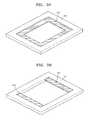
- the patterning slit sheet 151 in one embodiment, is combined with the frame 154 .
- the frame 154 is formed in a lattice shape, similar to a window frame.
- the frame 154 may be combined with one surface of the non-slit region 153 of the patterning slit sheet 151 .
- the frame 154 and the patterning slit sheet 151 are combined in such a manner that a predetermined tensile force is applied to the patterning slit sheet 151 .
- a degree of pattern precision of the patterning slit sheet 151 during a deposition process may be affected by a manufacturing error and/or a thermal expansion error of the patterning slit sheet 151 .
- a counterforce technique may be used to minimize or reduce a manufacturing error of the patterning slit sheet 151 . This is described according to one embodiment in further detail below. First, a tensile force is applied to the patterning slit sheet 151 by applying pressure to the patterning slit sheet 151 from the inside to the outside thereof.
- a compression force is applied to the frame 154 in an opposite direction to the direction in which the external tensile force is applied to the patterning slit sheet 151 , such that the compression force is in equilibrium with the external tensile force applied to the patterning slit sheet 151 .
- the frame 154 and the patterning slit sheet 151 are combined, such as by welding, for example.
- the external tensile force applied to the patterning slit sheet 151 which is in equilibrium with the compression force applied to the frame 154 , is removed so as to apply the tensile force to the patterning slit sheet 151 via the frame 154 .
- the patterning slit sheet 151 may be manufactured with a manufacturing error of 2 ⁇ m or less.
- a tensile force may be applied to the patterning slit sheet 151 , such as to a predetermined degree or greater such that the patterning slit sheet 151 may be prevented or substantially prevented from being deformed (e.g., sagging) during the deposition process, and a compression force may be applied to the frame 154 , such as to a predetermined degree or greater.
- a compression force may be applied to the frame 154 to the predetermined degree or greater, the frame is likely to be deformed.
- a greater tensile force should be applied to the patterning slit sheet 151 and a compression force applied to the frame 154 should also be increased to correspond to the greater tensile force.
- the frame 154 to which the greater compression force is applied may bend, and a manufacturing process is not easy to perform when the weight of the frame 154 is significantly increased to prevent the frame from bending.
- the slit unit 152 of the patterning slit sheet 151 is formed to be larger than a deposition area on which a deposition process is to be performed, and the above-described problem is avoided.
- a deposition area DA is disposed between non-deposition areas NA on the substrate 500 .
- the deposition material in the deposition source 110 passes through the patterning slit sheet 151 and reaches the deposition area DA on the substrate 500 to perform a deposition process.
- the slit unit 152 overlaps with the deposition area DA and is larger than the deposition area DA. That is, the slit unit 152 partially overlaps with the non-deposition areas NA.
- the non-slit region 153 is smaller and the region of the slit unit 152 having the plurality of slits is wider. If a tensile force of the same degree is applied to the patterning slit sheet 151 , the larger the slit unit 152 , the higher degree to which the patterning slit sheet 151 may be tensile-strained due to the plurality of slits that pass through the patterning slit sheet 151 . In other words, a degree to which the patterning slit sheet 151 is tensile-strained is high when the slit unit 152 is large, provided the tensile force of the same degree is applied.
- the larger the slit unit 152 the less the tensile force that may be applied to the patterning slit sheet 151 . Accordingly, a compression force applied to the frame 154 may be lessened. Thus, the frame 154 is prevented or substantially prevented from being deformed and the thickness of the frame 154 does not need to be increased, thereby facilitating the manufacturing process.
- the shielding unit 155 in one embodiment, is formed on inner side surfaces of the frame 154 .
- the shielding unit 155 may be formed covering inner side surfaces of the frame 154 , as illustrated in FIG. 3A , or a shielding unit 155 ′ may be formed on two inner side surfaces that face each other from among the inner side surfaces of the frame 154 , as illustrated in FIG. 3B .
- the structure of the shielding unit 155 may vary according to shapes and sizes of the substrate 500 which is a target deposition substrate, the patterning slit sheet 151 , and the frame 154 .
- the shielding unit 155 overlaps with the non-deposition areas NA and corresponds to edge portions of the deposition area DA, as illustrated in FIG. 1 . Since the slit unit 152 is larger than the deposition area DA, as described above, the deposition material in the deposition source 110 may be deposited not only on the deposition area DA but also on the non-deposition areas NA. In this case, an organic layer is not likely to be formed in a desired pattern. However, this is prevented or substantially prevented by the shielding unit 155 . In other words, the shielding unit 155 allows the deposition material in the deposition source 110 to be deposited only on the deposition area DA.
- the patterning slit sheet assembly 150 applies a tensile force to the patterning slit sheet 151 when the frame 154 and the patterning slit sheet 151 are combined with each other, thereby minimizing or reducing a manufacturing error of the patterning slit sheet 151 and preventing or substantially preventing the patterning slit sheet 151 from being deformed. Accordingly, a deposition process may be performed to deposit a thin film in a fine pattern on a substrate 500 .
- the slit unit 152 of the patterning slit sheet 151 may be formed to be large, and particularly, to be larger than the deposition area DA, a tensile force applied to the patterning slit sheet 151 is reduced to lessen a compression force to be applied to the frame 154 , thereby preventing or substantially preventing the frame 154 from being deformed.
- the shielding unit 155 is formed on the frame 154 such that the deposition material may not be deposited on the non-deposition areas NA, but on the deposition area DA, thereby increasing the efficiency of the deposition process to deposit a thin film in a fine pattern.
- FIG. 4 is a schematic perspective view of an organic layer deposition apparatus 100 according to an embodiment of the present invention
- FIG. 5 is a schematic side sectional view of the organic layer deposition apparatus 100
- FIG. 6 is a schematic front sectional view of the organic layer deposition apparatus 100 .
- the organic layer deposition apparatus 100 includes a deposition source 110 , a deposition source nozzle unit 120 , and the patterning slit sheet assembly 150 .
- a deposition material 115 discharged from the deposition source 110 passes through the deposition source nozzle unit 120 and the patterning slit sheet assembly 150 and is then deposited onto the substrate 500 in a desired pattern.
- a deposition process that uses the organic layer deposition apparatus 100 may be performed in a chamber that is maintained in a high vacuum.
- the temperature of the patterning slit sheet 151 is sufficiently lower than that of the deposition source 110 .
- the temperature of the patterning slit sheet 151 may be about 100° C. or less.
- the temperature of the patterning slit sheet 151 should be sufficiently low so as to minimize or reduce thermal expansion of the patterning slit sheet 151 .
- the substrate 500 may be a substrate for flat panel displays, for example.
- a large substrate such as a mother glass, for manufacturing a plurality of flat panel displays, may be used as the substrate 500 .
- other substrates may be used.
- deposition is performed while the substrate 500 is moved relative to the organic layer deposition apparatus 100 .
- the substrate 500 may be disposed on an electrostatic chuck 600 and may be then transferred.
- the size of an FMM is equal to the size of a substrate.
- the size of the FMM has to be increased as the substrate becomes larger, it is neither straightforward to manufacture a large FMM nor to extend an FMM to be accurately aligned with a pattern.
- deposition may be performed while the organic layer deposition apparatus 100 or the substrate 500 is moved relative to the other.
- deposition may be continuously performed while the substrate 500 , which is disposed such as to face the organic layer deposition apparatus 100 , is moved in a Y-axis direction. That is, deposition may be performed in a scanning manner while the substrate 500 is moved in a direction indicated by the arrow “A” in FIGS. 4 and 5 .
- the patterning slit sheet 151 may be significantly smaller than an FMM used in a conventional deposition method.
- deposition is continuously performed (e.g., in a scanning manner) while the substrate 500 is moved in the Y-axis direction.
- the length of the patterning slit sheet 151 in at least one of the X-axis or the Y-axis directions may be significantly less than the length of the substrate 500 in at least one of the X-axis or the Y-axis directions.
- the patterning slit sheet 151 may be formed to be significantly smaller than a FMM used in a conventional deposition method, it is relatively easy to manufacture the patterning slit sheet 151 according to embodiments of the present invention.
- using the patterning slit sheet 151 which is smaller than the FMM used in the conventional deposition method, is more convenient in other processes, including etching and other subsequent processes, such as precise extension, welding, moving, and cleaning processes, compared to the conventional deposition method using the larger FMM. This is especially advantageous for a relatively large display device.
- the deposition source 110 that contains and heats the deposition material 115 is disposed at a side facing the substrate 500 .
- the deposition material 115 is vaporized in the deposition source 110 and deposited on the substrate 500 .
- the deposition source 110 includes a crucible 112 filled with the deposition material 115 , and a cooling block 111 that heats the crucible 112 to vaporize the deposition material 115 in the crucible 112 toward a side of the crucible 112 , and in particular, toward the deposition source nozzle unit 120 .
- the cooling block 111 prevents or substantially prevents radiation of heat from the crucible 112 to the outside.
- the cooling block 111 may include a heater (not shown) that heats the crucible 112 .
- the deposition source nozzle unit 120 is disposed at a side of the deposition source 110 , and in particular, at the side of the deposition source 110 facing the substrate 500 .
- the deposition source nozzle unit 120 includes a plurality of deposition source nozzles 121 arranged at intervals (e.g., equal intervals) in the Y-axis direction (e.g., a scanning direction of the substrate 500 ).
- the deposition material 115 that is vaporized in the deposition source 110 passes through the deposition source nozzle unit 120 toward the substrate 500 .
- the deposition source nozzle unit 120 includes the plurality of deposition source nozzles 121 arranged in the Y-axis direction (e.g., the scanning direction of the substrate 500 ), and the size of a pattern formed of the deposition material 115 discharged through the slit unit 152 of the patterning slit sheet 151 is affected by the size of the deposition source nozzles 121 (since there may be only one line of the deposition source nozzles 121 in the X-axis direction). Thus, no shadow zone may be formed on the substrate 500 .
- the plurality of deposition source nozzles 121 are arranged in the scanning direction of the substrate 500 , even if there is a difference in flux between the plurality of deposition source nozzles 121 , the difference may be compensated for and deposition uniformity may be maintained constant.
- the patterning slit sheet assembly 150 that includes the patterning slit sheet 151 , the frame 154 , and the shielding unit 155 , is disposed between the deposition source 110 and the substrate 500 .
- the patterning slit sheet 151 includes the slit unit 152 and the non-slit region 153 .
- the plurality of slits are formed in an X-axis direction.
- the deposition material 115 that is vaporized in the deposition source 110 passes through the deposition source nozzle unit 120 and the patterning slit sheet 151 , and particularly, the slit unit 152 , toward the substrate 500 .
- the structure of the patterning slit sheet assembly 150 that includes the patterning slit sheet 151 , the frame 154 , and the shielding unit 155 , may be the same as described above with respect to FIGS. 1 through 3B , and thus further description thereof will not be repeated here.
- the deposition source 110 and the deposition source nozzle unit 120 coupled to the deposition source 110 may be disposed apart from the patterning slit sheet assembly 150 by a predetermined distance.
- the deposition source 110 and the deposition source nozzle unit 120 coupled to the deposition source 110 may be connected to the patterning slit sheet assembly 150 by connection members 135 .
- the deposition source 110 , the deposition source nozzle unit 120 , and the patterning slit sheet assembly 150 may be integrally formed as one body by being connected to each other via the connection members 135 .
- the connection members 135 may guide the deposition material 115 , which is discharged through the deposition source nozzles 121 , to move straight and to not flow in the X-axis direction.
- connection members 135 are formed only on left and right sides of the deposition source 110 , the deposition source nozzle unit 120 , and the patterning slit sheet assembly 150 to guide the deposition material 115 to not flow in the X-axis direction; however, aspects of the present invention are not limited thereto.
- the connection member 135 may be formed in the configuration of a sealed box to guide flow of the deposition material 115 in both the X-axis and Y-axis directions.
- the organic layer deposition apparatus 100 performs deposition while being moved relative to the substrate 500 .
- the patterning slit sheet assembly 150 is separated from the substrate 500 by a predetermined distance.
- the conventional deposition method using a FMM deposition is performed with the FMM in close contact with a substrate in order to prevent formation of a shadow zone on the substrate.
- the contact may cause defects.
- the size of the mask has to be the same as the size of the substrate since the mask cannot be moved relative to the substrate.
- the size of the mask has to be increased as display devices become larger.
- the patterning slit sheet assembly 150 is disposed to be separated from the substrate 500 by a predetermined distance. Thus, it is possible to prevent or substantially prevent defects from occurring when the patterning slit sheet assembly 150 contacts the substrate 500 during the deposition process.
- the patterning slit sheet assembly 150 since the patterning slit sheet assembly 150 , and particularly, the pattering slit sheet 151 is formed to be smaller than the substrate 500 , the patterning slit sheet assembly 150 may be easily manufactured.
- FIG. 7 is a schematic perspective view of an organic layer deposition apparatus 100 ′ according to another embodiment of the present invention.
- the organic layer deposition apparatus 100 ′ includes the deposition source 110 , a deposition source nozzle unit 120 ′, and the patterning slit sheet assembly 150 .
- the deposition source 110 in one embodiment, includes the crucible 112 filled with the deposition material 115 , and the cooling block 111 that heats the crucible 112 to vaporize the deposition material 115 in the crucible 112 toward the deposition source nozzle unit 120 ′.
- the deposition source nozzle unit 120 ′ is disposed at a side of the deposition source 110 .
- the deposition source nozzle unit 120 ′ includes a plurality of deposition source nozzles 121 ′ arranged in the Y-axis direction.
- the patterning slit sheet assembly 150 is disposed between the deposition source 110 and the substrate 500 .
- the deposition source 110 and the deposition source nozzle unit 120 ′ may be connected to the patterning slit sheet assembly 150 by the connection members 135 .
- the structure of the patterning slit sheet assembly 150 that includes the patterning slit sheet 151 , the frame 154 , and the shielding unit 155 , may be the same as that of embodiments described above, and thus further description thereof will not be repeated here.
- the plurality of deposition source nozzles 121 ′ formed in the deposition source nozzle unit 120 ′ are tilted at a predetermined angle, unlike in the deposition source nozzle unit 120 described above with reference to FIGS. 4 through 6 .
- the deposition source nozzles 121 ′ may include deposition source nozzles 121 a and 121 b arranged in two rows.
- the deposition source nozzles 121 a and 121 b may be arranged in two rows to alternate in a zigzag pattern.
- the deposition source nozzles 121 a and 121 b may be tilted at a predetermined angle on an X-Z plane.
- the deposition source nozzles 121 a and 121 b are arranged to be tilted at a predetermined angle. In one embodiment, the deposition source nozzles 121 a in a first row and the deposition source nozzles 121 b in a second row may be tilted to face each other.
- the deposition of the deposition material 115 may be adjusted to lessen a thickness variation between the center and the end portions of an organic layer on the substrate 500 and improve thickness uniformity of the organic layer. Moreover, utilization efficiency of the deposition material 115 may also be improved.
- FIG. 8 is a schematic perspective view of an organic layer deposition apparatus according to another embodiment of the present invention.
- the organic layer deposition apparatus may include a plurality of organic layer deposition apparatuses, such as first, second, and third deposition apparatuses 100 , 200 , and 300 , each of which may have a same structure as the organic layer deposition apparatus 100 illustrated in FIGS. 4 through 6 .
- the organic layer deposition apparatus according to the embodiment shown in FIG. 8 may include a multi-deposition source unit that consists of a plurality of deposition sources and that concurrently (e.g., simultaneously) discharge different deposition materials, such as for respectively forming a red (R) emission layer, a green (G) emission layer, and a blue (B) emission layer.
- the organic layer deposition apparatus includes the first organic layer deposition apparatus 100 , the second organic layer deposition apparatus 200 , and the third organic layer deposition apparatus 300 .
- Each of the first to third organic layer deposition apparatuses 100 , 200 , 300 may have the same structure as the organic layer deposition apparatus 100 described with reference to FIGS. 4 through 6 , and thus a detailed description thereof will not be repeated here.
- the structure of the patterning slit sheet assembly 150 that includes the patterning slit sheet 151 , the frame 154 , and the shielding unit 155 may be the same as that of the organic layer deposition apparatus 100 described above, and thus further description thereof will not be repeated here.
- the deposition sources of the first organic layer deposition apparatus 100 , the second organic layer deposition apparatus 200 , and the third organic layer deposition apparatus 300 may contain different deposition materials, respectively.
- the first organic layer deposition apparatus 100 may contain a deposition material for forming a red (R) emission layer
- the second organic layer deposition apparatus 200 may contain a deposition material for forming a green (G) emission layer
- the third organic layer deposition apparatus 300 may contain a deposition material for forming a blue (B) emission layer.
- the red (R) emission layer, the green (G) emission layer, and the blue (B) emission layer may be concurrently (e.g., simultaneously) formed by using the multi-deposition source unit.
- a time needed to manufacture an organic light emitting display device may be significantly reduced.
- the organic light emitting display device may be manufactured using a reduced number of chambers, such that equipment costs may also be significantly reduced.
- the patterning slit sheet assemblies 150 of the first organic layer deposition apparatus 100 , the second organic layer deposition apparatus 200 , and the third organic layer deposition apparatus 300 may be arranged to be offset by a distance (e.g., a constant distance) with respect to each other, thereby preventing or substantially preventing deposition regions corresponding to the patterning slit sheets 150 from overlapping with one another on a substrate 500 .
- a distance e.g., a constant distance
- the first organic layer deposition apparatus 100 , the second organic layer deposition apparatus 200 , and the third organic layer deposition apparatus 300 are used to respectively deposit the R emission layer, the G emission layer, and the B emission layer, then a plurality of slits of the slit unit 152 of the patterning slit sheet 151 of the first organic layer deposition apparatus 100 , a plurality of slits of the slit unit 152 of the patterning slit sheet 151 of the second organic layer deposition apparatus 200 , and a plurality of slits of the slit unit 152 of the patterning slit sheet 151 of the third organic layer deposition apparatus 300 may be arranged to not be aligned with respect to one another, to respectively form the R emission layer, the G emission layer, and the B emission layer in different regions of the substrate 500 .
- an organic layer deposition apparatus includes the three organic layer deposition apparatuses 100 , 200 , 300
- embodiments of the present invention are not limited thereto.
- an organic layer deposition apparatus may include a plurality of organic layer deposition apparatuses, each of which contains a different deposition material.
- an organic layer deposition apparatus may include five organic layer deposition apparatuses respectively containing materials for an R emission layer, a G emission layer, a B emission layer, an auxiliary R′ layer of the R emission layer, and an auxiliary G′ layer of the G emission layer.
- the substrate 500 may be moved relative to the organic layer deposition apparatus 400 .
- the substrate 500 may be moved in a direction of the arrow “A” relative to the organic layer deposition apparatus 400 .
- the patterning slit sheet assembly 150 may be significantly smaller than a FMM used in a conventional deposition method.
- deposition is continuously performed (e.g., in a scanning manner) while the substrate 500 is moved (e.g., in the Y-axis direction).
- a length of the patterning slit sheet 151 may be significantly less than a length of the substrate 500 , and a width of the patterning slit sheet 151 (e.g., in the X-axis direction) and a width of the substrate 500 (e.g., in the X-axis direction) may be substantially equal to each other.
- the width of the patterning slit sheet 151 in the X-axis direction may be less than the width of the substrate 500 in the X-axis direction, and deposition may be performed on the entire substrate 500 in the scanning manner while the substrate 500 or the organic layer deposition apparatus 400 is moved relative to the other.
- the patterning slit sheet 151 may be formed to be significantly smaller than a FMM used in a conventional deposition method, it is relatively easy to manufacture the patterning slit sheet 151 according to embodiments of the present invention.
- the deposition source 110 that contains and heats the deposition material 115 is disposed at a side facing the substrate 500 .
- the deposition source 110 includes the crucible 112 filled with the deposition material 115 , and the cooling block 111 surrounding the crucible 112 .
- the cooling block 111 prevents or substantially prevents radiation of heat from the crucible 112 to the outside.
- the cooling block 111 may include a heater (not shown) that heats the crucible 112 .
- the deposition source nozzle unit 420 is disposed at a side of the deposition source 110 , and in particular, at the side of the deposition source 110 facing the substrate 500 .
- the deposition source nozzle unit 420 includes a plurality of deposition source nozzles 421 that may be arranged at intervals (e.g., equal intervals) in the X-axis direction.
- the deposition material 115 that is vaporized in the deposition source 110 passes through the deposition source nozzles 421 of the deposition source nozzle unit 420 toward the substrate 500 that is a deposition target substrate.
- the plurality of barrier plates 131 arranged as described above partition a deposition space between the deposition source nozzle unit 420 and the patterning slit sheet assembly 150 into a plurality of sub-deposition spaces S.
- the deposition space is divided by the barrier plates 131 into the sub-deposition spaces S that respectively correspond to the deposition source nozzles 421 through which the deposition material 115 is discharged.
- the barrier plates 131 may be respectively disposed between adjacent deposition source nozzles 421 .
- each of the deposition source nozzles 421 may be disposed between two adjacent barrier plates 131 .
- the deposition source nozzles 421 may be respectively located at the midpoints between pairs of adjacent barrier plates 131 .
- the present invention is not limited to this structure.
- a plurality of deposition source nozzles 421 may be disposed between two adjacent barrier plates 131 , and the deposition source nozzles 421 may be respectively located at the midpoint between the two adjacent barrier plates 131 .
- the barrier plates 131 partition the space between the deposition source nozzle unit 420 and the patterning slit sheet assembly 150 into the plurality of sub-deposition spaces S as described above, the deposition material 115 discharged through each of the deposition source nozzles 421 is not mixed with the deposition material 115 discharged through the other deposition source nozzles 421 , passes through the slit unit 152 of the patterning slit sheet assembly 150 , and is then deposited on the substrate 500 .
- the barrier plates 131 guide the deposition material 115 , which is discharged through the deposition source nozzles 421 , to move straight (i.e. flow in the Z-axis direction).
- the deposition source nozzle unit 420 and the barrier plate assembly 130 may be separated from each other by a predetermined distance. This may prevent or substantially prevent heat radiated from the deposition source unit 110 from being conducted to the barrier plate assembly 130 .
- embodiments of the present invention are not limited thereto.
- an appropriate heat insulator (not shown) may be disposed between the deposition source nozzle unit 420 and the barrier plate assembly 130 , and the deposition source nozzle unit 420 and the barrier plate assembly 130 may be bound together with the heat insulator therebetween.
- the barrier plate assembly 130 may be constructed to be detachable from the organic layer deposition apparatus 400 .
- the deposition space may be enclosed by using the barrier plate assembly 130 , such that the deposition material 115 that remains undeposited is mostly deposited within the barrier plate assembly 130 .
- the barrier plate assembly 130 may be constructed to be detachable from the organic layer deposition apparatus 400 , when a large amount of the deposition material 115 lies in the barrier plate assembly 130 after a long deposition process, the barrier plate assembly 130 may be detached from the organic layer deposition apparatus 400 and then placed in a separate deposition material recycling apparatus in order to recover the deposition material 115 . Due to the structure of the organic layer deposition apparatus 400 according to such an embodiment, a reuse rate of the deposition material 115 is increased, such that the deposition efficiency is improved and the manufacturing costs are reduced.
- the patterning slit sheet assembly 150 is disposed between the deposition source 110 and the substrate 500 .
- the frame 154 has a shape similar to a window frame, and is combined with the patterning slit sheet 151 .
- the patterning slit sheet 151 includes the slit unit 152 and the non-slit region 153 .
- a plurality of slits are formed in the X-axis direction and extend in the Y-axis direction.
- the structure of the patterning slit sheet assembly 150 that includes the patterning slit sheet 151 , the frame 154 , and the shielding unit 155 may be the same as described above with respect to the previously described embodiments, and thus further description will not be repeated here.
- the total number of the plurality of slits of the slit unit 152 may be greater than that of the deposition source nozzles 421 . Further, the total number of the plurality of slits of the slit unit 152 disposed between two adjacent barrier plates 131 may be greater than the total number of deposition source nozzles 421 disposed between two adjacent barrier plates 131 . The number of the plurality of slits of the slit unit 152 may be equal to that of deposition patterns to be formed on the substrate 500 .
- the barrier plate assembly 130 and the patterning slit sheet assembly 150 may be disposed to be separated from each other by a predetermined distance, and may be connected by connection members 133 .
- the temperature of the barrier plate assembly 130 may increase to 100° C. or greater due to the deposition source 110 having a high temperature. Therefore, the barrier plate assembly 130 and the patterning slit sheet assembly 150 may be separated from each other by the predetermined distance in order to prevent or substantially prevent the heat of the barrier plate assembly 130 from being conducted to the patterning slit sheet assembly 150 .
- the patterning slit sheet assembly 150 since the patterning slit sheet assembly 150 , and particularly, the pattering slit sheet 151 , is formed to be smaller than the substrate 500 , the patterning slit sheet assembly 150 may be easily manufactured.
- the substrate 500 which is a deposition target substrate, is disposed in the chamber.
- the deposition source 110 that contains and heats the deposition material 115 is disposed at an opposite side of the chamber to a side at which the substrate 500 is disposed.
- the structure of the deposition source 110 may be the same as that of the organic layer deposition apparatus 100 described above with reference to FIGS. 4 through 6 , and thus a detailed description thereof will not be repeated here.
- the first barrier plate assembly 130 may also be configured the same as that of the organic layer deposition apparatus 400 described above and shown in FIGS. 9 through 11 , and thus a detailed description thereof will not be repeated here.
- the patterning slit sheet assembly 150 of the organic layer deposition apparatus 400 ′ includes the patterning slit sheet 151 , the frame 154 , and the shielding unit 155 , and may have the same structure as described above, and thus further description will not be repeated here.
- the second barrier plate assembly 140 is disposed at a side of the first barrier plate assembly 130 .
- the second barrier plate assembly 140 includes a plurality of second barrier plates 141 and a second barrier plate frame 142 that covers sides of the second barrier plates 141 .
- the second barrier plates 141 may be arranged parallel to each other at intervals (e.g., equal intervals) in the X-axis direction.
- Each of the plurality of second barrier plates 141 may be formed to extend in a Y-Z plane in FIG. 12 (i.e. perpendicular to the X-axis direction).
- the plurality of second barrier plates 141 may be disposed to respectively correspond to the plurality of first barrier plates 131 .
- the plurality of second barrier plates 141 may be aligned with respect to the plurality of first barrier plates 131 , respectively. That is, each pair of the corresponding first and second barrier plates 131 and 141 may be located on the same plane.
- the first barrier plates 131 and the second barrier plates 141 respectively have the same thickness in the X-axis direction, but embodiments of the present invention are not limited thereto.
- a plurality of the organic layer deposition apparatuses 400 ′ may be consecutively arranged, as described above with respect to the embodiment shown in FIG. 8 .
- the active layer 41 is formed in a pattern (e.g., a predetermined pattern) on the buffer layer 31 .
- the active layer 41 may include a p-type or n-type semiconductor material.
- a gate insulating layer 32 is formed on the active layer 41 .
- the gate electrode 42 is formed on a region of the gate insulating layer 32 corresponding to the active layer 41 .
- An interlayer insulating layer 33 is formed covering the gate electrode 42 , and the source/drain electrode 43 may be disposed on the interlayer insulating layer 43 to contact a predetermined region of the active layer 41 .
- a passivation layer 34 is formed covering the source/drain electrode 43 , and an additional insulating layer may be formed on the passivation layer 34 to planarize the passivation layer 34 .
- the first electrode 61 is formed on the passivation layer 34 .
- the first electrode 61 is electrically connected to the drain electrode 43 .
- a pixel defining layer 35 is formed covering the first electrode 61 .
- An opening 64 is formed in the pixel defining layer 35 , and the intermediate layer 63 including an organic emission layer (not shown) is formed in a region defined by the opening 64 .
- the second electrode 62 is formed on the intermediate layer 63 .
- the intermediate layer 63 including the organic emission layer may be formed by using a patterning slit sheet assembly and an organic layer deposition apparatus according to embodiments of the present invention, such as the patterning slit sheet assembly 150 and the organic layer deposition apparatus 100 including the patterning slit sheet assembly 150 described above and shown in FIG. 4 .
- the substrate 30 is transferred into a chamber (not shown). Then, a deposition process is performed using a desired deposition material to form the intermediate layer 63 in a desired pattern.
- the organic layer deposition apparatuses according to the above-described embodiments of the present invention may be applied to form an organic or inorganic layer of an organic TFT, for example, and to form layers from various materials.
Landscapes
- Chemical & Material Sciences (AREA)
- Engineering & Computer Science (AREA)
- Chemical Kinetics & Catalysis (AREA)
- Materials Engineering (AREA)
- Mechanical Engineering (AREA)
- Metallurgy (AREA)
- Organic Chemistry (AREA)
- Manufacturing & Machinery (AREA)
- Electroluminescent Light Sources (AREA)
- Physical Vapour Deposition (AREA)
Abstract
Description
Claims (10)
Applications Claiming Priority (2)
| Application Number | Priority Date | Filing Date | Title |
|---|---|---|---|
| KR10-2011-0050842 | 2011-05-27 | ||
| KR1020110050842A KR101857249B1 (en) | 2011-05-27 | 2011-05-27 | Patterning slit sheet assembly, apparatus for organic layer deposition, method for manufacturing organic light emitting display apparatus and organic light emitting display apparatus |
Publications (2)
| Publication Number | Publication Date |
|---|---|
| US20120298970A1 US20120298970A1 (en) | 2012-11-29 |
| US8906731B2 true US8906731B2 (en) | 2014-12-09 |
Family
ID=47218627
Family Applications (1)
| Application Number | Title | Priority Date | Filing Date |
|---|---|---|---|
| US13/461,669 Expired - Fee Related US8906731B2 (en) | 2011-05-27 | 2012-05-01 | Patterning slit sheet assembly, organic layer deposition apparatus, method of manufacturing organic light-emitting display apparatus, and the organic light-emitting display apparatus |
Country Status (2)
| Country | Link |
|---|---|
| US (1) | US8906731B2 (en) |
| KR (1) | KR101857249B1 (en) |
Families Citing this family (7)
| Publication number | Priority date | Publication date | Assignee | Title |
|---|---|---|---|---|
| US8882920B2 (en) * | 2009-06-05 | 2014-11-11 | Samsung Display Co., Ltd. | Thin film deposition apparatus |
| US8876975B2 (en) | 2009-10-19 | 2014-11-04 | Samsung Display Co., Ltd. | Thin film deposition apparatus |
| KR101406199B1 (en) * | 2012-12-27 | 2014-06-12 | 주식회사 선익시스템 | Apparatus for deposition |
| KR102363252B1 (en) | 2014-11-12 | 2022-02-16 | 삼성디스플레이 주식회사 | Thin film deposition apparatus, method of manufacturing organic light-emitting display device by using the same and organic light-emitting display device |
| US20200002801A1 (en) * | 2017-09-28 | 2020-01-02 | Sharp Kabushiki Kaisha | Vapor deposition mask and manufacturing method for vapor deposition mask |
| US11614012B2 (en) * | 2017-12-05 | 2023-03-28 | Cymer, Llc | Nonwoven screens for dust trapping in laser discharge chambers |
| KR102190638B1 (en) * | 2018-09-10 | 2020-12-14 | 주식회사 에스에프에이 | Display glass deposition system |
Citations (481)
| Publication number | Priority date | Publication date | Assignee | Title |
|---|---|---|---|---|
| JPS57194252U (en) | 1981-06-02 | 1982-12-09 | ||
| US4416217A (en) | 1981-07-31 | 1983-11-22 | Ulvac Seimaku Kabushiki Kaisha | Apparatus for forming an inhomogeneous optical layer |
| US4468648A (en) | 1982-10-15 | 1984-08-28 | Mamoru Uchikune | Switchable permanent magnetic chuck |
| US4687939A (en) | 1983-11-07 | 1987-08-18 | Hitachi, Ltd. | Method and apparatus for forming film by ion beam |
| US4792378A (en) | 1987-12-15 | 1988-12-20 | Texas Instruments Incorporated | Gas dispersion disk for use in plasma enhanced chemical vapor deposition reactor |
| US4901667A (en) | 1985-08-09 | 1990-02-20 | Hitachi, Ltd. | Surface treatment apparatus |
| JPH02247372A (en) | 1989-03-17 | 1990-10-03 | Mitsubishi Electric Corp | Thin film formation |
| JPH04272170A (en) | 1991-02-25 | 1992-09-28 | Tokai Carbon Co Ltd | Graphite crucible for vacuum vapor deposition |
| JPH0598425A (en) | 1991-10-04 | 1993-04-20 | Mitsubishi Electric Corp | Thin film forming device |
| JPH0522405Y2 (en) | 1985-12-05 | 1993-06-08 | ||
| JPH05230628A (en) | 1992-02-18 | 1993-09-07 | Fujitsu Ltd | Metal film forming device and metal recovery method in metal film forming device |
| US5454847A (en) | 1992-09-18 | 1995-10-03 | Alcatel Alsthom Compagnie Generale D'electricite | Vapor deposition method for depositing a film of fluorine-containing glass on a substrate |
| US5460654A (en) | 1992-07-01 | 1995-10-24 | Fujitsu Limited | Apparatus for generating raw material gas used in apparatus for growing thin film |
| US5487609A (en) | 1991-05-13 | 1996-01-30 | Thk Co., Ltd. | Slide unit for linear motion |
| JPH0827568B2 (en) | 1990-07-02 | 1996-03-21 | 三田工業株式会社 | Transfer paper separating device in image forming apparatus |
| JPH0995776A (en) | 1995-09-29 | 1997-04-08 | Sony Corp | Vacuum deposition device |
| JPH1050478A (en) | 1996-04-19 | 1998-02-20 | Toray Ind Inc | Organic field emission element and manufacture thereof |
| US5742129A (en) | 1995-02-21 | 1998-04-21 | Pioneer Electronic Corporation | Organic electroluminescent display panel with projecting ramparts and method for manufacturing the same |
| JPH10120171A (en) | 1996-10-15 | 1998-05-12 | Balzers Ag | Device for conveying base plate in vacuum treatment system |
| JPH10270535A (en) | 1997-03-25 | 1998-10-09 | Nikon Corp | Moving stage device and circuit-device manufacture using the same |
| WO1999025894A1 (en) | 1997-11-17 | 1999-05-27 | The Trustees Of Princeton University | Low pressure vapor phase deposition of organic thin films |
| JPH11144865A (en) | 1997-11-05 | 1999-05-28 | Casio Comput Co Ltd | Manufacture of organic electroluminescent element |
| JP2000068054A (en) | 1998-08-26 | 2000-03-03 | Hokuriku Electric Ind Co Ltd | Manufacture of el element |
| US6045671A (en) | 1994-10-18 | 2000-04-04 | Symyx Technologies, Inc. | Systems and methods for the combinatorial synthesis of novel materials |
| KR20000023929A (en) | 1999-10-29 | 2000-05-06 | 최중호 | Apparatus and method for emitting odor |
| KR100257219B1 (en) | 1997-10-23 | 2000-05-15 | 박용관 | Method and device for making a safety operation of a polyethylene gas pipe valve arrangement |
| US6091195A (en) | 1997-02-03 | 2000-07-18 | The Trustees Of Princeton University | Displays having mesa pixel configuration |
| US6099649A (en) | 1997-12-23 | 2000-08-08 | Applied Materials, Inc. | Chemical vapor deposition hot-trap for unreacted precursor conversion and effluent removal |
| JP2000282219A (en) | 1999-04-02 | 2000-10-10 | Canon Inc | Method for reproducing mask for organic film vacuum deposition and device therefor |
| KR20000019254U (en) | 1999-04-07 | 2000-11-06 | 손대균 | Roundin WheeL |
| JP2000323277A (en) | 1999-05-12 | 2000-11-24 | Pioneer Electronic Corp | Organic electroluminescent multi-color display and its manufacture |
| JP2001028325A (en) | 1999-07-13 | 2001-01-30 | Tdk Corp | Method and device for transfer chip part, and electrode- forming device |
| JP2001052862A (en) | 1999-08-04 | 2001-02-23 | Hokuriku Electric Ind Co Ltd | Manufacture of organic el element and device therefor |
| JP2001093667A (en) | 1999-09-28 | 2001-04-06 | Sanyo Electric Co Ltd | Organic light-emitting element, device and method for manufacturing the same |
| KR20010030175A (en) | 1999-09-01 | 2001-04-16 | 이데이 노부유끼 | Plane display unit and plane display apparatus |
| KR20010039298A (en) | 1999-10-29 | 2001-05-15 | 김영남 | Field emission display |
| US20010004186A1 (en) | 1999-12-10 | 2001-06-21 | Song Gi-Young | Shadow mask frame assembly for flat CRT |
| US20010006827A1 (en) | 1999-12-27 | 2001-07-05 | Semiconductor Energy Laboratory Co., Ltd. | Film formation apparatus and method for forming a film |
| KR20010059939A (en) | 1999-12-30 | 2001-07-06 | 송문섭 | Mobile station for mobile communication system |
| US6274198B1 (en) | 1997-02-24 | 2001-08-14 | Agere Systems Optoelectronics Guardian Corp. | Shadow mask deposition |
| US6280821B1 (en) | 1998-09-10 | 2001-08-28 | Ppg Industries Ohio, Inc. | Reusable mask and method for coating substrate |
| US20010019807A1 (en) | 1999-12-24 | 2001-09-06 | Tsutomu Yamada | Deposition mask and manufacturing method thereof, and electroluminescence display device and manufacturing method thereof |
| US20010026638A1 (en) | 2000-03-28 | 2001-10-04 | Katsuya Sangu | Positioning apparatus used in a process for producing multi-layered printed circuit board and method of using the same |
| US20010034175A1 (en) | 2000-02-16 | 2001-10-25 | Toshihiko Miyazaki | Method and apparatus for manufacturing image displaying apparatus |
| KR20010092914A (en) | 2000-03-27 | 2001-10-27 | 윤종용 | Electrical static chuck comprising a shadow ring |
| KR20020000201A (en) | 2000-06-23 | 2002-01-05 | 최승락 | Method cleaning Liquid Chrystal Display using Laser and Vapor Phase |
| KR20020001555A (en) | 2000-06-22 | 2002-01-09 | 키도 준지 | Apparatus for and method of vacuum vapor deposition and organic electroluminescent device |
| US20020011785A1 (en) | 1998-11-18 | 2002-01-31 | Ching W. Tang | A full color active matrix organic electroluminescent display panel having an integrated shadow mask |
| JP2002075638A (en) | 2000-08-29 | 2002-03-15 | Nec Corp | Vapor deposition method of mask and vapor deposition device |
| US20020033136A1 (en) | 1999-04-02 | 2002-03-21 | Silicon Valley Group, Thermal Systems Llc. | Semiconductor wafer processing system with vertically-stacked process chambers and single-axis dual-wafer transfer system |
| US20020036759A1 (en) | 2000-09-25 | 2002-03-28 | Masaru Ise | Automatic exposing apparatus for both sides and exposing method thereof for works |
| KR20020025760A (en) | 2000-09-28 | 2002-04-04 | 다카노 야스아키 | Method of attaching layer material and forming layer in predetermined pattern on substrate using mask |
| US6371451B1 (en) | 1999-10-29 | 2002-04-16 | Korea Institute Of Science And Technology | Scent diffusion apparatus and method |
| US20020050061A1 (en) | 2000-06-29 | 2002-05-02 | Daido Komyoji | Method and apparatus for forming pattern onto panel substrate |
| KR20020050922A (en) | 2000-12-22 | 2002-06-28 | 박종섭 | Virtual channel sdram |
| US6417034B2 (en) | 2000-05-01 | 2002-07-09 | Nec Corporation | Manufacturing method for organic EL device |
| US20020168577A1 (en) | 2001-05-11 | 2002-11-14 | Jin-Mo Yoon | Method of crystallizing amorphous silicon |
| US6483690B1 (en) | 2001-06-28 | 2002-11-19 | Lam Research Corporation | Ceramic electrostatic chuck assembly and method of making |
| JP2002348659A (en) | 2001-05-23 | 2002-12-04 | Junji Kido | Continuous vapor deposition apparatus, vapor deposition apparatus and vapor deposition method |
| KR20020090934A (en) | 2002-08-27 | 2002-12-05 | 에이엔 에스 주식회사 | Organic material point source feeding unit in organic semiconductor device and method thereof |
| KR20020091457A (en) | 2001-05-30 | 2002-12-06 | 주식회사 현대 디스플레이 테크놀로지 | Method for control color property of tft-lcd |
| US20020187253A1 (en) | 2001-04-20 | 2002-12-12 | Eastman Kodak Company | Reusable mass-sensor in manufacture of organic light-emitting devices |
| US20020197393A1 (en) | 2001-06-08 | 2002-12-26 | Hideaki Kuwabara | Process of manufacturing luminescent device |
| US20020194727A1 (en) | 2001-06-22 | 2002-12-26 | Mirae Corporation | Transfer for tray feeder |
| KR20030001745A (en) | 2001-06-27 | 2003-01-08 | 주식회사 하이닉스반도체 | Method for monitoring focus |
| JP2003003250A (en) | 2001-06-22 | 2003-01-08 | Alps Electric Co Ltd | Vacuum deposition polymerization system and method for depositing organic film using the system |
| US20030021886A1 (en) | 2000-02-23 | 2003-01-30 | Baele Stephen James | Method of printing and printing machine |
| JP2003077662A (en) | 2001-06-22 | 2003-03-14 | Junji Kido | Method and device for manufacturing organic electroluminescent element |
| US6554969B1 (en) | 2001-07-11 | 2003-04-29 | Advanced Micro Devices, Inc. | Acoustically enhanced deposition processes, and systems for performing same |
| KR20030034730A (en) | 2001-10-26 | 2003-05-09 | 삼성 엔이씨 모바일 디스플레이 주식회사 | Frame for mask of organic EL display devices |
| WO2003043067A1 (en) | 2001-11-16 | 2003-05-22 | Kwang-Ho Jeong | Apparatus for manufacturing organic electro-luminescent light emitting devices for mass production |
| JP2003157973A (en) | 2001-09-05 | 2003-05-30 | Sony Corp | Manufacturing method and manufacturing apparatus of organic electroluminescence device, and manufacturing system and manufacturing method of display device using the same |
| KR20030043012A (en) | 2001-11-26 | 2003-06-02 | 주성엔지니어링(주) | Electrostatic chuck |
| US20030101937A1 (en) | 2001-11-28 | 2003-06-05 | Eastman Kodak Company | Thermal physical vapor deposition source for making an organic light-emitting device |
| US20030101932A1 (en) | 2001-12-05 | 2003-06-05 | Samsung Nec Mobile Display Co., Ltd. | Tension mask assembly for use in vacuum deposition of thin film of organic electroluminescent device |
| US6579422B1 (en) | 1999-07-07 | 2003-06-17 | Sony Corporation | Method and apparatus for manufacturing flexible organic EL display |
| US20030118950A1 (en) | 2000-08-07 | 2003-06-26 | Ching-Ian Chao | Method of manufacturing full-color organic electro-luminescent device |
| US20030117602A1 (en) | 2001-12-26 | 2003-06-26 | Pentax Corporation | Projection aligner |
| US20030124764A1 (en) | 2001-12-12 | 2003-07-03 | Shunpei Yamazaki | Film formation apparatus and film formation method and cleaning method |
| US6589673B1 (en) | 1999-09-29 | 2003-07-08 | Junji Kido | Organic electroluminescent device, group of organic electroluminescent devices |
| JP2003197531A (en) | 2001-12-21 | 2003-07-11 | Seiko Epson Corp | Patterning device, patterning method, method of manufacturing electronic element, method of manufacturing circuit board, method of manufacturing electronic device, electrooptical device and its manufacturing method, and electronic apparatus |
| US20030151637A1 (en) | 2001-11-28 | 2003-08-14 | Seiko Epson Corporation | Ejecting method and ejecting apparatus |
| KR20030069684A (en) | 2002-02-22 | 2003-08-27 | 엘지.필립스 엘시디 주식회사 | Device for fixing mask and Ultraviolet irradiating device using the same |
| US20030168013A1 (en) | 2002-03-08 | 2003-09-11 | Eastman Kodak Company | Elongated thermal physical vapor deposition source with plural apertures for making an organic light-emitting device |
| US20030173896A1 (en) | 2002-02-14 | 2003-09-18 | Vladimir Grushin | Electroluminescent iridium compounds with phosphinoalkoxides and phenylpyridines or phenylpyrimidines and devices made with such compounds |
| JP2003297562A (en) | 2002-03-29 | 2003-10-17 | Sanyo Electric Co Ltd | Vapor deposition method |
| JP2003321767A (en) | 2002-04-26 | 2003-11-14 | Seiko Epson Corp | Vapor deposition method for thin film, organic electroluminescence device, method for manufacturing organic electroluminescence device, and electronic apparatus |
| US6650023B2 (en) | 2001-09-13 | 2003-11-18 | Lg Electronics Inc. | Apparatus for depositing thin film |
| KR20030091947A (en) | 2000-12-21 | 2003-12-03 | 아르코 케미컬 테크날러쥐. 엘.피. | Process for Producing Hydrogen Peroxide |
| US20030221620A1 (en) | 2002-06-03 | 2003-12-04 | Semiconductor Energy Laboratory Co., Ltd. | Vapor deposition device |
| US20030221614A1 (en) | 2002-06-03 | 2003-12-04 | Samsung Nec Mobile Display Co., Ltd., Ulsan-City, Republic Of Korea | Mask and mask frame assembly for evaporation |
| JP2003347394A (en) | 2002-05-28 | 2003-12-05 | Ulvac Japan Ltd | Divided electrostatic adsorption apparatus |
| KR20030093959A (en) | 2002-06-03 | 2003-12-11 | 삼성 엔이씨 모바일 디스플레이 주식회사 | Mask frame assembly for thin layer vacuum evaporation of organic electro luminescence device |
| US20030232563A1 (en) | 2002-05-09 | 2003-12-18 | Isao Kamiyama | Method and apparatus for manufacturing organic electroluminescence device, and system and method for manufacturing display unit using organic electroluminescence devices |
| US20040016907A1 (en) | 2000-05-19 | 2004-01-29 | Eastman Kodak Company | Method of using predoped materials for making an organic light-emitting device |
| JP2004035964A (en) | 2002-07-04 | 2004-02-05 | Tokki Corp | Vapor deposition apparatus |
| JP2004043898A (en) | 2002-07-12 | 2004-02-12 | Canon Electronics Inc | Vapor deposition mask, and organic electroluminescence display device |
| US20040029028A1 (en) | 2002-08-05 | 2004-02-12 | Nec Plasma Display Coropration | Method for measuring gap between mask and substrate of display panel |
| KR200342433Y1 (en) | 2003-12-04 | 2004-02-21 | 현대엘씨디주식회사 | Crucible for deposting organic matter of high pressure spouting type |
| WO2004016406A1 (en) | 2002-07-11 | 2004-02-26 | Molecular Imprints, Inc. | Imprint lithography processes and systems |
| US6699324B1 (en) | 1999-01-26 | 2004-03-02 | Klaus Berdin | Method for coating the inside of pipes and coating system |
| JP2004076150A (en) | 2002-06-17 | 2004-03-11 | Sony Corp | Thin film forming system |
| US20040056244A1 (en) * | 2002-09-23 | 2004-03-25 | Eastman Kodak Company | Device for depositing patterned layers in OLED displays |
| JP2004091858A (en) | 2002-08-30 | 2004-03-25 | Toyota Industries Corp | Vacuum evaporation system and method for manufacturing evaporated film-applied product |
| JP2004103269A (en) | 2002-09-05 | 2004-04-02 | Sanyo Electric Co Ltd | Manufacture method for organic electroluminescence display device |
| JP2004103341A (en) | 2002-09-09 | 2004-04-02 | Matsushita Electric Ind Co Ltd | Manufacturing method of organic electroluminescent element |
| JP2004107764A (en) | 2002-09-20 | 2004-04-08 | Ulvac Japan Ltd | Thin film-forming apparatus |
| CN1489419A (en) | 2002-09-05 | 2004-04-14 | ������������ʽ���� | Method for manufacturing organic electroluminescent display device |
| KR20040034537A (en) | 2002-10-21 | 2004-04-28 | 도호꾸 파이오니어 가부시끼가이샤 | Vacuum evaporator |
| EP1413644A2 (en) | 2002-10-24 | 2004-04-28 | Sony Corporation | Thin-film deposition device |
| US20040086639A1 (en) | 2002-09-24 | 2004-05-06 | Grantham Daniel Harrison | Patterned thin-film deposition using collimating heated mask asembly |
| KR20040039910A (en) | 2002-11-05 | 2004-05-12 | 엘지전자 주식회사 | Heating source apparatus for Organic electron luminescence |
| US20040096771A1 (en) | 2000-09-29 | 2004-05-20 | Motofumi Kashiwagi | Photoresist composition for forming an insulation film, insulation film for organic electroluminescence element and method for itis formation |
| KR20040050045A (en) | 2002-12-03 | 2004-06-14 | 세이코 엡슨 가부시키가이샤 | Mask vapor deposition method, mask vapor deposition system, mask, process for manufacturing mask, apparatus for manufacturing display panel, display pane, and electronic device |
| US6749906B2 (en) | 2002-04-25 | 2004-06-15 | Eastman Kodak Company | Thermal physical vapor deposition apparatus with detachable vapor source(s) and method |
| JP2004169169A (en) | 2002-11-22 | 2004-06-17 | Samsung Nec Mobile Display Co Ltd | Mask structure for vapor deposition, method of producing the same, and method of producing organic el element obtained by using the same |
| US20040123804A1 (en) | 2002-09-20 | 2004-07-01 | Semiconductor Energy Laboratory Co., Ltd. | Fabrication system and manufacturing method of light emitting device |
| US20040127066A1 (en) | 2002-12-31 | 2004-07-01 | Yun-Ho Jung | Mask for sequential lateral solidification and crystallization method using thereof |
| JP2004199919A (en) | 2002-12-17 | 2004-07-15 | Tohoku Pioneer Corp | Method for manufacturing organic el display panel |
| US20040144321A1 (en) | 2003-01-28 | 2004-07-29 | Eastman Kodak Company | Method of designing a thermal physical vapor deposition system |
| JP2004225058A (en) | 2002-11-29 | 2004-08-12 | Sony Corp | Film deposition apparatus, display panel manufacturing apparatus, and method for the same |
| US20040157167A1 (en) | 2002-12-26 | 2004-08-12 | Seiko Epson Corporation | Manufacturing method of organic electroluminescent device, organic electroluminescent device, and electronic apparatus |
| US20040183435A1 (en) | 2003-03-19 | 2004-09-23 | Tohoku Pioneer Corporation | Film formation mask, organic EL panel, and method of manufacturing the organic EL panel |
| KR20040084747A (en) | 2003-03-27 | 2004-10-06 | 세이코 엡슨 가부시키가이샤 | Method of forming pattern, pattern forming apparatus, method of manufacturing device, conductive film wiring, electro-optical apparatus, and electronic equipment |
| US20040195530A1 (en) | 2003-04-04 | 2004-10-07 | Changsoo Kwak | Apparatus for measuring gap between mask and substrate using laser displacement sensor, and method thereof |
| US20040216673A1 (en) | 2003-02-14 | 2004-11-04 | Semiconductor Energy Laboratory Co., Ltd. | Manufacturing apparatus |
| JP2004342455A (en) | 2003-05-15 | 2004-12-02 | Tokki Corp | Flat panel display manufacturing device |
| JP2004349101A (en) | 2003-05-22 | 2004-12-09 | Seiko Epson Corp | Film forming method, film forming device, manufacturing method of organic electroluminescent device, and organic electroluminescent device |
| JP2004355975A (en) | 2003-05-29 | 2004-12-16 | Sony Corp | Manufacturing method of display device |
| US20040255857A1 (en) | 2003-05-16 | 2004-12-23 | Chow Peter P. | Thin-film deposition evaporator |
| KR100463212B1 (en) | 2001-05-19 | 2004-12-23 | 주식회사 아이엠티 | Apparatus for dry surface-cleaning of materials |
| US20040263547A1 (en) | 2003-06-30 | 2004-12-30 | Brother Kogyo Kabushiki Kaisha | Droplet ejection device |
| US20040263771A1 (en) | 2003-06-30 | 2004-12-30 | Lg.Philips Lcd Co., Ltd. | Method of fabricating liquid crystal display device |
| KR20040110718A (en) | 2003-06-20 | 2004-12-31 | 주식회사 야스 | Linear type nozzle evaporation source for manufacturing a film of OLEDs |
| US6837939B1 (en) | 2003-07-22 | 2005-01-04 | Eastman Kodak Company | Thermal physical vapor deposition source using pellets of organic material for making OLED displays |
| US20050001546A1 (en) | 2003-05-12 | 2005-01-06 | Masaru Yamaguchi | Deposition mask, method for manufacturing display unit using it, and display unit |
| US20050037136A1 (en) | 2003-07-28 | 2005-02-17 | Katsuya Yamamoto | Mask for deposition, film formation method using the same and film formation equipment using the same |
| KR20050018234A (en) | 2003-08-14 | 2005-02-23 | 엘지전자 주식회사 | Source for depositing electroluminescent layer |
| US20050039684A1 (en) | 2003-08-04 | 2005-02-24 | Lg Electronics Inc. | Evaporation source for evaporating an organic electroluminescent layer |
| KR20050028943A (en) | 2003-09-17 | 2005-03-24 | 삼성전자주식회사 | System for controling pressure of low pressure-chemical vapor deposition equipment |
| US20050072359A1 (en) | 2003-10-04 | 2005-04-07 | Seon-Hee Kim | Mask frame assembly for depositing a thin layer of an organic electroluminescent device and method for depositing a thin layer using the same |
| US20050072361A1 (en) | 2003-10-03 | 2005-04-07 | Yimou Yang | Multi-layered radiant thermal evaporator and method of use |
| US6878209B2 (en) | 1999-06-15 | 2005-04-12 | Toray Industries, Inc. | Organic electroluminescent device |
| US20050079418A1 (en) | 2003-10-14 | 2005-04-14 | 3M Innovative Properties Company | In-line deposition processes for thin film battery fabrication |
| JP2005101505A (en) | 2003-03-13 | 2005-04-14 | Ventec-Ges Fuer Venturekapital & Unternehmensberatung Mbh | Mobile and transportable type electrostatic substrate holder |
| KR20050039140A (en) | 2003-10-24 | 2005-04-29 | 삼성전자주식회사 | Baratron sensor |
| JP2005122980A (en) | 2003-10-15 | 2005-05-12 | Chi Mei Electronics Corp | Image display device |
| US20050118788A1 (en) | 2003-12-02 | 2005-06-02 | Takayuki Kuwahara | Mask, method for manufacturing thereof, method for manufacturing organic electroluminescent device, and organic electroluminescent device |
| US20050129489A1 (en) | 2003-11-12 | 2005-06-16 | Quan Yong C. | Load lock and load lock chamber using the same |
| JP2005165015A (en) | 2003-12-03 | 2005-06-23 | Seiko Epson Corp | Mask for film deposition, film deposition device, electro-optical device, and electronic appliance |
| KR20050062853A (en) | 2003-12-19 | 2005-06-28 | 삼성전자주식회사 | Mask for forming the poly silicon layer and crystallization method of silicon using it |
| JP2005174843A (en) | 2003-12-15 | 2005-06-30 | Sony Corp | Deposition mask and its manufacturing method |
| US20050153472A1 (en) | 2003-12-26 | 2005-07-14 | Shinichi Yotsuya | Thin film formation method, thin film formation equipment, method of manufacturing organic electroluminescence device, organic electroluminescence device, and electronic apparatus |
| US20050166842A1 (en) | 2004-02-02 | 2005-08-04 | Fujitsu Limited | Vapor deposition mask and organic EL display device manufacturing method |
| US20050166844A1 (en) | 2004-02-03 | 2005-08-04 | Nicholas Gralenski | High reflectivity atmospheric pressure furnace for preventing contamination of a work piece |
| JP2005213616A (en) | 2004-01-30 | 2005-08-11 | Pioneer Electronic Corp | Vapor deposition method, vapor deposition apparatus and method for manufacturing plasma display panel |
| KR20050082644A (en) | 2004-02-19 | 2005-08-24 | 삼성에스디아이 주식회사 | Organic light emitting display device and method of fabricating the same |
| JP2005235568A (en) | 2004-02-19 | 2005-09-02 | Seiko Epson Corp | Deposition device and manufacturing device of organic el device |
| US6946783B2 (en) | 2002-04-12 | 2005-09-20 | Lg Electronics Inc. | Shadow mask and flat display fabricated by using the same and method for fabricating the same |
| US20050213021A1 (en) | 2002-04-01 | 2005-09-29 | Myoung Bum Y | Method of manufacturing a light guiding panel and an apparatus for the same, and a particle blasting apparatus for manufacturing the light guiding panel |
| US20050217584A1 (en) | 2004-03-30 | 2005-10-06 | Tohoku Pioneer Corporation | Film formation source, film formation apparatus, film formation method, organic EL panel, and method of manufacturing organic EL panel |
| KR100520159B1 (en) | 2003-11-12 | 2005-10-10 | 삼성전자주식회사 | Apparatus and method for interference cancellation of ofdm system using multiple antenna |
| US20050229848A1 (en) | 2004-04-15 | 2005-10-20 | Asm Japan K.K. | Thin-film deposition apparatus |
| JP2005293968A (en) | 2004-03-31 | 2005-10-20 | Sanyo Electric Co Ltd | Manufacturing method of organic electroluminescent element |
| JP2005296737A (en) | 2004-04-07 | 2005-10-27 | Mikuni Corp | Beat plate |
| US20050244580A1 (en) | 2004-04-30 | 2005-11-03 | Eastman Kodak Company | Deposition apparatus for temperature sensitive materials |
| US20050263074A1 (en) | 2004-06-01 | 2005-12-01 | Tohoku Pioneer Corporation | Film formation source, vacuum film formation apparatus, organic EL panel and method of manufacturing the same |
| KR100532657B1 (en) | 2002-11-18 | 2005-12-02 | 주식회사 야스 | Apparatus for controlling deposition zone of homogeneously mixed layer in multi source co-deposition |
| KR20060006178A (en) | 2004-07-15 | 2006-01-19 | 삼성에스디아이 주식회사 | A thin film deposition apparatus and method of this film deposition using the same apparatus |
| US20060011136A1 (en) | 2004-07-15 | 2006-01-19 | Semiconductor Energy Laboratory Co., Ltd. | Manufacturing apparatus |
| US20060012771A1 (en) | 2004-07-19 | 2006-01-19 | Samsung Electronics Co., Ltd. | System and method for manufacturing a flat panel display |
| KR20060008602A (en) | 2004-07-21 | 2006-01-27 | 엘지전자 주식회사 | Method for depositing organic electroluminescent layer |
| US20060022590A1 (en) | 2004-08-02 | 2006-02-02 | Xerox Corporation | OLEDs having inorganic material containing anode capping layer |
| US6995035B2 (en) | 2003-06-16 | 2006-02-07 | Eastman Kodak Company | Method of making a top-emitting OLED device having improved power distribution |
| US20060040132A1 (en) | 2004-08-20 | 2006-02-23 | Eastman Kodak Company | White OLED having multiple white electroluminescence units |
| US7006202B2 (en) | 2002-02-21 | 2006-02-28 | Lg.Philips Lcd Co., Ltd. | Mask holder for irradiating UV-rays |
| KR20060018745A (en) | 2004-08-25 | 2006-03-02 | 삼성에스디아이 주식회사 | Vertical moving type apparatus for depositing organic material |
| US20060045958A1 (en) | 2004-08-24 | 2006-03-02 | Hirosi Abiko | Film formation source, vacuum film formation apparatus, and method of manufacturing organic EL panel |
| KR20060020050A (en) | 2004-08-30 | 2006-03-06 | 삼성에스디아이 주식회사 | Organic electro-luminescence display device with high efficiency and method of fabricating the same |
| USRE39024E1 (en) | 1994-04-28 | 2006-03-21 | Nikon Corporation | Exposure apparatus having catadioptric projection optical system |
| KR20060028115A (en) | 2004-09-24 | 2006-03-29 | 삼성탈레스 주식회사 | Method for inputting hangul in mobile phone |
| US20060066231A1 (en) | 2004-09-30 | 2006-03-30 | Ryuji Nishikawa | Electroluminescence element |
| US20060090705A1 (en) | 2004-10-28 | 2006-05-04 | Kim Jae-Ho | Apparatus for fabricating display device |
| KR20060045225A (en) | 2004-11-12 | 2006-05-17 | 삼성에스디아이 주식회사 | Organic electroluminescent device |
| US20060102078A1 (en) | 2004-11-18 | 2006-05-18 | Intevac Inc. | Wafer fab |
| KR20060053926A (en) | 2004-07-22 | 2006-05-22 | 샤프 가부시키가이샤 | Organic light-emitting element, display device including the same and method for manufacturing organic light-emitting element |
| US20060110544A1 (en) | 2004-11-22 | 2006-05-25 | Kyekyoon Kim | Electrohydrodynamic spraying system |
| KR20060056706A (en) | 2004-11-22 | 2006-05-25 | 주식회사 하이닉스반도체 | Method for forming semiconductor device |
| KR20060058459A (en) | 2004-11-25 | 2006-05-30 | 삼성에스디아이 주식회사 | Mask frame assembly, and method of manufacturing an organic electroluminesence device thereused |
| US20060115585A1 (en) | 2004-11-19 | 2006-06-01 | Vladimir Bulovic | Method and apparatus for depositing LED organic film |
| KR20060059323A (en) | 2004-11-27 | 2006-06-01 | 삼성에스디아이 주식회사 | Organic electroluminescence display |
| US20060113907A1 (en) | 2004-11-26 | 2006-06-01 | Ja-Hyun Im | Organic light emitting display and method for fabricating the same |
| KR20060060994A (en) | 2004-12-01 | 2006-06-07 | 삼성에스디아이 주식회사 | Deposition source and deposition apparatus therewith |
| KR20060065978A (en) | 2004-12-11 | 2006-06-15 | 비오이 하이디스 테크놀로지 주식회사 | Slit mask |
| KR20060073367A (en) | 2004-12-24 | 2006-06-28 | 엘지전자 주식회사 | Apparatus for organic matter treatment of cleaning room |
| JP2006172930A (en) | 2004-12-16 | 2006-06-29 | Hitachi High-Tech Electronics Engineering Co Ltd | Vacuum vapor deposition method and el display panel |
| KR20060077887A (en) | 2004-12-31 | 2006-07-05 | 엘지.필립스 엘시디 주식회사 | Transfer unit of sputtering system |
| US20060144325A1 (en) | 2005-01-05 | 2006-07-06 | Samsung Sdi Co., Ltd. | Driving shaft of effusion cell for deposition system and deposition system having the same |
| JP2006176809A (en) | 2004-12-21 | 2006-07-06 | Ulvac Japan Ltd | Method for aligning mask with substrate, method for vapor-depositing organic thin film, and aligning device |
| KR20060080481A (en) | 2005-01-05 | 2006-07-10 | 삼성에스디아이 주식회사 | Effusion cell for depositing material and deposition system having it |
| KR20060080482A (en) | 2005-01-05 | 2006-07-10 | 삼성에스디아이 주식회사 | Effusion cell for depositing material and deposition system having it |
| KR20060080475A (en) | 2005-01-05 | 2006-07-10 | 삼성에스디아이 주식회사 | Apparatus for sealing the driving shaft for the effusion cell in the deposition system and deposition system having it |
| US20060152641A1 (en) | 2005-01-10 | 2006-07-13 | Advantech Global, Ltd | Shadow mask deposition system for and method of forming a high resolution active matrix liquid crystal display (LCD) and pixel structures formed therewith |
| KR20060081943A (en) | 2005-01-11 | 2006-07-14 | 황창훈 | Linear type multi-point crucible assembly for large-size oled deposition process |
| US7078070B2 (en) | 2000-11-07 | 2006-07-18 | Helix Technology Inc. | Method for fabricating an organic light emitting diode |
| KR20060083510A (en) | 2005-01-17 | 2006-07-21 | 삼성전자주식회사 | Photomask apparatus removing defective byproducts of a photomask |
| US20060164786A1 (en) | 2003-07-08 | 2006-07-27 | Toshiki Kobayashi | Electrostatic chuck for substrate stage, electrode used for the chuck, and treating system having the chuck and electrode |
| US20060169211A1 (en) | 2005-01-31 | 2006-08-03 | Kim Do G | Vapor deposition source and vapor deposition apparatus having the same |
| CN1814854A (en) | 2005-01-31 | 2006-08-09 | 三星Sdi株式会社 | Vapor deposition source and vapor deposition apparatus having the same |
| US20060174829A1 (en) | 2005-02-07 | 2006-08-10 | Semes Co., Ltd. | Apparatus for processing substrate |
| JP2006210038A (en) | 2005-01-26 | 2006-08-10 | Seiko Epson Corp | Manufacturing method of mask |
| KR20060092387A (en) | 2005-02-17 | 2006-08-23 | 비오이 하이디스 테크놀로지 주식회사 | Multi slit mask |
| US20060205101A1 (en) | 2004-12-03 | 2006-09-14 | Lee Jae-Ho | Laser irradiation device, patterning method and method of fabricating organic light emitting display (OLED) using the patterning method |
| KR20060098755A (en) | 2005-03-07 | 2006-09-19 | 에스케이씨 주식회사 | Vacuum deposition apparatus and method of organic light emitting diode |
| CN1841696A (en) | 2005-02-07 | 2006-10-04 | 细美事有限公司 | Apparatus for processing substrate |
| KR20060104677A (en) | 2005-03-31 | 2006-10-09 | 세메스 주식회사 | Apparatus for transferring substrate and apparatus for depositing organic film on substrate |
| KR20060104675A (en) | 2005-03-31 | 2006-10-09 | 세메스 주식회사 | Apparatus for treating substrate |
| KR20060104288A (en) | 2005-03-30 | 2006-10-09 | 엘지전자 주식회사 | Apparatus and method of clamping mask for organic electro luminescence display device |
| JP2006275433A (en) | 2005-03-29 | 2006-10-12 | National Institute Of Advanced Industrial & Technology | Absorption type small cooling and refrigerating device |
| KR100635903B1 (en) | 2004-01-29 | 2006-10-18 | 미쯔비시 히다찌 세이떼쯔 기까이 가부시끼가이샤 | Vacuum evaporator |
| KR20060109561A (en) | 2005-04-15 | 2006-10-23 | 삼성에스디아이 주식회사 | Vapor deposition source and vapor deposition apparatus having thereof |
| KR20060109627A (en) | 2005-04-18 | 2006-10-23 | 엘지전자 주식회사 | Mask used for forming an electroluminescent layer |
| JP2006292955A (en) | 2005-04-08 | 2006-10-26 | V Technology Co Ltd | Scan exposure method and apparatus |
| US20060244696A1 (en) | 2005-05-02 | 2006-11-02 | Samsung Electronics Co., Ltd. | Organic light emitting diode display |
| KR20060114462A (en) | 2005-04-29 | 2006-11-07 | 엘지전자 주식회사 | Apparatus and method of clamping mask for organic electro luminescence display device |
| KR20060114477A (en) | 2005-04-29 | 2006-11-07 | 삼성에스디아이 주식회사 | Organic electro-luminescence display device |
| JP2006307247A (en) | 2005-04-26 | 2006-11-09 | Ulvac Japan Ltd | Film deposition system |
| US20060269671A1 (en) | 2005-05-24 | 2006-11-30 | Han-Ki Kim | Catalytic enhanced chemical vapor deposition apparatus having efficient filament arrangement structure |
| KR20060123944A (en) | 2005-05-30 | 2006-12-05 | 삼성에스디아이 주식회사 | Apparatus for aligning substrate and mask and method of aligning substrate and mask |
| US20060272572A1 (en) | 2005-06-06 | 2006-12-07 | Sumitomo Electric Industries, Ltd. | Nitride semiconductor substrate and method of producing same |
| US20060280588A1 (en) | 2005-06-10 | 2006-12-14 | Applied Materials, Inc. | Substrate conveyor system |
| US20060278945A1 (en) | 2005-06-09 | 2006-12-14 | Seiko Epson Corporation | Electro-optical device, method of manufacturing the same, and image forming apparatus |
| US20060278522A1 (en) | 2005-06-13 | 2006-12-14 | Lg.Philips Lcd Co., Ltd. | Sputtering apparatus and driving method thereof |
| US20070009552A1 (en) | 2002-05-03 | 2007-01-11 | Whitehead Stephen S | Dengue tetravalent vaccine containing a common 30 nucleotide deletion in the 3'-UTR of dengue types 1,2,3, and 4, or antigenic chimeric dengue viruses 1,2,3, and 4 |
| US20070009652A1 (en) | 2005-04-20 | 2007-01-11 | Dieter Manz | Continuous OLED coating machine |
| US20070017445A1 (en) | 2005-07-19 | 2007-01-25 | Takako Takehara | Hybrid PVD-CVD system |
| US20070024185A1 (en) | 2005-07-29 | 2007-02-01 | Kitamura Kazuki | Organic el display |
| US20070022955A1 (en) | 2005-07-28 | 2007-02-01 | Marcus Bender | Vapor deposition device |
| JP2007047293A (en) | 2005-08-08 | 2007-02-22 | Casio Comput Co Ltd | Musical sound generating device and program |
| KR100687007B1 (en) | 2005-03-22 | 2007-02-26 | 세메스 주식회사 | Apparatus for depositing organic film used in manufacturing organicelectro luminescence device |
| US20070046913A1 (en) | 2005-08-26 | 2007-03-01 | Nikon Corporation | Holding unit, assembly system, sputtering unit, and processing method and processing unit |
| US20070046185A1 (en) | 2005-08-26 | 2007-03-01 | Kim Byung H | Organic light emitting display and method for fabricating the same |
| KR20070025164A (en) | 2005-08-31 | 2007-03-08 | 삼성에스디아이 주식회사 | Source for organic layer and the method for controlling heating source thereof |
| US20070054044A1 (en) | 2003-07-10 | 2007-03-08 | Sumitomo Titanium | Method for forming metal oxide coating film and vapor deposition apparatus |
| KR100696547B1 (en) | 2005-12-09 | 2007-03-19 | 삼성에스디아이 주식회사 | Method for depositing film |
| KR100696550B1 (en) | 2005-12-09 | 2007-03-19 | 삼성에스디아이 주식회사 | Deposition apparatus |
| KR100697663B1 (en) | 2005-10-27 | 2007-03-20 | 세메스 주식회사 | Apparatus for deposition organic compounds |
| KR100698033B1 (en) | 2000-12-29 | 2007-03-23 | 엘지.필립스 엘시디 주식회사 | Organic Electroluminescence Device and Fabrication Method for the same |
| KR20070035796A (en) | 2005-09-28 | 2007-04-02 | 엘지전자 주식회사 | Apparatus for fabricating organic electro luminescence display device |
| US7199520B2 (en) | 2003-01-24 | 2007-04-03 | Semiconductor Energy Laboratory Co., Ltd. | Lighting emitting device and electronic apparatus having the same |
| US20070075955A1 (en) | 2005-10-04 | 2007-04-05 | Samsung Electronics Co., Ltd. | Organic light emitting diode display |
| KR20070050793A (en) | 2006-08-28 | 2007-05-16 | 주식회사 대우일렉트로닉스 | Method for manufacturing micro heater and crucible, and vacuum deposition apparatus of organic substances having the micro heater and crucible |
| KR100723627B1 (en) | 2006-08-01 | 2007-06-04 | 세메스 주식회사 | Evaporator for organic thin film vapor deposition |
| KR20070056190A (en) | 2005-11-29 | 2007-06-04 | 황창훈 | In-line equipment using metal-plate belt source for oled manufacturing |
| KR100726132B1 (en) | 2000-10-31 | 2007-06-12 | 엘지.필립스 엘시디 주식회사 | A method for fabricating array substrate for liquid crystal display device and the same |
| JP2007146219A (en) | 2005-11-28 | 2007-06-14 | Hitachi Zosen Corp | Vacuum vapor deposition apparatus |
| JP2007157886A (en) | 2005-12-02 | 2007-06-21 | Seiko Epson Corp | Surface processing fixture |
| US20070148337A1 (en) | 2005-12-22 | 2007-06-28 | Nichols Jonathan A | Flame-perforated aperture masks |
| US20070148348A1 (en) | 2005-12-28 | 2007-06-28 | Myung Soo Huh | Evaporation source and method of depositing thin film using the same |
| KR100736218B1 (en) | 2006-02-21 | 2007-07-06 | (주)얼라이드 테크 파인더즈 | The plasma source with structure of multi-electrode from one side to the other |
| KR100739309B1 (en) | 2006-10-13 | 2007-07-12 | 삼성에스디아이 주식회사 | Mask for thin layer vacuum evaporationand organic electro-luminescence display device |
| US20070157879A1 (en) | 2006-01-11 | 2007-07-12 | Seiko Epson Corporation | Mask, film forming method, light-emitting device, and electronic apparatus |
| US20070158471A1 (en) | 2006-01-06 | 2007-07-12 | Joon-Yong Park | Nozzle apparatus for organic light emitting device |
| US20070163497A1 (en) | 2006-01-17 | 2007-07-19 | Eastman Kodak Company | Two-dimensional aperture array for vapor deposition |
| KR100741142B1 (en) | 2005-11-29 | 2007-07-23 | 주식회사 알파로보틱스 | Linear guide apparatus with plural tables |
| KR20070078713A (en) | 2006-01-27 | 2007-08-01 | 캐논 가부시끼가이샤 | Vapor deposition system and vapor deposition method for an organic compound |
| KR20070080635A (en) | 2006-02-08 | 2007-08-13 | 주식회사 아바코 | Organic boat |
| US20070190235A1 (en) | 2006-02-10 | 2007-08-16 | Semiconductor Energy Laboratory Co., Ltd. | Film forming apparatus, film forming method, and manufacturing method of light emitting element |
| US20070195844A1 (en) | 2006-02-22 | 2007-08-23 | Samsung Electro-Mechanics Co., Ltd. | High power semiconductor laser device |
| KR20070091437A (en) | 2006-03-06 | 2007-09-11 | 주식회사 에이디피엔지니어링 | Electrostatic chuck having bi-polar electrode pattern |
| JP2007242436A (en) | 2006-03-09 | 2007-09-20 | Seiko Epson Corp | Manufacturing method of organic electroluminescent device, and organic electroluminescent device |
| KR20070097218A (en) | 2006-03-28 | 2007-10-04 | 삼성에스디아이 주식회사 | Depositing method of thin film and manufacturing method of organic light emitting display device |
| US20070231460A1 (en) | 2006-03-31 | 2007-10-04 | Canon Kabushiki Kaisha | Film formation method |
| KR20070098122A (en) | 2006-03-31 | 2007-10-05 | 삼성전자주식회사 | Equipment for manufacturing semiconductor device |
| US7282855B2 (en) | 2003-08-07 | 2007-10-16 | Samsung Sdi Co., Ltd. | Flat panel display having light blocking layer |
| KR20070101842A (en) | 2004-09-08 | 2007-10-17 | 도레이 가부시끼가이샤 | Organic electroluminescent device and manufacturing method thereof |
| KR100770653B1 (en) | 2006-05-25 | 2007-10-29 | 에이엔 에스 주식회사 | Depositing apparatus forming thin film |
| KR20070105595A (en) | 2006-04-27 | 2007-10-31 | 두산메카텍 주식회사 | Evaporation apparatus |
| KR20070112668A (en) | 2006-05-22 | 2007-11-27 | 세메스 주식회사 | Linear type evaporator for manufacturing elements of organic semiconductor device |
| US20070275497A1 (en) | 2006-05-24 | 2007-11-29 | Kwack Jin-Ho | Method of aligning a substrate, mask to be aligned with the same, and flat panel display apparatus using the same |
| KR20070114094A (en) | 2007-11-05 | 2007-11-29 | 삼성전기주식회사 | High power semiconductor laser device |
| KR100787457B1 (en) | 2006-08-31 | 2007-12-26 | 삼성에스디아이 주식회사 | Substrate aligning apparatus and manufacturing apparatus for organic light emitting device comprising the same |
| US20070297887A1 (en) | 2004-11-15 | 2007-12-27 | Keiichi Tanaka | Substrate Carrying Device, Substrate Carrying Method, and Exposure Device |
| KR20080001184A (en) | 2006-06-29 | 2008-01-03 | 엘지.필립스 엘시디 주식회사 | A deposit system for oled and method of fabricating of oled using the same |
| KR20080003720A (en) | 2006-07-03 | 2008-01-08 | 주식회사 야스 | Multiple nozzle evaporator for vacuum thermal evaporation |
| WO2008004792A1 (en) | 2006-07-03 | 2008-01-10 | Yas Co., Ltd. | Multiple nozzle evaporator for vacuum thermal evaporation |
| KR20080007896A (en) | 2006-07-18 | 2008-01-23 | 삼성에스디아이 주식회사 | Mask and method of aligning substrate using the same |
| KR100797787B1 (en) | 2005-06-03 | 2008-01-24 | 주식회사 아이엠티 | Dry cleaning system using a laser |
| US20080018236A1 (en) | 2004-09-08 | 2008-01-24 | Toray Industries, Inc. | Organic Electroluminescent Device and Manufacturing Method Thereof |
| KR20080009285A (en) | 2005-04-28 | 2008-01-28 | 신에츠 엔지니어링 가부시키가이샤 | Electrostatic chuck apparatus |
| US7322248B1 (en) | 2006-08-29 | 2008-01-29 | Eastman Kodak Company | Pressure gauge for organic materials |
| JP2008019477A (en) | 2006-07-13 | 2008-01-31 | Canon Inc | Vacuum vapor deposition apparatus |
| KR100800125B1 (en) | 2006-06-30 | 2008-01-31 | 세메스 주식회사 | Source shutter and substrate control method of Organic Light-Emitting DeviceOLED evaporation apparatus |
| US20080038935A1 (en) | 2002-02-14 | 2008-02-14 | 3M Innovative Properties Company | Aperture masks for circuit fabrication |
| US20080057183A1 (en) | 2006-08-31 | 2008-03-06 | Spindler Jeffrey P | Method for lithium deposition in oled device |
| KR100823508B1 (en) | 2006-10-19 | 2008-04-21 | 삼성에스디아이 주식회사 | Evaporation source and organic matter sputtering apparatus with the same |
| KR100823511B1 (en) | 2006-11-10 | 2008-04-21 | 삼성에스디아이 주식회사 | Organic light emission display and fabrication method thereof |
| KR20080036983A (en) | 2005-08-25 | 2008-04-29 | 히다치 조센 가부시키가이샤 | Alignment device for vacuum deposition |
| US20080100204A1 (en) | 2006-10-27 | 2008-05-01 | Samsung Sdi Co., Ltd. | Mask and deposition apparatus using the same |
| JP2008108628A (en) | 2006-10-26 | 2008-05-08 | Kyocera Corp | Organic el display and its manufacturing method |
| KR20080044239A (en) | 2005-08-26 | 2008-05-20 | 가부시키가이샤 니콘 | Holding apparatus, assembly system, sputtering apparatus, machining method and machining apparatus |
| KR20080044775A (en) | 2006-11-16 | 2008-05-21 | 자이단호징 야마가타켄산교기쥬츠신코기코 | Evaporation source and vacuum evaporator using the same |
| US20080118743A1 (en) | 2006-11-21 | 2008-05-22 | Samsung Electronics Co., Ltd. | Deposition mask, method of manufacturing the same, and method of manufacturing electroluminescent display device having the same |
| KR20080046761A (en) | 2006-11-23 | 2008-05-28 | 엘지디스플레이 주식회사 | Apparatus for transferring substrate and apparatus for manufacturing thin film having the same |
| KR20080048653A (en) | 2006-11-29 | 2008-06-03 | 엘지디스플레이 주식회사 | Mask apparatus and method of fabricating flat display using the same |
| US20080131587A1 (en) | 2006-11-30 | 2008-06-05 | Boroson Michael L | Depositing organic material onto an oled substrate |
| US20080145521A1 (en) | 2006-12-13 | 2008-06-19 | Guo G X | System and process for fabricating photovoltaic cell |
| KR20080055124A (en) | 2006-12-14 | 2008-06-19 | 엘지디스플레이 주식회사 | Apparatus for evaporation |
| JP2008521165A (en) | 2004-11-16 | 2008-06-19 | インターナショナル・ビジネス・マシーンズ・コーポレーション | Organic light emitting device, method for manufacturing the same, and array comprising a plurality of organic light emitting devices |
| KR100839380B1 (en) | 2006-10-30 | 2008-06-19 | 삼성에스디아이 주식회사 | Vacuum evaporation apparatus for organic light emission display |
| KR20080057159A (en) | 2006-12-19 | 2008-06-24 | 신꼬오덴기 고교 가부시키가이샤 | Electrostatic chuck |
| KR20080061132A (en) | 2006-12-28 | 2008-07-02 | 엘지디스플레이 주식회사 | Apparatus for forming organic layer |
| KR20080060400A (en) | 2006-12-27 | 2008-07-02 | 엘지디스플레이 주식회사 | Method of manufacturing array substrate and method of manufacturing organic light emitting device using the method |
| KR20080062212A (en) | 2006-12-29 | 2008-07-03 | 세메스 주식회사 | Apparatus for depositing organic film on substrate |
| KR20080061666A (en) | 2006-12-28 | 2008-07-03 | 세메스 주식회사 | Apparatus and method for depositing organic film on substrate |
| KR20080061774A (en) | 2006-12-28 | 2008-07-03 | 엘지전자 주식회사 | Apparatus and method of aligning mask of liquid crystal display |
| JP2008156686A (en) | 2006-12-22 | 2008-07-10 | Seiko Epson Corp | Mask, and mask vapor-deposition apparatus |
| KR20080076574A (en) | 2007-02-16 | 2008-08-20 | 주식회사 에이디피엔지니어링 | Electro-static chuck having embossing electrode pattern and method for processing substrate using the same |
| US20080202421A1 (en) | 2003-06-27 | 2008-08-28 | Allen Duane E | Mask and substrate alignment for solder bump process |
| JP2008196003A (en) | 2007-02-13 | 2008-08-28 | Seiko Epson Corp | Mask for vapor deposition, mask vapor deposition method, and method for producing organic electroluminescence apparatus |
| US20080216741A1 (en) | 2001-10-26 | 2008-09-11 | Hermosa Thin Film Co., Ltd. | Dynamic film thickness control system/method and its utilization |
| US20080238294A1 (en) | 2007-03-30 | 2008-10-02 | The Penn State Research Foundation | Mist fabrication of quantum dot devices |
| KR20080088737A (en) | 2007-03-30 | 2008-10-06 | 엘지디스플레이 주식회사 | A liquid crystal display device |
| US20080251785A1 (en) | 2007-04-12 | 2008-10-16 | Noh Ji-Yong | Display device and method of fabricating the same |
| JP2008248301A (en) | 2007-03-30 | 2008-10-16 | Canon Inc | Vapor deposition apparatus and vapor deposition method |
| JP2008274373A (en) | 2007-05-02 | 2008-11-13 | Optnics Precision Co Ltd | Mask for vapor deposition |
| US20080286461A1 (en) | 2007-05-17 | 2008-11-20 | Yukihisa Noguchi | Vacuum evaporation method |
| US20080290791A1 (en) | 2007-05-22 | 2008-11-27 | Samsung Electronics Co., Ltd. | White light-emitting organic light emitting diode, method of preparing the same and deposition device for in-line deposition system |
| KR20080104695A (en) | 2007-05-29 | 2008-12-03 | 엘지디스플레이 주식회사 | Apparatus for transferring substrates |
| KR20080104479A (en) | 2007-05-28 | 2008-12-03 | 엘지디스플레이 주식회사 | Apparatus for transferring substrates |
| JP2008300056A (en) | 2007-05-29 | 2008-12-11 | Shinko Electric Co Ltd | Mask alignment device |
| KR20080109559A (en) | 2007-06-13 | 2008-12-17 | 주식회사 하이닉스반도체 | Mask providing locally modified illumination and manufacturing method therefor |
| US20080309718A1 (en) | 2007-06-18 | 2008-12-18 | Seiko Epson Corporation | Nozzle plate, droplet discharge head, method for manufacturing the same and droplet discharge device |
| US20090001882A1 (en) | 2005-12-23 | 2009-01-01 | Doosan Corporation | White Light Emitting Organic Electroluminescent Device |
| US20090014412A1 (en) | 2006-02-22 | 2009-01-15 | Tokyo Electron Limited | Film forming apparatus and method for manufacturing light emitting element |
| US20090017192A1 (en) | 2007-07-12 | 2009-01-15 | Hiroyasu Matsuura | Vapor deposition method and apparatus |
| US20090027767A1 (en) | 2006-02-09 | 2009-01-29 | Commissariat A L'energie Atomique | Production of cavities that can be filled with a fluid material in an optical microtechnological component |
| JP2009024208A (en) | 2007-07-18 | 2009-02-05 | Fujifilm Corp | Vapor deposition apparatus and vapor deposition method, and electronic element and organic electroluminescent element having pattern-formed layer using the method |
| KR20090017910A (en) | 2007-08-16 | 2009-02-19 | 엘지디스플레이 주식회사 | Shadow mask and method of forming organic electroluminescene device using the same |
| JP2009049223A (en) | 2007-08-21 | 2009-03-05 | Seiko Epson Corp | Light emitting device |
| KR100889872B1 (en) | 2007-11-08 | 2009-03-24 | (주)와이티에스 | The align system's display glass substrate of align straight line degree automatic camera adjusted methods |
| JP2009081165A (en) | 2007-09-25 | 2009-04-16 | Yamaha Motor Co Ltd | Substrate processing apparatus, surface mounter, printer, inspection apparatus and applicator |
| KR20090038733A (en) | 2007-10-16 | 2009-04-21 | 주식회사 실트론 | Heat treatment method for improvement of surface roughness of soi-wafer and apparatus for the same |
| JP2009087910A (en) | 2007-09-10 | 2009-04-23 | Ulvac Japan Ltd | Vapor deposition apparatus and film forming method |
| KR20090040618A (en) | 2007-10-22 | 2009-04-27 | 네오뷰코오롱 주식회사 | Deposition mask unit |
| KR20090047953A (en) | 2007-11-09 | 2009-05-13 | 삼성모바일디스플레이주식회사 | Apparatus for linear vapor deposition of organic material |
| US20090124033A1 (en) | 2006-08-29 | 2009-05-14 | Canon Kabushiki Kaisha | Process for producing organiclight-emitting display device |
| KR20090052155A (en) | 2007-11-20 | 2009-05-25 | 엘지디스플레이 주식회사 | Organic lighting emitting display device |
| KR20090052828A (en) | 2007-11-21 | 2009-05-26 | 미쯔비시 히다찌 세이떼쯔 기까이 가부시끼가이샤 | In-line film-formation apparatus |
| KR20090053417A (en) | 2007-11-23 | 2009-05-27 | 삼성모바일디스플레이주식회사 | Mask assembly for thin film vapor deposition of flat panel display |
| KR100899279B1 (en) | 2007-01-26 | 2009-05-27 | 창원대학교 산학협력단 | Cooling equipment for Linear Motors by Combination of a Plate Cooler on the Upper Side and Conducting Sheet at the Side |
| JP2009117231A (en) | 2007-11-08 | 2009-05-28 | Hitachi Displays Ltd | Manufacturing method of organic el display device |
| US20090153033A1 (en) | 2007-12-12 | 2009-06-18 | Dong-Won Lee | Organic light emitting diode device and method of manufacturing the same |
| KR20090066996A (en) | 2007-12-20 | 2009-06-24 | 다이나믹솔라디자인 주식회사 | Consecutive substrate processing system |
| US20090169868A1 (en) | 2002-01-29 | 2009-07-02 | Vanderbilt University | Methods and apparatus for transferring a material onto a substrate using a resonant infrared pulsed laser |
| US20090170230A1 (en) | 2007-12-28 | 2009-07-02 | Casio Computer Co., Ltd. | Manufacturing method of display apparatus and manufacturing apparatus |
| US20090165713A1 (en) * | 2007-12-26 | 2009-07-02 | Samsung Electro-Mechanics Co, Ltd. | Chemical vapor deposition apparatus |
| US20090181163A1 (en) | 2008-01-15 | 2009-07-16 | Sony Corporation | Method for producing display device |
| KR20090079765A (en) | 2008-01-17 | 2009-07-22 | 이태환 | A power-driven machinery that is utilized gravity |
| KR20090081717A (en) | 2008-01-25 | 2009-07-29 | 주식회사 코미코 | Electrostatic chuck, method of manufacturing the same and apparatus for processing a substrate including the same |
| US20090208754A1 (en) | 2001-09-28 | 2009-08-20 | Vitex Systems, Inc. | Method for edge sealing barrier films |
| KR20090093161A (en) | 2008-02-28 | 2009-09-02 | 삼성모바일디스플레이주식회사 | Evaporating apparatus and method for forming thin film |
| KR20090094911A (en) | 2008-03-04 | 2009-09-09 | 삼성테크윈 주식회사 | Linear Transfer Stage Apparatus |
| KR20090097453A (en) | 2008-03-11 | 2009-09-16 | 삼성모바일디스플레이주식회사 | Evaporating method for forming thin film |
| KR20090107702A (en) | 2008-04-10 | 2009-10-14 | 엘지디스플레이 주식회사 | Thin-film Deposition Method and Device |
| KR100922763B1 (en) | 2008-03-13 | 2009-10-21 | 삼성모바일디스플레이주식회사 | Organic light emitting display apparatus and method of manufacturing thereof |
| US20090269881A1 (en) | 2006-02-02 | 2009-10-29 | Kochi Industrial Promotion Center | Manufacturing method of thin film transistor including low resistance conductive thin films |
| US20090277386A1 (en) | 2006-04-13 | 2009-11-12 | Ulvac, Inc. | Catalytic chemical vapor deposition apparatus |
| US20090279173A1 (en) | 2008-05-07 | 2009-11-12 | Qualcomm Mems Technologies, Inc. | Apparatus and methods for providing a static interferometric display device |
| US20090304924A1 (en) | 2006-03-03 | 2009-12-10 | Prasad Gadgil | Apparatus and method for large area multi-layer atomic layer chemical vapor processing of thin films |
| US20090304906A1 (en) | 2006-09-29 | 2009-12-10 | Tokyo Electron Limited | Evaporating apparatus, apparatus for controlling evaporating apparatus, method for controlling evaporating apparatus, method for using evaporating apparatus and method for manufacturing blowing port |
| US20090302750A1 (en) | 2008-06-05 | 2009-12-10 | Samsung Mobile Display Co., Ltd. | Organic light emitting diode display device |
| US20090308317A1 (en) | 2008-06-17 | 2009-12-17 | Canon Anelva Corporation | Carrier with deposition shield |
| US20090315456A1 (en) | 2008-06-24 | 2009-12-24 | Kyodo Printing Co., Ltd. | Flexible organic EL display and method of manufacturing the same |
| KR20100000129U (en) | 2008-06-26 | 2010-01-06 | (주) 씨앤앤 | A luminous watermark |
| KR20100000128A (en) | 2008-06-24 | 2010-01-06 | 엘지디스플레이 주식회사 | A deposition mask unit for fabrication of organic light emitting display device |
| KR20100002381A (en) | 2008-06-30 | 2010-01-07 | (주)드림젯코리아 | The flat-board printer |
| US20100055810A1 (en) * | 2008-09-01 | 2010-03-04 | Samsung Mobile Display Co.,Ltd. | Mask for thin film deposition and method of manufacturing oled using the same |
| US20100086672A1 (en) | 2006-03-06 | 2010-04-08 | Von Drasek William A | Method and apparatus for monitoring and controlling the application of performance enhancing materials to creping cylinders |
| KR20100038088A (en) | 2010-03-12 | 2010-04-12 | 주식회사 에이디피엔지니어링 | Electrostatic chuck having multi-electrode pattern |
| US20100089443A1 (en) | 2008-09-24 | 2010-04-15 | Massachusetts Institute Of Technology | Photon processing with nanopatterned materials |
| US20100090594A1 (en) | 2008-10-13 | 2010-04-15 | Samsung Electronics Co., Ltd. | Organic light emitting diode display and method for manufacturing the same |
| KR20100044606A (en) | 2008-10-22 | 2010-04-30 | 주식회사 아이피에스 | In-line type semiconductor manufacturing device |
| KR20100047796A (en) | 2008-10-29 | 2010-05-10 | 소니 주식회사 | Organic el display and method of manufacturing the same |
| US20100130020A1 (en) | 2008-11-26 | 2010-05-27 | Semes Co., Ltd. | Substrate chucking member, substrate processing, apparatus having the member, and method of processing substrate using the member |
| KR100961110B1 (en) | 2008-09-02 | 2010-06-07 | 삼성엘이디 주식회사 | Ac driving light emitting device |
| US20100156279A1 (en) | 2008-12-19 | 2010-06-24 | Shinichiro Tamura | Organic emitting device |
| US20100165454A1 (en) | 2005-08-08 | 2010-07-01 | Isuzu Glass Co., Ltd. | Method for Manufacturing Gradient-Index Optical Element Having Infrared Absorbing Ability |
| US20100170439A1 (en) | 2007-09-10 | 2010-07-08 | Ulvac, Inc. | Vapor deposition apparatus |
| JP2010159167A (en) | 2010-02-04 | 2010-07-22 | Canon Anelva Corp | Substrate carrying device and vacuum processing device |
| US20100192856A1 (en) | 2009-02-05 | 2010-08-05 | Dong-Young Sung | Mask assembly and deposition and apparatus for a flat panel display using the same |
| US20100196607A1 (en) | 2007-06-19 | 2010-08-05 | 3M Innovative Properties Company | Systems and methods for fabricating displacement scales |
| KR20100099806A (en) | 2009-03-04 | 2010-09-15 | 삼성전자주식회사 | Holographic exposure apparatus |
| US20100248416A1 (en) | 2009-03-25 | 2010-09-30 | Scott Wayne Priddy | Deposition of high vapor pressure materials |
| US20100255198A1 (en) | 2006-08-31 | 2010-10-07 | Advanced Technology Materials, Inc. | Solid precursor-based delivery of fluid utilizing controlled solids morphology |
| US20100271602A1 (en) | 2009-04-28 | 2010-10-28 | Noritsugu Hanazaki | Protective apparatus, mask, mask forming apparatus, mask forming method, exposure apparatus, device fabricating method, and foreign matter detecting apparatus |
| US20100275842A1 (en) | 2009-04-30 | 2010-11-04 | Samsung Mobile Display Co., Ltd. | Evaporating apparatus |
| JP2010261081A (en) | 2009-05-08 | 2010-11-18 | V Technology Co Ltd | Vapor deposition method and vapor deposition apparatus |
| US20100297348A1 (en) | 2009-05-22 | 2010-11-25 | Samsung Mobile Display Co., Ltd | Thin film deposition apparatus |
| US20100297349A1 (en) | 2009-05-22 | 2010-11-25 | Samsung Mobile Display Co., Ltd. | Thin film deposition apparatus |
| KR20100126125A (en) | 2009-05-22 | 2010-12-01 | 삼성모바일디스플레이주식회사 | Apparatus for thin layer deposition |
| KR20100128589A (en) | 2009-05-28 | 2010-12-08 | 주식회사 태성기연 | Apparatus for transferring of glass panel with magnetic levitationtechnology |
| US20100310768A1 (en) | 2009-06-08 | 2010-12-09 | Samsung Mobile Display Co., Ltd. | Thin film deposition apparatus |
| KR20100130786A (en) | 2009-06-04 | 2010-12-14 | 삼성모바일디스플레이주식회사 | Depositing apparatus and manufacturing method of organic light emitting diode thereused |
| KR20100133678A (en) | 2009-06-12 | 2010-12-22 | 삼성모바일디스플레이주식회사 | Apparatus for thin layer deposition |
| US20100328197A1 (en) | 2009-06-24 | 2010-12-30 | Samsung Mobile Display Co., Ltd. | Organic light-emitting display device and thin film deposition apparatus for manufacturing the same |
| US20100330265A1 (en) | 2009-06-24 | 2010-12-30 | Samsung Mobile Display Co., Ltd. | Thin film deposition apparatus |
| US20100330712A1 (en) | 2009-06-25 | 2010-12-30 | Samsung Mobile Display Co., Ltd. | Thin film deposition apparatus and method of manufacturing organic light emitting device by using the same |
| US20110033621A1 (en) | 2009-08-10 | 2011-02-10 | Samsung Mobile Display Co., Ltd. | Thin film deposition apparatus including deposition blade |
| US20110033619A1 (en) | 2009-08-10 | 2011-02-10 | Samsung Mobile Display Co., Ltd. | Thin film deposition apparatus including deposition blade |
| US20110042659A1 (en) | 2009-08-24 | 2011-02-24 | Samsung Mobile Display Co., Ltd. | Thin film deposition apparatus, method of manufacturing organic light-emitting display device by using the apparatus, and organic light-emitting display device manufactured by using the method |
| US20110045617A1 (en) | 2009-08-24 | 2011-02-24 | Samsung Mobile Display Co., Ltd. | Thin film deposition apparatus and method of manufacturing organic light-emitting display device by using the same |
| US20110053300A1 (en) | 2009-08-25 | 2011-03-03 | Samsung Mobile Display Co., Ltd. | Thin film deposition apparatus and method of manufacturing organic light-emitting display device by using the same |
| US20110052791A1 (en) | 2009-08-27 | 2011-03-03 | Samsung Mobile Display Co., Ltd. | Thin film deposition apparatus and method of manufacturing organic light-emitting display apparatus using the same |
| US20110048320A1 (en) | 2009-09-01 | 2011-03-03 | Samsung Mobile Display Co., Ltd. | Thin film deposition apparatus |
| US20110053296A1 (en) | 2009-08-25 | 2011-03-03 | Samsung Mobile Display Co., Ltd. | Thin film deposition apparatus and method of manufacturing organic light-emitting display device by using the same |
| US20110052795A1 (en) | 2009-09-01 | 2011-03-03 | Samsung Mobile Display Co., Ltd. | Thin film deposition apparatus and method of manufacturing organic light-emitting display device by using the same |
| KR20110021090A (en) | 2009-08-25 | 2011-03-04 | 엘지디스플레이 주식회사 | Shadow mask for fabricating the organic electroluminescent device |
| KR20110022512A (en) | 2009-08-27 | 2011-03-07 | 삼성모바일디스플레이주식회사 | Apparatus for thin layer deposition and method for manufacturing of organic light emitting display apparatus using the same |
| US7910386B2 (en) | 2006-07-28 | 2011-03-22 | General Electric Company | Method of making organic light emitting devices |
| US20110068331A1 (en) | 2009-09-23 | 2011-03-24 | Koh Yuri | Organic light emitting device and manufacturing method thereof |
| KR20110032589A (en) | 2009-09-23 | 2011-03-30 | 엘지디스플레이 주식회사 | Organic light emitting diode device |
| US20110123707A1 (en) * | 2009-11-20 | 2011-05-26 | Samsung Mobile Display Co., Ltd. | Thin film deposition apparatus and method of manufacturing organic light-emitting display device by using the same |
| US20110139069A1 (en) | 2009-12-11 | 2011-06-16 | Hong-Kyun Ahn | Mask assembly |
| US20110165327A1 (en) | 2010-01-01 | 2011-07-07 | Samsung Mobile Display Co., Ltd. | Thin film deposition apparatus |
| US20110168986A1 (en) | 2010-01-14 | 2011-07-14 | Samsung Mobile Display Co., Ltd. | Thin film deposition apparatus, method of manufacturing organic light-emitting display device by using the apparatus, and organic light-emitting display device manufactured by using the method |
| US20110220022A1 (en) | 2010-03-11 | 2011-09-15 | Samsung Mobile Display Co., Ltd. | Thin film deposition apparatus |
| US20110220019A1 (en) | 2010-03-09 | 2011-09-15 | Lee Choong-Ho | Mask frame assembly for thin film deposition and method of assembling the same |
| US8022448B1 (en) | 2010-10-05 | 2011-09-20 | Skyworks Solutions, Inc. | Apparatus and methods for evaporation including test wafer holder |
| US20110241438A1 (en) | 2010-04-01 | 2011-10-06 | Samsung Electronics Co., Ltd., | Wireless power transmission apparatus and wireless power transmission method |
| US20110262625A1 (en) | 2010-01-11 | 2011-10-27 | Hyun-Sook Park | Thin film deposition apparatus |
| KR20110120213A (en) | 2010-04-28 | 2011-11-03 | 삼성모바일디스플레이주식회사 | Apparatus for thin layer deposition and method for manufacturing of organic light emitting display apparatus using the same and organic light emitting display apparatus using the same |
| US20110266944A1 (en) | 2010-04-28 | 2011-11-03 | Song Jung-Bae | Thin film deposition apparatus, method of manufacturing organic light-emitting display device by using the apparatus, and organic light-emitting display device manufactured by using the method |
| KR20110138787A (en) | 2010-06-22 | 2011-12-28 | 엘지디스플레이 주식회사 | Organic electro-luminescence device and method for fabricating of the same |
| US20120009328A1 (en) | 2010-07-12 | 2012-01-12 | Jae-Kwang Ryu | Thin film deposition apparatus and method of manufacturing organic light-emitting display device by using the same |
| US20120009706A1 (en) | 2010-07-07 | 2012-01-12 | Yong-Sup Choi | Thin film deposition apparatus, method of manufacturing organic light-emitting display device by using the apparatus, and organic light-emitting display device manufactured by using the method |
| US20120006259A1 (en) | 2010-07-12 | 2012-01-12 | Samsung Mobile Display Co., Ltd. | Tension apparatus for patterning slit sheet |
| US20120009332A1 (en) | 2010-07-12 | 2012-01-12 | Kim Sang-Yeol | Method of manufacturing organic light-emitting display device |
| US20120028390A1 (en) | 2010-07-30 | 2012-02-02 | Myung-Ki Lee | Thin film deposition apparatus and method of manufacturing organic light-emitting display device with the same |
| US20120068201A1 (en) | 2010-09-16 | 2012-03-22 | Un-Cheol Sung | Thin Film Deposition Apparatus, Method of Manufacturing Organic Light-Emitting Display Device by Using the Apparatus, and Organic Light-Emitting Display Device Manufactured by Using the Method |
| US20120070928A1 (en) | 2010-09-17 | 2012-03-22 | Jung-Yeon Kim | Thin film deposition apparatus and method of manufacturing organic light-emitting display device by using the same |
| US20120068199A1 (en) | 2010-09-16 | 2012-03-22 | Un-Cheol Sung | Thin film deposition apparatus, method of manufacturing organic light-emitting display device by using the thin film deposition apparatus, and organic light-emitting display device manufactured by using the method |
| US20120097992A1 (en) | 2010-10-22 | 2012-04-26 | Dong-Seob Jeong | Method of Manufacturing Organic Light Emitting Display Apparatus, and Organic Light Emitting Display Apparatus Manufactured by Using the Method |
| US20120100282A1 (en) | 2010-10-22 | 2012-04-26 | Lee Yun-Mi | Organic film deposition apparatus and method of manufacturing organic light-emitting display device by using the same |
| US20120103253A1 (en) | 2010-11-01 | 2012-05-03 | Hyun-Sook Park | Organic layer deposition apparatus |
| JP2012092448A (en) | 2010-10-22 | 2012-05-17 | Samsung Mobile Display Co Ltd | Device for organic layer deposition and method of manufacturing organic light emitting display device using the same |
| US20120132137A1 (en) | 2010-11-26 | 2012-05-31 | Samsung Mobile Display Co., Ltd. | Thin film deposition apparatus |
| US20120145077A1 (en) | 2010-12-13 | 2012-06-14 | Uno Chang | Organic layer deposition apparatus |
| US20120174865A1 (en) | 2011-01-12 | 2012-07-12 | Choi Young-Mook | Deposition source and organic layer deposition apparatus including the same |
| US20120175605A1 (en) | 2011-01-10 | 2012-07-12 | Samsung Mobile Display, Co., Ltd. | Organic light-emitting display device and method of manufacturing the same |
| US20120183676A1 (en) | 2009-09-15 | 2012-07-19 | Sharp Kabushiki Kaisha | Vapor deposition method and vapor deposition apparatus |
| KR101193186B1 (en) | 2010-02-01 | 2012-10-19 | 삼성디스플레이 주식회사 | Apparatus for thin layer deposition, method for manufacturing of organic light emitting display apparatus using the same, and organic light emitting display apparatus manufactured by the method |
| JP2012211352A (en) | 2011-03-30 | 2012-11-01 | Hitachi High-Technologies Corp | Evaporation source, organic el-device manufacturing device and organic el-device manufacturing method |
| US20120299016A1 (en) | 2011-05-25 | 2012-11-29 | Myong-Hwan Choi | Organic layer deposition apparatus and method of manufacturing organic light emitting display device using the organic layer deposition apparatus |
| US20120299023A1 (en) | 2011-05-25 | 2012-11-29 | Dong-Kyu Lee | Organic layer deposition apparatus and method of manufacturing organic light-emitting display device by using the same |
| US20120301614A1 (en) | 2011-05-25 | 2012-11-29 | Myong-Hwan Choi | Organic Layer Deposition Apparatus, Frame Sheet Assembly for the Organic Layer Deposition Apparatus, and Method of Manufacturing Organic Light Emitting Display Device Using the Frame Sheet Assembly |
| US20120299024A1 (en) | 2011-05-25 | 2012-11-29 | Sung-Bong Lee | Patterning slit sheet assembly, organic layer deposition apparatus, method of manufacturing organic light-emitting display apparatus, and the organic light-emitting display apparatus |
| US20120301986A1 (en) | 2011-05-25 | 2012-11-29 | Myong-Hwan Choi | Organic layer deposition apparatus and method of manufacturing organic light-emitting display apparatus by using the same |
| US20120313251A1 (en) | 2011-06-10 | 2012-12-13 | Toshiba America Electronic Components, Inc. | Interconnect structure with improved alignment for semiconductor devices |
| US20130001528A1 (en) | 2011-06-30 | 2013-01-03 | Seung-Wook Chang | Organic Light-Emitting Diode |
| US20130008379A1 (en) | 2011-07-04 | 2013-01-10 | Uno Chang | Organic layer deposition apparatus |
| US20130032829A1 (en) | 2011-08-02 | 2013-02-07 | Un-Cheol Sung | Deposition source assembly, organic layer deposition apparatus, and method of manufacturing organic light-emitting display apparatus by using the organic layer deposition apparatus |
| US20130157016A1 (en) | 2011-12-16 | 2013-06-20 | Samsung Display Co., Ltd. | Organic layer deposition apparatus, method of manufacturing organic light-emitting display apparatus using the same, and organic light-emitting display apparatus |
| US20130217164A1 (en) | 2012-02-17 | 2013-08-22 | Samsung Display Co., Ltd. | Organic layer deposition apparatus, and method of manufacturing organic light emitting display apparatus using the same |
| US20130291796A1 (en) | 2011-01-20 | 2013-11-07 | Sharp Kabushiki Kaisha | Crucible and deposition apparatus |
| US20130341598A1 (en) | 2012-06-22 | 2013-12-26 | Samsung Display Co. Ltd. | Organic layer deposition apparatus, method of manufacturing organic light-emitting display apparatus using the same, and organic light-emitting display apparatus manufactured using the method |
| US20140010957A1 (en) | 2011-03-14 | 2014-01-09 | Sharp Kabushiki Kaisha | Vapor deposition particle emitting device, vapor deposition apparatus, vapor deposition method |
| US20140014920A1 (en) | 2012-07-10 | 2014-01-16 | Samsung Display Co., Ltd. | Method of manufacturing organic light-emitting display apparatus and organic light-emitting display apparatus manufactured by using the method |
| US20140014929A1 (en) | 2012-07-10 | 2014-01-16 | Samsung Display Co., Ltd. | Organic layer deposition apparatus, method of manufacturing organic light-emitting display apparatus using the same, and organic light-emitting display apparatus manufactured using the method |
| US20140014918A1 (en) | 2012-07-10 | 2014-01-16 | Samsung Display Co., Ltd. | Organic layer deposition apparatus, method of manufacturing organic light emitting display device using the apparatus, and organic light emitting display device manufactured using the method |
| US20140014917A1 (en) | 2012-07-10 | 2014-01-16 | Samsung Display Co., Ltd. | Organic layer deposition apparatus, method of manufacturing organic light-emitting display apparatus using the same, and organic light-emitting display apparatus manufactured using the method |
| US20140014921A1 (en) | 2012-07-16 | 2014-01-16 | Samsung Display Co., Ltd. | Organic layer deposition apparatus, method of manufacturing organic light-emitting display apparatus by using the same, and organic light-emitting display apparatus manufactured by the method |
| US20140014924A1 (en) | 2012-07-10 | 2014-01-16 | Samsung Display Co., Ltd. | Organic light emitting display apparatus and method of manufacturing of the same |
| US20140034917A1 (en) | 2012-08-03 | 2014-02-06 | Samsung Display Co., Ltd. | Organic layer deposition assembly, organic layer deposition apparatus, organic light-emitting display apparatus and method of manufacturing the same |
| US20140045343A1 (en) | 2009-10-19 | 2014-02-13 | Samsung Display Co., Ltd. | Thin film deposition apparatus |
| US8673077B2 (en) | 2011-03-10 | 2014-03-18 | Sharp Kabushiki Kaisha | Vapor deposition device, vapor deposition method, and organic EL display device |
| US20140077168A1 (en) | 2012-09-20 | 2014-03-20 | Samsung Display Co., Ltd. | Organic layer deposition apparatus, method of manufacturing organic light-emitting display device using the same, and organic light-emitting display device |
| US20140084262A1 (en) | 2012-09-24 | 2014-03-27 | Samsung Display Co., Ltd. | Organic layer deposition apparatus, method of manufacturing organic light-emitting display apparatus using the same, and organic light-emitting display apparatus manufactured using the method |
| US20140084263A1 (en) | 2012-09-21 | 2014-03-27 | Samsung Display Co., Ltd. | Organic layer deposition apparatus, organic light-emitting display apparatus, and method of manufacturing the organic light-emitting display apparatus |
| US20140110680A1 (en) | 2012-10-22 | 2014-04-24 | Samsung Display Co., Ltd. | Organic light-emitting display apparatus and method of manufacturing the same |
| US20140131667A1 (en) | 2012-11-09 | 2014-05-15 | Samsung Display Co., Ltd. | Organic layer deposition apparatus, method of manufacturing organic light-emitting display apparatus by using the same, and organic light-emitting display apparatus manufactured by the method |
-
2011
- 2011-05-27 KR KR1020110050842A patent/KR101857249B1/en active IP Right Grant
-
2012
- 2012-05-01 US US13/461,669 patent/US8906731B2/en not_active Expired - Fee Related
Patent Citations (591)
| Publication number | Priority date | Publication date | Assignee | Title |
|---|---|---|---|---|
| JPS57194252U (en) | 1981-06-02 | 1982-12-09 | ||
| US4416217A (en) | 1981-07-31 | 1983-11-22 | Ulvac Seimaku Kabushiki Kaisha | Apparatus for forming an inhomogeneous optical layer |
| US4468648A (en) | 1982-10-15 | 1984-08-28 | Mamoru Uchikune | Switchable permanent magnetic chuck |
| US4687939A (en) | 1983-11-07 | 1987-08-18 | Hitachi, Ltd. | Method and apparatus for forming film by ion beam |
| US4901667A (en) | 1985-08-09 | 1990-02-20 | Hitachi, Ltd. | Surface treatment apparatus |
| JPH0522405Y2 (en) | 1985-12-05 | 1993-06-08 | ||
| US4792378A (en) | 1987-12-15 | 1988-12-20 | Texas Instruments Incorporated | Gas dispersion disk for use in plasma enhanced chemical vapor deposition reactor |
| JPH02247372A (en) | 1989-03-17 | 1990-10-03 | Mitsubishi Electric Corp | Thin film formation |
| JPH0827568B2 (en) | 1990-07-02 | 1996-03-21 | 三田工業株式会社 | Transfer paper separating device in image forming apparatus |
| JPH04272170A (en) | 1991-02-25 | 1992-09-28 | Tokai Carbon Co Ltd | Graphite crucible for vacuum vapor deposition |
| US5487609A (en) | 1991-05-13 | 1996-01-30 | Thk Co., Ltd. | Slide unit for linear motion |
| JPH0598425A (en) | 1991-10-04 | 1993-04-20 | Mitsubishi Electric Corp | Thin film forming device |
| JPH05230628A (en) | 1992-02-18 | 1993-09-07 | Fujitsu Ltd | Metal film forming device and metal recovery method in metal film forming device |
| US5460654A (en) | 1992-07-01 | 1995-10-24 | Fujitsu Limited | Apparatus for generating raw material gas used in apparatus for growing thin film |
| US5454847A (en) | 1992-09-18 | 1995-10-03 | Alcatel Alsthom Compagnie Generale D'electricite | Vapor deposition method for depositing a film of fluorine-containing glass on a substrate |
| USRE39024E1 (en) | 1994-04-28 | 2006-03-21 | Nikon Corporation | Exposure apparatus having catadioptric projection optical system |
| US6045671A (en) | 1994-10-18 | 2000-04-04 | Symyx Technologies, Inc. | Systems and methods for the combinatorial synthesis of novel materials |
| US5742129A (en) | 1995-02-21 | 1998-04-21 | Pioneer Electronic Corporation | Organic electroluminescent display panel with projecting ramparts and method for manufacturing the same |
| JPH0995776A (en) | 1995-09-29 | 1997-04-08 | Sony Corp | Vacuum deposition device |
| JPH1050478A (en) | 1996-04-19 | 1998-02-20 | Toray Ind Inc | Organic field emission element and manufacture thereof |
| JPH10120171A (en) | 1996-10-15 | 1998-05-12 | Balzers Ag | Device for conveying base plate in vacuum treatment system |
| US5909995A (en) | 1996-10-15 | 1999-06-08 | Balzers Aktiengesellschaft | Transport device for workpieces in a vacuum system |
| US6091195A (en) | 1997-02-03 | 2000-07-18 | The Trustees Of Princeton University | Displays having mesa pixel configuration |
| US6274198B1 (en) | 1997-02-24 | 2001-08-14 | Agere Systems Optoelectronics Guardian Corp. | Shadow mask deposition |
| US20030164934A1 (en) | 1997-03-25 | 2003-09-04 | Nikon Corporation | Stage apparatus, exposure apparatus and method for exposing substrate plate |
| JPH10270535A (en) | 1997-03-25 | 1998-10-09 | Nikon Corp | Moving stage device and circuit-device manufacture using the same |
| KR100257219B1 (en) | 1997-10-23 | 2000-05-15 | 박용관 | Method and device for making a safety operation of a polyethylene gas pipe valve arrangement |
| JPH11144865A (en) | 1997-11-05 | 1999-05-28 | Casio Comput Co Ltd | Manufacture of organic electroluminescent element |
| WO1999025894A1 (en) | 1997-11-17 | 1999-05-27 | The Trustees Of Princeton University | Low pressure vapor phase deposition of organic thin films |
| US6099649A (en) | 1997-12-23 | 2000-08-08 | Applied Materials, Inc. | Chemical vapor deposition hot-trap for unreacted precursor conversion and effluent removal |
| JP2000068054A (en) | 1998-08-26 | 2000-03-03 | Hokuriku Electric Ind Co Ltd | Manufacture of el element |
| US6280821B1 (en) | 1998-09-10 | 2001-08-28 | Ppg Industries Ohio, Inc. | Reusable mask and method for coating substrate |
| US20020011785A1 (en) | 1998-11-18 | 2002-01-31 | Ching W. Tang | A full color active matrix organic electroluminescent display panel having an integrated shadow mask |
| US6699324B1 (en) | 1999-01-26 | 2004-03-02 | Klaus Berdin | Method for coating the inside of pipes and coating system |
| JP2000282219A (en) | 1999-04-02 | 2000-10-10 | Canon Inc | Method for reproducing mask for organic film vacuum deposition and device therefor |
| US20020033136A1 (en) | 1999-04-02 | 2002-03-21 | Silicon Valley Group, Thermal Systems Llc. | Semiconductor wafer processing system with vertically-stacked process chambers and single-axis dual-wafer transfer system |
| KR20000019254U (en) | 1999-04-07 | 2000-11-06 | 손대균 | Roundin WheeL |
| JP2000323277A (en) | 1999-05-12 | 2000-11-24 | Pioneer Electronic Corp | Organic electroluminescent multi-color display and its manufacture |
| US6541130B2 (en) | 1999-05-12 | 2003-04-01 | Pioneer Corporation | Organic electroluminescence multi-color display and method of fabricating the same |
| US6878209B2 (en) | 1999-06-15 | 2005-04-12 | Toray Industries, Inc. | Organic electroluminescent device |
| US6579422B1 (en) | 1999-07-07 | 2003-06-17 | Sony Corporation | Method and apparatus for manufacturing flexible organic EL display |
| JP2001028325A (en) | 1999-07-13 | 2001-01-30 | Tdk Corp | Method and device for transfer chip part, and electrode- forming device |
| JP2001052862A (en) | 1999-08-04 | 2001-02-23 | Hokuriku Electric Ind Co Ltd | Manufacture of organic el element and device therefor |
| KR20010030175A (en) | 1999-09-01 | 2001-04-16 | 이데이 노부유끼 | Plane display unit and plane display apparatus |
| US6443597B1 (en) | 1999-09-01 | 2002-09-03 | Sony Corporation | Plane display unit and plane display device |
| JP2001093667A (en) | 1999-09-28 | 2001-04-06 | Sanyo Electric Co Ltd | Organic light-emitting element, device and method for manufacturing the same |
| US6589673B1 (en) | 1999-09-29 | 2003-07-08 | Junji Kido | Organic electroluminescent device, group of organic electroluminescent devices |
| KR20010039298A (en) | 1999-10-29 | 2001-05-15 | 김영남 | Field emission display |
| KR20000023929A (en) | 1999-10-29 | 2000-05-06 | 최중호 | Apparatus and method for emitting odor |
| US6371451B1 (en) | 1999-10-29 | 2002-04-16 | Korea Institute Of Science And Technology | Scent diffusion apparatus and method |
| US20010004186A1 (en) | 1999-12-10 | 2001-06-21 | Song Gi-Young | Shadow mask frame assembly for flat CRT |
| US20010019807A1 (en) | 1999-12-24 | 2001-09-06 | Tsutomu Yamada | Deposition mask and manufacturing method thereof, and electroluminescence display device and manufacturing method thereof |
| US20010006827A1 (en) | 1999-12-27 | 2001-07-05 | Semiconductor Energy Laboratory Co., Ltd. | Film formation apparatus and method for forming a film |
| KR100827760B1 (en) | 1999-12-27 | 2008-05-07 | 가부시키가이샤 한도오따이 에네루기 켄큐쇼 | Method of manufacturing an electroluminescence display device |
| KR20010059939A (en) | 1999-12-30 | 2001-07-06 | 송문섭 | Mobile station for mobile communication system |
| US20010034175A1 (en) | 2000-02-16 | 2001-10-25 | Toshihiko Miyazaki | Method and apparatus for manufacturing image displaying apparatus |
| US20030021886A1 (en) | 2000-02-23 | 2003-01-30 | Baele Stephen James | Method of printing and printing machine |
| KR20010092914A (en) | 2000-03-27 | 2001-10-27 | 윤종용 | Electrical static chuck comprising a shadow ring |
| KR20010093666A (en) | 2000-03-28 | 2001-10-29 | 미즈따니군지 | Positioning apparatus used in a process for producing multi-layered printed circuit board and method of using the same |
| US20010026638A1 (en) | 2000-03-28 | 2001-10-04 | Katsuya Sangu | Positioning apparatus used in a process for producing multi-layered printed circuit board and method of using the same |
| US6417034B2 (en) | 2000-05-01 | 2002-07-09 | Nec Corporation | Manufacturing method for organic EL device |
| US20040016907A1 (en) | 2000-05-19 | 2004-01-29 | Eastman Kodak Company | Method of using predoped materials for making an organic light-emitting device |
| US20020017245A1 (en) | 2000-06-22 | 2002-02-14 | Matsushita Electric Works, Ltd. | Apparatus for and method of vacuum vapor deposition and organic electroluminescent device |
| KR100483487B1 (en) | 2000-06-22 | 2005-04-15 | 마츠시다 덴코 가부시키가이샤 | Apparatus for and method of vacuum vapor deposition and organic electroluminescent device |
| KR20020001555A (en) | 2000-06-22 | 2002-01-09 | 키도 준지 | Apparatus for and method of vacuum vapor deposition and organic electroluminescent device |
| KR20020000201A (en) | 2000-06-23 | 2002-01-05 | 최승락 | Method cleaning Liquid Chrystal Display using Laser and Vapor Phase |
| US20020050061A1 (en) | 2000-06-29 | 2002-05-02 | Daido Komyoji | Method and apparatus for forming pattern onto panel substrate |
| US20030118950A1 (en) | 2000-08-07 | 2003-06-26 | Ching-Ian Chao | Method of manufacturing full-color organic electro-luminescent device |
| JP2002075638A (en) | 2000-08-29 | 2002-03-15 | Nec Corp | Vapor deposition method of mask and vapor deposition device |
| US20020036759A1 (en) | 2000-09-25 | 2002-03-28 | Masaru Ise | Automatic exposing apparatus for both sides and exposing method thereof for works |
| JP2002175878A (en) | 2000-09-28 | 2002-06-21 | Sanyo Electric Co Ltd | Forming method of layer, and manufacturing method of color luminous device |
| KR20020025760A (en) | 2000-09-28 | 2002-04-04 | 다카노 야스아키 | Method of attaching layer material and forming layer in predetermined pattern on substrate using mask |
| US20020076847A1 (en) | 2000-09-28 | 2002-06-20 | Tsutomu Yamada | Method of attaching layer material and forming layer in predetermined pattern on substrate using mask |
| US20040096771A1 (en) | 2000-09-29 | 2004-05-20 | Motofumi Kashiwagi | Photoresist composition for forming an insulation film, insulation film for organic electroluminescence element and method for itis formation |
| KR100726132B1 (en) | 2000-10-31 | 2007-06-12 | 엘지.필립스 엘시디 주식회사 | A method for fabricating array substrate for liquid crystal display device and the same |
| US7078070B2 (en) | 2000-11-07 | 2006-07-18 | Helix Technology Inc. | Method for fabricating an organic light emitting diode |
| KR20030091947A (en) | 2000-12-21 | 2003-12-03 | 아르코 케미컬 테크날러쥐. 엘.피. | Process for Producing Hydrogen Peroxide |
| KR20020050922A (en) | 2000-12-22 | 2002-06-28 | 박종섭 | Virtual channel sdram |
| KR100698033B1 (en) | 2000-12-29 | 2007-03-23 | 엘지.필립스 엘시디 주식회사 | Organic Electroluminescence Device and Fabrication Method for the same |
| US20020187253A1 (en) | 2001-04-20 | 2002-12-12 | Eastman Kodak Company | Reusable mass-sensor in manufacture of organic light-emitting devices |
| KR100405080B1 (en) | 2001-05-11 | 2003-11-10 | 엘지.필립스 엘시디 주식회사 | A method of crystallizing Si |
| US20020168577A1 (en) | 2001-05-11 | 2002-11-14 | Jin-Mo Yoon | Method of crystallizing amorphous silicon |
| KR100463212B1 (en) | 2001-05-19 | 2004-12-23 | 주식회사 아이엠티 | Apparatus for dry surface-cleaning of materials |
| JP2002348659A (en) | 2001-05-23 | 2002-12-04 | Junji Kido | Continuous vapor deposition apparatus, vapor deposition apparatus and vapor deposition method |
| US20020179013A1 (en) | 2001-05-23 | 2002-12-05 | Junji Kido | Successive vapour deposition system, vapour deposition system, and vapour deposition process |
| KR20020091457A (en) | 2001-05-30 | 2002-12-06 | 주식회사 현대 디스플레이 테크놀로지 | Method for control color property of tft-lcd |
| US20020197393A1 (en) | 2001-06-08 | 2002-12-26 | Hideaki Kuwabara | Process of manufacturing luminescent device |
| JP2003077662A (en) | 2001-06-22 | 2003-03-14 | Junji Kido | Method and device for manufacturing organic electroluminescent element |
| US20020194727A1 (en) | 2001-06-22 | 2002-12-26 | Mirae Corporation | Transfer for tray feeder |
| KR100406059B1 (en) | 2001-06-22 | 2003-11-17 | 미래산업 주식회사 | Transfer for Tray Feeder |
| JP2003003250A (en) | 2001-06-22 | 2003-01-08 | Alps Electric Co Ltd | Vacuum deposition polymerization system and method for depositing organic film using the system |
| KR20030001745A (en) | 2001-06-27 | 2003-01-08 | 주식회사 하이닉스반도체 | Method for monitoring focus |
| US6483690B1 (en) | 2001-06-28 | 2002-11-19 | Lam Research Corporation | Ceramic electrostatic chuck assembly and method of making |
| KR20090075887A (en) | 2001-06-28 | 2009-07-09 | 램 리써치 코포레이션 | Ceramic electrostatic chuck assembly and method of making |
| US6554969B1 (en) | 2001-07-11 | 2003-04-29 | Advanced Micro Devices, Inc. | Acoustically enhanced deposition processes, and systems for performing same |
| JP2003157973A (en) | 2001-09-05 | 2003-05-30 | Sony Corp | Manufacturing method and manufacturing apparatus of organic electroluminescence device, and manufacturing system and manufacturing method of display device using the same |
| US6650023B2 (en) | 2001-09-13 | 2003-11-18 | Lg Electronics Inc. | Apparatus for depositing thin film |
| US20090208754A1 (en) | 2001-09-28 | 2009-08-20 | Vitex Systems, Inc. | Method for edge sealing barrier films |
| KR20030034730A (en) | 2001-10-26 | 2003-05-09 | 삼성 엔이씨 모바일 디스플레이 주식회사 | Frame for mask of organic EL display devices |
| US20080216741A1 (en) | 2001-10-26 | 2008-09-11 | Hermosa Thin Film Co., Ltd. | Dynamic film thickness control system/method and its utilization |
| WO2003043067A1 (en) | 2001-11-16 | 2003-05-22 | Kwang-Ho Jeong | Apparatus for manufacturing organic electro-luminescent light emitting devices for mass production |
| KR100430336B1 (en) | 2001-11-16 | 2004-05-03 | 정광호 | Apparatus for manufacturing organic electro-luminescent light emitting devices for mass production |
| KR20030043012A (en) | 2001-11-26 | 2003-06-02 | 주성엔지니어링(주) | Electrostatic chuck |
| US20030151637A1 (en) | 2001-11-28 | 2003-08-14 | Seiko Epson Corporation | Ejecting method and ejecting apparatus |
| US20030101937A1 (en) | 2001-11-28 | 2003-06-05 | Eastman Kodak Company | Thermal physical vapor deposition source for making an organic light-emitting device |
| US20030101932A1 (en) | 2001-12-05 | 2003-06-05 | Samsung Nec Mobile Display Co., Ltd. | Tension mask assembly for use in vacuum deposition of thin film of organic electroluminescent device |
| KR20030046090A (en) | 2001-12-05 | 2003-06-12 | 삼성 엔이씨 모바일 디스플레이 주식회사 | Mask frame assembly for thin layer vacuum evaporation of Organic electro luminescence device |
| US6776847B2 (en) | 2001-12-12 | 2004-08-17 | Semiconductor Energy Laboratory Co., Ltd. | Film formation apparatus and film formation method and cleaning method |
| US20030124764A1 (en) | 2001-12-12 | 2003-07-03 | Shunpei Yamazaki | Film formation apparatus and film formation method and cleaning method |
| JP2003197531A (en) | 2001-12-21 | 2003-07-11 | Seiko Epson Corp | Patterning device, patterning method, method of manufacturing electronic element, method of manufacturing circuit board, method of manufacturing electronic device, electrooptical device and its manufacturing method, and electronic apparatus |
| US20030117602A1 (en) | 2001-12-26 | 2003-06-26 | Pentax Corporation | Projection aligner |
| US20090169868A1 (en) | 2002-01-29 | 2009-07-02 | Vanderbilt University | Methods and apparatus for transferring a material onto a substrate using a resonant infrared pulsed laser |
| US20030173896A1 (en) | 2002-02-14 | 2003-09-18 | Vladimir Grushin | Electroluminescent iridium compounds with phosphinoalkoxides and phenylpyridines or phenylpyrimidines and devices made with such compounds |
| US20080038935A1 (en) | 2002-02-14 | 2008-02-14 | 3M Innovative Properties Company | Aperture masks for circuit fabrication |
| US7006202B2 (en) | 2002-02-21 | 2006-02-28 | Lg.Philips Lcd Co., Ltd. | Mask holder for irradiating UV-rays |
| KR20030069684A (en) | 2002-02-22 | 2003-08-27 | 엘지.필립스 엘시디 주식회사 | Device for fixing mask and Ultraviolet irradiating device using the same |
| US20030168013A1 (en) | 2002-03-08 | 2003-09-11 | Eastman Kodak Company | Elongated thermal physical vapor deposition source with plural apertures for making an organic light-emitting device |
| JP2003297562A (en) | 2002-03-29 | 2003-10-17 | Sanyo Electric Co Ltd | Vapor deposition method |
| US20050213021A1 (en) | 2002-04-01 | 2005-09-29 | Myoung Bum Y | Method of manufacturing a light guiding panel and an apparatus for the same, and a particle blasting apparatus for manufacturing the light guiding panel |
| US6946783B2 (en) | 2002-04-12 | 2005-09-20 | Lg Electronics Inc. | Shadow mask and flat display fabricated by using the same and method for fabricating the same |
| US6749906B2 (en) | 2002-04-25 | 2004-06-15 | Eastman Kodak Company | Thermal physical vapor deposition apparatus with detachable vapor source(s) and method |
| JP2003321767A (en) | 2002-04-26 | 2003-11-14 | Seiko Epson Corp | Vapor deposition method for thin film, organic electroluminescence device, method for manufacturing organic electroluminescence device, and electronic apparatus |
| US20070009552A1 (en) | 2002-05-03 | 2007-01-11 | Whitehead Stephen S | Dengue tetravalent vaccine containing a common 30 nucleotide deletion in the 3'-UTR of dengue types 1,2,3, and 4, or antigenic chimeric dengue viruses 1,2,3, and 4 |
| US20030232563A1 (en) | 2002-05-09 | 2003-12-18 | Isao Kamiyama | Method and apparatus for manufacturing organic electroluminescence device, and system and method for manufacturing display unit using organic electroluminescence devices |
| CN1476279A (en) | 2002-05-09 | 2004-02-18 | ���ṫ˾ | Method, system and apparatus for mfg. organic electroluminescence device and its display apparatus |
| JP2003347394A (en) | 2002-05-28 | 2003-12-05 | Ulvac Japan Ltd | Divided electrostatic adsorption apparatus |
| KR20030093959A (en) | 2002-06-03 | 2003-12-11 | 삼성 엔이씨 모바일 디스플레이 주식회사 | Mask frame assembly for thin layer vacuum evaporation of organic electro luminescence device |
| US20030221614A1 (en) | 2002-06-03 | 2003-12-04 | Samsung Nec Mobile Display Co., Ltd., Ulsan-City, Republic Of Korea | Mask and mask frame assembly for evaporation |
| US20030221620A1 (en) | 2002-06-03 | 2003-12-04 | Semiconductor Energy Laboratory Co., Ltd. | Vapor deposition device |
| KR20030094033A (en) | 2002-06-03 | 2003-12-11 | 가부시키가이샤 한도오따이 에네루기 켄큐쇼 | Vapor deposition device |
| KR100908232B1 (en) | 2002-06-03 | 2009-07-20 | 삼성모바일디스플레이주식회사 | Mask frame assembly for thin film deposition of organic electroluminescent device |
| EP1518940A1 (en) | 2002-06-17 | 2005-03-30 | Sony Corporation | Thin film-forming apparatus |
| JP2004076150A (en) | 2002-06-17 | 2004-03-11 | Sony Corp | Thin film forming system |
| US20040194702A1 (en) | 2002-06-17 | 2004-10-07 | Koji Sasaki | Thin film-forming apparatus |
| CN1556872A (en) | 2002-06-17 | 2004-12-22 | ������������ʽ���� | Thin film-forming apparatus |
| JP2004035964A (en) | 2002-07-04 | 2004-02-05 | Tokki Corp | Vapor deposition apparatus |
| KR20050024324A (en) | 2002-07-11 | 2005-03-10 | 몰레큘러 임프린츠 인코퍼레이티드 | Imprint lithography processes and systems |
| WO2004016406A1 (en) | 2002-07-11 | 2004-02-26 | Molecular Imprints, Inc. | Imprint lithography processes and systems |
| JP2004043898A (en) | 2002-07-12 | 2004-02-12 | Canon Electronics Inc | Vapor deposition mask, and organic electroluminescence display device |
| US20040029028A1 (en) | 2002-08-05 | 2004-02-12 | Nec Plasma Display Coropration | Method for measuring gap between mask and substrate of display panel |
| KR20040014258A (en) | 2002-08-05 | 2004-02-14 | 엔이시 플라즈마 디스플레이 가부시키가이샤 | Method for measuring gap between mask and substrate of display panel |
| KR20020090934A (en) | 2002-08-27 | 2002-12-05 | 에이엔 에스 주식회사 | Organic material point source feeding unit in organic semiconductor device and method thereof |
| JP2004091858A (en) | 2002-08-30 | 2004-03-25 | Toyota Industries Corp | Vacuum evaporation system and method for manufacturing evaporated film-applied product |
| US20040115338A1 (en) | 2002-09-05 | 2004-06-17 | Sanyo Electric Co., Ltd. | Manufacturing method of organic electroluminescent display device |
| CN1489419A (en) | 2002-09-05 | 2004-04-14 | ������������ʽ���� | Method for manufacturing organic electroluminescent display device |
| JP2004103269A (en) | 2002-09-05 | 2004-04-02 | Sanyo Electric Co Ltd | Manufacture method for organic electroluminescence display device |
| JP2004103341A (en) | 2002-09-09 | 2004-04-02 | Matsushita Electric Ind Co Ltd | Manufacturing method of organic electroluminescent element |
| US20120214263A1 (en) | 2002-09-20 | 2012-08-23 | Semiconductor Energy Laboratory Co., Ltd. | Fabrication System and Manufacturing Method of Light Emitting Device |
| US20040123804A1 (en) | 2002-09-20 | 2004-07-01 | Semiconductor Energy Laboratory Co., Ltd. | Fabrication system and manufacturing method of light emitting device |
| JP2004107764A (en) | 2002-09-20 | 2004-04-08 | Ulvac Japan Ltd | Thin film-forming apparatus |
| CN1682569A (en) | 2002-09-20 | 2005-10-12 | 株式会社半导体能源研究所 | Fabrication system and manufacturing method of light emitting device |
| US20040056244A1 (en) * | 2002-09-23 | 2004-03-25 | Eastman Kodak Company | Device for depositing patterned layers in OLED displays |
| US20050183670A1 (en) | 2002-09-24 | 2005-08-25 | Grantham Daniel H. | Patterned thin-film deposition using collimating heated masked assembly |
| US20040086639A1 (en) | 2002-09-24 | 2004-05-06 | Grantham Daniel Harrison | Patterned thin-film deposition using collimating heated mask asembly |
| CN1500904A (en) | 2002-10-21 | 2004-06-02 | 日本东北先锋公司 | Vacuum evaporator and method for manufacturing organic el display panel using the same |
| KR20040034537A (en) | 2002-10-21 | 2004-04-28 | 도호꾸 파이오니어 가부시끼가이샤 | Vacuum evaporator |
| EP1418250A2 (en) | 2002-10-21 | 2004-05-12 | Tohoku Pioneer Electronic Corporation | Vacuum evaporator |
| JP2004137583A (en) | 2002-10-21 | 2004-05-13 | Tohoku Pioneer Corp | Vacuum deposition device |
| EP1413644A2 (en) | 2002-10-24 | 2004-04-28 | Sony Corporation | Thin-film deposition device |
| US20040134428A1 (en) | 2002-10-24 | 2004-07-15 | Koji Sasaki | Thin-film deposition device |
| JP2004143521A (en) | 2002-10-24 | 2004-05-20 | Sony Corp | Thin-film deposition device |
| KR20040039910A (en) | 2002-11-05 | 2004-05-12 | 엘지전자 주식회사 | Heating source apparatus for Organic electron luminescence |
| KR100532657B1 (en) | 2002-11-18 | 2005-12-02 | 주식회사 야스 | Apparatus for controlling deposition zone of homogeneously mixed layer in multi source co-deposition |
| JP2004169169A (en) | 2002-11-22 | 2004-06-17 | Samsung Nec Mobile Display Co Ltd | Mask structure for vapor deposition, method of producing the same, and method of producing organic el element obtained by using the same |
| US20040115342A1 (en) | 2002-11-22 | 2004-06-17 | Samsung Nec Mobile Display Co., Ltd. | Deposition mask frame assembly, method of fabricating the same, and method of fabricating organic electroluminescent device using the deposition mask frame assembly |
| JP2004225058A (en) | 2002-11-29 | 2004-08-12 | Sony Corp | Film deposition apparatus, display panel manufacturing apparatus, and method for the same |
| KR20040050045A (en) | 2002-12-03 | 2004-06-14 | 세이코 엡슨 가부시키가이샤 | Mask vapor deposition method, mask vapor deposition system, mask, process for manufacturing mask, apparatus for manufacturing display panel, display pane, and electronic device |
| US20040142108A1 (en) | 2002-12-03 | 2004-07-22 | Mitsuro Atobe | Mask vapor deposition method, mask vapor deposition system, mask, process for manufacturing mask, apparatus for manufacturing display panel, display panel, and electronic device |
| JP2004199919A (en) | 2002-12-17 | 2004-07-15 | Tohoku Pioneer Corp | Method for manufacturing organic el display panel |
| US20040157167A1 (en) | 2002-12-26 | 2004-08-12 | Seiko Epson Corporation | Manufacturing method of organic electroluminescent device, organic electroluminescent device, and electronic apparatus |
| US20040127066A1 (en) | 2002-12-31 | 2004-07-01 | Yun-Ho Jung | Mask for sequential lateral solidification and crystallization method using thereof |
| KR100646160B1 (en) | 2002-12-31 | 2006-11-14 | 엘지.필립스 엘시디 주식회사 | A mask for sequential lateral solidification and a silicon crystallizing method using the same |
| US7199520B2 (en) | 2003-01-24 | 2007-04-03 | Semiconductor Energy Laboratory Co., Ltd. | Lighting emitting device and electronic apparatus having the same |
| US20040144321A1 (en) | 2003-01-28 | 2004-07-29 | Eastman Kodak Company | Method of designing a thermal physical vapor deposition system |
| KR20040069281A (en) | 2003-01-28 | 2004-08-05 | 이스트맨 코닥 캄파니 | Method of designing a thermal physical vapor deposition system |
| US20040216673A1 (en) | 2003-02-14 | 2004-11-04 | Semiconductor Energy Laboratory Co., Ltd. | Manufacturing apparatus |
| US20060267294A1 (en) | 2003-03-13 | 2006-11-30 | Karl-Hermann Busse | Mobile transportable electrostatic substrate holder |
| JP2005101505A (en) | 2003-03-13 | 2005-04-14 | Ventec-Ges Fuer Venturekapital & Unternehmensberatung Mbh | Mobile and transportable type electrostatic substrate holder |
| US20040183435A1 (en) | 2003-03-19 | 2004-09-23 | Tohoku Pioneer Corporation | Film formation mask, organic EL panel, and method of manufacturing the organic EL panel |
| US20050031836A1 (en) | 2003-03-27 | 2005-02-10 | Toshimitsu Hirai | Pattern forming method, pattern forming apparatus, device manufacturing method, conductive film wiring, electro-optical device, and electronic apparatus |
| KR20040084747A (en) | 2003-03-27 | 2004-10-06 | 세이코 엡슨 가부시키가이샤 | Method of forming pattern, pattern forming apparatus, method of manufacturing device, conductive film wiring, electro-optical apparatus, and electronic equipment |
| KR20040087142A (en) | 2003-04-04 | 2004-10-13 | 한국전자통신연구원 | Gap measurement device for measuring a gap between a mask and a substrate using a laser displacement sensor, and measuring method thereof |
| US20040195530A1 (en) | 2003-04-04 | 2004-10-07 | Changsoo Kwak | Apparatus for measuring gap between mask and substrate using laser displacement sensor, and method thereof |
| US20050001546A1 (en) | 2003-05-12 | 2005-01-06 | Masaru Yamaguchi | Deposition mask, method for manufacturing display unit using it, and display unit |
| JP2004342455A (en) | 2003-05-15 | 2004-12-02 | Tokki Corp | Flat panel display manufacturing device |
| US20040255857A1 (en) | 2003-05-16 | 2004-12-23 | Chow Peter P. | Thin-film deposition evaporator |
| JP2004349101A (en) | 2003-05-22 | 2004-12-09 | Seiko Epson Corp | Film forming method, film forming device, manufacturing method of organic electroluminescent device, and organic electroluminescent device |
| JP2004355975A (en) | 2003-05-29 | 2004-12-16 | Sony Corp | Manufacturing method of display device |
| US6995035B2 (en) | 2003-06-16 | 2006-02-07 | Eastman Kodak Company | Method of making a top-emitting OLED device having improved power distribution |
| KR20040110718A (en) | 2003-06-20 | 2004-12-31 | 주식회사 야스 | Linear type nozzle evaporation source for manufacturing a film of OLEDs |
| US20080202421A1 (en) | 2003-06-27 | 2008-08-28 | Allen Duane E | Mask and substrate alignment for solder bump process |
| US20040263547A1 (en) | 2003-06-30 | 2004-12-30 | Brother Kogyo Kabushiki Kaisha | Droplet ejection device |
| US20040263771A1 (en) | 2003-06-30 | 2004-12-30 | Lg.Philips Lcd Co., Ltd. | Method of fabricating liquid crystal display device |
| US20060164786A1 (en) | 2003-07-08 | 2006-07-27 | Toshiki Kobayashi | Electrostatic chuck for substrate stage, electrode used for the chuck, and treating system having the chuck and electrode |
| US20070054044A1 (en) | 2003-07-10 | 2007-03-08 | Sumitomo Titanium | Method for forming metal oxide coating film and vapor deposition apparatus |
| US20050016461A1 (en) | 2003-07-22 | 2005-01-27 | Eastman Kodak Company | Thermal physical vapor deposition source using pellets of organic material for making oled displays |
| US6837939B1 (en) | 2003-07-22 | 2005-01-04 | Eastman Kodak Company | Thermal physical vapor deposition source using pellets of organic material for making OLED displays |
| JP2005044592A (en) | 2003-07-28 | 2005-02-17 | Toyota Industries Corp | Depositing mask, film formation method using it, and film formation device using it |
| US20050037136A1 (en) | 2003-07-28 | 2005-02-17 | Katsuya Yamamoto | Mask for deposition, film formation method using the same and film formation equipment using the same |
| US20050039684A1 (en) | 2003-08-04 | 2005-02-24 | Lg Electronics Inc. | Evaporation source for evaporating an organic electroluminescent layer |
| US7282855B2 (en) | 2003-08-07 | 2007-10-16 | Samsung Sdi Co., Ltd. | Flat panel display having light blocking layer |
| KR20050018234A (en) | 2003-08-14 | 2005-02-23 | 엘지전자 주식회사 | Source for depositing electroluminescent layer |
| KR20050028943A (en) | 2003-09-17 | 2005-03-24 | 삼성전자주식회사 | System for controling pressure of low pressure-chemical vapor deposition equipment |
| US20050072361A1 (en) | 2003-10-03 | 2005-04-07 | Yimou Yang | Multi-layered radiant thermal evaporator and method of use |
| US20050072359A1 (en) | 2003-10-04 | 2005-04-07 | Seon-Hee Kim | Mask frame assembly for depositing a thin layer of an organic electroluminescent device and method for depositing a thin layer using the same |
| CN1607868A (en) | 2003-10-04 | 2005-04-20 | 三星Oled株式会社 | Mask frame assembly for depositing a thin layer of an electroluminescent device and method for depositing a thin layer |
| US20050079418A1 (en) | 2003-10-14 | 2005-04-14 | 3M Innovative Properties Company | In-line deposition processes for thin film battery fabrication |
| US20050110400A1 (en) | 2003-10-15 | 2005-05-26 | Chi Mei Optoelectronics Corp. | Image display device |
| JP2005122980A (en) | 2003-10-15 | 2005-05-12 | Chi Mei Electronics Corp | Image display device |
| KR20050039140A (en) | 2003-10-24 | 2005-04-29 | 삼성전자주식회사 | Baratron sensor |
| US20050129489A1 (en) | 2003-11-12 | 2005-06-16 | Quan Yong C. | Load lock and load lock chamber using the same |
| KR100520159B1 (en) | 2003-11-12 | 2005-10-10 | 삼성전자주식회사 | Apparatus and method for interference cancellation of ofdm system using multiple antenna |
| JP2005163099A (en) | 2003-12-02 | 2005-06-23 | Seiko Epson Corp | Mask, method of producing mask, method of producing organic el apparatus, and organic el apparatus |
| US20050118788A1 (en) | 2003-12-02 | 2005-06-02 | Takayuki Kuwahara | Mask, method for manufacturing thereof, method for manufacturing organic electroluminescent device, and organic electroluminescent device |
| JP2005165015A (en) | 2003-12-03 | 2005-06-23 | Seiko Epson Corp | Mask for film deposition, film deposition device, electro-optical device, and electronic appliance |
| KR200342433Y1 (en) | 2003-12-04 | 2004-02-21 | 현대엘씨디주식회사 | Crucible for deposting organic matter of high pressure spouting type |
| JP2005174843A (en) | 2003-12-15 | 2005-06-30 | Sony Corp | Deposition mask and its manufacturing method |
| KR20050062853A (en) | 2003-12-19 | 2005-06-28 | 삼성전자주식회사 | Mask for forming the poly silicon layer and crystallization method of silicon using it |
| US20050153472A1 (en) | 2003-12-26 | 2005-07-14 | Shinichi Yotsuya | Thin film formation method, thin film formation equipment, method of manufacturing organic electroluminescence device, organic electroluminescence device, and electronic apparatus |
| JP2005206939A (en) | 2003-12-26 | 2005-08-04 | Seiko Epson Corp | Thin film formation method, thin film formation equipment, method of manufacturing organic electroluminescence device, organic electroluminescence device, and electronic apparatus |
| KR100635903B1 (en) | 2004-01-29 | 2006-10-18 | 미쯔비시 히다찌 세이떼쯔 기까이 가부시끼가이샤 | Vacuum evaporator |
| JP2005213616A (en) | 2004-01-30 | 2005-08-11 | Pioneer Electronic Corp | Vapor deposition method, vapor deposition apparatus and method for manufacturing plasma display panel |
| KR100700466B1 (en) | 2004-02-02 | 2007-03-28 | 후지필름 가부시키가이샤 | Vapor deposition mask and organic el display device manufacturing method |
| US20050166842A1 (en) | 2004-02-02 | 2005-08-04 | Fujitsu Limited | Vapor deposition mask and organic EL display device manufacturing method |
| US20050166844A1 (en) | 2004-02-03 | 2005-08-04 | Nicholas Gralenski | High reflectivity atmospheric pressure furnace for preventing contamination of a work piece |
| KR20050082644A (en) | 2004-02-19 | 2005-08-24 | 삼성에스디아이 주식회사 | Organic light emitting display device and method of fabricating the same |
| US20050186330A1 (en) | 2004-02-19 | 2005-08-25 | Mu-Hyun Kim | Method of fabricating organic light emitting display device |
| JP2005235568A (en) | 2004-02-19 | 2005-09-02 | Seiko Epson Corp | Deposition device and manufacturing device of organic el device |
| US20050217584A1 (en) | 2004-03-30 | 2005-10-06 | Tohoku Pioneer Corporation | Film formation source, film formation apparatus, film formation method, organic EL panel, and method of manufacturing organic EL panel |
| JP2005293968A (en) | 2004-03-31 | 2005-10-20 | Sanyo Electric Co Ltd | Manufacturing method of organic electroluminescent element |
| JP2005296737A (en) | 2004-04-07 | 2005-10-27 | Mikuni Corp | Beat plate |
| US20050229848A1 (en) | 2004-04-15 | 2005-10-20 | Asm Japan K.K. | Thin-film deposition apparatus |
| US20050244580A1 (en) | 2004-04-30 | 2005-11-03 | Eastman Kodak Company | Deposition apparatus for temperature sensitive materials |
| US20050263074A1 (en) | 2004-06-01 | 2005-12-01 | Tohoku Pioneer Corporation | Film formation source, vacuum film formation apparatus, organic EL panel and method of manufacturing the same |
| CN1704501A (en) | 2004-06-01 | 2005-12-07 | 日本东北先锋公司 | Film formation source, vacuum film formation apparatus, organic EL panel and method of manufacturing the same |
| JP2006028583A (en) | 2004-07-15 | 2006-02-02 | Semiconductor Energy Lab Co Ltd | Production apparatus |
| KR20060006178A (en) | 2004-07-15 | 2006-01-19 | 삼성에스디아이 주식회사 | A thin film deposition apparatus and method of this film deposition using the same apparatus |
| US20060011136A1 (en) | 2004-07-15 | 2006-01-19 | Semiconductor Energy Laboratory Co., Ltd. | Manufacturing apparatus |
| US20060012771A1 (en) | 2004-07-19 | 2006-01-19 | Samsung Electronics Co., Ltd. | System and method for manufacturing a flat panel display |
| KR20060008602A (en) | 2004-07-21 | 2006-01-27 | 엘지전자 주식회사 | Method for depositing organic electroluminescent layer |
| US7495389B2 (en) | 2004-07-22 | 2009-02-24 | Sharp Kabushiki Kaisha | Organic light emitting element including auxiliary electrode, display device including the same and method for manufacturing the organic light emitting element |
| KR20060053926A (en) | 2004-07-22 | 2006-05-22 | 샤프 가부시키가이샤 | Organic light-emitting element, display device including the same and method for manufacturing organic light-emitting element |
| KR20060049050A (en) | 2004-08-02 | 2006-05-18 | 엘지.필립스 엘시디 주식회사 | Oleds having inorganic material containing anode capping layer |
| US20060022590A1 (en) | 2004-08-02 | 2006-02-02 | Xerox Corporation | OLEDs having inorganic material containing anode capping layer |
| US20060040132A1 (en) | 2004-08-20 | 2006-02-23 | Eastman Kodak Company | White OLED having multiple white electroluminescence units |
| US20060045958A1 (en) | 2004-08-24 | 2006-03-02 | Hirosi Abiko | Film formation source, vacuum film formation apparatus, and method of manufacturing organic EL panel |
| KR20060018745A (en) | 2004-08-25 | 2006-03-02 | 삼성에스디아이 주식회사 | Vertical moving type apparatus for depositing organic material |
| KR20060020050A (en) | 2004-08-30 | 2006-03-06 | 삼성에스디아이 주식회사 | Organic electro-luminescence display device with high efficiency and method of fabricating the same |
| KR20070101842A (en) | 2004-09-08 | 2007-10-17 | 도레이 가부시끼가이샤 | Organic electroluminescent device and manufacturing method thereof |
| US20080018236A1 (en) | 2004-09-08 | 2008-01-24 | Toray Industries, Inc. | Organic Electroluminescent Device and Manufacturing Method Thereof |
| KR20060028115A (en) | 2004-09-24 | 2006-03-29 | 삼성탈레스 주식회사 | Method for inputting hangul in mobile phone |
| US20060066231A1 (en) | 2004-09-30 | 2006-03-30 | Ryuji Nishikawa | Electroluminescence element |
| KR20060051746A (en) | 2004-09-30 | 2006-05-19 | 산요덴키가부시키가이샤 | Electroluminescence element |
| US20060090705A1 (en) | 2004-10-28 | 2006-05-04 | Kim Jae-Ho | Apparatus for fabricating display device |
| KR20060045225A (en) | 2004-11-12 | 2006-05-17 | 삼성에스디아이 주식회사 | Organic electroluminescent device |
| US7776457B2 (en) | 2004-11-12 | 2010-08-17 | Samsung Mobile Display Co., Ltd. | Organic electroluminescent device |
| US20070297887A1 (en) | 2004-11-15 | 2007-12-27 | Keiichi Tanaka | Substrate Carrying Device, Substrate Carrying Method, and Exposure Device |
| JP2008521165A (en) | 2004-11-16 | 2008-06-19 | インターナショナル・ビジネス・マシーンズ・コーポレーション | Organic light emitting device, method for manufacturing the same, and array comprising a plurality of organic light emitting devices |
| US20100001301A1 (en) | 2004-11-16 | 2010-01-07 | International Business Machines Corporation | Organic light emitting device, method for producing thereof and array of organic light emitting devices |
| US20060102078A1 (en) | 2004-11-18 | 2006-05-18 | Intevac Inc. | Wafer fab |
| US20060115585A1 (en) | 2004-11-19 | 2006-06-01 | Vladimir Bulovic | Method and apparatus for depositing LED organic film |
| US20120148743A1 (en) | 2004-11-19 | 2012-06-14 | Massachusetts Institute Of Technology | Method and apparatus for depositing led organic film |
| US8128753B2 (en) | 2004-11-19 | 2012-03-06 | Massachusetts Institute Of Technology | Method and apparatus for depositing LED organic film |
| KR20060056706A (en) | 2004-11-22 | 2006-05-25 | 주식회사 하이닉스반도체 | Method for forming semiconductor device |
| US20060110544A1 (en) | 2004-11-22 | 2006-05-25 | Kyekyoon Kim | Electrohydrodynamic spraying system |
| KR20060058459A (en) | 2004-11-25 | 2006-05-30 | 삼성에스디아이 주식회사 | Mask frame assembly, and method of manufacturing an organic electroluminesence device thereused |
| US20060113907A1 (en) | 2004-11-26 | 2006-06-01 | Ja-Hyun Im | Organic light emitting display and method for fabricating the same |
| KR20060059068A (en) | 2004-11-26 | 2006-06-01 | 삼성에스디아이 주식회사 | Organic electroluminescence display device and fabricating method of the same |
| KR20060059323A (en) | 2004-11-27 | 2006-06-01 | 삼성에스디아이 주식회사 | Organic electroluminescence display |
| US7601439B2 (en) | 2004-11-27 | 2009-10-13 | Samsung Mobile Display Co., Ltd. | Organic electroluminescent device |
| KR20060060994A (en) | 2004-12-01 | 2006-06-07 | 삼성에스디아이 주식회사 | Deposition source and deposition apparatus therewith |
| US20060130766A1 (en) | 2004-12-01 | 2006-06-22 | Do-Geun Kim | Deposition source and deposition apparatus including deposition source |
| US20060205101A1 (en) | 2004-12-03 | 2006-09-14 | Lee Jae-Ho | Laser irradiation device, patterning method and method of fabricating organic light emitting display (OLED) using the patterning method |
| KR20060065978A (en) | 2004-12-11 | 2006-06-15 | 비오이 하이디스 테크놀로지 주식회사 | Slit mask |
| JP2006172930A (en) | 2004-12-16 | 2006-06-29 | Hitachi High-Tech Electronics Engineering Co Ltd | Vacuum vapor deposition method and el display panel |
| JP2006176809A (en) | 2004-12-21 | 2006-07-06 | Ulvac Japan Ltd | Method for aligning mask with substrate, method for vapor-depositing organic thin film, and aligning device |
| KR20060073367A (en) | 2004-12-24 | 2006-06-28 | 엘지전자 주식회사 | Apparatus for organic matter treatment of cleaning room |
| KR20060077887A (en) | 2004-12-31 | 2006-07-05 | 엘지.필립스 엘시디 주식회사 | Transfer unit of sputtering system |
| KR20060080475A (en) | 2005-01-05 | 2006-07-10 | 삼성에스디아이 주식회사 | Apparatus for sealing the driving shaft for the effusion cell in the deposition system and deposition system having it |
| KR20060080482A (en) | 2005-01-05 | 2006-07-10 | 삼성에스디아이 주식회사 | Effusion cell for depositing material and deposition system having it |
| KR20060080481A (en) | 2005-01-05 | 2006-07-10 | 삼성에스디아이 주식회사 | Effusion cell for depositing material and deposition system having it |
| KR100645719B1 (en) | 2005-01-05 | 2006-11-14 | 삼성에스디아이 주식회사 | Effusion cell for depositing material and deposition apparatus having it |
| US20060144325A1 (en) | 2005-01-05 | 2006-07-06 | Samsung Sdi Co., Ltd. | Driving shaft of effusion cell for deposition system and deposition system having the same |
| US20060152641A1 (en) | 2005-01-10 | 2006-07-13 | Advantech Global, Ltd | Shadow mask deposition system for and method of forming a high resolution active matrix liquid crystal display (LCD) and pixel structures formed therewith |
| KR20060081943A (en) | 2005-01-11 | 2006-07-14 | 황창훈 | Linear type multi-point crucible assembly for large-size oled deposition process |
| KR20060083510A (en) | 2005-01-17 | 2006-07-21 | 삼성전자주식회사 | Photomask apparatus removing defective byproducts of a photomask |
| JP2006210038A (en) | 2005-01-26 | 2006-08-10 | Seiko Epson Corp | Manufacturing method of mask |
| CN1814854A (en) | 2005-01-31 | 2006-08-09 | 三星Sdi株式会社 | Vapor deposition source and vapor deposition apparatus having the same |
| US20060169211A1 (en) | 2005-01-31 | 2006-08-03 | Kim Do G | Vapor deposition source and vapor deposition apparatus having the same |
| JP2006219760A (en) | 2005-02-07 | 2006-08-24 | Semes Co Ltd | Apparatus for processing substrate |
| US20060174829A1 (en) | 2005-02-07 | 2006-08-10 | Semes Co., Ltd. | Apparatus for processing substrate |
| CN1841696A (en) | 2005-02-07 | 2006-10-04 | 细美事有限公司 | Apparatus for processing substrate |
| KR20060092387A (en) | 2005-02-17 | 2006-08-23 | 비오이 하이디스 테크놀로지 주식회사 | Multi slit mask |
| KR20060098755A (en) | 2005-03-07 | 2006-09-19 | 에스케이씨 주식회사 | Vacuum deposition apparatus and method of organic light emitting diode |
| KR100687007B1 (en) | 2005-03-22 | 2007-02-26 | 세메스 주식회사 | Apparatus for depositing organic film used in manufacturing organicelectro luminescence device |
| JP2006275433A (en) | 2005-03-29 | 2006-10-12 | National Institute Of Advanced Industrial & Technology | Absorption type small cooling and refrigerating device |
| KR20060104288A (en) | 2005-03-30 | 2006-10-09 | 엘지전자 주식회사 | Apparatus and method of clamping mask for organic electro luminescence display device |
| KR20060104677A (en) | 2005-03-31 | 2006-10-09 | 세메스 주식회사 | Apparatus for transferring substrate and apparatus for depositing organic film on substrate |
| KR20060104675A (en) | 2005-03-31 | 2006-10-09 | 세메스 주식회사 | Apparatus for treating substrate |
| JP2006292955A (en) | 2005-04-08 | 2006-10-26 | V Technology Co Ltd | Scan exposure method and apparatus |
| KR20060109561A (en) | 2005-04-15 | 2006-10-23 | 삼성에스디아이 주식회사 | Vapor deposition source and vapor deposition apparatus having thereof |
| KR20060109627A (en) | 2005-04-18 | 2006-10-23 | 엘지전자 주식회사 | Mask used for forming an electroluminescent layer |
| US20070009652A1 (en) | 2005-04-20 | 2007-01-11 | Dieter Manz | Continuous OLED coating machine |
| JP2006307247A (en) | 2005-04-26 | 2006-11-09 | Ulvac Japan Ltd | Film deposition system |
| KR20080009285A (en) | 2005-04-28 | 2008-01-28 | 신에츠 엔지니어링 가부시키가이샤 | Electrostatic chuck apparatus |
| KR20060114462A (en) | 2005-04-29 | 2006-11-07 | 엘지전자 주식회사 | Apparatus and method of clamping mask for organic electro luminescence display device |
| KR20060114477A (en) | 2005-04-29 | 2006-11-07 | 삼성에스디아이 주식회사 | Organic electro-luminescence display device |
| US20060244696A1 (en) | 2005-05-02 | 2006-11-02 | Samsung Electronics Co., Ltd. | Organic light emitting diode display |
| KR20060114573A (en) | 2005-05-02 | 2006-11-07 | 삼성전자주식회사 | Organic light emitting diode display |
| US20060269671A1 (en) | 2005-05-24 | 2006-11-30 | Han-Ki Kim | Catalytic enhanced chemical vapor deposition apparatus having efficient filament arrangement structure |
| KR20060123944A (en) | 2005-05-30 | 2006-12-05 | 삼성에스디아이 주식회사 | Apparatus for aligning substrate and mask and method of aligning substrate and mask |
| KR100797787B1 (en) | 2005-06-03 | 2008-01-24 | 주식회사 아이엠티 | Dry cleaning system using a laser |
| US20060272572A1 (en) | 2005-06-06 | 2006-12-07 | Sumitomo Electric Industries, Ltd. | Nitride semiconductor substrate and method of producing same |
| US20060278945A1 (en) | 2005-06-09 | 2006-12-14 | Seiko Epson Corporation | Electro-optical device, method of manufacturing the same, and image forming apparatus |
| US20060280588A1 (en) | 2005-06-10 | 2006-12-14 | Applied Materials, Inc. | Substrate conveyor system |
| US20060278522A1 (en) | 2005-06-13 | 2006-12-14 | Lg.Philips Lcd Co., Ltd. | Sputtering apparatus and driving method thereof |
| US20070017445A1 (en) | 2005-07-19 | 2007-01-25 | Takako Takehara | Hybrid PVD-CVD system |
| US20070022955A1 (en) | 2005-07-28 | 2007-02-01 | Marcus Bender | Vapor deposition device |
| US20070024185A1 (en) | 2005-07-29 | 2007-02-01 | Kitamura Kazuki | Organic el display |
| US20100165454A1 (en) | 2005-08-08 | 2010-07-01 | Isuzu Glass Co., Ltd. | Method for Manufacturing Gradient-Index Optical Element Having Infrared Absorbing Ability |
| JP2007047293A (en) | 2005-08-08 | 2007-02-22 | Casio Comput Co Ltd | Musical sound generating device and program |
| KR20080036983A (en) | 2005-08-25 | 2008-04-29 | 히다치 조센 가부시키가이샤 | Alignment device for vacuum deposition |
| US20070046185A1 (en) | 2005-08-26 | 2007-03-01 | Kim Byung H | Organic light emitting display and method for fabricating the same |
| JP2007066862A (en) | 2005-08-26 | 2007-03-15 | Samsung Sdi Co Ltd | Organic light emitting display device, and manufacturing method of the same |
| KR20080044239A (en) | 2005-08-26 | 2008-05-20 | 가부시키가이샤 니콘 | Holding apparatus, assembly system, sputtering apparatus, machining method and machining apparatus |
| US20070046913A1 (en) | 2005-08-26 | 2007-03-01 | Nikon Corporation | Holding unit, assembly system, sputtering unit, and processing method and processing unit |
| KR100711885B1 (en) | 2005-08-31 | 2007-04-25 | 삼성에스디아이 주식회사 | Source for organic layer and the method for controlling heating source thereof |
| KR20070025164A (en) | 2005-08-31 | 2007-03-08 | 삼성에스디아이 주식회사 | Source for organic layer and the method for controlling heating source thereof |
| US20070077358A1 (en) | 2005-08-31 | 2007-04-05 | Jeong Min J | Apparatus for depositing an organic layer and method for controlling a heating unit thereof |
| KR20070035796A (en) | 2005-09-28 | 2007-04-02 | 엘지전자 주식회사 | Apparatus for fabricating organic electro luminescence display device |
| KR20070037848A (en) | 2005-10-04 | 2007-04-09 | 삼성전자주식회사 | Organic light emitting diode display |
| US20070075955A1 (en) | 2005-10-04 | 2007-04-05 | Samsung Electronics Co., Ltd. | Organic light emitting diode display |
| KR100697663B1 (en) | 2005-10-27 | 2007-03-20 | 세메스 주식회사 | Apparatus for deposition organic compounds |
| JP2007146219A (en) | 2005-11-28 | 2007-06-14 | Hitachi Zosen Corp | Vacuum vapor deposition apparatus |
| KR100741142B1 (en) | 2005-11-29 | 2007-07-23 | 주식회사 알파로보틱스 | Linear guide apparatus with plural tables |
| KR20070056190A (en) | 2005-11-29 | 2007-06-04 | 황창훈 | In-line equipment using metal-plate belt source for oled manufacturing |
| JP2007157886A (en) | 2005-12-02 | 2007-06-21 | Seiko Epson Corp | Surface processing fixture |
| KR100696550B1 (en) | 2005-12-09 | 2007-03-19 | 삼성에스디아이 주식회사 | Deposition apparatus |
| KR100696547B1 (en) | 2005-12-09 | 2007-03-19 | 삼성에스디아이 주식회사 | Method for depositing film |
| US20070148337A1 (en) | 2005-12-22 | 2007-06-28 | Nichols Jonathan A | Flame-perforated aperture masks |
| US20090001882A1 (en) | 2005-12-23 | 2009-01-01 | Doosan Corporation | White Light Emitting Organic Electroluminescent Device |
| US20070148348A1 (en) | 2005-12-28 | 2007-06-28 | Myung Soo Huh | Evaporation source and method of depositing thin film using the same |
| US20070158471A1 (en) | 2006-01-06 | 2007-07-12 | Joon-Yong Park | Nozzle apparatus for organic light emitting device |
| JP2007186740A (en) | 2006-01-11 | 2007-07-26 | Seiko Epson Corp | Mask, film deposition method, light emitting device, and electronic equipment |
| US20070157879A1 (en) | 2006-01-11 | 2007-07-12 | Seiko Epson Corporation | Mask, film forming method, light-emitting device, and electronic apparatus |
| US20070163497A1 (en) | 2006-01-17 | 2007-07-19 | Eastman Kodak Company | Two-dimensional aperture array for vapor deposition |
| KR20070078713A (en) | 2006-01-27 | 2007-08-01 | 캐논 가부시끼가이샤 | Vapor deposition system and vapor deposition method for an organic compound |
| US20070178708A1 (en) | 2006-01-27 | 2007-08-02 | Canon Kabushiki Kaisha | Vapor deposition system and vapor deposition method for an organic compound |
| US20090269881A1 (en) | 2006-02-02 | 2009-10-29 | Kochi Industrial Promotion Center | Manufacturing method of thin film transistor including low resistance conductive thin films |
| KR20070080635A (en) | 2006-02-08 | 2007-08-13 | 주식회사 아바코 | Organic boat |
| US20090027767A1 (en) | 2006-02-09 | 2009-01-29 | Commissariat A L'energie Atomique | Production of cavities that can be filled with a fluid material in an optical microtechnological component |
| US20070190235A1 (en) | 2006-02-10 | 2007-08-16 | Semiconductor Energy Laboratory Co., Ltd. | Film forming apparatus, film forming method, and manufacturing method of light emitting element |
| KR100736218B1 (en) | 2006-02-21 | 2007-07-06 | (주)얼라이드 테크 파인더즈 | The plasma source with structure of multi-electrode from one side to the other |
| US20090014412A1 (en) | 2006-02-22 | 2009-01-15 | Tokyo Electron Limited | Film forming apparatus and method for manufacturing light emitting element |
| US20070195844A1 (en) | 2006-02-22 | 2007-08-23 | Samsung Electro-Mechanics Co., Ltd. | High power semiconductor laser device |
| US20090304924A1 (en) | 2006-03-03 | 2009-12-10 | Prasad Gadgil | Apparatus and method for large area multi-layer atomic layer chemical vapor processing of thin films |
| US20100086672A1 (en) | 2006-03-06 | 2010-04-08 | Von Drasek William A | Method and apparatus for monitoring and controlling the application of performance enhancing materials to creping cylinders |
| KR20070091437A (en) | 2006-03-06 | 2007-09-11 | 주식회사 에이디피엔지니어링 | Electrostatic chuck having bi-polar electrode pattern |
| JP2007242436A (en) | 2006-03-09 | 2007-09-20 | Seiko Epson Corp | Manufacturing method of organic electroluminescent device, and organic electroluminescent device |
| KR20070097218A (en) | 2006-03-28 | 2007-10-04 | 삼성에스디아이 주식회사 | Depositing method of thin film and manufacturing method of organic light emitting display device |
| KR100768212B1 (en) | 2006-03-28 | 2007-10-18 | 삼성에스디아이 주식회사 | Depositing method of thin film and manufacturing method of organic light emitting display device |
| KR20070098122A (en) | 2006-03-31 | 2007-10-05 | 삼성전자주식회사 | Equipment for manufacturing semiconductor device |
| US20070231460A1 (en) | 2006-03-31 | 2007-10-04 | Canon Kabushiki Kaisha | Film formation method |
| JP2007291506A (en) | 2006-03-31 | 2007-11-08 | Canon Inc | Film deposition method |
| US20090277386A1 (en) | 2006-04-13 | 2009-11-12 | Ulvac, Inc. | Catalytic chemical vapor deposition apparatus |
| KR20070105595A (en) | 2006-04-27 | 2007-10-31 | 두산메카텍 주식회사 | Evaporation apparatus |
| KR20070112668A (en) | 2006-05-22 | 2007-11-27 | 세메스 주식회사 | Linear type evaporator for manufacturing elements of organic semiconductor device |
| US20070275497A1 (en) | 2006-05-24 | 2007-11-29 | Kwack Jin-Ho | Method of aligning a substrate, mask to be aligned with the same, and flat panel display apparatus using the same |
| KR100770653B1 (en) | 2006-05-25 | 2007-10-29 | 에이엔 에스 주식회사 | Depositing apparatus forming thin film |
| KR20080001184A (en) | 2006-06-29 | 2008-01-03 | 엘지.필립스 엘시디 주식회사 | A deposit system for oled and method of fabricating of oled using the same |
| KR100800125B1 (en) | 2006-06-30 | 2008-01-31 | 세메스 주식회사 | Source shutter and substrate control method of Organic Light-Emitting DeviceOLED evaporation apparatus |
| WO2008004792A1 (en) | 2006-07-03 | 2008-01-10 | Yas Co., Ltd. | Multiple nozzle evaporator for vacuum thermal evaporation |
| KR20080003720A (en) | 2006-07-03 | 2008-01-08 | 주식회사 야스 | Multiple nozzle evaporator for vacuum thermal evaporation |
| US20090229524A1 (en) | 2006-07-03 | 2009-09-17 | Yas Co., Ltd. | Multiple Nozzle Evaporator for Vacuum Thermal Evaporation |
| JP2008019477A (en) | 2006-07-13 | 2008-01-31 | Canon Inc | Vacuum vapor deposition apparatus |
| US7964037B2 (en) | 2006-07-13 | 2011-06-21 | Canon Kabushiki Kaisha | Deposition apparatus |
| KR20080007896A (en) | 2006-07-18 | 2008-01-23 | 삼성에스디아이 주식회사 | Mask and method of aligning substrate using the same |
| US7910386B2 (en) | 2006-07-28 | 2011-03-22 | General Electric Company | Method of making organic light emitting devices |
| KR100723627B1 (en) | 2006-08-01 | 2007-06-04 | 세메스 주식회사 | Evaporator for organic thin film vapor deposition |
| KR100815265B1 (en) | 2006-08-28 | 2008-03-19 | 주식회사 대우일렉트로닉스 | Method for manufacturing micro heater and crucible, and vacuum deposition apparatus of organic substances having the micro heater and crucible |
| KR20070050793A (en) | 2006-08-28 | 2007-05-16 | 주식회사 대우일렉트로닉스 | Method for manufacturing micro heater and crucible, and vacuum deposition apparatus of organic substances having the micro heater and crucible |
| US7322248B1 (en) | 2006-08-29 | 2008-01-29 | Eastman Kodak Company | Pressure gauge for organic materials |
| US20090124033A1 (en) | 2006-08-29 | 2009-05-14 | Canon Kabushiki Kaisha | Process for producing organiclight-emitting display device |
| US20100255198A1 (en) | 2006-08-31 | 2010-10-07 | Advanced Technology Materials, Inc. | Solid precursor-based delivery of fluid utilizing controlled solids morphology |
| KR100787457B1 (en) | 2006-08-31 | 2007-12-26 | 삼성에스디아이 주식회사 | Substrate aligning apparatus and manufacturing apparatus for organic light emitting device comprising the same |
| US20080057183A1 (en) | 2006-08-31 | 2008-03-06 | Spindler Jeffrey P | Method for lithium deposition in oled device |
| US20090304906A1 (en) | 2006-09-29 | 2009-12-10 | Tokyo Electron Limited | Evaporating apparatus, apparatus for controlling evaporating apparatus, method for controlling evaporating apparatus, method for using evaporating apparatus and method for manufacturing blowing port |
| US20080174235A1 (en) | 2006-10-13 | 2008-07-24 | Samsung Sdi Co., Ltd. | Mask used to fabricate organic light-emitting diode (oled) display device, method of fabricating oled display device using the mask, oled display device fabricated using the mask, and method of fabricating the mask |
| KR100739309B1 (en) | 2006-10-13 | 2007-07-12 | 삼성에스디아이 주식회사 | Mask for thin layer vacuum evaporationand organic electro-luminescence display device |
| KR100823508B1 (en) | 2006-10-19 | 2008-04-21 | 삼성에스디아이 주식회사 | Evaporation source and organic matter sputtering apparatus with the same |
| US20080129194A1 (en) | 2006-10-26 | 2008-06-05 | Kyocera Corporation | Organic EL display and manufacturing method thereof |
| JP2008108628A (en) | 2006-10-26 | 2008-05-08 | Kyocera Corp | Organic el display and its manufacturing method |
| US20080100204A1 (en) | 2006-10-27 | 2008-05-01 | Samsung Sdi Co., Ltd. | Mask and deposition apparatus using the same |
| KR100839380B1 (en) | 2006-10-30 | 2008-06-19 | 삼성에스디아이 주식회사 | Vacuum evaporation apparatus for organic light emission display |
| US7872256B2 (en) | 2006-11-10 | 2011-01-18 | Samsung Mobile Display Co., Ltd. | Organic light emitting display and fabrication method of the same |
| KR100823511B1 (en) | 2006-11-10 | 2008-04-21 | 삼성에스디아이 주식회사 | Organic light emission display and fabrication method thereof |
| US20080115729A1 (en) | 2006-11-16 | 2008-05-22 | Yamagata Promotional Organization For Industrial Technology | Evaporation source and vacuum evaporator using the same |
| KR20080044775A (en) | 2006-11-16 | 2008-05-21 | 자이단호징 야마가타켄산교기쥬츠신코기코 | Evaporation source and vacuum evaporator using the same |
| JP2008121098A (en) | 2006-11-16 | 2008-05-29 | Yamagata Promotional Organization For Industrial Technology | Evaporation source and vacuum vapor deposition system using the same |
| US20080118743A1 (en) | 2006-11-21 | 2008-05-22 | Samsung Electronics Co., Ltd. | Deposition mask, method of manufacturing the same, and method of manufacturing electroluminescent display device having the same |
| KR20080046761A (en) | 2006-11-23 | 2008-05-28 | 엘지디스플레이 주식회사 | Apparatus for transferring substrate and apparatus for manufacturing thin film having the same |
| KR20080048653A (en) | 2006-11-29 | 2008-06-03 | 엘지디스플레이 주식회사 | Mask apparatus and method of fabricating flat display using the same |
| US20080131587A1 (en) | 2006-11-30 | 2008-06-05 | Boroson Michael L | Depositing organic material onto an oled substrate |
| US20080145521A1 (en) | 2006-12-13 | 2008-06-19 | Guo G X | System and process for fabricating photovoltaic cell |
| KR20080055124A (en) | 2006-12-14 | 2008-06-19 | 엘지디스플레이 주식회사 | Apparatus for evaporation |
| KR20080057159A (en) | 2006-12-19 | 2008-06-24 | 신꼬오덴기 고교 가부시키가이샤 | Electrostatic chuck |
| JP2008156686A (en) | 2006-12-22 | 2008-07-10 | Seiko Epson Corp | Mask, and mask vapor-deposition apparatus |
| KR20080060400A (en) | 2006-12-27 | 2008-07-02 | 엘지디스플레이 주식회사 | Method of manufacturing array substrate and method of manufacturing organic light emitting device using the method |
| KR20080061774A (en) | 2006-12-28 | 2008-07-03 | 엘지전자 주식회사 | Apparatus and method of aligning mask of liquid crystal display |
| KR20080061132A (en) | 2006-12-28 | 2008-07-02 | 엘지디스플레이 주식회사 | Apparatus for forming organic layer |
| KR20080061666A (en) | 2006-12-28 | 2008-07-03 | 세메스 주식회사 | Apparatus and method for depositing organic film on substrate |
| KR20080062212A (en) | 2006-12-29 | 2008-07-03 | 세메스 주식회사 | Apparatus for depositing organic film on substrate |
| KR100899279B1 (en) | 2007-01-26 | 2009-05-27 | 창원대학교 산학협력단 | Cooling equipment for Linear Motors by Combination of a Plate Cooler on the Upper Side and Conducting Sheet at the Side |
| JP2008196003A (en) | 2007-02-13 | 2008-08-28 | Seiko Epson Corp | Mask for vapor deposition, mask vapor deposition method, and method for producing organic electroluminescence apparatus |
| KR20080076574A (en) | 2007-02-16 | 2008-08-20 | 주식회사 에이디피엔지니어링 | Electro-static chuck having embossing electrode pattern and method for processing substrate using the same |
| JP2008248301A (en) | 2007-03-30 | 2008-10-16 | Canon Inc | Vapor deposition apparatus and vapor deposition method |
| KR20080088737A (en) | 2007-03-30 | 2008-10-06 | 엘지디스플레이 주식회사 | A liquid crystal display device |
| US20080238294A1 (en) | 2007-03-30 | 2008-10-02 | The Penn State Research Foundation | Mist fabrication of quantum dot devices |
| US20080251785A1 (en) | 2007-04-12 | 2008-10-16 | Noh Ji-Yong | Display device and method of fabricating the same |
| JP2008274373A (en) | 2007-05-02 | 2008-11-13 | Optnics Precision Co Ltd | Mask for vapor deposition |
| US20080286461A1 (en) | 2007-05-17 | 2008-11-20 | Yukihisa Noguchi | Vacuum evaporation method |
| US20080290791A1 (en) | 2007-05-22 | 2008-11-27 | Samsung Electronics Co., Ltd. | White light-emitting organic light emitting diode, method of preparing the same and deposition device for in-line deposition system |
| KR20080104479A (en) | 2007-05-28 | 2008-12-03 | 엘지디스플레이 주식회사 | Apparatus for transferring substrates |
| JP2008300056A (en) | 2007-05-29 | 2008-12-11 | Shinko Electric Co Ltd | Mask alignment device |
| US20080298947A1 (en) | 2007-05-29 | 2008-12-04 | Lg Display Co., Ltd. | Apparatus for transferring substrates |
| KR20080104695A (en) | 2007-05-29 | 2008-12-03 | 엘지디스플레이 주식회사 | Apparatus for transferring substrates |
| KR20080109559A (en) | 2007-06-13 | 2008-12-17 | 주식회사 하이닉스반도체 | Mask providing locally modified illumination and manufacturing method therefor |
| US20080309718A1 (en) | 2007-06-18 | 2008-12-18 | Seiko Epson Corporation | Nozzle plate, droplet discharge head, method for manufacturing the same and droplet discharge device |
| US20100196607A1 (en) | 2007-06-19 | 2010-08-05 | 3M Innovative Properties Company | Systems and methods for fabricating displacement scales |
| US20090017192A1 (en) | 2007-07-12 | 2009-01-15 | Hiroyasu Matsuura | Vapor deposition method and apparatus |
| JP2009019243A (en) | 2007-07-12 | 2009-01-29 | Hitachi Displays Ltd | Vapor deposition method and apparatus |
| JP2009024208A (en) | 2007-07-18 | 2009-02-05 | Fujifilm Corp | Vapor deposition apparatus and vapor deposition method, and electronic element and organic electroluminescent element having pattern-formed layer using the method |
| KR20090017910A (en) | 2007-08-16 | 2009-02-19 | 엘지디스플레이 주식회사 | Shadow mask and method of forming organic electroluminescene device using the same |
| JP2009049223A (en) | 2007-08-21 | 2009-03-05 | Seiko Epson Corp | Light emitting device |
| JP2009087910A (en) | 2007-09-10 | 2009-04-23 | Ulvac Japan Ltd | Vapor deposition apparatus and film forming method |
| US20100170439A1 (en) | 2007-09-10 | 2010-07-08 | Ulvac, Inc. | Vapor deposition apparatus |
| JP2009081165A (en) | 2007-09-25 | 2009-04-16 | Yamaha Motor Co Ltd | Substrate processing apparatus, surface mounter, printer, inspection apparatus and applicator |
| KR20090038733A (en) | 2007-10-16 | 2009-04-21 | 주식회사 실트론 | Heat treatment method for improvement of surface roughness of soi-wafer and apparatus for the same |
| KR20090040618A (en) | 2007-10-22 | 2009-04-27 | 네오뷰코오롱 주식회사 | Deposition mask unit |
| KR20070114094A (en) | 2007-11-05 | 2007-11-29 | 삼성전기주식회사 | High power semiconductor laser device |
| JP2009117231A (en) | 2007-11-08 | 2009-05-28 | Hitachi Displays Ltd | Manufacturing method of organic el display device |
| KR100889872B1 (en) | 2007-11-08 | 2009-03-24 | (주)와이티에스 | The align system's display glass substrate of align straight line degree automatic camera adjusted methods |
| KR20090047953A (en) | 2007-11-09 | 2009-05-13 | 삼성모바일디스플레이주식회사 | Apparatus for linear vapor deposition of organic material |
| KR20090052155A (en) | 2007-11-20 | 2009-05-25 | 엘지디스플레이 주식회사 | Organic lighting emitting display device |
| US20090133629A1 (en) | 2007-11-21 | 2009-05-28 | Mitsubishi-Hitachi Metals Machinery, Inc. | In-line film-formation apparatus |
| KR20090052828A (en) | 2007-11-21 | 2009-05-26 | 미쯔비시 히다찌 세이떼쯔 기까이 가부시끼가이샤 | In-line film-formation apparatus |
| KR20090053417A (en) | 2007-11-23 | 2009-05-27 | 삼성모바일디스플레이주식회사 | Mask assembly for thin film vapor deposition of flat panel display |
| US20090153033A1 (en) | 2007-12-12 | 2009-06-18 | Dong-Won Lee | Organic light emitting diode device and method of manufacturing the same |
| KR20090066996A (en) | 2007-12-20 | 2009-06-24 | 다이나믹솔라디자인 주식회사 | Consecutive substrate processing system |
| US20090165713A1 (en) * | 2007-12-26 | 2009-07-02 | Samsung Electro-Mechanics Co, Ltd. | Chemical vapor deposition apparatus |
| US20090170230A1 (en) | 2007-12-28 | 2009-07-02 | Casio Computer Co., Ltd. | Manufacturing method of display apparatus and manufacturing apparatus |
| US20090181163A1 (en) | 2008-01-15 | 2009-07-16 | Sony Corporation | Method for producing display device |
| KR20090079765A (en) | 2008-01-17 | 2009-07-22 | 이태환 | A power-driven machinery that is utilized gravity |
| KR20090081717A (en) | 2008-01-25 | 2009-07-29 | 주식회사 코미코 | Electrostatic chuck, method of manufacturing the same and apparatus for processing a substrate including the same |
| US20090220691A1 (en) | 2008-02-28 | 2009-09-03 | Gong-Min Kim | Evaporation apparatus and thin film forming method using the same |
| KR20090093161A (en) | 2008-02-28 | 2009-09-02 | 삼성모바일디스플레이주식회사 | Evaporating apparatus and method for forming thin film |
| KR20090094911A (en) | 2008-03-04 | 2009-09-09 | 삼성테크윈 주식회사 | Linear Transfer Stage Apparatus |
| US20090232976A1 (en) | 2008-03-11 | 2009-09-17 | Samsung Sdi Co., Ltd. | Evaporating method for forming thin film |
| KR20090097453A (en) | 2008-03-11 | 2009-09-16 | 삼성모바일디스플레이주식회사 | Evaporating method for forming thin film |
| KR100922763B1 (en) | 2008-03-13 | 2009-10-21 | 삼성모바일디스플레이주식회사 | Organic light emitting display apparatus and method of manufacturing thereof |
| KR20090107702A (en) | 2008-04-10 | 2009-10-14 | 엘지디스플레이 주식회사 | Thin-film Deposition Method and Device |
| US20090279173A1 (en) | 2008-05-07 | 2009-11-12 | Qualcomm Mems Technologies, Inc. | Apparatus and methods for providing a static interferometric display device |
| US20090302750A1 (en) | 2008-06-05 | 2009-12-10 | Samsung Mobile Display Co., Ltd. | Organic light emitting diode display device |
| US20090308317A1 (en) | 2008-06-17 | 2009-12-17 | Canon Anelva Corporation | Carrier with deposition shield |
| US20090315456A1 (en) | 2008-06-24 | 2009-12-24 | Kyodo Printing Co., Ltd. | Flexible organic EL display and method of manufacturing the same |
| KR20100000128A (en) | 2008-06-24 | 2010-01-06 | 엘지디스플레이 주식회사 | A deposition mask unit for fabrication of organic light emitting display device |
| KR20100000129U (en) | 2008-06-26 | 2010-01-06 | (주) 씨앤앤 | A luminous watermark |
| KR20100002381A (en) | 2008-06-30 | 2010-01-07 | (주)드림젯코리아 | The flat-board printer |
| US20100055810A1 (en) * | 2008-09-01 | 2010-03-04 | Samsung Mobile Display Co.,Ltd. | Mask for thin film deposition and method of manufacturing oled using the same |
| KR20100026655A (en) | 2008-09-01 | 2010-03-10 | 삼성모바일디스플레이주식회사 | Mask for thin film deposition and manufacturing method of oled using the same |
| KR100961110B1 (en) | 2008-09-02 | 2010-06-07 | 삼성엘이디 주식회사 | Ac driving light emitting device |
| US20100089443A1 (en) | 2008-09-24 | 2010-04-15 | Massachusetts Institute Of Technology | Photon processing with nanopatterned materials |
| US20100090594A1 (en) | 2008-10-13 | 2010-04-15 | Samsung Electronics Co., Ltd. | Organic light emitting diode display and method for manufacturing the same |
| KR20100044606A (en) | 2008-10-22 | 2010-04-30 | 주식회사 아이피에스 | In-line type semiconductor manufacturing device |
| KR20100047796A (en) | 2008-10-29 | 2010-05-10 | 소니 주식회사 | Organic el display and method of manufacturing the same |
| US8188476B2 (en) | 2008-10-29 | 2012-05-29 | Sony Corporation | Organic EL display and method of manufacturing the same |
| US20100130020A1 (en) | 2008-11-26 | 2010-05-27 | Semes Co., Ltd. | Substrate chucking member, substrate processing, apparatus having the member, and method of processing substrate using the member |
| KR101017654B1 (en) | 2008-11-26 | 2011-02-25 | 세메스 주식회사 | Substrate chucking member, substrate processing apparatus having the same and method of processing substrate using the same |
| US20100156279A1 (en) | 2008-12-19 | 2010-06-24 | Shinichiro Tamura | Organic emitting device |
| US20100192856A1 (en) | 2009-02-05 | 2010-08-05 | Dong-Young Sung | Mask assembly and deposition and apparatus for a flat panel display using the same |
| KR20100090070A (en) | 2009-02-05 | 2010-08-13 | 삼성모바일디스플레이주식회사 | Mask assembly and deposition apparatus using the same for flat panel display |
| KR20100099806A (en) | 2009-03-04 | 2010-09-15 | 삼성전자주식회사 | Holographic exposure apparatus |
| US20100248416A1 (en) | 2009-03-25 | 2010-09-30 | Scott Wayne Priddy | Deposition of high vapor pressure materials |
| US20100271602A1 (en) | 2009-04-28 | 2010-10-28 | Noritsugu Hanazaki | Protective apparatus, mask, mask forming apparatus, mask forming method, exposure apparatus, device fabricating method, and foreign matter detecting apparatus |
| KR20100119368A (en) | 2009-04-30 | 2010-11-09 | 삼성모바일디스플레이주식회사 | Evaporating apparatus |
| US20100275842A1 (en) | 2009-04-30 | 2010-11-04 | Samsung Mobile Display Co., Ltd. | Evaporating apparatus |
| JP2010261081A (en) | 2009-05-08 | 2010-11-18 | V Technology Co Ltd | Vapor deposition method and vapor deposition apparatus |
| US20100297348A1 (en) | 2009-05-22 | 2010-11-25 | Samsung Mobile Display Co., Ltd | Thin film deposition apparatus |
| US20100297349A1 (en) | 2009-05-22 | 2010-11-25 | Samsung Mobile Display Co., Ltd. | Thin film deposition apparatus |
| KR20100126125A (en) | 2009-05-22 | 2010-12-01 | 삼성모바일디스플레이주식회사 | Apparatus for thin layer deposition |
| KR20100128589A (en) | 2009-05-28 | 2010-12-08 | 주식회사 태성기연 | Apparatus for transferring of glass panel with magnetic levitationtechnology |
| KR20100130786A (en) | 2009-06-04 | 2010-12-14 | 삼성모바일디스플레이주식회사 | Depositing apparatus and manufacturing method of organic light emitting diode thereused |
| US20100310768A1 (en) | 2009-06-08 | 2010-12-09 | Samsung Mobile Display Co., Ltd. | Thin film deposition apparatus |
| KR20100133678A (en) | 2009-06-12 | 2010-12-22 | 삼성모바일디스플레이주식회사 | Apparatus for thin layer deposition |
| KR20100138139A (en) | 2009-06-24 | 2010-12-31 | 삼성모바일디스플레이주식회사 | Organic light emitting display apparatus and apparatus for thin layer deposition for manufacturing the same |
| US20100330265A1 (en) | 2009-06-24 | 2010-12-30 | Samsung Mobile Display Co., Ltd. | Thin film deposition apparatus |
| US20100328197A1 (en) | 2009-06-24 | 2010-12-30 | Samsung Mobile Display Co., Ltd. | Organic light-emitting display device and thin film deposition apparatus for manufacturing the same |
| US20100330712A1 (en) | 2009-06-25 | 2010-12-30 | Samsung Mobile Display Co., Ltd. | Thin film deposition apparatus and method of manufacturing organic light emitting device by using the same |
| US20110033621A1 (en) | 2009-08-10 | 2011-02-10 | Samsung Mobile Display Co., Ltd. | Thin film deposition apparatus including deposition blade |
| US20110033619A1 (en) | 2009-08-10 | 2011-02-10 | Samsung Mobile Display Co., Ltd. | Thin film deposition apparatus including deposition blade |
| US20110045617A1 (en) | 2009-08-24 | 2011-02-24 | Samsung Mobile Display Co., Ltd. | Thin film deposition apparatus and method of manufacturing organic light-emitting display device by using the same |
| US8193011B2 (en) | 2009-08-24 | 2012-06-05 | Samsung Mobile Display Co., Ltd. | Thin film deposition apparatus and method of manufacturing organic light-emitting display device by using the same |
| US8137466B2 (en) | 2009-08-24 | 2012-03-20 | Samsung Mobile Display Co., Ltd. | Thin film deposition apparatus and method of manufacturing organic light-emitting display device by using the same |
| US20110042659A1 (en) | 2009-08-24 | 2011-02-24 | Samsung Mobile Display Co., Ltd. | Thin film deposition apparatus, method of manufacturing organic light-emitting display device by using the apparatus, and organic light-emitting display device manufactured by using the method |
| US20120083061A1 (en) | 2009-08-24 | 2012-04-05 | Hee-Cheol Kang | Thin film deposition apparatus and method of manufacturing organic light-emitting display device by using the same |
| JP2011047035A (en) | 2009-08-25 | 2011-03-10 | Samsung Mobile Display Co Ltd | Thin film vapor deposition apparatus and method for manufacturing organic emission display by using the same |
| US20110053300A1 (en) | 2009-08-25 | 2011-03-03 | Samsung Mobile Display Co., Ltd. | Thin film deposition apparatus and method of manufacturing organic light-emitting display device by using the same |
| KR20110021090A (en) | 2009-08-25 | 2011-03-04 | 엘지디스플레이 주식회사 | Shadow mask for fabricating the organic electroluminescent device |
| US20110053296A1 (en) | 2009-08-25 | 2011-03-03 | Samsung Mobile Display Co., Ltd. | Thin film deposition apparatus and method of manufacturing organic light-emitting display device by using the same |
| US20130298829A1 (en) | 2009-08-27 | 2013-11-14 | Chang-Mog Jo | Thin film deposition apparatus and method of manufacturing organic light-emitting display apparatus using the same |
| KR20110022512A (en) | 2009-08-27 | 2011-03-07 | 삼성모바일디스플레이주식회사 | Apparatus for thin layer deposition and method for manufacturing of organic light emitting display apparatus using the same |
| US20110052791A1 (en) | 2009-08-27 | 2011-03-03 | Samsung Mobile Display Co., Ltd. | Thin film deposition apparatus and method of manufacturing organic light-emitting display apparatus using the same |
| US20110052795A1 (en) | 2009-09-01 | 2011-03-03 | Samsung Mobile Display Co., Ltd. | Thin film deposition apparatus and method of manufacturing organic light-emitting display device by using the same |
| US20110048320A1 (en) | 2009-09-01 | 2011-03-03 | Samsung Mobile Display Co., Ltd. | Thin film deposition apparatus |
| US20120183676A1 (en) | 2009-09-15 | 2012-07-19 | Sharp Kabushiki Kaisha | Vapor deposition method and vapor deposition apparatus |
| US20110068331A1 (en) | 2009-09-23 | 2011-03-24 | Koh Yuri | Organic light emitting device and manufacturing method thereof |
| KR20110032589A (en) | 2009-09-23 | 2011-03-30 | 엘지디스플레이 주식회사 | Organic light emitting diode device |
| US20140045343A1 (en) | 2009-10-19 | 2014-02-13 | Samsung Display Co., Ltd. | Thin film deposition apparatus |
| US20110123707A1 (en) * | 2009-11-20 | 2011-05-26 | Samsung Mobile Display Co., Ltd. | Thin film deposition apparatus and method of manufacturing organic light-emitting display device by using the same |
| US20110139069A1 (en) | 2009-12-11 | 2011-06-16 | Hong-Kyun Ahn | Mask assembly |
| US20110165327A1 (en) | 2010-01-01 | 2011-07-07 | Samsung Mobile Display Co., Ltd. | Thin film deposition apparatus |
| EP2354270A1 (en) | 2010-01-11 | 2011-08-10 | Samsung Mobile Display Co., Ltd. | Thin film deposition apparatus |
| KR20110082418A (en) | 2010-01-11 | 2011-07-19 | 삼성모바일디스플레이주식회사 | Apparatus for thin layer deposition |
| US20110262625A1 (en) | 2010-01-11 | 2011-10-27 | Hyun-Sook Park | Thin film deposition apparatus |
| JP2011146377A (en) | 2010-01-14 | 2011-07-28 | Samsung Mobile Display Co Ltd | Thin film deposition device, method of manufacturing organic light-emitting display device using the same, and organic light-emitting display device manufactured by the same method |
| US20110168986A1 (en) | 2010-01-14 | 2011-07-14 | Samsung Mobile Display Co., Ltd. | Thin film deposition apparatus, method of manufacturing organic light-emitting display device by using the apparatus, and organic light-emitting display device manufactured by using the method |
| KR101193186B1 (en) | 2010-02-01 | 2012-10-19 | 삼성디스플레이 주식회사 | Apparatus for thin layer deposition, method for manufacturing of organic light emitting display apparatus using the same, and organic light emitting display apparatus manufactured by the method |
| JP2010159167A (en) | 2010-02-04 | 2010-07-22 | Canon Anelva Corp | Substrate carrying device and vacuum processing device |
| KR20110101767A (en) | 2010-03-09 | 2011-09-16 | 삼성모바일디스플레이주식회사 | Mask frame assembly for thin film deposition and the assembling method thereof |
| US20110220019A1 (en) | 2010-03-09 | 2011-09-15 | Lee Choong-Ho | Mask frame assembly for thin film deposition and method of assembling the same |
| US20110220022A1 (en) | 2010-03-11 | 2011-09-15 | Samsung Mobile Display Co., Ltd. | Thin film deposition apparatus |
| KR20100038088A (en) | 2010-03-12 | 2010-04-12 | 주식회사 에이디피엔지니어링 | Electrostatic chuck having multi-electrode pattern |
| KR20110110525A (en) | 2010-04-01 | 2011-10-07 | 삼성전자주식회사 | Wireless power transmission apparatus and wireless power transmission mehod |
| US20110241438A1 (en) | 2010-04-01 | 2011-10-06 | Samsung Electronics Co., Ltd., | Wireless power transmission apparatus and wireless power transmission method |
| US20110266944A1 (en) | 2010-04-28 | 2011-11-03 | Song Jung-Bae | Thin film deposition apparatus, method of manufacturing organic light-emitting display device by using the apparatus, and organic light-emitting display device manufactured by using the method |
| KR20110120213A (en) | 2010-04-28 | 2011-11-03 | 삼성모바일디스플레이주식회사 | Apparatus for thin layer deposition and method for manufacturing of organic light emitting display apparatus using the same and organic light emitting display apparatus using the same |
| KR20110138787A (en) | 2010-06-22 | 2011-12-28 | 엘지디스플레이 주식회사 | Organic electro-luminescence device and method for fabricating of the same |
| US20120009706A1 (en) | 2010-07-07 | 2012-01-12 | Yong-Sup Choi | Thin film deposition apparatus, method of manufacturing organic light-emitting display device by using the apparatus, and organic light-emitting display device manufactured by using the method |
| US20120006259A1 (en) | 2010-07-12 | 2012-01-12 | Samsung Mobile Display Co., Ltd. | Tension apparatus for patterning slit sheet |
| US20120009328A1 (en) | 2010-07-12 | 2012-01-12 | Jae-Kwang Ryu | Thin film deposition apparatus and method of manufacturing organic light-emitting display device by using the same |
| US20120009332A1 (en) | 2010-07-12 | 2012-01-12 | Kim Sang-Yeol | Method of manufacturing organic light-emitting display device |
| KR20120006322A (en) | 2010-07-12 | 2012-01-18 | 삼성모바일디스플레이주식회사 | Method for manufacturing of organic light emitting display apparatus |
| KR20120006324A (en) | 2010-07-12 | 2012-01-18 | 삼성모바일디스플레이주식회사 | Apparatus for thin layer deposition and method for manufacturing of organic light emitting display apparatus using the same |
| US20120028390A1 (en) | 2010-07-30 | 2012-02-02 | Myung-Ki Lee | Thin film deposition apparatus and method of manufacturing organic light-emitting display device with the same |
| KR20120012300A (en) | 2010-07-30 | 2012-02-09 | 삼성모바일디스플레이주식회사 | Apparatus for thin layer deposition and method for manufacturing of organic light emitting display apparatus using the same |
| US20120068199A1 (en) | 2010-09-16 | 2012-03-22 | Un-Cheol Sung | Thin film deposition apparatus, method of manufacturing organic light-emitting display device by using the thin film deposition apparatus, and organic light-emitting display device manufactured by using the method |
| US20120068201A1 (en) | 2010-09-16 | 2012-03-22 | Un-Cheol Sung | Thin Film Deposition Apparatus, Method of Manufacturing Organic Light-Emitting Display Device by Using the Apparatus, and Organic Light-Emitting Display Device Manufactured by Using the Method |
| US20120070928A1 (en) | 2010-09-17 | 2012-03-22 | Jung-Yeon Kim | Thin film deposition apparatus and method of manufacturing organic light-emitting display device by using the same |
| US8022448B1 (en) | 2010-10-05 | 2011-09-20 | Skyworks Solutions, Inc. | Apparatus and methods for evaporation including test wafer holder |
| JP2012092448A (en) | 2010-10-22 | 2012-05-17 | Samsung Mobile Display Co Ltd | Device for organic layer deposition and method of manufacturing organic light emitting display device using the same |
| US20120100282A1 (en) | 2010-10-22 | 2012-04-26 | Lee Yun-Mi | Organic film deposition apparatus and method of manufacturing organic light-emitting display device by using the same |
| US20120097992A1 (en) | 2010-10-22 | 2012-04-26 | Dong-Seob Jeong | Method of Manufacturing Organic Light Emitting Display Apparatus, and Organic Light Emitting Display Apparatus Manufactured by Using the Method |
| KR20120042155A (en) | 2010-10-22 | 2012-05-03 | 삼성모바일디스플레이주식회사 | Method for manufacturing of organic light emitting display apparatus, and organic light emitting display apparatus manufactured by the method |
| US20120103253A1 (en) | 2010-11-01 | 2012-05-03 | Hyun-Sook Park | Organic layer deposition apparatus |
| US20120132137A1 (en) | 2010-11-26 | 2012-05-31 | Samsung Mobile Display Co., Ltd. | Thin film deposition apparatus |
| KR20120065789A (en) | 2010-12-13 | 2012-06-21 | 삼성모바일디스플레이주식회사 | Apparatus for organic layer deposition |
| US20120145077A1 (en) | 2010-12-13 | 2012-06-14 | Uno Chang | Organic layer deposition apparatus |
| US20120175605A1 (en) | 2011-01-10 | 2012-07-12 | Samsung Mobile Display, Co., Ltd. | Organic light-emitting display device and method of manufacturing the same |
| KR20120080855A (en) | 2011-01-10 | 2012-07-18 | 삼성모바일디스플레이주식회사 | Organic light emitting display device and manufacturing method thereof |
| KR20120081811A (en) | 2011-01-12 | 2012-07-20 | 삼성모바일디스플레이주식회사 | Deposition source and apparatus for organic layer deposition having the same |
| US20120174865A1 (en) | 2011-01-12 | 2012-07-12 | Choi Young-Mook | Deposition source and organic layer deposition apparatus including the same |
| US20130291796A1 (en) | 2011-01-20 | 2013-11-07 | Sharp Kabushiki Kaisha | Crucible and deposition apparatus |
| US8673077B2 (en) | 2011-03-10 | 2014-03-18 | Sharp Kabushiki Kaisha | Vapor deposition device, vapor deposition method, and organic EL display device |
| US20140010957A1 (en) | 2011-03-14 | 2014-01-09 | Sharp Kabushiki Kaisha | Vapor deposition particle emitting device, vapor deposition apparatus, vapor deposition method |
| JP2012211352A (en) | 2011-03-30 | 2012-11-01 | Hitachi High-Technologies Corp | Evaporation source, organic el-device manufacturing device and organic el-device manufacturing method |
| KR20120131545A (en) | 2011-05-25 | 2012-12-05 | 삼성디스플레이 주식회사 | Apparatus for organic layer deposition and method for manufacturing of organic light emitting display apparatus using the same |
| US20120299023A1 (en) | 2011-05-25 | 2012-11-29 | Dong-Kyu Lee | Organic layer deposition apparatus and method of manufacturing organic light-emitting display device by using the same |
| US20120301986A1 (en) | 2011-05-25 | 2012-11-29 | Myong-Hwan Choi | Organic layer deposition apparatus and method of manufacturing organic light-emitting display apparatus by using the same |
| US20120299024A1 (en) | 2011-05-25 | 2012-11-29 | Sung-Bong Lee | Patterning slit sheet assembly, organic layer deposition apparatus, method of manufacturing organic light-emitting display apparatus, and the organic light-emitting display apparatus |
| US20120299016A1 (en) | 2011-05-25 | 2012-11-29 | Myong-Hwan Choi | Organic layer deposition apparatus and method of manufacturing organic light emitting display device using the organic layer deposition apparatus |
| US20120301614A1 (en) | 2011-05-25 | 2012-11-29 | Myong-Hwan Choi | Organic Layer Deposition Apparatus, Frame Sheet Assembly for the Organic Layer Deposition Apparatus, and Method of Manufacturing Organic Light Emitting Display Device Using the Frame Sheet Assembly |
| US20120313251A1 (en) | 2011-06-10 | 2012-12-13 | Toshiba America Electronic Components, Inc. | Interconnect structure with improved alignment for semiconductor devices |
| US20130001528A1 (en) | 2011-06-30 | 2013-01-03 | Seung-Wook Chang | Organic Light-Emitting Diode |
| KR20130007308A (en) | 2011-06-30 | 2013-01-18 | 삼성디스플레이 주식회사 | Organic light emitting display apparatus |
| US20130008379A1 (en) | 2011-07-04 | 2013-01-10 | Uno Chang | Organic layer deposition apparatus |
| US20130032829A1 (en) | 2011-08-02 | 2013-02-07 | Un-Cheol Sung | Deposition source assembly, organic layer deposition apparatus, and method of manufacturing organic light-emitting display apparatus by using the organic layer deposition apparatus |
| US20130157016A1 (en) | 2011-12-16 | 2013-06-20 | Samsung Display Co., Ltd. | Organic layer deposition apparatus, method of manufacturing organic light-emitting display apparatus using the same, and organic light-emitting display apparatus |
| US20130217164A1 (en) | 2012-02-17 | 2013-08-22 | Samsung Display Co., Ltd. | Organic layer deposition apparatus, and method of manufacturing organic light emitting display apparatus using the same |
| US20130341598A1 (en) | 2012-06-22 | 2013-12-26 | Samsung Display Co. Ltd. | Organic layer deposition apparatus, method of manufacturing organic light-emitting display apparatus using the same, and organic light-emitting display apparatus manufactured using the method |
| US20140014920A1 (en) | 2012-07-10 | 2014-01-16 | Samsung Display Co., Ltd. | Method of manufacturing organic light-emitting display apparatus and organic light-emitting display apparatus manufactured by using the method |
| US20140014918A1 (en) | 2012-07-10 | 2014-01-16 | Samsung Display Co., Ltd. | Organic layer deposition apparatus, method of manufacturing organic light emitting display device using the apparatus, and organic light emitting display device manufactured using the method |
| US20140014917A1 (en) | 2012-07-10 | 2014-01-16 | Samsung Display Co., Ltd. | Organic layer deposition apparatus, method of manufacturing organic light-emitting display apparatus using the same, and organic light-emitting display apparatus manufactured using the method |
| US20140014929A1 (en) | 2012-07-10 | 2014-01-16 | Samsung Display Co., Ltd. | Organic layer deposition apparatus, method of manufacturing organic light-emitting display apparatus using the same, and organic light-emitting display apparatus manufactured using the method |
| US20140014924A1 (en) | 2012-07-10 | 2014-01-16 | Samsung Display Co., Ltd. | Organic light emitting display apparatus and method of manufacturing of the same |
| US20140014921A1 (en) | 2012-07-16 | 2014-01-16 | Samsung Display Co., Ltd. | Organic layer deposition apparatus, method of manufacturing organic light-emitting display apparatus by using the same, and organic light-emitting display apparatus manufactured by the method |
| US20140034917A1 (en) | 2012-08-03 | 2014-02-06 | Samsung Display Co., Ltd. | Organic layer deposition assembly, organic layer deposition apparatus, organic light-emitting display apparatus and method of manufacturing the same |
| US20140077168A1 (en) | 2012-09-20 | 2014-03-20 | Samsung Display Co., Ltd. | Organic layer deposition apparatus, method of manufacturing organic light-emitting display device using the same, and organic light-emitting display device |
| US20140084263A1 (en) | 2012-09-21 | 2014-03-27 | Samsung Display Co., Ltd. | Organic layer deposition apparatus, organic light-emitting display apparatus, and method of manufacturing the organic light-emitting display apparatus |
| US20140084262A1 (en) | 2012-09-24 | 2014-03-27 | Samsung Display Co., Ltd. | Organic layer deposition apparatus, method of manufacturing organic light-emitting display apparatus using the same, and organic light-emitting display apparatus manufactured using the method |
| US20140110680A1 (en) | 2012-10-22 | 2014-04-24 | Samsung Display Co., Ltd. | Organic light-emitting display apparatus and method of manufacturing the same |
| US20140131667A1 (en) | 2012-11-09 | 2014-05-15 | Samsung Display Co., Ltd. | Organic layer deposition apparatus, method of manufacturing organic light-emitting display apparatus by using the same, and organic light-emitting display apparatus manufactured by the method |
Non-Patent Citations (140)
| Title |
|---|
| English Abstract, Publication No. KR20080002189 dated Jan. 4, 2008, for corresponding Korean Patent 10-0800125. |
| European Search Report dated May 13, 2011 for European Application No. 11250019.4 (6 pages). |
| European Search Report dated May 20, 2011 for European Application No. 10251404.9 (12 pages). |
| European Search Report dated May 27, 2011 for European Application No. 10251514.5 (11 pages). |
| European Search Report dated Sep. 6, 2010 for European Application No. 10250962.7 (5 pages). |
| Japanese Office Action, dated Aug. 21, 2012, corresponding to JP 2010-145075. |
| Japanese Office Action, dated Sep. 4, 2012, corresponding to JP 2010-152846. |
| Japanese Patent Office Action dated Jan. 22, 2013 for Japanese Application No. 2010-116470, (3 pages). |
| Japanese Patent Office Action dated Jan. 8, 2013 for Japanese Application No. 2011-000180 (3 pages). |
| Japanese Patent Office Action dated Mar. 19, 2013 for Japanese Application No. 2011-097909, (3 pages). |
| JPO Office action dated Apr. 1, 2014, for Japanese Patent application 2010-286245 (4 pages). |
| JPO Office action dated Feb. 25, 2014, for corresponding Japanese Patent application 2013-128405 (3 pages). |
| JPO Office action dated Jan. 28, 2014, for corresponding Japanese Patent application 2011-097909 (4 pages). |
| KIPO Notice of Allowance dated Apr. 26, 2012 for Korean Application No. 10-2010-0066991 (5 pages). |
| KIPO Notice of Allowance dated Aug. 24, 2012, issued to KR 10-2010-0066993 (5 pages). |
| KIPO Notice of Allowance dated Oct. 27, 2011 for Korean Application No. 10-2010-0002381 (5 pages). |
| KIPO Notice of Allowance dated Oct. 31, 2011, for Korean Patent application 10-2010-0014273, ( 5 pages). |
| KIPO Notice of Allowance dated Sep. 1, 2012, for Korean Patent application 10-2010-0013847 (5 pages). |
| KIPO Notice of Allowance dated Sep. 23, 2011 for Korean Application No. 10-2009-0055473 (5 pages). |
| KIPO Notice of Allowance dated Sep. 28, 2011 for Korean Application No. 10-2009-0045201 (5 pages). |
| KIPO Notice of Allowance dated Sep. 28, 2011 for Korean Application No. 10-2009-0052359 (5 pages). |
| KIPO Notice of Allowance, dated Sep. 1, 2012, issued to KR 10-2010-0014276 (5 pages). |
| KIPO Office action dated Apr. 2, 2012, issued to KR 10-2010-0066993 (4 pages). |
| KIPO Office action dated Apr. 4, 2012, issued in KR Application No. 10-2009-0112796 (5 pages). |
| KIPO Office Action dated Apr. 9, 2012 for Korean Application No. 10-2010-0031556 (4 pages). |
| KIPO Office action dated Aug. 1, 2011, issued to KR 10-2009-0074001 (3 pages). |
| KIPO Office Action dated Aug. 28, 2012, issued to KR 10-2010-0014274 (5 pages). |
| KIPO Office action dated Feb. 1, 2012, for Korean Patent application 10-2010-0013847 (5 pages). |
| KIPO Office action dated Feb. 1, 2012, issued to KR 10-2010-0014272 (4 pages). |
| KIPO Office Action dated Feb. 6, 2012 for Korean Application No. 10-2010-0011480 (8 pages). |
| KIPO Office Action dated Feb. 6, 2012 for Korean Application No. 10-2010-0011481 (7 pages). |
| KIPO Office Action dated Feb. 6, 2012, issued to KR 10-2010-0014274 (9 pages). |
| KIPO Office Action dated Feb. 6, 2012, issued to KR 10-2010-0021835 (4 pages). |
| KIPO Office action dated Jan. 6, 2012, issued to KR Application No. 10-2010-0000897 (4 pages). |
| KIPO Office action dated Jul. 1, 2011, issued to KR Application No. 10-2009-0072111 (4 pages). |
| KIPO Office action dated Jun. 1, 2011, issued to KR Application No. 10-2009-0050528 (4 pages). |
| KIPO Office action dated Mar. 21, 2012, issued to KR Application No. 10-2010-0065465 (5 pages). |
| KIPO Registration Determination Certificate dated Jul. 2, 2012, for Korean Application No. 10-2010-0011480 (5 pages). |
| KIPO Registration Determination Certificate dated Jul. 2, 2012, for Korean Application No. 10-2010-0011481 (5 pages). |
| KIPO Registration Determination Certificate dated Nov. 30, 2011, for Korean application 10-2009-0056530 (5 pages). |
| KIPO Registration Determination Certificate, dated Jul. 20, 2012, issued to KR Application No. 10-2010-0000897 (5 pages). |
| Korean Notice of Allowance dated Jan. 13, 2012 for Korean Patent Application No. 10-2009-0056529, 5 pages. |
| Korean Notice of Allowance dated Nov. 25, 2011 for Korean Patent Application No. 10-2010-0014277, 5 pages. |
| Korean Notice of Allowance dated Sep. 28, 2011 for Korean Patent Application No. 10-2009-0042357, 5 pages. |
| Korean Office action dated Feb. 1, 2012 for Korean Application No. 10-2010-0011196, 4 pages. |
| Korean Office action dated Feb. 1, 2012 for Korean Application No. 10-2010-0013848, 3 pages. |
| Korean Office Action, dated Sep. 1, 2012, corresponding to KR 10-2010-0010136. |
| Korean Office Notice of Allowance dated Apr. 30, 2012, for Korean Patent application 10-2010-0066992. |
| Korean Office Notice of Allowance dated Jul. 20, 2012, for Korean Patent application 10-2010-0003545. |
| Korean Office Notice of Allowance, dated Sep. 1, 2012, corresponding to KR 10-2010-0009160. |
| Korean Office Notice of Allowance, dated Sep. 1, 2012, corresponding to KR 10-2010-0013848. |
| Korean Patent Abstracts, Publication No. 102000-0019254 dated Apr. 6, 2000, for corresponding Korean Patent No. 10-2007-0101842. |
| Korean Patent Abstracts, Publication No. 1020010062735, dated Jul. 7, 2001, for corresponding Korean Patent 10-0827760. |
| Korean Patent Abstracts, Publication No. 1020020034272, dated May 9, 2002, for corresponding Korean Patent 10-0726132. |
| Korean Patent Abstracts, Publication No. 1020020056238, dated Jul. 10, 2002, for corresponding Korean Patent 10-0698033. |
| Korean Patent Abstracts, Publication No. 1020020086047, dated Nov. 18, 2002, for corresponding Korean Patent 10-0405080. |
| Korean Patent Abstracts, Publication No. 1020020088662, dated Nov. 29, 2002, for corresponding Korean Patent 10-0463212. |
| Korean Patent Abstracts, Publication No. 1020040062203, dated Jul. 7, 2004, for corresponding Korean Patent 10-0646160. |
| Korean Patent Abstracts, Publication No. 1020050045619, dated May 17, 2005, for corresponding Korean Patent 10-0520159. |
| Korean Patent Abstracts, Publication No. 1020050078637, dated Aug. 5, 2005, for corresponding Korean Patent 10-0700466. |
| Korean Patent Abstracts, Publication No. 1020060101987, dated Sep. 27, 2006, for corresponding Korean Patent 10-0687007. |
| Korean Patent Abstracts, Publication No. 1020060126267, dated Dec. 7, 2006, for corresponding Korean Patent 10-0797787. |
| Korean Patent Abstracts, Publication No. 1020070025164, dated Mar. 8, 2007, for corresponding Korean Patent 10-0711885. |
| Korean Patent Abstracts, Publication No. 1020070050793, dated May 16, 2007, for corresponding Korean Patent 10-0815265. |
| Korean Patent Abstracts, Publication No. 1020080038650, dated May 7, 2008, for corresponding Korean Patent 10-0839380. |
| Korean Registration Certificate dated Sep. 28, 2011 for Korean Application No. 10-2009-0045200 (5 pages). |
| Patent Abstracts of Japan, and English machine translation of Japanese Publication 2001-052862, 20 pages. |
| Patent Abstracts of Japan, and English machine translation of Japanese Publication 2003-003250, 25 pages. |
| SIPO Certificate of Patent dated Aug. 14, 2013, for Chinese application 201010266406.6, (36 pages). |
| SIPO Certificate of Patent dated Jul. 31, 2013, corresponding to Chinese Patent application 201110029291.3, (31 pages). |
| SIPO Office action dated Dec. 17, 2013, for Chinese Patent application 201010216896.9 (6 pages). |
| SIPO Office action dated Feb. 14, 2014, for corresponding Chinese Patent application 201010189614.0 (16 pages). |
| SIPO Office action dated Mar. 11, 2014, for corresponding Chinese Patent application 201010189581.X (9 pages). |
| SIPO Office Action dated May 29, 2013, for Chinese Application No. 201010189614.0 (12 pages). |
| SIPO Office Action dated Nov. 28, 2012 for Chinese Application No. 201110029291.3 (11 pages). |
| SIPO Office Action dated Oct. 9, 2012 for Chinese Application No. 201010266406.6 (6 pages). |
| Taiwanese Office action dated Apr. 14, 2014, for Taiwanese Patent application 100114360 (20 pages). |
| Taiwanese Office action dated Dec. 20, 2013, for Taiwanese Patent application 099116077 (8 pages). |
| U.S. Interview Summary dated Mar. 11, 2014 for U.S. Appl. No. 12/813,786 (4 pages). |
| U.S. Notice of Allowance dated Feb. 20, 2014, issued to U.S. Appl. No. 12/907,396 (13 pages). |
| U.S. Notice of Allowance dated Feb. 28, 2014, issued to U.S. Appl. No. 13/279,077 (12 pages). |
| U.S. Notice of Allowance dated Jun. 11, 2014, issued to U.S. Appl. No. 13/468,835 (62 pages). |
| U.S. Notice of Allowance dated Jun. 30, 2014, issued to U.S. Appl. No. 12/907,396 (40 pages). |
| U.S. Notice of Allowance dated May 9, 2014 for U.S. Appl. No. 13/194,759 (27 pages). |
| U.S. Notice of Allowance, dated Mar. 18, 2013, corresponding to U.S. Appl. No. 12/795,001. |
| U.S. Office action dated Apr. 1, 2013, issued to U.S. Appl. No. 12/784,774 (44 pages). |
| U.S. Office action dated Apr. 18, 2014, issued to U.S. Appl. No. 12/814,816 (9 pages). |
| U.S. Office action dated Apr. 29, 2013, issued to U.S. Appl. No. 12/820,355 (31 pages). |
| U.S. Office action dated Aug. 13, 2013, corresponding to U.S. Appl. No. 13/194,759. |
| U.S. Office Action dated Aug. 2, 2013 for U.S. Appl. No. 12/868,099 (32 pages). |
| U.S. Office action dated Aug. 21, 2013 issued in cross-reference U.S. Appl. No. 12/820,355 (14 pages). |
| U.S. Office action dated Aug. 7, 2013, issued to U.S. Appl. No. 13/015,357, (30 pages). |
| U.S. Office action dated Aug. 8, 2013, for cross reference U.S. Appl. No. 13/093,707, (7 pages). |
| U.S. Office Action dated Dec. 13, 2011 for U.S. Appl. No. 12/849,193 (30 pages). |
| U.S. Office action dated Dec. 13, 2013, issued to U.S. Appl. No. 13/180,454 (18 pages). |
| U.S. Office action dated Dec. 16, 2013 for U.S. Appl. No. 14/054,536 (35 pages). |
| U.S. Office action dated Dec. 17, 2012, issued to U.S. Appl. No. 12/873,556 (37 pages). |
| U.S. Office action dated Dec. 2, 2013, issued to U.S. Appl. No. 13/157,220 (33 pages). |
| U.S. Office action dated Dec. 20, 2012, corresponding to U.S. Appl. No. 12/984,289. |
| U.S. Office action dated Dec. 26, 2012, issued to U.S. Appl. No. 12/815,673 (21 pages). |
| U.S. Office action dated Feb. 11, 2014, for cross reference U.S. Appl. No. 13/178,472 (8 pages). |
| U.S. Office action dated Feb. 26, 2013, corresponding to U.S. Appl. No. 12/794,093. |
| U.S. Office action dated Feb. 6, 2014, for U.S. Appl. No. 12/984,231 (16 pages). |
| U.S. Office action dated Jan. 25, 2013, issued to U.S. Appl. No. 13/015,357 (21 pages). |
| U.S. Office action dated Jul. 17, 2013, corresponding to U.S. Appl. No. 12/984,231. |
| U.S. Office action dated Jul. 24, 2013, issued to U.S. Appl. No. 12/784,804, (52 pages). |
| U.S. Office action dated Jul. 3, 2013 in U.S. Appl. No. 12/873,689 (48 pages). |
| U.S. Office action dated Jul. 5, 2013, issued to U.S. Appl. No. 12/873,556, (17 pages). |
| U.S. Office Action dated Jun. 11, 2013 for U.S. Appl. No. 12/979,656 (50 pages). |
| U.S. Office action dated Jun. 11, 2013, corresponding to U.S. Appl. No. 12/862,125. |
| U.S. Office action dated Jun. 17, 2013, for cross reference U.S. Appl. No. 13/180,454, (23 pages). |
| U.S. Office action dated Jun. 17, 2014, issued to U.S. Appl. No. 13/157,220 (36 pages). |
| U.S. Office Action dated Jun. 21, 2011 for U.S. Appl. No. 12/862,153 (21 pages). |
| U.S. Office action dated Jun. 26, 2013, corresponding to U.S. Appl. No. 12/794,093. |
| U.S. Office action dated Mar. 15, 2013, corresponding to U.S. Appl. No. 12/813,786. |
| U.S. Office action dated Mar. 17, 2014, for U.S. Appl. No. 12/950,361 (48 pages). |
| U.S. Office action dated Mar. 18, 2013, corresponding to U.S. Appl. No. 12/984,231. |
| U.S. Office action dated Mar. 19, 2013, corresponding to U.S. Appl. No. 13/194,759. |
| U.S. Office action dated Mar. 22, 2013, corresponding to U.S. Appl. No. 12/987,569. |
| U.S. Office Action dated Mar. 23, 2012 for U.S. Appl. No. 12/849,193 (17 pages). |
| U.S. Office action dated May 21, 2014, issued to U.S. Appl. No. 13/014,225 (15 pages). |
| U.S. Office action dated May 22, 2013, for cross reference U.S. Appl. No. 13/219,427, (26 pages). |
| U.S. Office action dated May 24, 2013, for U.S. Appl. No. 13/279,077 (20 pages). |
| U.S. Office action dated May 24, 2013, issued to U.S. Appl. No. 12/849,092 (31 pages). |
| U.S. Office action dated May 6, 2014, issued to U.S. Appl. No. 13/467,998 (21 pages). |
| U.S. Office action dated May 7, 2013, corresponding to U.S. Appl. No. 12/820,270. |
| U.S. Office action dated Nov. 20, 2013, for cross reference U.S. Appl. No. 12/868,099, (14 pages). |
| U.S. Office action dated Nov. 22, 2013, issued to U.S. Appl. No. 13/198,591, (28 pages). |
| U.S. Office action dated Nov. 25, 2013, issued to U.S. Appl. No. 13/176,701, (49 pages). |
| U.S. Office action dated Nov. 4, 2013, for U.S. Appl. No. 13/219,427, (26 pages). |
| U.S. Office action dated Oct. 1, 2013, issued to U.S. Appl. No. 12/849,092, (13 pages). |
| U.S. Office action dated Oct. 11, 2013, corresponding to U.S. Appl. No. 12/907,396. |
| U.S. Office action dated Oct. 21, 2013, corresponding to U.S. Appl. No. 12/987,569. |
| U.S. Office Action dated Oct. 3, 2012 for U.S. Appl. No. 12/869,830 (28 pages). |
| U.S. Office action dated Oct. 7, 2013, issued to U.S. Appl. No. 13/279,077, (29 pages). |
| U.S. Office action dated Sep. 20, 2013, issued to U.S. Appl. No. 13/014,225, (33 pages). |
| U.S. Office action dated Sep. 25, 2013, for U.S. Appl. No. 13/031,756, (34 pages). |
| U.S. Office action dated Sep. 27, 2013, issued to U.S. Appl. No. 12/814,816 (19 pages). |
| U.S. Patent Office Action dated May 16, 2013, issued to U.S. Appl. No. 13/235,337 (28 pages). |
| US Office action dated Sep. 12, 2012, in U.S. Appl. No. 12/815,673 (26 pages). |
Also Published As
| Publication number | Publication date |
|---|---|
| US20120298970A1 (en) | 2012-11-29 |
| KR20120132177A (en) | 2012-12-05 |
| KR101857249B1 (en) | 2018-05-14 |
Similar Documents
| Publication | Publication Date | Title |
|---|---|---|
| US8707889B2 (en) | Patterning slit sheet assembly, organic layer deposition apparatus, method of manufacturing organic light-emitting display apparatus, and the organic light-emitting display apparatus | |
| US11920233B2 (en) | Thin film deposition apparatus | |
| US8906731B2 (en) | Patterning slit sheet assembly, organic layer deposition apparatus, method of manufacturing organic light-emitting display apparatus, and the organic light-emitting display apparatus | |
| US8968829B2 (en) | Thin film deposition apparatus and method of manufacturing organic light-emitting display device by using the same | |
| US8833294B2 (en) | Thin film deposition apparatus including patterning slit sheet and method of manufacturing organic light-emitting display device with the same | |
| US9388488B2 (en) | Organic film deposition apparatus and method of manufacturing organic light-emitting display device by using the same | |
| US9624580B2 (en) | Thin film deposition apparatus | |
| US9206501B2 (en) | Method of manufacturing organic light-emitting display apparatus by using an organic layer deposition apparatus having stacked deposition sources | |
| US8852687B2 (en) | Organic layer deposition apparatus | |
| US20110033621A1 (en) | Thin film deposition apparatus including deposition blade | |
| US8882921B2 (en) | Thin film deposition apparatus | |
| US20120299016A1 (en) | Organic layer deposition apparatus and method of manufacturing organic light emitting display device using the organic layer deposition apparatus | |
| US8883259B2 (en) | Thin film deposition apparatus | |
| US20120009328A1 (en) | Thin film deposition apparatus and method of manufacturing organic light-emitting display device by using the same | |
| US8709161B2 (en) | Thin film deposition apparatus and method of manufacturing organic light-emitting display device by using the same | |
| US20120301614A1 (en) | Organic Layer Deposition Apparatus, Frame Sheet Assembly for the Organic Layer Deposition Apparatus, and Method of Manufacturing Organic Light Emitting Display Device Using the Frame Sheet Assembly | |
| US20130008379A1 (en) | Organic layer deposition apparatus | |
| US20110053301A1 (en) | Thin film deposition apparatus and method of manufacturing organic light-emitting display device by using the same | |
| US20120006259A1 (en) | Tension apparatus for patterning slit sheet | |
| KR101074792B1 (en) | Apparatus for thin layer deposition | |
| US8882920B2 (en) | Thin film deposition apparatus |
Legal Events
| Date | Code | Title | Description |
|---|---|---|---|
| AS | Assignment |
Owner name: SAMSUNG MOBILE DISPLAY CO., LTD., KOREA, REPUBLIC Free format text: ASSIGNMENT OF ASSIGNORS INTEREST;ASSIGNORS:LEE, MYUNG-KI;LEE, SUNG-BONG;CHOI, MYONG-HWAN;AND OTHERS;REEL/FRAME:028339/0112 Effective date: 20120501 |
|
| AS | Assignment |
Owner name: SAMSUNG DISPLAY CO., LTD., KOREA, REPUBLIC OF Free format text: MERGER;ASSIGNOR:SAMSUNG MOBILE DISPLAY CO., LTD.;REEL/FRAME:028816/0306 Effective date: 20120702 |
|
| STCF | Information on status: patent grant |
Free format text: PATENTED CASE |
|
| MAFP | Maintenance fee payment |
Free format text: PAYMENT OF MAINTENANCE FEE, 4TH YEAR, LARGE ENTITY (ORIGINAL EVENT CODE: M1551) Year of fee payment: 4 |
|
| FEPP | Fee payment procedure |
Free format text: MAINTENANCE FEE REMINDER MAILED (ORIGINAL EVENT CODE: REM.); ENTITY STATUS OF PATENT OWNER: LARGE ENTITY |
|
| LAPS | Lapse for failure to pay maintenance fees |
Free format text: PATENT EXPIRED FOR FAILURE TO PAY MAINTENANCE FEES (ORIGINAL EVENT CODE: EXP.); ENTITY STATUS OF PATENT OWNER: LARGE ENTITY |
|
| STCH | Information on status: patent discontinuation |
Free format text: PATENT EXPIRED DUE TO NONPAYMENT OF MAINTENANCE FEES UNDER 37 CFR 1.362 |
|
| FP | Lapsed due to failure to pay maintenance fee |
Effective date: 20221209 |