US7533106B2 - Data structures and circuit for multi-channel data transfers using a serial peripheral interface - Google Patents
Data structures and circuit for multi-channel data transfers using a serial peripheral interface Download PDFInfo
- Publication number
- US7533106B2 US7533106B2 US11/223,356 US22335605A US7533106B2 US 7533106 B2 US7533106 B2 US 7533106B2 US 22335605 A US22335605 A US 22335605A US 7533106 B2 US7533106 B2 US 7533106B2
- Authority
- US
- United States
- Prior art keywords
- field
- data
- channel
- storing
- bit
- Prior art date
- Legal status (The legal status is an assumption and is not a legal conclusion. Google has not performed a legal analysis and makes no representation as to the accuracy of the status listed.)
- Expired - Fee Related, expires
Links
- 238000012546 transfer Methods 0.000 title claims abstract description 39
- 230000002093 peripheral effect Effects 0.000 title description 5
- 239000000872 buffer Substances 0.000 description 16
- 238000012545 processing Methods 0.000 description 11
- 238000000034 method Methods 0.000 description 5
- 238000006243 chemical reaction Methods 0.000 description 4
- 238000001914 filtration Methods 0.000 description 4
- 230000006870 function Effects 0.000 description 4
- 230000011664 signaling Effects 0.000 description 4
- 238000010586 diagram Methods 0.000 description 2
- XUIMIQQOPSSXEZ-UHFFFAOYSA-N Silicon Chemical compound [Si] XUIMIQQOPSSXEZ-UHFFFAOYSA-N 0.000 description 1
- 238000013459 approach Methods 0.000 description 1
- 238000004891 communication Methods 0.000 description 1
- 230000004044 response Effects 0.000 description 1
- 239000004065 semiconductor Substances 0.000 description 1
- 229910052710 silicon Inorganic materials 0.000 description 1
- 239000010703 silicon Substances 0.000 description 1
- 230000001360 synchronised effect Effects 0.000 description 1
Images


Classifications
-
- G—PHYSICS
- G06—COMPUTING; CALCULATING OR COUNTING
- G06F—ELECTRIC DIGITAL DATA PROCESSING
- G06F13/00—Interconnection of, or transfer of information or other signals between, memories, input/output devices or central processing units
- G06F13/14—Handling requests for interconnection or transfer
-
- G—PHYSICS
- G06—COMPUTING; CALCULATING OR COUNTING
- G06F—ELECTRIC DIGITAL DATA PROCESSING
- G06F13/00—Interconnection of, or transfer of information or other signals between, memories, input/output devices or central processing units
- G06F13/38—Information transfer, e.g. on bus
- G06F13/382—Information transfer, e.g. on bus using universal interface adapter
- G06F13/385—Information transfer, e.g. on bus using universal interface adapter for adaptation of a particular data processing system to different peripheral devices
-
- G—PHYSICS
- G06—COMPUTING; CALCULATING OR COUNTING
- G06F—ELECTRIC DIGITAL DATA PROCESSING
- G06F13/00—Interconnection of, or transfer of information or other signals between, memories, input/output devices or central processing units
- G06F13/38—Information transfer, e.g. on bus
- G06F13/42—Bus transfer protocol, e.g. handshake; Synchronisation
-
- G—PHYSICS
- G06—COMPUTING; CALCULATING OR COUNTING
- G06F—ELECTRIC DIGITAL DATA PROCESSING
- G06F7/00—Methods or arrangements for processing data by operating upon the order or content of the data handled
Definitions
- This disclosure relates to digital signal processing applications requiring the use of multi-channel signal processing hardware interfaced to microprocessors or Digital Signal Processors (DSP's).
- DSP's Digital Signal Processors
- This invention provides a serial peripheral interface protocol and control procedure for minimizing processor overhead while transferring high data rate samples for further processing.
- the Serial Peripheral Interface is the signaling method of choice for efficiently communicating between a processor and a slave hardware device where “streams” of data are transferred between the devices.
- the SPI is a serial interface standard established by Motorola, Inc. (now Freescale Semiconductor, Inc.) and is supported in silicon products by several manufacturers. It is attractive since it requires minimum I/O pins, and allows different devices to implement software communication protocols to be constructed on top of this signaling protocol.
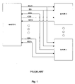
- FIG. 1 illustrates the basic prior-art SPI signaling protocol.
- the chip select signal ( CS) is used to address a particular slave device
- the master data output signal (SDI) is serial data transferred from the master to the slave on each serial clock
- the master data input signal (SDO) is serial data transferred from the slave to the master
- the serial clock (SCLK) provides the clocking for the transfer.
- the meaning of each bit or field of bits in transferred data is application defined, and can be commands, status, addresses, or data in a predefined sequence.
- the master device is typically a Digital Signal Processor (DSP), a microprocessor, or a microcontroller, and the slave device is often a single or multi-channel analog-to-digital converter (ADC) or ADC with on-board filtering.
- DSP Digital Signal Processor
- ADC analog-to-digital converter
- the most used operational mode for single channel or low data-rate multiple channel devices is synchronous control.
- the DSP selects a device, sends a command, and provides the clocks for the slave to execute the command and send the resulting data and status back to the processor.
- For asynchronous multiple channel devices allowing the devices to operate autonomously and then request output data transfers via an interrupt to the processor is a more efficient use of processing power.
- the high overhead associated with interrupt processing is costly, however, if there are a significant number of autonomous device channels having a high rate of data transfers. Therefore, an asynchronous control protocol that maximizes the data transferred while minimizing interrupts is preferred.
- FIG. 1 shows a common prior-art interface between a processor and multiple ADC channels.
- the processor starts multiple-channel data conversion by sending a signal, perhaps by sending an enable bit via the SDI pin with the appropriate channel selected by the CSn signal.
- the ADC acknowledges data ready (RDY) and, using an interrupt or polling routine, the processor recognizes data ready and controls the SPI bus to transfer the appropriate number of bits in the sample.
- RY data ready
- the processor must control each channel independently, and suffer the increased overhead for polling or interrupt handling.
- the processor must also handle each data sample independently.
- serial interface controller for transferring data between a data source having a least one channel and a processor.
- the serial interface controller has a plurality of control registers; the control registers in turn comprise a data structure for configuring the serial interface controller for a data transfer. That data structure further comprises a field for selectively setting the serial interface controller in its run mode or its configuration mode; a field for storing the I/O mode of the serial interface controller; a field for storing the address of the active data channel; and, a field for storing the system clock rate.
- control registers include fields for device identification, a flag for the run or configure mode, a I/O-mode control, a value for the channels active (in multi-channel implementations), the data source clock rate, the ADC clock rate, channel-status flags, the CIC decimation rate, the number of taps for FIR filters, and the filter coefficients corresponding to the number of FIR taps in a particular data source.
- An integrated circuit comprising a serial interface controller for transferring data between a data source and a processor is also disclosed.
- the serial interface controller in the integrated circuit has a plurality of control registers.
- the control registers have a data structure for configuring the serial interface controller for a data transfer.
- the data structure further comprises: a field for selectively setting the serial interface controller in its run mode or its configuration mode; a field for storing the I/O mode of the serial interface controller;
- a field for storing the address of the active data channel a field for storing the system clock rate.
- FIG. 1 depicts generally the prior-art serial-peripheral interface (SPI) signaling protocol.
- SPI serial-peripheral interface
- FIG. 2 is a block diagram showing the preferred embodiment.
- FIG. 3A-3C defines data and addressing formats for the preferred embodiment.
- FIG. 4A-4D illustrates the timing for the configuration mode data transfers of the preferred embodiment
- FIG. 5A-5C shows the timing for run mode transfers in the preferred embodiment.
- FIG. 2 presents a block diagram for an embodiment that has a multi-channel signal-processing capability ( 100 ) executing independently of a system processor, and a serial interface controller ( 200 ) that operates on a serial clock provided by the processor.
- the signal-processing capability ( 100 ) illustrated in FIG. 2 is an ADC and filtering function, although of course any application that requires the transfer of high rate, multiple channel data to a receiving processor could be conveniently adapted to the system and method here disclosed.
- the data source ( 100 ) thus need not be a digital-filter system.
- the serial interface communicates with the processor (not shown) through the standard Serial Peripheral Interface (SPI) I/O signals used by many processors to communicate with peripheral devices, where each device may be a single integrated circuit or a collection of circuits to perform desired processing functions.
- the processor may be a TI TMS 5500 series DSP, having an SPI port, its own memory space, and executing a stored program.
- FIG. 2 shows the signal lines relevant for this communication as follows:
- the example filter bank ( 100 ) may have one to n processing channels ( 110 ), and an output buffer ( 120 ) for each channel containing data to be transferred to the processor.
- the buffer ( 120 ) is preferably byte oriented; containing from one to m bytes of information, since most processor SPI controllers operate on bytes.
- the device is configured by serial transfers from the processor to the device control registers ( 220 ). These registers ( 220 ) activate and control all aspects of device operation. In the data conversion and filtering application shown, the registers contain all parameters to set the ADC conversion rate, define the filtering function, and therefore set the rate that results, or samples, are updated in the output buffers. In the embodiment depicted, these registers are shown in the following Table 1:
- CIC means a cascaded-integrator comb filter
- MSB means most-significant byte
- NSB means next-significant byte
- LSB means least-significant byte.
- 2 14 registers are provided, so many control channels beyond the seven shown in Table 1 are available for data sources having multiple channels.
- Addresses 0 through 4 are global device control bits. Address 0 is read-only and contains the device ID number. Address 1 contains a single bit that sets the device in the run mode. If this bit is off, the device is in the configure mode. Address 2 controls the I/O mode per the following definition:
- the System Clock Rate value at address 4 in the control register ( 220 ) is the clock rate of the data source ( 100 ). It may be asynchronous with the processor clock signal SCLK ( 330 ).
- the channel-status bits at address 6 in the control register ( 220 ) are determined by the nature of the data source ( 100 ). In the embodiment shown, the channel-status bits would be overflow or underflow bits for the output buffer ( 120 ) of each channel.
- control bits support a device with eight channels, each with an ADC, a CIC filter with a maximum decimation value of 65,536 (2 16 ), and an FIR filter with a maximum of 512 taps (256 coefficients or tap weights).
- the serial interface controller ( 200 ) circuitry contains an output shift register ( 210 ), and the multiplexers required to select, for parallel transfer to the register, any device channel's output buffer ( 120 ) or any byte of the device control registers ( 220 ).
- the output register is 24 bits wide to accommodate multi-channel data transfers, as shown in FIG. 3C .
- Multiplexer A in FIG. 2 ( 235 ) selects the device channel output buffer
- multiplexer B ( 260 ) selects the device control register ( 220 ) addressed by the address field (described below) of the input shift register ( 250 )
- multiplexer C ( 270 ) selects either the addressed device control register ( 220 ) or the selected device channel output buffer ( 120 ).
- the address decode and control function ( 230 ) decodes the address in the input shift register ( 250 ) and, based upon the current configuration or the read/write bit in that register, controls writing to the control registers ( 220 ).
- the register-select lines on multiplexer B ( 260 ) are generated by the address decode logic ( 230 ) to select the appropriate register to output on a read command.
- the channel-select lines on multiplexer A ( 235 ) are generated by the interface control logic ( 280 ) with inputs from the control registers ( 220 ). In run mode, the lines select the first (numerical order) channel output buffer with its channel-active bit set in the control register ( 220 ) at address 3 .
- the single channel bit is set in the control register ( 220 ) at address 2 , it will lock on the single active channel; if this bit is not set, the interface control logic will sequence through the active channels in response to a chip select ( 310 ) and SCLK sequence ( 330 ).
- the processor connected by way of the SPI bus controls all data transfers in and out of the filter bank ( 100 ) or similar device, according to its stored program.
- the data transferred and its interpretation is determined by the configuration mode of the device ( 100 ) and the prescribed protocol or format of each byte transferred.
- the serial interface controller ( 200 ) operates in two basic modes: the configuration mode, in which the processor is reading or writing data to the control registers ( 220 ), and the run mode, in which the processor is reading the data source ( 100 ) active-channel output buffers ( 120 ) and simultaneously writing to a subset of the control registers ( 220 ).
- the processor sets the device in the configure or run mode by setting a bit in a control register by a serial write to the device.
- FIG. 3 shows the data structures for these modes. Within these basic modes, the data formats can be further refined.
- the configure mode has an automatic address increment feature that permits a block of data to be read or written by shifting in a single address followed by a series of input bytes of write data via the SDI signal, or to output bytes of read data via the SDO signal as long as CS is held low and the processor continues to provide SCLK signals.
- the address auto-increment mode is set by a control write bit to a control register in the configure mode. When enabled, the interface controller interprets the first two serial bytes as a 14 bit address (as shown in FIG. 3A ).
- the controller then stores the next serial byte in the register addressed, if a write command, or reads and shifts out the register addressed if a read command; increments the address, and reads or writes the next byte, continuing the process until CS ( 310 ) is pulled high.
- the run mode has two data output formats: a single channel format that outputs two bytes of sample data from that channel with no control and status field ( FIG. 3B ), and a multi-channel format that outputs three bytes of data for each channel's sample, including an eight-bit control and status field and 16 bits of sample data ( FIG. 3C ).
- the number of bytes and the bit size of the control and data fields in the following discussion are, of course, only exemplary, and could differ in other implementations.
- the first 16 bits shifted into the input shift register ( 250 ) includes a read/write control bit and 14 bits of address. This address points to the control register ( 220 ) to be read or written.
- the last byte shifted in contains the data to be written for a write command, or the data from the register addressed to be shifted out for a read command.
- This read byte is transferred to the output shift register ( 210 ) and is clocked out to the processor. If the device is in the auto-increment mode, the read or write of data bytes continues without the processor transferring a new address, as long as CS ( 310 ) is held low.
- the run mode is set by the processor with a configure-mode data transfer.
- the run-mode format can be a two-byte data out field for a single channel configuration ( FIG. 3B ), or single or multiple three-byte fields for a multi-channel configuration ( FIG. 3C ).
- the processor can write data to the control registers ( 220 ) during a read of the output data, but to a restricted register set as explained below. This is required to take the device out of the run mode, for example, but may be used to set other registers within the current configuration. If the processor does not wish to modify a register, the serial input data must address an unused (or read only) register.
- the first byte shifted in is the write address and the second byte is the write data.
- the eight-bit address is a subset of the full 14-bit address space, thus allowing access to only the lower 256 (2 8 ) registers.
- the 16 bits of output samples are shifted out to the processor.
- the first 16 bits shifted in from the serial input as the processor reads the data output samples represents the address and write data, and the 24 bits shifted out to the processor represents 8 bits of status and control and 16 bits of sample data.
- the status and control byte includes a parity bit, a two-bit channel ID field, a new data flag to indicate that the output sample has been updated, and four channel-status bits.
- Other implementations for example a device with eight channels, can use the same general format by displaying fewer status bits and increasing the channel ID bit field to three bits. Only one status bit is absolutely required. In this case, it would tell the processor to read the status registers in the control registers to identify the change in device status.
- FIG. 4 shows the timing of signals in the configure mode.
- the processor starts a transfer by addressing the device with chip select ( 310 ) by bringing CS low from its normally high state, and using SCLK ( 330 ) to shift data into the input shift register ( 250 ) from the serial input signal SDI ( 340 ), or out of the output shift register ( 210 ) through the SDO line.
- the processor provides 24 SCLK's to transfer the address and first byte of data.
- the processor continues to provide clocks and data for as many sequentially addressed bytes of the control registers that it wishes to read or write.
- the interface control logic ( 280 ) addresses, with the first two bytes, the desired control register ( 220 ), and transfers this byte to the output shift register ( 210 ) to be shifted out the SDO pin ( 300 ) by the last eight SCLK's. If the first bit indicates write, the last eight bits are written to the addressed control register ( 220 ) by the address decode and write controller ( 230 ). If the device is in the auto-increment mode, bytes of information will continue to be input or output, with the controller ( 280 ) incrementing the internal address after each byte is written or transferred to the output shift register ( 210 ) and output SDO ( 300 ). The processor terminates the operation by removing chip select (bringing CS high).
- FIG. 5 shows signal timing for the run mode.
- the device sets and outputs the data ready RDY ( 320 ) signal when new data for the highest rate active channel is placed in that channel's output buffer ( 120 ), and, by default, selected to the output shift register ( 210 ).
- RDY is set when the fastest device channel, identified by a field in the control registers, transfers a new data sample to that channel's output buffer ( 120 ), setting a new data flag bit in the register at the same time.
- the new data flag, and thus the RDY signal are reset after the samples have been transferred to the output shift register ( 210 ).
- the processor which may poll RDY ( 320 ) or respond to the signal via an interrupt, addresses the device with chip select CS ( 310 ), and provides clock pulses through SCLK ( 330 ) to perform the transfers with write address and configuration data being input on the SDI ( 340 ) and sample data being output on the SDO ( 300 ). If the device is in a single-channel configuration, the processor provides 16 clocks to transfer the 16 bits of data from the active channel through the SDO signal ( 300 ), and, if desired, write a single byte into a control register ( 220 ). The processor completes the transfer by removing chip select ( 310 ). The write is performed to the address specified by the first eight bits of data in SDI ( 340 ) with the last eight bits being the data to be written.
- the processor reads 24 bits of data with 24 SCLK's from the first active channel; this being the default selection to the output shift register ( 210 ).
- the active channels are those that have been placed in the active mode by way of control fields in the control registers ( 220 ). Then the output shift register ( 210 ) is updated with the next active channel's output buffer ( 120 ) and this data is output with the next 24 SCLK's; this process continues until all active channel's output buffers ( 120 ) are transferred, and the processor terminates the transfer by removing chip select ( 310 ).
- the active channels are read out in numerical order. Note that a channel can be read that has not updated its output buffer ( 120 ) since the last read cycle.
- the processor recognizes this state by the new-data flag in the data format, and may choose not to store this data in processor memory. This flag is reset when that channel's output buffer ( 120 ) is transferred to the output shift register ( 210 ). After all active channels have been read; the processor terminates the transfer by removing chip select ( 310 ) and awaits the next RDY signal ( 320 ). In this mode the first 16 bits input on the SDI signal ( 340 ), shifted into the input shift register ( 250 ), are interpreted as eight bits of address and eight bits of data for writing to the restricted set of control registers ( 220 ). Again, the upper 6 bits of the 14 bit address are set to zero in the run mode. Thus only 256 registers are accessible.
- the processor will execute the transfer of sample data from all active channels. If there are multiple devices connected to the processor, the processor can read all active channels' sample outputs based on a single interrupt by addressing each device in numerical order with the individual device chip selects as shown in FIG. 1 . The processor has programmed all devices and thus knows which device has the highest rate channel. The only constraint is that the processor must transfer all channels samples before the highest sample rate device produces its next sample.
- the device can be set, by a control bit in the control registers, into a single channel interrupt mode.
- data ready RDY
- the processor will respond to data ready as before, but read only that channel that set data ready. This approach may be used if the sample rates for each channel are relatively slow and vary widely.
Landscapes
- Engineering & Computer Science (AREA)
- Theoretical Computer Science (AREA)
- Physics & Mathematics (AREA)
- General Engineering & Computer Science (AREA)
- General Physics & Mathematics (AREA)
- Information Transfer Systems (AREA)
Abstract
Description
| SDO | Serial Data Out (300) | ||
| |
Chip Select (active low) (310) | ||
| RDY | Ready (320) | ||
| SCLK | Serial Clock (330) | ||
| SDI | Serial Data In (340) | ||
| TABLE 1 | |
| Address | Data (8 bits) |
| 0 | Device ID (Read Only) |
| 1 | Run Mode |
| 2 | I/ |
| 3 | Channels |
| 4 | System Clock Rate (for data source operations) |
| 5 | ADC Clock Rate |
| 6 | Channel Status Bits |
| 7 | CIC Decimation MSB's |
| 8 | CIC Decimation LSB's |
| 9 | No. Taps MSB's |
| 10 | No. Taps LSB's |
| 11 | |
| 12 | |
| 13 | |
| 14 | |
| 15 | |
| 16 | |
| . . . | . . . |
| 776 | |
| 777 | |
| 778 | |
| 779-1552 | |
| 1553-2326 | |
| 2327-3100 | |
| 3101-3874 | |
| 3875-4648 | Channel 5 Control &Coefficients (Repeat of above) |
| 4647-5422 | Channel 6 Control &Coefficients (Repeat of above) |
| 5423-6196 | Channel 7 Control &Coefficients (Repeat of above) |
| Bits | Field Name | Definition |
| 0-2 | FastChannel | Fastest |
| 3 | not used | |
| 4 | EachChannelRDY | Set RDY for each channel; else fastest |
| channel | ||
| 5 | SingleChannel | Single-channel output if set; else multiple |
| channel | ||
| 6 | AutoIncrement | Auto-increment mode if set |
| 7 | not used | |
Claims (28)
Priority Applications (6)
| Application Number | Priority Date | Filing Date | Title |
|---|---|---|---|
| US11/223,356 US7533106B2 (en) | 2005-09-09 | 2005-09-09 | Data structures and circuit for multi-channel data transfers using a serial peripheral interface |
| EP06813824A EP1932075A4 (en) | 2005-09-09 | 2006-08-29 | Data structures and circuit for multi-channel data transfers using a serial peripheral interface |
| KR1020087008435A KR20080049099A (en) | 2005-09-09 | 2006-08-29 | Data structures and circuit for multi-channel data transfers using a serial peripheral interface |
| JP2008530083A JP2009514067A (en) | 2005-09-09 | 2006-08-29 | Data structure and circuit for multi-channel data transfer using serial peripheral interface |
| PCT/US2006/033469 WO2007032895A2 (en) | 2005-09-09 | 2006-08-29 | Data structures and circuit for multi-channel data transfers using a serial peripheral interface |
| CNA2006800327303A CN101331445A (en) | 2005-09-09 | 2006-08-29 | Data structures and circuit for multi-channel data transfers using a serial peripheral interface |
Applications Claiming Priority (1)
| Application Number | Priority Date | Filing Date | Title |
|---|---|---|---|
| US11/223,356 US7533106B2 (en) | 2005-09-09 | 2005-09-09 | Data structures and circuit for multi-channel data transfers using a serial peripheral interface |
Publications (2)
| Publication Number | Publication Date |
|---|---|
| US20070061342A1 US20070061342A1 (en) | 2007-03-15 |
| US7533106B2 true US7533106B2 (en) | 2009-05-12 |
Family
ID=37856531
Family Applications (1)
| Application Number | Title | Priority Date | Filing Date |
|---|---|---|---|
| US11/223,356 Expired - Fee Related US7533106B2 (en) | 2005-09-09 | 2005-09-09 | Data structures and circuit for multi-channel data transfers using a serial peripheral interface |
Country Status (6)
| Country | Link |
|---|---|
| US (1) | US7533106B2 (en) |
| EP (1) | EP1932075A4 (en) |
| JP (1) | JP2009514067A (en) |
| KR (1) | KR20080049099A (en) |
| CN (1) | CN101331445A (en) |
| WO (1) | WO2007032895A2 (en) |
Cited By (6)
| Publication number | Priority date | Publication date | Assignee | Title |
|---|---|---|---|---|
| US20110140533A1 (en) * | 2010-07-15 | 2011-06-16 | O2Micro, Inc. | Assigning addresses to multiple cascade battery modules in electric or electric hybrid vehicles |
| US8364873B2 (en) | 2010-03-09 | 2013-01-29 | Nuvoton Technology Corporation | Data transmission system and a programmable SPI controller |
| US20130120032A1 (en) * | 2011-11-11 | 2013-05-16 | Microchip Technology Incorporated | Analog Front End Device with Two-Wire Interface |
| US8688865B2 (en) * | 2012-03-30 | 2014-04-01 | Broadcom Corporation | Device identifier assignment |
| US10116288B2 (en) | 2017-02-07 | 2018-10-30 | Hamilton Sundstrand Corporation | Reduced overhead on digital signal processing for motor drive applications |
| US11256652B2 (en) * | 2019-06-20 | 2022-02-22 | Analog Devices International Unlimited Company | Multi-I/O serial peripheral interface for precision converters |
Families Citing this family (17)
| Publication number | Priority date | Publication date | Assignee | Title |
|---|---|---|---|---|
| US8095699B2 (en) * | 2006-09-29 | 2012-01-10 | Mediatek Inc. | Methods and apparatus for interfacing between a host processor and a coprocessor |
| US7613049B2 (en) * | 2007-01-08 | 2009-11-03 | Macronix International Co., Ltd | Method and system for a serial peripheral interface |
| US7823092B1 (en) | 2007-11-23 | 2010-10-26 | Altera Corporation | Method and apparatus for implementing a parameterizable filter block with an electronic design automation tool |
| CN101763300B (en) * | 2008-12-25 | 2012-03-07 | 佛山市顺德区顺达电脑厂有限公司 | Method for generating SATA (Serial Advanced Technology Attachment) port test signal |
| CN102255978B (en) * | 2010-05-20 | 2014-08-13 | 凹凸电子(武汉)有限公司 | Address configuration device, method and system |
| GB201102594D0 (en) * | 2011-02-15 | 2011-03-30 | Nordic Semiconductor Asa | Serial interface |
| US9176919B2 (en) * | 2012-06-06 | 2015-11-03 | Honeywell International Inc. | Process controller having multi-channel serial communications link |
| CN102819512B (en) * | 2012-06-28 | 2015-11-18 | 惠州市德赛西威汽车电子股份有限公司 | A kind of full-duplex communication device based on SPI and method thereof |
| US9152138B2 (en) | 2012-07-18 | 2015-10-06 | Honeywell International Inc. | Common collaboration context between a console operator and a field operator |
| GB2519350A (en) | 2013-10-18 | 2015-04-22 | St Microelectronics Grenoble 2 | Method and apparatus for supporting reprogramming or reconfiguring |
| CN103744806B (en) * | 2014-01-22 | 2017-01-18 | 张家港市复安电子科技有限公司 | Bit stream configuration method and bit stream configuration system |
| US9357551B2 (en) * | 2014-05-30 | 2016-05-31 | Corning Optical Communications Wireless Ltd | Systems and methods for simultaneous sampling of serial digital data streams from multiple analog-to-digital converters (ADCS), including in distributed antenna systems |
| GB2539445A (en) * | 2015-06-16 | 2016-12-21 | Nordic Semiconductor Asa | Data processing |
| KR102235290B1 (en) * | 2019-01-24 | 2021-04-02 | (주)실리콘인사이드 | Host and slave apparatus having cascade connection structure |
| US11392448B2 (en) * | 2020-10-20 | 2022-07-19 | Micron Technology, Inc. | Payload parity protection for a synchronous interface |
| EP4033370B1 (en) * | 2021-01-22 | 2023-11-15 | Aptiv Technologies Limited | Communications system and method of operating the same |
| CN113590520B (en) * | 2021-06-15 | 2024-05-03 | 珠海一微半导体股份有限公司 | Control method for automatically writing data in SPI system and SPI system |
Citations (17)
| Publication number | Priority date | Publication date | Assignee | Title |
|---|---|---|---|---|
| US4739324A (en) | 1986-05-22 | 1988-04-19 | Chrysler Motors Corporation | Method for serial peripheral interface (SPI) in a serial data bus |
| US4742349A (en) | 1986-05-22 | 1988-05-03 | Chrysler Motors Corporation | Method for buffered serial peripheral interface (SPI) in a serial data bus |
| US4816996A (en) | 1987-07-24 | 1989-03-28 | Motorola, Inc. | Queued serial peripheral interface for use in a data processing system |
| US4873623A (en) * | 1985-04-30 | 1989-10-10 | Prometrix Corporation | Process control interface with simultaneously displayed three level dynamic menu |
| US4958277A (en) | 1987-07-24 | 1990-09-18 | Motorola, Inc. | Queued serial peripheral interface for use in a data processing system |
| US5298921A (en) * | 1990-09-27 | 1994-03-29 | Advanced Micro Devices, Inc. | System for communicating with external device registers via two-byte data packets over a serial bus |
| US5630152A (en) | 1992-05-18 | 1997-05-13 | Motorola, Inc. | Communication protocol between master and slave device with register information sharing |
| US5828592A (en) | 1997-03-12 | 1998-10-27 | Information Storage Devices, Inc. | Analog signal recording and playback integrated circuit and message management system |
| US5954813A (en) | 1994-11-10 | 1999-09-21 | Motorola, Inc. | Data processor with transparent operation during a background mode and method therefor |
| US6167466A (en) * | 1997-07-09 | 2000-12-26 | Texas Instruments Incorporated | Multi-channel serial port with programmable features |
| US6302654B1 (en) | 2000-02-29 | 2001-10-16 | Copeland Corporation | Compressor with control and protection system |
| US6366768B1 (en) | 1998-11-09 | 2002-04-02 | Motorola, Inc. | Circuit and method of frequency synthesizer control with a serial peripheral interface |
| US6664833B1 (en) | 2000-11-20 | 2003-12-16 | Intersil Americas, Inc. | Dual-edge function clock generator and method of deriving clocking signals for executing reduced instruction sequences in a re-programmable I/O interface |
| US6665593B2 (en) | 2001-03-09 | 2003-12-16 | Robert Bosch Gmbh | Device for data transmission between vehicle sensors and a processor in a controller |
| US6687769B2 (en) | 2001-03-16 | 2004-02-03 | Texas Instruments Incorporated | Serial peripheral interface with high performance buffering scheme |
| US6691183B1 (en) | 1998-05-20 | 2004-02-10 | Invensys Systems, Inc. | Second transfer logic causing a first transfer logic to check a data ready bit prior to each of multibit transfer of a continous transfer operation |
| US6871292B1 (en) | 2000-11-20 | 2005-03-22 | Intersil Americas, Inc. | Sequencer and method of selectively inhibiting clock signals to execute reduced instruction sequences in a re-programmable I/O interface |
Family Cites Families (10)
| Publication number | Priority date | Publication date | Assignee | Title |
|---|---|---|---|---|
| JPH0455721A (en) * | 1990-06-25 | 1992-02-24 | Nippon Denshi Kagaku Kk | Thermocouple temperature recorder |
| JPH07160515A (en) * | 1993-12-07 | 1995-06-23 | Mitsumi Electric Co Ltd | Interrupt signal generator |
| JPH0877133A (en) * | 1994-09-06 | 1996-03-22 | Mitsubishi Denki Semiconductor Software Kk | A/d conversion device |
| JPH08272765A (en) * | 1995-03-30 | 1996-10-18 | Hitachi Ltd | Semiconductor integrated circuit and motor driving control circuit |
| JP3206483B2 (en) * | 1997-03-17 | 2001-09-10 | 日本電気株式会社 | Interrupt control device |
| JPH11136128A (en) * | 1997-10-30 | 1999-05-21 | Nec Eng Ltd | Ad converter |
| US6456219B1 (en) * | 2000-02-22 | 2002-09-24 | Texas Instruments Incorporated | Analog-to-digital converter including two-wire interface circuit |
| JP2002182930A (en) * | 2000-12-18 | 2002-06-28 | Hitachi Kokusai Electric Inc | Interruption controller |
| JP2002261609A (en) * | 2001-03-01 | 2002-09-13 | Toshiba Corp | Analog/digital converter and its signal processing method |
| US6831583B1 (en) * | 2002-11-05 | 2004-12-14 | Analog Devices, Inc. | Integrated circuit comprising a microprocessor and an analogue to digital converter which is selectively operable under the control of the microprocessor and independently of the microprocessor, and a method for operating the integrated circuit |
-
2005
- 2005-09-09 US US11/223,356 patent/US7533106B2/en not_active Expired - Fee Related
-
2006
- 2006-08-29 JP JP2008530083A patent/JP2009514067A/en active Pending
- 2006-08-29 CN CNA2006800327303A patent/CN101331445A/en active Pending
- 2006-08-29 KR KR1020087008435A patent/KR20080049099A/en not_active Application Discontinuation
- 2006-08-29 EP EP06813824A patent/EP1932075A4/en not_active Withdrawn
- 2006-08-29 WO PCT/US2006/033469 patent/WO2007032895A2/en active Search and Examination
Patent Citations (17)
| Publication number | Priority date | Publication date | Assignee | Title |
|---|---|---|---|---|
| US4873623A (en) * | 1985-04-30 | 1989-10-10 | Prometrix Corporation | Process control interface with simultaneously displayed three level dynamic menu |
| US4739324A (en) | 1986-05-22 | 1988-04-19 | Chrysler Motors Corporation | Method for serial peripheral interface (SPI) in a serial data bus |
| US4742349A (en) | 1986-05-22 | 1988-05-03 | Chrysler Motors Corporation | Method for buffered serial peripheral interface (SPI) in a serial data bus |
| US4816996A (en) | 1987-07-24 | 1989-03-28 | Motorola, Inc. | Queued serial peripheral interface for use in a data processing system |
| US4958277A (en) | 1987-07-24 | 1990-09-18 | Motorola, Inc. | Queued serial peripheral interface for use in a data processing system |
| US5298921A (en) * | 1990-09-27 | 1994-03-29 | Advanced Micro Devices, Inc. | System for communicating with external device registers via two-byte data packets over a serial bus |
| US5630152A (en) | 1992-05-18 | 1997-05-13 | Motorola, Inc. | Communication protocol between master and slave device with register information sharing |
| US5954813A (en) | 1994-11-10 | 1999-09-21 | Motorola, Inc. | Data processor with transparent operation during a background mode and method therefor |
| US5828592A (en) | 1997-03-12 | 1998-10-27 | Information Storage Devices, Inc. | Analog signal recording and playback integrated circuit and message management system |
| US6167466A (en) * | 1997-07-09 | 2000-12-26 | Texas Instruments Incorporated | Multi-channel serial port with programmable features |
| US6691183B1 (en) | 1998-05-20 | 2004-02-10 | Invensys Systems, Inc. | Second transfer logic causing a first transfer logic to check a data ready bit prior to each of multibit transfer of a continous transfer operation |
| US6366768B1 (en) | 1998-11-09 | 2002-04-02 | Motorola, Inc. | Circuit and method of frequency synthesizer control with a serial peripheral interface |
| US6302654B1 (en) | 2000-02-29 | 2001-10-16 | Copeland Corporation | Compressor with control and protection system |
| US6664833B1 (en) | 2000-11-20 | 2003-12-16 | Intersil Americas, Inc. | Dual-edge function clock generator and method of deriving clocking signals for executing reduced instruction sequences in a re-programmable I/O interface |
| US6871292B1 (en) | 2000-11-20 | 2005-03-22 | Intersil Americas, Inc. | Sequencer and method of selectively inhibiting clock signals to execute reduced instruction sequences in a re-programmable I/O interface |
| US6665593B2 (en) | 2001-03-09 | 2003-12-16 | Robert Bosch Gmbh | Device for data transmission between vehicle sensors and a processor in a controller |
| US6687769B2 (en) | 2001-03-16 | 2004-02-03 | Texas Instruments Incorporated | Serial peripheral interface with high performance buffering scheme |
Non-Patent Citations (3)
| Title |
|---|
| Freescale Semiconductor, Inc., SPI Block Guide V04.01, Jan. 21, 2000, Revised Jul. 14, 2004, Motorola, Inc., Document No. S12SPIV4/D. |
| International Preliminary Examining Authority, International Application No. PCT/US06/33469, International Preliminary Report on Patentability, Oct. 21, 2008. |
| International Searching Authority, International Application No. PCT/US06/33469, International Search Report and the Written Opinion, Mar. 26, 2008. |
Cited By (8)
| Publication number | Priority date | Publication date | Assignee | Title |
|---|---|---|---|---|
| US8364873B2 (en) | 2010-03-09 | 2013-01-29 | Nuvoton Technology Corporation | Data transmission system and a programmable SPI controller |
| US20110140533A1 (en) * | 2010-07-15 | 2011-06-16 | O2Micro, Inc. | Assigning addresses to multiple cascade battery modules in electric or electric hybrid vehicles |
| US8525477B2 (en) | 2010-07-15 | 2013-09-03 | O2Micro, Inc. | Assigning addresses to multiple cascade battery modules in electric or electric hybrid vehicles |
| US20130120032A1 (en) * | 2011-11-11 | 2013-05-16 | Microchip Technology Incorporated | Analog Front End Device with Two-Wire Interface |
| US8742968B2 (en) * | 2011-11-11 | 2014-06-03 | Microchip Technology Incorporated | Analog front end device with two-wire interface |
| US8688865B2 (en) * | 2012-03-30 | 2014-04-01 | Broadcom Corporation | Device identifier assignment |
| US10116288B2 (en) | 2017-02-07 | 2018-10-30 | Hamilton Sundstrand Corporation | Reduced overhead on digital signal processing for motor drive applications |
| US11256652B2 (en) * | 2019-06-20 | 2022-02-22 | Analog Devices International Unlimited Company | Multi-I/O serial peripheral interface for precision converters |
Also Published As
| Publication number | Publication date |
|---|---|
| WO2007032895A2 (en) | 2007-03-22 |
| WO2007032895A3 (en) | 2008-06-19 |
| JP2009514067A (en) | 2009-04-02 |
| EP1932075A4 (en) | 2009-09-09 |
| KR20080049099A (en) | 2008-06-03 |
| EP1932075A2 (en) | 2008-06-18 |
| CN101331445A (en) | 2008-12-24 |
| US20070061342A1 (en) | 2007-03-15 |
Similar Documents
| Publication | Publication Date | Title |
|---|---|---|
| US7533106B2 (en) | Data structures and circuit for multi-channel data transfers using a serial peripheral interface | |
| US8914551B2 (en) | Sensor polling unit for microprocessor integration | |
| EP2097828B1 (en) | Dmac to handle transfers of unknown lengths | |
| JP2001142842A (en) | Dma handshake protocol | |
| US20020184453A1 (en) | Data bus system including posted reads and writes | |
| US6539448B1 (en) | Priority first come first serve interrupt controller | |
| JP2010033614A (en) | Input/output processor | |
| JPH08235850A (en) | Depth-/width-adjustable fifo buffer for variable-width data transfer | |
| JPH05298060A (en) | Format conversion circuit | |
| US6728797B2 (en) | DMA controller | |
| EP0464848B1 (en) | Structure for enabling direct memory-to-memory transfer | |
| KR102235290B1 (en) | Host and slave apparatus having cascade connection structure | |
| US20060184708A1 (en) | Host controller device and method | |
| EP2089804B1 (en) | Peripheral supplied addressing in a simple dma | |
| US6883041B2 (en) | Direct memory access device | |
| CN100541469C (en) | Host access interface and its implementation | |
| JP3773574B2 (en) | Apparatus and method for inserting an address into a data stream in a data processing system | |
| WO1987003114A1 (en) | Method and apparatus for interfacing between analog signals and a system bus | |
| US7420486B1 (en) | Control of analog to digital conversion for analog I/O boards | |
| US11029914B2 (en) | Multi-core audio processor with phase coherency | |
| CN100353296C (en) | Method of controlling out put data to bus in peripheral equipment and its related device | |
| JPH0778780B2 (en) | Bus width controller | |
| JP4097377B2 (en) | Microcomputer | |
| JP3127620B2 (en) | Command decoding device | |
| JPH05342090A (en) | Data processor |
Legal Events
| Date | Code | Title | Description |
|---|---|---|---|
| AS | Assignment |
Owner name: QUICKFILTER TECHNOLOGIES, INC., TEXAS Free format text: ASSIGNMENT OF ASSIGNORS INTEREST;ASSIGNORS:MAGDEBURGER, THOMAS;HEADLEY, AARON;REEL/FRAME:017222/0265 Effective date: 20051025 |
|
| AS | Assignment |
Owner name: SORRENTO INVESTMENT GROUP, LLC, PENNSYLVANIA Free format text: SECURITY AGREEMENT;ASSIGNOR:QUICKFILTER TECHNOLOGIES, INC.;REEL/FRAME:018635/0022 Effective date: 20061211 Owner name: ARGONAUT 10 LLC, MASSACHUSETTS Free format text: SECURITY AGREEMENT;ASSIGNOR:QUICKFILTER TECHNOLOGIES, INC.;REEL/FRAME:018635/0022 Effective date: 20061211 |
|
| AS | Assignment |
Owner name: QUICKFILTER TECHNOLOGIES, INC., TEXAS Free format text: RELEASE BY SECURED PARTY;ASSIGNORS:ARGONAUT 10 LLC;SORRENTO INVESTMENT GROUP, LLC;REEL/FRAME:020403/0473 Effective date: 20071217 |
|
| AS | Assignment |
Owner name: SPINNAKER CAPITAL LLC SECURITY HOLDING AS NOMINEE Free format text: SECURITY AGREEMENT;ASSIGNOR:QUICKFILTER TECHNOLOGIES, INC.;REEL/FRAME:021867/0900 Effective date: 20081117 Owner name: STAIANO, EDWARD, TEXAS Free format text: SECURITY AGREEMENT;ASSIGNOR:QUICKFILTER TECHNOLOGIES, INC.;REEL/FRAME:021867/0900 Effective date: 20081117 |
|
| AS | Assignment |
Owner name: QUICKFILTER TECHNOLOGIES, LLC, TEXAS Free format text: ASSIGNMENT OF ASSIGNORS INTEREST;ASSIGNOR:QUICKFILTER TECHNOLOGIES INC.;REEL/FRAME:022494/0917 Effective date: 20090404 |
|
| STCF | Information on status: patent grant |
Free format text: PATENTED CASE |
|
| AS | Assignment |
Owner name: STAIANO, EDWARD, TEXAS Free format text: SECURITY AGREEMENT;ASSIGNOR:QUICKFILTER TECHNOLOGIES LLC;REEL/FRAME:022618/0158 Effective date: 20090404 Owner name: SPINNAKER CAPITAL LLC SECURITY HOLDING AS NOMINEE Free format text: SECURITY AGREEMENT;ASSIGNOR:QUICKFILTER TECHNOLOGIES LLC;REEL/FRAME:022618/0158 Effective date: 20090404 |
|
| REMI | Maintenance fee reminder mailed | ||
| AS | Assignment |
Owner name: QUICKFILTER TECHNOLOGIES, TEXAS Free format text: RELEASE BY SECURED PARTY;ASSIGNOR:ARGONAUT 10 LLC;REEL/FRAME:029850/0992 Effective date: 20130221 |
|
| FPAY | Fee payment |
Year of fee payment: 4 |
|
| SULP | Surcharge for late payment | ||
| AS | Assignment |
Owner name: MILLER, FRED, TEXAS Free format text: ASSIGNMENT OF ASSIGNORS INTEREST;ASSIGNOR:GLAST, PHILLIPS & MURRAY, P.C.;REEL/FRAME:032146/0530 Effective date: 20140205 Owner name: THOMAS, JOHN A., TEXAS Free format text: ASSIGNMENT OF ASSIGNORS INTEREST;ASSIGNOR:GLAST, PHILLIPS & MURRAY, P.C.;REEL/FRAME:032146/0530 Effective date: 20140205 Owner name: GLAST, PHILLIPS & MURRAY, P.C., TEXAS Free format text: ASSIGNMENT OF ASSIGNORS INTEREST;ASSIGNOR:QUICKFILTER TECHNOLOGIES, LLC;REEL/FRAME:032145/0278 Effective date: 20140129 |
|
| AS | Assignment |
Owner name: GOOGLE INC., CALIFORNIA Free format text: ASSIGNMENT OF ASSIGNORS INTEREST;ASSIGNORS:THOMAS, JOHN A.;MILLER, FRED;REEL/FRAME:037309/0698 Effective date: 20150723 |
|
| FPAY | Fee payment |
Year of fee payment: 8 |
|
| AS | Assignment |
Owner name: GOOGLE LLC, CALIFORNIA Free format text: CHANGE OF NAME;ASSIGNOR:GOOGLE INC.;REEL/FRAME:044101/0610 Effective date: 20170929 |
|
| FEPP | Fee payment procedure |
Free format text: MAINTENANCE FEE REMINDER MAILED (ORIGINAL EVENT CODE: REM.); ENTITY STATUS OF PATENT OWNER: SMALL ENTITY |
|
| LAPS | Lapse for failure to pay maintenance fees |
Free format text: PATENT EXPIRED FOR FAILURE TO PAY MAINTENANCE FEES (ORIGINAL EVENT CODE: EXP.); ENTITY STATUS OF PATENT OWNER: SMALL ENTITY |
|
| STCH | Information on status: patent discontinuation |
Free format text: PATENT EXPIRED DUE TO NONPAYMENT OF MAINTENANCE FEES UNDER 37 CFR 1.362 |
|
| FP | Lapsed due to failure to pay maintenance fee |
Effective date: 20210512 |