US7398259B2 - Training of a physical neural network - Google Patents
Training of a physical neural network Download PDFInfo
- Publication number
- US7398259B2 US7398259B2 US10/969,789 US96978904A US7398259B2 US 7398259 B2 US7398259 B2 US 7398259B2 US 96978904 A US96978904 A US 96978904A US 7398259 B2 US7398259 B2 US 7398259B2
- Authority
- US
- United States
- Prior art keywords
- neural network
- nanoconductors
- synaptic
- rule
- electromechanical
- Prior art date
- Legal status (The legal status is an assumption and is not a legal conclusion. Google has not performed a legal analysis and makes no representation as to the accuracy of the status listed.)
- Expired - Lifetime, expires
Links
Images


Classifications
-
- G—PHYSICS
- G06—COMPUTING; CALCULATING OR COUNTING
- G06N—COMPUTING ARRANGEMENTS BASED ON SPECIFIC COMPUTATIONAL MODELS
- G06N3/00—Computing arrangements based on biological models
- G06N3/02—Neural networks
- G06N3/08—Learning methods
-
- Y—GENERAL TAGGING OF NEW TECHNOLOGICAL DEVELOPMENTS; GENERAL TAGGING OF CROSS-SECTIONAL TECHNOLOGIES SPANNING OVER SEVERAL SECTIONS OF THE IPC; TECHNICAL SUBJECTS COVERED BY FORMER USPC CROSS-REFERENCE ART COLLECTIONS [XRACs] AND DIGESTS
- Y10—TECHNICAL SUBJECTS COVERED BY FORMER USPC
- Y10S—TECHNICAL SUBJECTS COVERED BY FORMER USPC CROSS-REFERENCE ART COLLECTIONS [XRACs] AND DIGESTS
- Y10S977/00—Nanotechnology
- Y10S977/70—Nanostructure
- Y10S977/701—Integrated with dissimilar structures on a common substrate
- Y10S977/712—Integrated with dissimilar structures on a common substrate formed from plural layers of nanosized material, e.g. stacked structures
-
- Y—GENERAL TAGGING OF NEW TECHNOLOGICAL DEVELOPMENTS; GENERAL TAGGING OF CROSS-SECTIONAL TECHNOLOGIES SPANNING OVER SEVERAL SECTIONS OF THE IPC; TECHNICAL SUBJECTS COVERED BY FORMER USPC CROSS-REFERENCE ART COLLECTIONS [XRACs] AND DIGESTS
- Y10—TECHNICAL SUBJECTS COVERED BY FORMER USPC
- Y10S—TECHNICAL SUBJECTS COVERED BY FORMER USPC CROSS-REFERENCE ART COLLECTIONS [XRACs] AND DIGESTS
- Y10S977/00—Nanotechnology
- Y10S977/70—Nanostructure
- Y10S977/701—Integrated with dissimilar structures on a common substrate
- Y10S977/72—On an electrically conducting, semi-conducting, or semi-insulating substrate
-
- Y—GENERAL TAGGING OF NEW TECHNOLOGICAL DEVELOPMENTS; GENERAL TAGGING OF CROSS-SECTIONAL TECHNOLOGIES SPANNING OVER SEVERAL SECTIONS OF THE IPC; TECHNICAL SUBJECTS COVERED BY FORMER USPC CROSS-REFERENCE ART COLLECTIONS [XRACs] AND DIGESTS
- Y10—TECHNICAL SUBJECTS COVERED BY FORMER USPC
- Y10S—TECHNICAL SUBJECTS COVERED BY FORMER USPC CROSS-REFERENCE ART COLLECTIONS [XRACs] AND DIGESTS
- Y10S977/00—Nanotechnology
- Y10S977/70—Nanostructure
- Y10S977/724—Devices having flexible or movable element
-
- Y—GENERAL TAGGING OF NEW TECHNOLOGICAL DEVELOPMENTS; GENERAL TAGGING OF CROSS-SECTIONAL TECHNOLOGIES SPANNING OVER SEVERAL SECTIONS OF THE IPC; TECHNICAL SUBJECTS COVERED BY FORMER USPC CROSS-REFERENCE ART COLLECTIONS [XRACs] AND DIGESTS
- Y10—TECHNICAL SUBJECTS COVERED BY FORMER USPC
- Y10S—TECHNICAL SUBJECTS COVERED BY FORMER USPC CROSS-REFERENCE ART COLLECTIONS [XRACs] AND DIGESTS
- Y10S977/00—Nanotechnology
- Y10S977/70—Nanostructure
- Y10S977/734—Fullerenes, i.e. graphene-based structures, such as nanohorns, nanococoons, nanoscrolls or fullerene-like structures, e.g. WS2 or MoS2 chalcogenide nanotubes, planar C3N4, etc.
- Y10S977/742—Carbon nanotubes, CNTs
Definitions
- Embodiments generally relate to molecular technology, such as, for example, nanotechnology. Embodiments also relate to neural networks and neural computing systems and teaching methods thereof. Embodiments are additionally related to plasticity rules and training rules, such as, for example Anti-Hebbian and Hebbian rules.
- Neural networks are computational systems that permit computers to essentially function in a manner analogous to that of the human brain. Neural networks do not utilize the traditional digital model of manipulating 0's and 1's. Instead, neural networks create connections between processing elements, which are equivalent to neurons of a human brain. Neural networks are thus based on various electronic circuits that are modeled on human nerve cells (i.e., neurons).
- a neural network is an information-processing network, which is inspired by the manner in which a human brain performs a particular task or function of interest.
- Computational or artificial neural networks are thus inspired by biological neural systems.
- the elementary building blocks of biological neural systems are the neuron, the modifiable connections between the neurons, and the topology of the network.
- Biologically inspired artificial neural networks have opened up new possibilities to apply computation to areas that were previously thought to be the exclusive domain of human intelligence. Neural networks learn and remember in ways that resemble human processes. Areas that show the greatest promise for neural networks, such as pattern classification tasks, speech and image recognition are areas where conventional computers and data-processing systems have had the greatest difficulty.
- artificial neural networks are systems composed of many nonlinear computational elements operating in parallel and arranged in patterns reminiscent of biological neural nets.
- the computational elements, or nodes, are connected via variable weights that are typically adapted during use to improve performance.
- neural net models can explore many competing hypothesis simultaneously using massively parallel nets composed of many computational elements connected by links with variable weights.
- neuron-like nodes can output a signal based on the sum of their inputs, the output being the result of an activation function.
- a neural network there exists a plurality of connections, which are electrically coupled among a plurality of neurons. The connections serve as communication bridges among of a plurality of neurons coupled thereto.
- a network of such neuron-like nodes has the ability to process information in a variety of useful ways. By adjusting the connection values between neurons in a network, one can match certain inputs with desired outputs.
- Neural networks are currently used in applications such as noise filtering, face and voice recognition and pattern recognition. Neural networks can thus be utilized as an advanced technique for processing information.
- Neural networks that have been developed to date are largely software-based.
- a true neural network e.g., the human brain
- a true neural network e.g., the human brain
- half of a human brain can suffer a lesion early in its development and not seriously affect its performance.
- Software simulations are slow because during the learning phase a standard computer must serially calculate connection strengths. When the networks get larger (and therefore more powerful and useful), the computational time becomes enormous.
- networks with 10,000 connections can easily overwhelm a computer.
- the human brain has about 100 billion neurons, each of which can be connected to about 5,000 other neurons.
- a network is trained to perform a specific task, perhaps taking many days or months to train, the final useful result can be built or “downloaded” onto a piece of hardware and also mass-produced. Because most problems requiring complex pattern recognition are highly specific, networks are task-specific. Thus, users usually provide their own, task-specific training data.
- the fastest software simulations available can perform up to approximately 18 million interconnects per second.
- Such speeds however, currently require expensive super computers to achieve.
- Even so, approximately 18 million interconnects per second is still too slow to perform many classes of pattern classification tasks in real time. These include radar target classifications, sonar target classification, automatic speaker identification, automatic speech recognition, electrocardiogram analysis, etc.
- neural network systems has lagged somewhat behind their theoretical potential due to the difficulties in building neural network hardware. This is primarily because of the large numbers of neurons and weighted connections required. The emulation of even of the simplest biological nervous systems would require neurons and connections numbering in the millions and/or billions.
- neural network hardware systems Due to the difficulties in constructing such highly interconnected processors, currently available neural network hardware systems have not approached this level of complexity. Another disadvantage of hardware systems is that they typically are often custom designed and configured to implement one particular neural network architecture and are not easily, if at all, reconfigurable in implementing different architectures. A true physical neural network chip, with the learning abilities and connectivity of a biological network, has not yet been designed and successfully implemented.
- Nanotechnology generally refers to nanometer-scale manufacturing processes, materials and devices, as associated with, for example, nanometer-scale lithography and nanometer-scale information storage. Nanometer-scale components find utility in a wide variety of fields, particularly in the fabrication of micro-electrical and micro-electromechanical systems (commonly referred to as “MEMS”). Micro-electrical nano-sized components include transistors, resistors, capacitors and other nano-integrated circuit components. MEMS devices include, for example, micro-sensors, micro-actuators, micro-instruments, micro-optics, and the like.
- CMOS complementary metal oxide semiconductor
- Nanoconductors are tiny conductive tubes (i.e., hollow) or wires (i.e., solid) with a very small size scale (e.g., 0.7 to 300 nanometers in diameter and up to 1 mm in length). Their structure and fabrication have been widely reported and are well known in the art. Carbon nanotubes, for example, exhibit a unique atomic arrangement, and possess useful physical properties such as one-dimensional electrical behavior, quantum conductance, and ballistic electron transport.
- Carbon nanotubes are among the smallest dimensioned nanotube materials with a generally high aspect ratio and small diameter.
- High-quality single-walled carbon nanotubes can be grown as randomly oriented, needle-like or spaghetti-like tangled tubules. They can be grown by a number of fabrication methods, including chemical vapor deposition (CVD), laser ablation or electric arc growth.
- CVD chemical vapor deposition
- laser ablation or electric arc growth.
- Carbon nanotubes can be grown on a substrate by catalytic decomposition of hydrocarbon containing precursors such as ethylene, methane, or benzene. Nucleation layers, such as thin coatings of Ni, Co, or Fe are often intentionally added onto the substrate surface in order to nucleate a multiplicity of isolated nanotubes. Carbon nanotubes can also be nucleated and grown on a substrate without a metal nucleating layer by using a precursor including one or more of these metal atoms. Semiconductor nanowires can be grown on substrates by similar processes.
- a molecular wire crossbar memory device can be constructed from crossbar arrays of nanowires sandwiching molecules that act as on/off switches.
- Such a device can be formed from a plurality of nanometer-scale devices, each device comprising a junction formed by a pair of crossed wires where a single wire crosses another and at least one connector species connects the pair of crossed wires in the junction.
- the connector species comprises a bi-stable molecular switch.
- the junction forms either a resistor or a diode or an asymmetric non-linear resistor.
- the junction has a state that is capable of being altered by application of a first voltage and sensed by the application of a second, non-destructive voltage.
- a series of related patents attempts to cover everything from molecular logic to how to chemically assemble these devices.
- Such a molecular crossbar device has two general applications.
- the notion of transistors built from nanotubes and relying on nanotube properties is being pursued.
- two wires can be selectively brought to a certain voltage and the resulting electrostatic force attracts them. When they touch, the Van der Walls force keeps them in contact with each other and a “bit” is stored.
- the connections in this apparatus can therefore be utilized for a standard (i.e., binary and serial) computer.
- the inventors of such a device thus desire to coax a nanoconductor into a binary storage media or a transistor. As it turns out, such a device is easier to utilize as a storage device.
- a semiconductor integrated circuit i.e., a computer chip.
- Such a device which can be referred to as a “physical neural network chip” or a “synapse chip” is thus disclosed herein.
- Such a device if successfully implemented would be well suited for use with neural networks.
- a physical neural network including an adaptive neural network, which can be formed and implemented utilizing nanotechnology.
- nanoconductors such as, for example, nanowires and/or nanotubes.
- AHAH Anti-Hebbian and Hebbian
- a physical neural network can be configured utilizing molecular technology, wherein the physical neural network comprises a plurality of molecular conductors, which form neural network connections thereof.
- a training mechanism can be provided for training the physical neural network to accomplish a particular neural network task based on a neural network training rule.
- the neural network connections are formed between pre-synaptic and post-synaptic components of the physical neural network.
- the neural network dynamic and modifiable connections for adaptive signal processing.
- the neural network training mechanism can be based, for example, on the Anti-Hebbian and Hebbian (AHAH) rule and/or other plasticity rules.
- AHAH Anti-Hebbian and Hebbian
- the molecular conductors can be disposed within a solution and can be configured, for example, as nanoparticles suspended in the solution.
- a mechanism can also be provided for dynamically implementing variable connections from the neural network connections.
- Such a mechanism can be implemented as a dielectrophoretic assembly of nanoparticles in the solution.
- the nanoparticles suspended in the solution are subject to a dielectrophoretic force and exposed to time-varying electric fields, wherein the dielectrophoretic force is utilized to attract or repel the nanoparticles to an electrode gap formed between at least one pre-synaptic electrode and at least one post-synaptic electrode of the physical neural network.
- the nanoparticles suspended in the solution can comprise semi-conducting nanoparticles, and or other nanoparticles such as, for example, carbon nanotubes and/or carbon nanowires.
- FIG. 1 illustrates a graph of two-dimensional data space, where features can be recognized as clusters of data points in accordance with an embodiment of the present invention
- FIG. 2 illustrates a data space graph illustrating a plasticity rule, wherein an initial random weight vector splits a feature in two, so that the decision boundary is moved to cleanly divide features from one another in accordance with an embodiment of the present invention
- FIG. 3 illustrates a group of data space graphs that together illustrate the application of the Anti-Hebbian and Hebbian (AHAH) rule in accordance with an embodiment of the present invention
- FIG. 4 illustrates data space graphs demonstrating the result of lateral inhibition, where the same initial weight vectors are forced into separate states in accordance with an embodiment of the present invention
- FIG. 5 illustrates a graph of a data space, wherein the polarity of four of five neurons is flipped and the average output from all neurons can be analyzed so that an ensemble can be made selective to Feature (2) thereof in accordance with an embodiment of the present invention
- FIG. 6 illustrates a graph illustrating how a row of neural ensembles can be utilized to extract a sub-phonemic base set, which in turn can be utilized to extract a phonemic base set, in accordance with an embodiment of the present invention
- FIG. 7 illustrates a group of graphs demonstrating how one neuron can be moved from a state that divides particular features from one another, in accordance with an embodiment of the present invention
- FIG. 8 illustrates a graph depicting the average output of a neuron in response to Feature 2depicted in FIG. 7 , in accordance with an embodiment of the present invention
- FIG. 9 illustrates a graph illustrating a mean ensemble output to specific and pulse-modulated inhibition and teacher signal applied data, in accordance with an embodiment of the present invention.
- FIG. 10 illustrates a high level block diagram depicting the interaction between a physical neural network implementation, a mathematical implementation and a mathematical description in accordance with an embodiment of the present invention
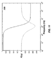
- FIG. 11 illustrates a graph of angular frequency versus frequency in Hertz, which can be adapted to illustrate an embodiment of the present invention
- FIG. 12 illustrates a graph of capacitance versus time, which can be adapted to illustrate an embodiment of the present invention
- FIG. 13 illustrates a graph depicting data illustrating two-quadrant control over a KnowmTM connection, in accordance with an embodiment of the present invention
- FIG. 14 illustrates a schematic diagram of a two-quadrant multiplication circuit configuration for a neural implementation, which can be implemented in accordance with an embodiment of the present invention
- FIG. 15 illustrates a schematic diagram of a KnowmTM network, which can be implemented in accordance with an embodiment of the present invention
- FIG. 16 illustrates a high-level pictorial diagram depicting chip stacking with vertical KnowmTM connections, in accordance with one embodiment of the present invention
- FIG. 17 illustrates a high-level block diagram depicting a system, which can be implemented in accordance with a preferred embodiment of the present invention.
- FIG. 18 illustrates a high-level block diagram depicting a system, which can be implemented in accordance with an alternative embodiment of the present invention.
- the physical neural network disclosed herein with respect to one or more embodiments can be referred to generically as a KnowmTM.
- the terms “physical neural network” and “Knowm” can thus be utilized interchangeably to refer to the same device, network, or structure.
- the term “Knowm” can also refer to a semiconductor implementation, such as a physical neural network chip and/or synapse chip. Note that the terms “physical neural network chip” and “synapse chip” can also be utilized herein to refer generally to the same or analogous type of KnowmTM device.
- a physical neural network (i.e., a KnowmTM enabled physical neural network) generally should possess two basic components to function properly.
- a physical neural network should have one or more neuron-like nodes that sum a signal and output a signal based on the amount of input signal received.
- Such a neuron-like node is generally non-linear in output. In other words, there should be a certain threshold for input signals, below which nothing can be output and above which a constant or nearly constant output is generated or allowed to pass. This is considered the basic building block of all neural networks, and can be accomplished by an activation function.
- the second requirement of a physical neural network is the inclusion of a connection network composed of a plurality of interconnected electrodes (i.e., nanoconnections).
- Intelligent Signal Processing attempts to address the problems that current technology has been unable to solve. If a problem can be distilled into a clear and sequential mathematical algorithm, the problem can be solved utilizing current computing platforms. Many problems have been solved in this manner; however, these strategies fail as attempts are made to solve distinctly human problems, such as visual recognition. Such human problems require massive amounts of processing “noisy” data. Visual object recognition represents one example where a designer would desire to build a system capable of finding and tracking objects.
- KnowmTM technology thus bridges these fields by offering three distinct advantages.
- an algorithm capable of extracting object information in association with a KnowmTM connection network e.g., physical neural network
- the building blocks for assembling variable pieces into a coherent whole can be utilized to solve problems such as visual object recognition.
- radio identification modules can be attached to all current speed limit signs. An on-board receiver can then keep track of the speed limit. Simple enough. What about avoiding other cars? Again, a solution can be envisioned where each car contains a GPS system and a radio transceiver. The position of the car can be broadcast to all other cars, which use this information to control the car. This is still a feasible route to take. But what about the occasional deer that wonders into the road at night, frozen in the headlights? Or even worse, what about a child crossing the street, running after a soccer ball kicked into the road? What about recognizing the road itself? One can see where this line of thought is headed.
- the information can be contained in the system itself.
- An example is a mechanism for repairing DNA in living cells.
- the algorithm discussed herein is based on the notion that the inherent structure of the environment, the “data stream” itself, contains the information for both learning and self-repair through coupling with a plasticity rule.
- Information about the environment may be strengthened and retained by constant exposure to one's environment, and more specifically the memory of an event may be retained without subsequent exposure to the event.
- the system is a dynamic network of continuously active plastic synapses. The result is a self-building and self-repairing computational system capable of object extraction.
- the object of the neural-processing game is to find features (objects) within the data and to reliably act on those features.
- the circuitry of the cerebellum attempts to learn a sequence of events, such as for example, the complicated motion and coordination of muscles required to ride a bicycle.
- a specific input can be referred to as a “feature” in the environment.
- the feature can represent many possibilities, from complicated generalization to an extremely specific event.
- the input Before an action can be performed in response to a particular input, the input must have a distinct representation by either the firing of a neuron or the firing of a specific group of neurons.
- the chip must map the input space (pixels, speech waveform, etc) to a specific sequence of standardized digital outputs. These output need to be standardized so that traditional computer system may reliably act on the information.
- FIG. 1 illustrates a graph 100 of two-dimensional data space.
- FIG. 1 illustrates a graph 100 of two-dimensional data space.
- this two-dimensional space out of all possible points, only a small subset ever occurs, which can be recognized as Features 1 through 5 as depicted in graph 502 of FIG. 1 .
- This smaller subset can be referred to as the “structure” of the environment.
- Our goal is to find a neural network capable of distinguishing one feature from every other feature.
- a mechanism is required for active repair.
- the network should maintain that function in the face of changes to the network, such as neural death or random changes to synaptic values.
- the mechanism for network adaptation must be continuously active.
- a plasticity rule is therefore sought that allows learning, while actively adapting the synaptic weights so as to retain that learned state.
- Another problem that one faces is that a particular environmental input may not occur; yet a mechanism is required, which is capable of maintaining specificity to this input. In other words, the retention of a neural response is required in the absence of rehearsal (i.e. remembering how to ride a bicycle after 20 years on not riding). Because neurons die, the plasticity rule must not maintain a specific weight vector, but rather a specific neural state.
- the activation, Y, of the neuron can be provided as indicated in equation (1) below:
- the simple neural model described herein is capable of dividing its synaptic space into two parts, i.e. it can fire or not fire in response to an input.
- FIG. 1 it is immediately clear that no single neuron is capable of becoming selective to any arbitrary feature. Whereas features 1, 3 and 4 are linearly separable, features 2 and 5 are not. Because any one neuron may only make a “slice”, one appropriate question is, “what is the best slice?”
- One type of slice can be eliminated, which is a slice that occurs at the boundary of the data distribution. Such a situation does not provide information and is therefore not wanted. Is there an efficient way to “dice up” the space, keeping in mind that in the end a specific response to only one feature is desired? With a mind on efficiency, another type of slice can be eliminated, or at the very least minimized. Ideally, the slice should cleanly divide the data space into two half's without dividing any one feature. In the field of machine learning, this can be seen as “maximizing the support vectors”.
- FIG. 2 illustrates a data space graph 200 illustrating a plasticity rule, wherein an initial random weight vector splits a feature in two, so that the decision boundary is moved to cleanly divide features from one another in accordance with an embodiment of the present invention.
- the rule must depend on pre- and post-synaptic activity.
- the post-synaptic activity is proportional to the perpendicular distance from the decision boundary. The farther “over the line” the input, the higher the post-synaptic activity becomes. If one thinks of the plasticity rule as a mechanism that moves the decision boundary by a small amount in response to an input, then the final decision boundary in FIG. 2 represent a balance, where the activation (or non-activation) from Feature (1) is balanced by the activation of the other features.
- the variable ⁇ w i represents the change in the i th weight, while the variable ⁇ represents a learning rate.
- the variable x i represents the i th pre-synaptic activity and y is the post synaptic activity.
- This learning rule is a generalized Hebbian learning rule where (1 ⁇ y 2 ) controls the transition from Hebbian to Anti-Hebbian learning. Equation (2) can be referred to as the Anti-Hebbian and Hebbian rule, AHAH, (pronounced aha!).
- AHAH Anti-Hebbian and Hebbian rule
- Such a learning rule can converge to multiple local minima and depends on the initial conditions, learning rate a and noise level of the input data. Some of these local minima are useful for classification purposes while others are not.
- This rule has been found to extract the Independent Components (IC) of data and is consequently very useful for classification tasks. Such a rule was used to determine the final decision boundary in graph 200 of FIG. 2 and indeed can accomplish the desired goals outlined earlier
- FIG. 3 illustrates a group of data space graphs 302 , 304 , 306 , 308 that together illustrate the application of the Anti-Hebbian and Hebbian (AHAH) rule in accordance with an embodiment of the present invention.
- AHAH Anti-Hebbian and Hebbian
- the rule quickly converges to the data structure illustrated in graph 304 .
- graph 306 converges to graph 308 .
- random initial weights certainly do not guarantee the weight vectors find a unique slice after convergence with AHAH.
- two weight vectors fell into the same (or opposite) fix points between Features (1) and (2).
- neural circuit In terms of integration of a lateral inhibition function into a chip structure, it should be recognized that our final “neural circuit” will represent a bank of neurons, not an individual neuron.
- the non-synaptic functions of neural summation and lateral inhibition (no plasticity on inhibitory connections) will be accomplished with traditional CMOS technology, whereas the synapses and their plastic nature are emulated with self-organizing nanoparticles.
- the scaling rule must be overshadowed by the plasticity rule that determines the fixed points, otherwise the weights will converge to a global minimum (the minor component) and all states will be lost.
- the scaling rule must be highly non-linear.
- ⁇ is large, typically greater than 4. Because the desired effect of an activity-dependant scaling rule is to prevent “run away weights”, a limit on the magnitude of a weight would also have the desired effect.
- weight restriction represents one possible solution, as the conductance of a physical connection should not fall below zero or above a certain maximum.
- Graph 502 of FIG. 5 therefore illustrates the result of an activity-dependant rule applied to the initial weight configuration of graph 404 depicted in FIG. 4 . Notice how the outlying decision boundary is brought back into the distribution, yet the fixed-points remain undisturbed.
- the fundamental “unit” of computation in this case, can be the neural ensemble that responds selectively to one feature.
- Each ensemble is cable of mutual inhibition so as to converge to separate states.
- An ever-present and highly nonlinear activity-dependant-scaling rule maintains decision boundaries in the distribution, while a training signal (to be discussed shortly) can be utilized to prevent “forbidden” states from being occupied.
- a total of five neural ensembles would be needed to isolate each feature, while each ensemble would require anywhere from one neuron (linearly separable, i.e. feature 1,3 and 4) to three or more (non-linearly separable, i.e. feature 2 and 5).
- a non-linearly separable feature may be isolated by an ensemble by forcing only certain states to be occupied.
- the neurons are held stable by the underlying structure of the distribution, i.e., the fixed points of the plasticity rule.
- a neuron's stability is related to the features themselves. Suppose, for instance, that Feature (1) suddenly disappeared, or that its occurrence was suddenly highly unlikely. In effect, this would send the corresponding neuron, whose decision boundary happens to distinguish the feature, off into the fringes of the distribution. The scaling rule (if there is one) would pull the decision boundary back into the remaining distribution, and the state would be lost along with the ability to distinguish the feature. What is needed is a “base set” of features that occur regularly. Such a base set was illustrated in the previous figures.
- Higher-level features can be distinguished from the base set.
- speech where an individual word may not be spoken for many days or years, but the underlying phonemes occur quite regularly.
- the neural ensemble can be thought of as a unit for recognition of a word, and the individual states of neurons within the ensemble occupying a state made stable by the frequent occurrence of the underlying phonemes.
- selective response to a phoneme is the result of a neural ensemble in which each neuron has found a stable sub-phonemic structure.
- a row of neural ensembles would be used to extract a sub-phonemic base set, which in turn is used to extract the phonemic base set.
- Such a circumstance is illustrated in graph 602 of FIG. 6 .
- Another example is vision.
- the stable states occur at a small scale, and are sometimes recognized as edge filters. From a stable basis set, higher-level feature detectors can be constructed.
- the feature detectors themselves simply represent a cluster of neurons occupying distinct states that happen to all agree when it comes to the presence of one feature. It is interesting to note that just this sort of organization is present in the human cortex: cortical columns in lower level visual cortex become selective to edges of varying degrees of orientation, and this structure is determined early in life, during a “critical period”.
- learning represents the selective occupation of fixed points of a plasticity rule operating on a continually present environmental structure.
- the normal plasticity rule should be disturbed.
- the weight update is zero. If we desire to train a network to learn a particular feature, we can proceed as follows. An input is presented. If the input happens to be from the target feature, we activate each neuron in the cluster by a set amount, say 1.1. Looking at the figure, if the neural output (y) was +1, the addition of 1.1 would result in no weight modification, as the squash sum of total activation would still be +1 (tanh(1+1.1) ⁇ 1). If the neural output were ⁇ 1, however, the addition of 1.1 would result in significant Hebbian learning and push the state closer to zero activation, which will in turn cause more of a weight update.
- FIG. 8 illustrates a graph 800 depicting the average output of a neuron in response to Feature 2 depicted in FIG. 7 , in accordance with an embodiment of the present invention.
- Graph 800 therefore illustrates the average output of the neuron in response to Feature 2 illustrated in 702 , 704 , 706 of FIG. 7 .
- Pre-Learning the feature is clearly in a state that classifies feature 2 as ( ⁇ 1).
- arrow 806 represents the teaching signal.
- Arrow 808 represents post-learning activities.
- Pre-learning activities are therefore separated from the teaching signal by line 810 in graph 800 .
- An inset graph 802 depicted in FIG. 8 illustrates that as the decision boundary penetrates the feature; the rate of convergence goes from exponential (approaching feature) to linear (in the feature).
- the linear regime is due to the much smaller variance of the plasticity rule. For instance, when the decision boundary splits the features in two, roughly the same amount of inputs fall on either side of the boundary. As the positive inputs do not contribute to weight modification, the rate of convergence is roughly equal to the integration of all inputs resulting in activation from ⁇ 1 to 0. If the activation function is steep, one can expect there to be a roughly equal force pulling the decision boundary through the feature. That is, until the decision boundary reaches the other side of the feature, in which case there are no more inputs immediately to the negative portion of the boundary and the convergence rate quickly goes to zero.
- a neural cluster capable of selective activation to a feature within the environment can now be constructed. Such a situation can be demonstrated in two-dimensions, but a case can be made for the validity of real-world data of large dimension. At this point, it is worth reviewing the general concept, and how it relates to higher dimensions. Given any data set, be it visual, auditory, or something else entirely, the underlying assumption is that there is some inherent structure at some scale, and this structure occurs frequently.
- FIG. 9 illustrates a graph 900 of the average ensemble output from a group of twenty neurons in response to each feature in the distribution depicted and described earlier with respect to FIGS. 1-5 , in accordance with an embodiment of the present invention.
- Features 1 and 3 are represented by line 908
- Feature 4 is represented by line 906
- Feature 5 is represented by line 904
- Feature 2 represented by line 902 .
- Pulsed Inhibition as indicated by arrow 910 in graph 900 of FIG. 9 can be utilized to separate the states. Recall that a neuron can only achieve the minimal energy state if the teaching signal was turned off.
- a pulsed-teaching signal can be utilized.
- Application of a teacher signal is indicated in FIG. 9 by arrow 912 .
- the neurons can only completely converge in the absence of a teaching or inhibitory signal.
- the teaching (or inhibitory) signal “kicks” the neuron beyond the local energy maxima so that it can descend into other minima.
- Graph 900 of FIG. 9 illustrates that the mean output of +1 indicates that every neuron in the ensemble occupies a state that puts Feature 2 “on the positive side of the fence”. Notice how the ensemble state went through intermediate, and stable, states before converging to total agreement. This is due to the pulsed teaching signal. Also note the considerably selective response to Feature 2 when compared to the other Features. The same procedure can be utilized, for example, to construct neural ensembles capable of extracting base sets from speech waveforms.
- a continuously active plasticity rule can be utilized to create an energy landscape where learning is a function of selective occupation of fixed-point states. What remains to be seen is a by-product of the dynamic nature of this process: adaptive fault tolerance.
- neural networks exhibit inherent fault tolerance due to connection multiplicity and a distributed representation, the continuous adaptation of weights can provide substantial improvements.
- the AHAH plasticity rule can greatly improve fault tolerance for random weight fluctuations and input-line faults by maintaining weight equilibrium in a local attractor state.
- connection strengths change continuously, but input lines are also lost to neural death. Stability under this type of dynamic environment seems to require a dynamic network capable of tracking and dealing with the faults and changes in neural circuitry as they occur and thus requires a mechanism for the constant modification of weights.
- the neural network community has proposed several architectures like Hopfield Networks and Self Organizing Maps that are inherently parallel and exploit system dynamics to solve computational problems. Solutions are represented as equilibrium points and the convergence of the system effectively provides self-organized fault tolerance. This type of approach appears ideal for fault tolerant computing with next generation devices, but to date has been limited to specific applications for which these systems have been proposed (e.g. associative memories and clustering).
- a plasticity rule should correct for these fluctuations and maintain the weight vector about the initial values. For an unsupervised rule, this requires that the weight vector used for classification also be a fixed point of the plasticity rule. Because it is desirable to use the same plasticity rule for different classification tasks, it is necessary for the rule to have many fixed points associated with many different possible classifications. The goal is to find an online mechanism for updating the weights to help account for the faults.
- J(y) stochastic gradient ascent of an objective function J(y)
- Equation (8) E ⁇ x ⁇ is the expectation with respect to x.
- the quadratic objective function of equation (8) possesses a global maximum (or minimum) and the learning rule converges to a single fixed point.
- the weight vector will converge to the principle component of the data regardless of the initial, or desired value of w.
- Higher-order objective functions might be utilized in accordance with alternative embodiments of the present invention.
- Such objective functions generally possess multiple local maxima and learning rules that converge to one of many fixed points.
- the multiple fixed points of higher-order learning rules can provide a novel mechanism for learning and fault tolerance in dynamic neural networks.
- the basic assumption is that an objective function can be found that is related to, at some level, the desired behavior for a neuron. If this is the case, it follows that there is a local maximum, and hence a learning rule with a fixed point close to (or at) the desired value of w when there are no faults. Thus, the performance of the output neuron will not degrade significantly with a continuously active learning rule and no faults present. Additionally, with faults present, the input statistics can shift the local fixed point and the learning rule can track this shift by modifying w accordingly.
- Such a constraint also means that the sensitivity to second order statistics can be reduced and preprocessing steps such as, for example, whitening (de-correlating the data) is not required.
- Inputs consisted of D vectors are presented repetitively, where D is the number of inputs to the neuron (not including redundancy). Every vector is a normal distribution with magnitude one, centered at the respective input line and of variance ⁇ . Thus, with very small variance the inputs become non-overlapping and orthogonal.
- synapse faults are random fluctuations of synapse values and are computed by adding a random number generated from a normal distribution with magnitude N amp to each weight on every time step.
- Random Input faults are computed by replacing the appropriate value of a percentage of all input lines with a random value on every time step. The random value can be selected from a uniform distribution between ⁇ 1 and 1.
- Dead input faults can be computed by replacing the appropriate value of a percentage of all input lines with zero.
- the network can be run until the first error is detected and the time step of the first error recorded, the first error being defined as the first disagreement between the faulted network and an equivalent network with no faults and no adaptation.
- FIG. 1 herein illustrates the mean time-to-first-error as a function of the redundancy of the connections.
- the performance of AHAH can be compared to a network with no weight adaptation under identical faults.
- the stability of the connections grows exponentially with increased redundancy and only linearly, as expected, for no adaptation. This can be explained in the following way. Every weight in the network is either positive or negative. If inputs are orthogonal, the weights define the class: positive weights for the (+) class and negative weights for the ( ⁇ ) class. Suppose a weight is faulted. With no redundancy, or a redundancy of two, there is no information available as to what sign the weight should be.
- Input faults can occur in a few flavors. First, the input simply goes to zero, a.k.a ‘dead input fault’. Second, the input may still carry a signal, but has been corrupted by noise and is no longer correlated with the desire classification, a.k.a a ‘random input fault’.
- the faults can also occur in two ways: all at once or accumulate gradually over time. Both random and dead input faults can be investigated under sudden and gradual fault introductions. For a gradual fault introduction, a specified percentage of total input lines are made faulty in a linear schedule from time-step (ts) 1000 to 9000.
- FIG. 3 illustrates the mean error as a function of variance of input for a 50% gradual random fault introduction.
- AHAH performs substantially better than no adaptation, and only slightly worse for small variances.
- the optimal variance is a result of the chosen ⁇ .
- FIGS. 5-6 include data repeats the experiments FIGS. 3-4 for dead input faults.
- AHAH performs better than no adaptation.
- One particularly interesting observation is the sharp transition from 50% error to no error.
- the connection network described herein can adapt to sudden input faults. As one can appreciate, there is little difference between the performance of AHAH and the control for sudden dead input faults. This is contrasted with the performance of gradual fault introductions. The full power of the adaptation rule can be appreciated when applied to the context of gradual fault introductions, which are presumably more likely in any physical implementation of a neural system.
- the on-line adaptation of weights is a powerful mechanism for network robustness in the face of faults and has application not only in explaining the ability of biological neural networks to stabilize memories in the face of changing network conditions, but also in the construction of nano-scale device architectures.
- plasticity rules can provide a similar, if not a better degree of fault tolerance.
- the ability of a network to adapt to faults is a direct result of the attractor state of the network.
- a plasticity rule can be found that contains a fixed point at a desired weight vector, the rule will display a degree of fault tolerance.
- rules like AHAH is that the same rule can provide for both powerful statistical analysis such as finding IC's useful for classification, and using the IC's to provide linearly separable outputs necessary for high degrees of fault tolerance in down-stream layers.
- dielectrophoresis (DEP) with respect to the physical neural network of the present invention.
- DEP dielectrophoresis
- pre- and post-synaptic electrodes form electrode gaps.
- the electric field generated by pre- and post-synaptic neural circuitry precipitates particles from solution and they aggregate at the gap.
- the gradient and frequency dependence allows for control over connection formation and thus a mechanism for modifiable connects in a hybrid “wet” neural chip.
- connection properties can be tailored to a desired behavior.
- Contaminants are generally not as conductive, or vary in their permittivity, from the desired nanoparticles.
- ac-induced DEP can attract only the desired nanoparticles and leave contaminates behind. This creates cleaner connections.
- an alternate form of a Knowm connection requires only semi-conducting nanoparticles.
- the DEP force has successfully been used to separate metallic from semi-conducting nanotubes, and can thus be used as a mechanism to sort nanoparticles on-chip to attain only the semi-conducting particles.
- FIG. 10 illustrates a high level block diagram depicting the interaction between a physical neural network implementation as indicated at block 1006 , a mathematical implementation as depicted by block 1002 and a mathematical description as depicted at block 1004 in accordance with an embodiment of the present invention.
- a neural network gets its power from many individual neurons all working together at the same time.
- a computer can accomplish only one, or a few tasks, simultaneously.
- a computer is exactly the wrong architecture for emulating a neural network.
- the phenomenal success and speed of modern computers has created the impression that with the current trend of performance increase, a personal computer will eventually be capable of running arbitrarily complex programs. What is not generally realized is that if the “arbitrarily complex program” is a neural network, the personal computer will have to rely on entirely different architectures. If the goal is to fit a neural network capable of biological performance into a small stand-alone chip that consumes little power, the solution is to forget about anything serial.
- a physical neural network is simply a neural network in which the mathematical operations necessary to emulate the network, including the plastic nature of a synapse, are entirely accomplished by physical processes. In other words, synaptic attenuation, neural summation, activation, and synaptic modification are all physical properties of the network.
- a KnowmTM network is a physical network. Traditional analog neural networks use the tools currently available to emulate the function of a synapse, i.e. (transistors, capacitors, etc).
- Plasticity is simply the ability to modify a connection strength. By what rules the connection is modified, be it supervised or unsupervised, is secondary to the fundamentally important requirement that the connection possesses in some way the ability to both strengthen and weaken. If a connection can be electrically modified in a relatively predictable way, and the connection is very small, then it is likely that it will find use in some sort of neural structure. After a potential connection is found, however, it is helpful to ask oneself exactly what types of algorithms the connection will be used for. In neural algorithms the connection dynamics are usually fairly slow and the connection values have at least 4-bit precision.
- a KnowmTM network is a potential solution to building biological-scale neural networks as well as vastly miniaturizing current networks.
- the size of biological-scale networks precludes any “hard-coding” of synaptic strengths because even the most powerful computers cannot determine what the synaptic strengths should be.
- Synaptic modification is a dynamic process anyway, so hard-coding is very much out of the question. Without the ability for connections to obey a plasticity rule, with every connection adapting in parallel, large functional networks cannot be built. Indeed, the functionality they inherit lies in the way synaptic strengths are modified.
- a plasticity rule that is non-local will not practically work for large networks. Ideally, the only information a synapse should use to modify its strength is the pre- and post-synaptic neural activations. In other words, the plasticity rule needs to be unsupervised. Although a Knowm Synapse can be “coaxed” into behaving like a supervised connection, the basic idea is that any artificial synapse (and any biological synapse for that matter) only has two terminals.
- the transistor Take for example the basic building block of all modern electronics: the transistor.
- a transistor is basically a valve. By controlling the base voltage, one can control the current flow through the source and drain. This is certainly a modifiable connection.
- the problem is providing the correct base voltage, at the correct time, to emulate the desired plasticity rule.
- One will have to design an additional circuit, which takes as its input the pre-and post-synaptic terminals and provide as its output the base voltage needed keep the transistor conductance at the appropriate level (as determined by the plasticity rule).
- KnowmTM represents a solution in a solution, and it is the liquid suspension that makes possible the properties we desire. Besides the dynamics of connection modification, there are some other important properties a KnowmTM connection must have.
- a synapse is the junction between a pre-synaptic terminal (the axon) and a post-synaptic terminal (the dendrite). Because of the chemical nature, the connection is one-way. Signals can only travel from axon to dendrite. Electrically, a network of neurons must be connected by a “matrix” of electrodes. Without a one-way connection, this matrix no longer represents a structure that reliably routes the pre-synaptic signals to the appropriate post-synaptic electrode, but a very large “percolation” resistive network. Such feature can be utilized in structures such as an “artificial retina”, but it is hardly appropriate for directing neural signals.
- connection it is thus necessary for the connection to behave like a diode and only conduct in one direction.
- a number of methodologies can be implemented for accomplishing such a diode functionality. For example, by properly doping the nanoparticles and the pre- and post-synaptic electrodes one can imagine a diode-like connection. It is believed that the dielectrophoretic assembly of certain types of nanoparticles can create a one-way connection. Although the mechanism is not yet fully understood, the result is indeed a one-way connection from dielectrophoretically-aligned particles between two electrodes (of the same material). This diode-like behavior is definitely surprising, but the results are certainly there and the property is vital for a successful neural network.
- a KnowmTM connection must be much smaller, less conductive and composed of many wires (for greater resistance variation).
- the dielectrophoretic force is dependant on the field gradient, often expressed in volts per meter. As the dimensions decrease, a smaller voltage is required to produce the same field gradient. Although a larger field gradient is required to overcome Brownian motion, theoretical work indicates that sub-10 nm particles can be trapped within a 10 nm electrode gap with less that 1 Volt.
- the resistances of a KnowmTM connection would most likely be measured in giga-ohms, depending on the nanoparticles. With this resistance, the power dissipation per connection would be in the pico-watt range.
- Hebbian learning amounts to principal component analysis of the input data.
- the principle components are useful for classification, one is generally interested in high-order features. For example, imagine that a network is being presented with images, and a layer of neurons with receptive fields in the image space. In other words, each neuron receives input from a subset of all image pixels.
- Hebbian learning determines which “pixels” are most active, but may not explain which combinations of pixels are correlated with each other.
- a pre-whitening of the data can be performed to eliminate first-order statistics. If this is done, the picture will still be recognizable. If one performs a pre-whitening to eliminate phase information, the picture will look like static! So it is understandable that the representations an unsupervised (higher-order) learning rule converges to is a set of features that are useful for classifications. In other words, an unsupervised rule can be found that does exactly (or very close to) what a supervised rule will do, i.e. perform a higher-order statistical analysis of the data.
- the synapse is a connection formed by the aggregation of particles floating around in a liquid. By application of appropriate voltage signals, the connection can be strengthened and weakened. But the basic picture is one of a dynamical system. Particles are being pushed and pulled in many directions and it is the group behavior that determines the over-all connection properties. So one does not actually “update” a connection value. It is perhaps more accurate to speak of “pushing” and “pulling” the connection in different directions. Unsupervised learning can be seen in the same light, as it the rule “pushes” and “pulls” the connection values until they reach stable points characterized by some statistic of the input data.
- an unsupervised learning rule is unavoidable.
- the dynamic nature of the connection will require, to some extent, an ever-present restoring force keeping the synaptic values from dissolving.
- the problem is that one usually wants to teach the network how to perform (i.e. associate the correct labels with the data). But a supervised and an unsupervised rule can be made to match.
- Recent work indicates that it is possible to teach a network in a supervised way and keep the network stable with an unsupervised rule.
- the dynamics of the connection provide a high degree of “stable adaptation” capable of reconfiguring connections to track non-stationary data. This is a bit ironic because particles in solution bring to mind the notion of instability.
- the reality is that such a connection can be more stable and powerful than other physical implementation because the fixed point (i.e. energy minimum) of the system is a weight vector that solves the problem.
- a nano-scale neural architecture should possess nano-connections, but neural implementations must be large enough to allow for larger fan-in and fan-outs. It is often unnoticed that when it comes to neural systems, the problem is simply connecting the neurons. If the fundamental device is a single-electron transistor, one is faced with two problems. First, algorithms need to be designed to match the physical restrictions of the device. Second, when one has a novel molecular device, how does one actually assemble all the pieces?
- KnowmTM is very unique in that it simultaneously solves these problems.
- the device physics embody a type of iterative learning common to many neural algorithms.
- the force responsible for connection modification also allows self-assembly.
- Knowm technology it should be possible to create a chip that emulates well-understood algorithms, offers a tremendous performance increase over current technology, holds promise for future algorithms based on alternate feedback mechanisms-and most importantly-assembles itself.
- the problem is abstracted to a solution space that limits the networks growth. For example, by sharing the same wires, the neurons will eventually interfere with each other when they fire at the same time. As coherent oscillations have been found in many biological networks, and oscillations have been used successfully in image segmentation, a structure that cannot cope with coherent oscillations would be a poor solution. Alternately, a mechanism can be built that prevents neurons from using the same wire at the same time. But again, this forces a bottleneck in the system. In the end, the best way to build a neural network is to connect all the neurons with dedicated wires. The tools of modern VLSI have limited this, but a KnowmTM connection can make it possible. Of course, it is not only a matter of making a connection. The connection must be extraordinarily small and is preferably unidirectional should also obey a plasticity rule.
- X and Y may be thought of as a voltage, current, frequency or perhaps even a phase in an electrical signal.
- a vital feature of Hebbian learning is its multiplicative nature, or more specifically, the necessity that the physical quantities that represent X or Y be able to take on negative values. Mathematically, this can result from either a negative input “X”, or a negative output “Y”. Physically, this is a difficult task. If one can find a physical connection that can be strengthened and weakened by pre- or post-synaptic activity, then this connection can be used to emulate most plasticity rules (subject to the temporal nature of connection modification). A feedback mechanism, presumably within the neural circuit, can provide the necessary signal for connection modification.
- ⁇ * ⁇ - j ⁇ ⁇ with ⁇ the conductivity, ⁇ the permittivity and ⁇ the angular frequency of the applied electric field.
- the particle in some instances, is more conductive than the suspension, so this restricts us to positive dielectrophoresis for lower frequencies and negative dielectrophoresis for higher frequencies.
- graph 1100 of FIG. 11 where the real part of the CM factor is generally drawn as a solid line.
- connection can exhibit a frequency and gradient dependence
- Resistance modification represents one potential area for explaining how the conductance of a connection can change.
- the change in conductance of a connection is linearly proportional to the dielectrophoretic force as indicated by equation (16):
- FIG. 12 illustrates a graph 1200 of capacitance versus time, which can be adapted to illustrate an embodiment of the present invention.
- FIG. 12 illustrates a graph 1200 of capacitance versus time, which can be adapted to illustrate an embodiment of the present invention.
- this corresponds to, for example, a routing circuit that directs two different signals. If Y is positive, then a low frequency signal is routed to the post-synaptic electrode to induce positive dielectrophoresis. This will strengthen the connection and allow for positive multiplication. On the other hand, if Y is negative then the routing circuit will direct a high frequency signal to induce negative dielectrophoresis and weaken the connection (negative multiplication). Whereas H(Y) controls the sign of the update, a DC bias controls the magnitude of the update. Such a circumstance is illustrated in graph 1300 of FIG. 13 .
- FIG. 13 illustrates a graph 1300 depicting data illustrating two-quadrant control over a KnowmTM connection, in accordance with an embodiment of the present invention.
- the pre-synaptic voltage, V pre controls the pre-synaptic contribution to connection formation
- the post-synaptic DC bias, V post controls the post-synaptic magnitude to the weight update
- the post-synaptic frequency, H(Y) controls the sign of the post-synaptic weight update.
- two-quadrant multiplication is achieved by routing two externally generated signals and saving the cost of a current-to-frequency function for each neural circuit.
- the general connection update takes the form, where f(V pre , V post ) represent a non-linear transformation of the input signals into a post-synaptic bias and frequency voltage signal.
- Two-quadrant multiplication as depicted in FIG. 13 is sufficient for any neural implementations provided inhibitory inputs are treated separately.
- a general diagram of such a circuit is depicted in FIG. 14 , where excitatory and inhibitory inputs are treated separately.
- FIG. 14 illustrates a schematic diagram of a two-quadrant multiplication circuit 1400 , which can be utilized for a neural implementation, in accordance with an embodiment of the present invention.
- Circuit 1400 generally includes a positive input electrode 1412 and a negative input electrode 1414 .
- An electrode gap is located between positive input electrode 1412 and an electrode portion 1406 .
- an electrode gap is located between negative input electrode 1414 and an electrode portion 1408 .
- a plurality of nanoparticles 1402 can be suspended in a solution between the electrode gap located between positive input electrode 1412 and electrode portion 1406 .
- a plurality of nanoparticles 1404 can be suspended in a similar or identical solution in the electrode gap located between negative input electrode 1414 and electrode portion 1408 .
- Nanoparticles 1402 and 1404 can be exposed to time-varying electric fields and can also experience a dielectrophoretic force. Such a force can be used to attract and repel nanoparticles in the respective electrode gaps. The electrical resistance across the gap is dependent on the relative number of nanoparticles bridging the gap (e.g., more particles, less resistance and visa versa). At a basic level, this particle bridge can be thought of as a synapse.
- Circuit 1400 additionally includes an output electrode 1416 , which produces data generated from neural network support circuitry 1414 .
- circuit 1400 can be easily constructed utilizing a few transistors. Arbitrary plasticity rules can be implemented by suitable characterization of nanoparticles 1402 and 1404 and relatively simple transistor circuits (amplifiers, routers, etc) can be provided by neural network support circuitry 1414 . Although circuit 1400 is relatively compact, the dielectrophoretic force allows for further simplifications, while retaining and even gaining functionality. Circuit 1400 can be implemented in the context of a KnowmTM network.
- the dielectrophoretic force can be dependant on both the conductance and permittivity of the nanoparticle and medium.
- the conductance is negligible and the dielectrophoretic force is dominated by the effective moment of the dielectric particle.
- the relative permittivity of the particle, ⁇ p , and the medium, ⁇ m controls the sign of the Clausius-Mossotti function.
- the Clausius-Mossotti factor is dominated by the conductivity of the particle and medium, ⁇ p and ⁇ m , if the timescale of the changing electric field is smaller than the relaxation time constant associated with the accumulation of free charge at the surface of the particle. This is known as the Maxwell-Wagner relaxation time constant:
- ⁇ MW ⁇ p + 2 ⁇ ⁇ m ⁇ p + 2 ⁇ ⁇ m ( 21 )
- semi-conducting particles where a “gate” voltage can control the conductivity of the particle.
- Such semi-conducting particles can be implemented, for example, as nanoparticles 1402 and 1404 depicted in FIG. 14 .
- the gate electrode green in figure below. If the medium is chosen so that at frequency f 0 the particle is experiencing negative dielectrophoresis ( ⁇ p ⁇ m ), then by application of a gate voltage the particles in the vicinity become conducting and the same applied frequency will cause positive dielectrophoresis.
- connection can be modified without an applied gate voltage by two frequencies (as previously discussed). Although a connection has formed, the resistance is still very high. Only by application of a gate voltage will the connection conduct. This property can be used for “genetic” neural algorithms, where the ability to turn a connection off is necessary for evolutionary exploration of connections. Second, this property can be exploited to further reduce the circuitry necessary to exercise two-quadrant multiplication by eliminating the need for two separate control frequencies. In other words, a gate voltage controls the sign of the connection update and only a single feedback frequency is necessary.
- the DEP force allows for many possibilities, and the above examples represent just a few.
- the DEP force does not have to be a pure frequency.
- the DEP force is a result of moving charges and induced dipoles.
- the time-averaged force can be calculated by assuming sinusoidal signals, individual pulses will also work.
- the DEP force is really dependant on the rate of change of the electric field; one can see how shaped pulses of varying magnitude can be used for connection modification. This opens up the possibility of pulsed neural networks and Spike Timing Dependent Plasticity. Electrostatic attraction and repulsion, temperature variation, and hydrodynamic forces are all potentially useful in designing plasticity mechanisms. Over all, the dynamics available to us when particles are in solution creates many possible ways to effect KnowmTM connections at many different time and distance scales.
- FIG. 15 illustrates a schematic diagram of a KnowmTM network or system 1500 , which can be implemented in accordance with an embodiment of the present invention.
- a pre-synaptic electrode must be brought close, but not touching, a post-synaptic electrode. This requires a much more geometric representation of the network on the chip.
- the network topology can always be utilized advantageously to design a more efficient chip layout.
- System 1500 generally includes a plurality of inputs, represented by arrows 1506 and 1508 and a system output represented by arrow 1510 .
- Circuit portions 1502 and 1504 can receive data input as indicated by arrows 1506 and 1508 and further communicate with a plurality of electrical component 1512 , some of which can be configured as nanotechnology-based physical neural network connections and/or related KnowmTM components thereof.
- a feed-forward network with over-lapping local connections can be condensed into a 2-D layout. It is apparent from FIG. 15 that network design takes on a more intuitive feel, as the network topology is clearly visible in the example physical chip layout depicted in FIG. 15 .
- FIG. 16 illustrates a high-level diagram depicting a chip stacking system 1600 that includes vertical KnowmTM connections, in accordance with one embodiment of the present invention.
- the “bottom” chip 1616 can contain all input and output neurons which is indicated pictorially by a representation of a physical neural network 1618 that includes groups of nanoconnections 1620 , 1622 , 1624 and so on that are disposed between electrodes while suspended within a solution as described herein.
- the “top” chip 1602 can be configured to contain only hidden neurons, depending of course upon design considerations. Thus, the top chip 1602 only requires a supply voltage.
- Other chips 1604 - 1614 are located between the “bottom” chip 1616 and the “top” chip 1602. In the most literal sense, the resulting KnowmTM Network can be a “synaptic sandwich”.
- the move to the third dimension can allow for artificial neural networks capable of billions of neurons and literally thousands of trillions of connections. It can be appreciated that the configuration of system 1600 represents merely one possible embodiment of the present invention, and that alternative embodiments can be implemented which differ from system 1600 but which still fall within the scope and spirit of the claims presented herein.
- a neural circuit is configured, for example, in a 1 ⁇ m squared area, with pre-and post synaptic electrode widths of 50 nm, and 100 chips of thickness 0.1 mm stacked vertically, a network the same size and connectivity of the human brain would fit in 1 cm 3 .
- transistor gate widths are on the order of 100 nm, electrodes can be patterned at sub 50 nm widths, and the technology exists to pattern VLSI structures on sub-millimeter planar chips, the only remaining task is a characterization of a nanoparticle suspension.
- KnowmTM network should begin by first deciding on a particular neural architecture, including neural dynamics (static, dynamic, et), and a form of connection modification (supervised, unsupervised, linear, non-linear, etc). Once this is known, a nano-suspension can be found and a network can be prototyped.
- neural dynamics static, dynamic, et
- connection modification supervised, unsupervised, linear, non-linear, etc.
- the KnowmTM idea is very simple. For nanoscale implementations of most neural networks, the connections must be small, modifiable and the dynamics must be slow. The connection must be “pushed”, not “set”. At the molecular scale, electronic signals are not slow. Indeed, the less inertia the faster the system. Thus, in order to satisfy all of these requirements, the connection must move. To create the dynamics desired at such a small scale, particles must be in a liquid. And this is one of the basic concepts of a KnowmTM Network: The dielectrophoretic assembly of nanoparticles in a solution as a mechanism to implement dynamically variable neural connections.
- connection dynamics By taking advantage of the complex permittivity and conductivities of nanoparticle suspensions, remarkable control over a connection is possible.
- nanoparticle(s), dielectric solution, electrode geometry, material, and encoding mechanisms By appropriate choice of nanoparticle(s), dielectric solution, electrode geometry, material, and encoding mechanisms, a diverse range of neural networks can be built. These include supervised, unsupervised, pulsed, static, and genetic networks. At the same time, the physical force responsible for connection dynamics allows for the self-assembly of the connections from solution, thereby solving a major nanoscale-implementation problem.
- KnowmTM physical neural network is based on the observation that applications drive the need for computational power. Many of the current unsolved problems with commercial applicability are related to real-time signal processing of massive data streams. Image segmentation, object identification, speech recognition, movement prediction and control are a few examples. Object recognition problems can be solved in distributed architectures such as neural networks, which are intrinsically solved in all moderately complex nervous systems, which are inherently fault tolerant and capable of superior performance in the face of massive amounts of noisy data. KnowmTM is a technology that bridges the gap between traditional photo-lithography-defined circuits and tomorrows self-assembled structures, allowing new computational systems to be built predominantly with current fabrication technologies.
- the KnowmTM concept is simple, and relies on a force experienced by particles suspended in a solution and exposed to time-varying electric fields.
- the dielectrophoretic force can be used to attract and repel particles to an electrode gap.
- the electrical resistance across the gap is dependent on the relative number of nanoparticles bridging the gap: more particles, less resistance and visa versa.
- this particle bridge can be thought of as a synapse.
- Biological synapses are variable, and their strengths are governed by plasticity rules. It is known that simple plasticity rules can be used to extract the Independent Components (IC) of a data set. IC's can be thought of as a mechanism for the efficient representation of an image. As an example, in a pixilated image of nothing but lines, it is considerably more useful (and efficient) to represent the image by the position and orientation of lines rather than raw pixel values. Finding the independent components of such an image would amount to extracting the lines. Stated in another way, a picture is only worth a thousand words if one recognizes objects within the picture. A front-end nano-scale processor capable of Independent Component extraction would make possible the placement of sophisticated object recognition capabilities in portable electronics.
- plasticity rules capable of extracting IC's also have the desirable property of active fault tolerance.
- the fixed points of the plasticity rule provide a dynamic system capable of reconfiguration of weights so as to adapt to changing environmental conditions and correct internal faults.
- neural circuits and weights can fail, input statistics can change, either completely or by random fluctuations, and a continually active plasticity rule will reconfigure the weights so as to repair the network.
- this fault tolerance is an added bonus, as the plasticity rule already can perform a highly desirable computation.
- KnowmTM One example where a KnowmTM network can be applied is front-end processing for pattern classification.
- a nano-scale network can be built that self-assembles and self-repairs while extracting Independent Components from massive data streams, thereby allowing sophisticated pattern recognition technology in a small package.
- FIG. 17 illustrates a high-level block diagram depicting a system 1700 , which can be implemented in accordance with a preferred embodiment of the present invention.
- system 1700 includes a physical neural network 1702 , examples of which were described in greater detail herein.
- System 1700 also includes a training mechanism 1704 for training physical neural network 1702 to accomplish a particular neural network task based on a neural network training rule.
- FIG. 18 illustrates a high-level block diagram depicting a system 1800 , which can be implemented in accordance with an alternative embodiment of the present invention.
- system 1800 includes a physical neural network 1802 , examples of which were described in greater detail herein.
- System 1800 also includes a training mechanism 1804 for training physical neural network 1802 to accomplish a particular neural network task based on a neural network training rule.
- training mechanism 1804 can be implemented based on the AHAH rule, which was described in greater detail herein.
Landscapes
- Engineering & Computer Science (AREA)
- Theoretical Computer Science (AREA)
- Physics & Mathematics (AREA)
- General Health & Medical Sciences (AREA)
- Computing Systems (AREA)
- Biomedical Technology (AREA)
- Biophysics (AREA)
- Computational Linguistics (AREA)
- Data Mining & Analysis (AREA)
- Evolutionary Computation (AREA)
- Life Sciences & Earth Sciences (AREA)
- Molecular Biology (AREA)
- Artificial Intelligence (AREA)
- General Engineering & Computer Science (AREA)
- General Physics & Mathematics (AREA)
- Mathematical Physics (AREA)
- Software Systems (AREA)
- Health & Medical Sciences (AREA)
- Image Analysis (AREA)
- Complex Calculations (AREA)
Abstract
Description
Δw i =αx i y(1−y 2) [2]
y j =y j−ξ·(y j−1 +y j+1) [3]
Δy=−β·y η [4]
Δw i =αf(w,x,y) (5)
Δw i =αx i g(w T x) (7)
J(y)=E {y 2} (8)
Δw i =αx i y (9)
J(y)=E{y 4}−3E{y 2}2 (10)
E{y 2}=1 (11)
J(y)=(E{y 4}−3)−βE{y 2} (12)
Δwi =αx i y(b−ay 2) (13)
F DEP=2πr 3εm Re[K(ω)]∇E 2 (14)
with σ the conductivity, ε the permittivity and ω the angular frequency of the applied electric field. In the case of a Knowm™ synapse, the particle (in some instances) is more conductive than the suspension, so this restricts us to positive dielectrophoresis for lower frequencies and negative dielectrophoresis for higher frequencies. A typical case can be seen in
Where f(·) is some activation function that acts on the summed currents though N synapses, Ik=VkCk and θ is a threshold, where Vk is the voltage from the Kth input and Ck is the conductance of the Kth weight. A function H(·) can be defined such as indicated below in equation (19):
H(Y)=sign(Y) [19]
Claims (27)
Priority Applications (6)
| Application Number | Priority Date | Filing Date | Title |
|---|---|---|---|
| US10/969,789 US7398259B2 (en) | 2002-03-12 | 2004-10-21 | Training of a physical neural network |
| US12/100,586 US8156057B2 (en) | 2003-03-27 | 2008-04-10 | Adaptive neural network utilizing nanotechnology-based components |
| US13/370,569 US20120150780A1 (en) | 2003-03-27 | 2012-02-10 | Physical neural network |
| US13/421,398 US9104975B2 (en) | 2002-03-12 | 2012-03-15 | Memristor apparatus |
| US13/908,410 US9269043B2 (en) | 2002-03-12 | 2013-06-03 | Memristive neural processor utilizing anti-hebbian and hebbian technology |
| US14/794,326 US9679242B2 (en) | 2002-03-12 | 2015-07-08 | Memristor apparatus with meta-stable switching elements |
Applications Claiming Priority (7)
| Application Number | Priority Date | Filing Date | Title |
|---|---|---|---|
| US10/095,273 US6889216B2 (en) | 2002-03-12 | 2002-03-12 | Physical neural network design incorporating nanotechnology |
| US10/162,524 US20030236760A1 (en) | 2002-06-05 | 2002-06-05 | Multi-layer training in a physical neural network formed utilizing nanotechnology |
| US10/226,191 US20040039717A1 (en) | 2002-08-22 | 2002-08-22 | High-density synapse chip using nanoparticles |
| US10/730,708 US20040193558A1 (en) | 2003-03-27 | 2003-12-08 | Adaptive neural network utilizing nanotechnology-based components |
| US10/748,631 US7412428B2 (en) | 2002-03-12 | 2003-12-30 | Application of hebbian and anti-hebbian learning to nanotechnology-based physical neural networks |
| US10/748,546 US7392230B2 (en) | 2002-03-12 | 2003-12-30 | Physical neural network liquid state machine utilizing nanotechnology |
| US10/969,789 US7398259B2 (en) | 2002-03-12 | 2004-10-21 | Training of a physical neural network |
Related Parent Applications (7)
| Application Number | Title | Priority Date | Filing Date |
|---|---|---|---|
| US10/095,273 Continuation-In-Part US6889216B2 (en) | 2002-03-12 | 2002-03-12 | Physical neural network design incorporating nanotechnology |
| US10/162,524 Continuation-In-Part US20030236760A1 (en) | 2002-03-12 | 2002-06-05 | Multi-layer training in a physical neural network formed utilizing nanotechnology |
| US10/226,191 Continuation-In-Part US20040039717A1 (en) | 2002-03-12 | 2002-08-22 | High-density synapse chip using nanoparticles |
| US10/730,708 Continuation-In-Part US20040193558A1 (en) | 2002-03-12 | 2003-12-08 | Adaptive neural network utilizing nanotechnology-based components |
| US10/748,546 Continuation-In-Part US7392230B2 (en) | 2002-03-12 | 2003-12-30 | Physical neural network liquid state machine utilizing nanotechnology |
| US10/748,631 Continuation-In-Part US7412428B2 (en) | 2002-03-12 | 2003-12-30 | Application of hebbian and anti-hebbian learning to nanotechnology-based physical neural networks |
| US13/908,410 Continuation-In-Part US9269043B2 (en) | 2002-03-12 | 2013-06-03 | Memristive neural processor utilizing anti-hebbian and hebbian technology |
Related Child Applications (2)
| Application Number | Title | Priority Date | Filing Date |
|---|---|---|---|
| US12/100,586 Continuation US8156057B2 (en) | 2002-03-12 | 2008-04-10 | Adaptive neural network utilizing nanotechnology-based components |
| US12/100,586 Continuation-In-Part US8156057B2 (en) | 2002-03-12 | 2008-04-10 | Adaptive neural network utilizing nanotechnology-based components |
Publications (2)
| Publication Number | Publication Date |
|---|---|
| US20060036559A1 US20060036559A1 (en) | 2006-02-16 |
| US7398259B2 true US7398259B2 (en) | 2008-07-08 |
Family
ID=35801172
Family Applications (1)
| Application Number | Title | Priority Date | Filing Date |
|---|---|---|---|
| US10/969,789 Expired - Lifetime US7398259B2 (en) | 2002-03-12 | 2004-10-21 | Training of a physical neural network |
Country Status (1)
| Country | Link |
|---|---|
| US (1) | US7398259B2 (en) |
Cited By (64)
| Publication number | Priority date | Publication date | Assignee | Title |
|---|---|---|---|---|
| US20070280270A1 (en) * | 2004-03-11 | 2007-12-06 | Pauli Laine | Autonomous Musical Output Using a Mutually Inhibited Neuronal Network |
| US20080147580A1 (en) * | 2003-11-10 | 2008-06-19 | Pannese Patrick D | Applications of neural networks |
| US20080155442A1 (en) * | 2003-11-10 | 2008-06-26 | Pannese Patrick D | Methods and systems for controlling a semiconductor fabrication process |
| US20080163094A1 (en) * | 2003-11-10 | 2008-07-03 | Pannese Patrick D | Methods and systems for controlling a semiconductor fabrication process |
| US20090204558A1 (en) * | 2008-02-07 | 2009-08-13 | Nec Laboratories America, Inc. | Method for training a learning machine having a deep multi-layered network with labeled and unlabeled training data |
| US20090281975A1 (en) * | 2008-05-06 | 2009-11-12 | Microsoft Corporation | Recommending similar content identified with a neural network |
| US20110119036A1 (en) * | 2009-11-17 | 2011-05-19 | Pino Robinson E | Method and apparatus for modeling memristor devices |
| US20110145179A1 (en) * | 2009-12-10 | 2011-06-16 | Knowmtech, Llc | Framework for the organization of neural assemblies |
| US20110161268A1 (en) * | 2009-12-29 | 2011-06-30 | Knowmtech, Llc. | Framework for the evolution of electronic neural assemblies toward directed goals |
| US20110302119A1 (en) * | 2010-06-08 | 2011-12-08 | Alex Nugent | Self-organizing circuits |
| US8712940B2 (en) | 2011-05-31 | 2014-04-29 | International Business Machines Corporation | Structural plasticity in spiking neural networks with symmetric dual of an electronic neuron |
| US20140254324A1 (en) * | 2013-03-11 | 2014-09-11 | The Government Of The United States Of America, As Represented By The Secretary Of The Navy | System and method for classification of objects from 3d reconstruction |
| US8843425B2 (en) | 2011-07-29 | 2014-09-23 | International Business Machines Corporation | Hierarchical routing for two-way information flow and structural plasticity in neural networks |
| US8856055B2 (en) | 2011-04-08 | 2014-10-07 | International Business Machines Corporation | Reconfigurable and customizable general-purpose circuits for neural networks |
| US8868477B2 (en) | 2012-03-29 | 2014-10-21 | International Business Machines Coproration | Multi-compartment neurons with neural cores |
| US8918353B2 (en) | 2012-02-22 | 2014-12-23 | Knowmtech, Llc | Methods and systems for feature extraction |
| US8943007B2 (en) | 2012-10-26 | 2015-01-27 | International Business Machines Corporation | Spike tagging for debugging, querying, and causal analysis |
| US8972316B2 (en) | 2012-06-28 | 2015-03-03 | Knowmtech, Llc | Extensible adaptive classification framework |
| US8977583B2 (en) | 2012-03-29 | 2015-03-10 | International Business Machines Corporation | Synaptic, dendritic, somatic, and axonal plasticity in a network of neural cores using a plastic multi-stage crossbar switching |
| US8983886B2 (en) | 2012-03-28 | 2015-03-17 | Knowmtech, Llc | Self-evolvable logic fabric |
| US8990136B2 (en) | 2012-04-17 | 2015-03-24 | Knowmtech, Llc | Methods and systems for fractal flow fabric |
| US20150094850A1 (en) * | 2013-09-27 | 2015-04-02 | Brain Corporation | Apparatus and methods for training of robotic control arbitration |
| US9104975B2 (en) | 2002-03-12 | 2015-08-11 | Knowmtech, Llc | Memristor apparatus |
| US9269043B2 (en) | 2002-03-12 | 2016-02-23 | Knowm Tech, Llc | Memristive neural processor utilizing anti-hebbian and hebbian technology |
| US9280748B2 (en) | 2012-06-22 | 2016-03-08 | Knowm Tech, Llc | Methods and systems for Anti-Hebbian and Hebbian (AHaH) feature extraction of surface manifolds using |
| US9314924B1 (en) | 2013-06-14 | 2016-04-19 | Brain Corporation | Predictive robotic controller apparatus and methods |
| US9346167B2 (en) | 2014-04-29 | 2016-05-24 | Brain Corporation | Trainable convolutional network apparatus and methods for operating a robotic vehicle |
| US9358685B2 (en) | 2014-02-03 | 2016-06-07 | Brain Corporation | Apparatus and methods for control of robot actions based on corrective user inputs |
| US9378455B2 (en) | 2012-05-10 | 2016-06-28 | Yan M. Yufik | Systems and methods for a computer understanding multi modal data streams |
| US9463571B2 (en) | 2013-11-01 | 2016-10-11 | Brian Corporation | Apparatus and methods for online training of robots |
| US9566710B2 (en) | 2011-06-02 | 2017-02-14 | Brain Corporation | Apparatus and methods for operating robotic devices using selective state space training |
| US9597797B2 (en) | 2013-11-01 | 2017-03-21 | Brain Corporation | Apparatus and methods for haptic training of robots |
| US9604359B1 (en) | 2014-10-02 | 2017-03-28 | Brain Corporation | Apparatus and methods for training path navigation by robots |
| US9646243B1 (en) | 2016-09-12 | 2017-05-09 | International Business Machines Corporation | Convolutional neural networks using resistive processing unit array |
| US9679242B2 (en) | 2002-03-12 | 2017-06-13 | Knowm Tech, Llc | Memristor apparatus with meta-stable switching elements |
| US9679241B2 (en) | 2013-09-09 | 2017-06-13 | Knowmtech, Llc | Thermodynamic random access memory for neuromorphic computing utilizing AHaH (anti-hebbian and hebbian) and memristor components |
| US9715656B1 (en) | 2016-09-12 | 2017-07-25 | International Business Machines Corporation | Killing asymmetric resistive processing units for neural network training |
| US9717387B1 (en) | 2015-02-26 | 2017-08-01 | Brain Corporation | Apparatus and methods for programming and training of robotic household appliances |
| US9764468B2 (en) | 2013-03-15 | 2017-09-19 | Brain Corporation | Adaptive predictor apparatus and methods |
| US9792546B2 (en) | 2013-06-14 | 2017-10-17 | Brain Corporation | Hierarchical robotic controller apparatus and methods |
| US9821457B1 (en) | 2013-05-31 | 2017-11-21 | Brain Corporation | Adaptive robotic interface apparatus and methods |
| US10049321B2 (en) | 2014-04-04 | 2018-08-14 | Knowmtech, Llc | Anti-hebbian and hebbian computing with thermodynamic RAM |
| US20180276502A1 (en) * | 2014-05-29 | 2018-09-27 | International Business Machines Corporation | Scene understanding using a neurosynaptic system |
| US10086511B2 (en) | 2003-11-10 | 2018-10-02 | Brooks Automation, Inc. | Semiconductor manufacturing systems |
| US10115054B2 (en) | 2014-07-02 | 2018-10-30 | International Business Machines Corporation | Classifying features using a neurosynaptic system |
| US10176425B2 (en) | 2016-07-14 | 2019-01-08 | University Of Dayton | Analog neuromorphic circuits for dot-product operation implementing resistive memories |
| US10311336B1 (en) * | 2019-01-22 | 2019-06-04 | StradVision, Inc. | Method and device of neural network operations using a grid generator for converting modes according to classes of areas to satisfy level 4 of autonomous vehicles |
| US10311357B2 (en) | 2014-06-19 | 2019-06-04 | Knowmtech, Llc | Thermodynamic-RAM technology stack |
| US20190318233A1 (en) * | 2018-04-14 | 2019-10-17 | International Business Machines Corporation | Optical synapse |
| US10460210B1 (en) * | 2019-01-22 | 2019-10-29 | StradVision, Inc. | Method and device of neural network operations using a grid generator for converting modes according to classes of areas to satisfy level 4 of autonomous vehicles |
| US10474948B2 (en) | 2015-03-27 | 2019-11-12 | University Of Dayton | Analog neuromorphic circuit implemented using resistive memories |
| US10528843B2 (en) | 2014-04-29 | 2020-01-07 | International Business Machines Corporation | Extracting motion saliency features from video using a neurosynaptic system |
| US10657440B2 (en) * | 2015-10-26 | 2020-05-19 | International Business Machines Corporation | Optical synapse for neuromorphic networks |
| US10885429B2 (en) | 2015-07-06 | 2021-01-05 | University Of Dayton | On-chip training of memristor crossbar neuromorphic processing systems |
| US11237556B2 (en) | 2012-06-22 | 2022-02-01 | Knowm, Inc. | Autonomous vehicle |
| US11295212B1 (en) | 2019-04-23 | 2022-04-05 | X Development Llc | Deep neural networks via physical electromagnetics simulator |
| US11373087B2 (en) | 2017-11-02 | 2022-06-28 | Samsung Electronics Co., Ltd. | Method and apparatus for generating fixed-point type neural network |
| US11397895B2 (en) | 2019-04-24 | 2022-07-26 | X Development Llc | Neural network inference within physical domain via inverse design tool |
| US11521045B2 (en) | 2017-06-14 | 2022-12-06 | Knowm, Inc. | Anti-Hebbian and Hebbian (AHAH) computing |
| US11531883B2 (en) | 2019-08-12 | 2022-12-20 | Bank Of America Corporation | System and methods for iterative synthetic data generation and refinement of machine learning models |
| US11537880B2 (en) | 2019-08-12 | 2022-12-27 | Bank Of America Corporation | System and methods for generation of synthetic data cluster vectors and refinement of machine learning models |
| US11823032B2 (en) | 2019-01-23 | 2023-11-21 | International Business Machines Corporation | Tuning local conductances of molecular networks: applications to artificial neural networks |
| US11856877B2 (en) | 2019-12-23 | 2023-12-26 | The University Of Canterbury | Electrical contacts for nanoparticle networks |
| US12112200B2 (en) | 2021-09-13 | 2024-10-08 | International Business Machines Corporation | Pipeline parallel computing using extended memory |
Families Citing this family (33)
| Publication number | Priority date | Publication date | Assignee | Title |
|---|---|---|---|---|
| US20060167917A1 (en) * | 2005-01-21 | 2006-07-27 | Solomon Research Llc | System, methods and apparatus for complex behaviors of collectives of intelligent mobile software agents |
| US10410117B2 (en) | 2008-09-21 | 2019-09-10 | Brainchip, Inc. | Method and a system for creating dynamic neural function libraries |
| US20130297537A1 (en) * | 2012-05-02 | 2013-11-07 | Peter AJ. van der Made | Method and System for creating Dynamic Neural Function Libraries |
| US20100179935A1 (en) * | 2009-01-13 | 2010-07-15 | Gm Global Technology Operations, Inc. | Spiking dynamical neural network for parallel prediction of multiple temporal events |
| CN105593879A (en) * | 2013-05-06 | 2016-05-18 | Knowm科技有限责任公司 | Universal machine learning building block |
| US9390368B2 (en) | 2013-10-21 | 2016-07-12 | International Business Machines Corporation | Coupling parallel event-driven computation with serial computation |
| US9715655B2 (en) * | 2013-12-18 | 2017-07-25 | The United States Of America As Represented By The Secretary Of The Air Force | Method and apparatus for performing close-loop programming of resistive memory devices in crossbar array based hardware circuits and systems |
| US10373050B2 (en) * | 2015-05-08 | 2019-08-06 | Qualcomm Incorporated | Fixed point neural network based on floating point neural network quantization |
| US10467528B2 (en) * | 2015-08-11 | 2019-11-05 | Oracle International Corporation | Accelerated TR-L-BFGS algorithm for neural network |
| US10832127B2 (en) * | 2015-11-30 | 2020-11-10 | Samsung Electronics Co., Ltd. | Three-dimensional integration of neurosynaptic chips |
| US10235994B2 (en) * | 2016-03-04 | 2019-03-19 | Microsoft Technology Licensing, Llc | Modular deep learning model |
| US10580735B2 (en) | 2016-10-07 | 2020-03-03 | Xcelsis Corporation | Stacked IC structure with system level wiring on multiple sides of the IC die |
| US10672663B2 (en) | 2016-10-07 | 2020-06-02 | Xcelsis Corporation | 3D chip sharing power circuit |
| US10719762B2 (en) | 2017-08-03 | 2020-07-21 | Xcelsis Corporation | Three dimensional chip structure implementing machine trained network |
| WO2018067719A2 (en) | 2016-10-07 | 2018-04-12 | Invensas Bonding Technologies, Inc. | Direct-bonded native interconnects and active base die |
| US10600691B2 (en) | 2016-10-07 | 2020-03-24 | Xcelsis Corporation | 3D chip sharing power interconnect layer |
| US10672745B2 (en) | 2016-10-07 | 2020-06-02 | Xcelsis Corporation | 3D processor |
| US10580757B2 (en) | 2016-10-07 | 2020-03-03 | Xcelsis Corporation | Face-to-face mounted IC dies with orthogonal top interconnect layers |
| CN108073978A (en) * | 2016-11-14 | 2018-05-25 | 顾泽苍 | A kind of constructive method of the ultra-deep learning model of artificial intelligence |
| US11748607B2 (en) * | 2017-07-31 | 2023-09-05 | Syntiant | Systems and methods for partial digital retraining |
| US10885314B2 (en) | 2018-01-22 | 2021-01-05 | Kneron Inc. | Face identification system and face identification method with high security level and low power consumption |
| WO2019165462A1 (en) * | 2018-02-26 | 2019-08-29 | Google Llc | Unsupervised neural network training using learned optimizers |
| CN110991603B (en) * | 2019-10-23 | 2023-11-28 | 广州市智能软件产业研究院 | Local robustness verification method of neural network |
| US11599299B2 (en) | 2019-11-19 | 2023-03-07 | Invensas Llc | 3D memory circuit |
| US11631000B2 (en) | 2019-12-31 | 2023-04-18 | X Development Llc | Training artificial neural networks based on synaptic connectivity graphs |
| US11625611B2 (en) | 2019-12-31 | 2023-04-11 | X Development Llc | Training artificial neural networks based on synaptic connectivity graphs |
| US11568201B2 (en) | 2019-12-31 | 2023-01-31 | X Development Llc | Predicting neuron types based on synaptic connectivity graphs |
| US11593617B2 (en) | 2019-12-31 | 2023-02-28 | X Development Llc | Reservoir computing neural networks based on synaptic connectivity graphs |
| US11593627B2 (en) | 2019-12-31 | 2023-02-28 | X Development Llc | Artificial neural network architectures based on synaptic connectivity graphs |
| US11620487B2 (en) * | 2019-12-31 | 2023-04-04 | X Development Llc | Neural architecture search based on synaptic connectivity graphs |
| US20220207354A1 (en) * | 2020-12-31 | 2022-06-30 | X Development Llc | Analog circuits for implementing brain emulation neural networks |
| CN112987683B (en) * | 2021-01-08 | 2022-02-18 | 桂林电子科技大学 | Fault positioning method for dead zone non-smooth sandwich system |
| CN115171201B (en) * | 2022-09-08 | 2023-04-07 | 苏州魔视智能科技有限公司 | Face information identification method, device and equipment based on binary neural network |
Citations (74)
| Publication number | Priority date | Publication date | Assignee | Title |
|---|---|---|---|---|
| US2707223A (en) | 1949-06-15 | 1955-04-26 | Hans E Hollmann | Electric resistor |
| US3222654A (en) * | 1961-09-08 | 1965-12-07 | Widrow Bernard | Logic circuit and electrolytic memory element therefor |
| US3833894A (en) | 1973-06-20 | 1974-09-03 | Ibm | Organic memory device |
| US4802951A (en) | 1986-03-07 | 1989-02-07 | Trustees Of Boston University | Method for parallel fabrication of nanometer scale multi-device structures |
| US4926064A (en) * | 1988-07-22 | 1990-05-15 | Syntonic Systems Inc. | Sleep refreshed memory for neural network |
| US4974146A (en) | 1988-05-06 | 1990-11-27 | Science Applications International Corporation | Array processor |
| US4988891A (en) | 1989-05-09 | 1991-01-29 | Mitsubishi Denki Kabushiki Kaisha | Semiconductor neural network including photosensitive coupling elements |
| US5315162A (en) * | 1991-10-04 | 1994-05-24 | Hughes Aircraft Company | Electrochemical synapses for artificial neural networks |
| US5422983A (en) | 1990-06-06 | 1995-06-06 | Hughes Aircraft Company | Neural engine for emulating a neural network |
| US5475794A (en) | 1989-12-16 | 1995-12-12 | Mitsubishi Denki Kabushiki Kaisha | Semiconductor neural network and operating method thereof |
| RU2071126C1 (en) | 1992-08-27 | 1996-12-27 | Кригер Юрий Генрихович | Storage element |
| US5589692A (en) | 1992-06-01 | 1996-12-31 | Yale University | Sub-nanoscale electronic systems and devices |
| US5649063A (en) | 1993-10-12 | 1997-07-15 | Lucent Technologies Inc. | Feedback process control using a neural network parameter estimator |
| US5670818A (en) | 1990-04-12 | 1997-09-23 | Actel Corporation | Electrically programmable antifuse |
| US5706404A (en) * | 1993-03-03 | 1998-01-06 | U.S. Philips Corporation | Neural network using inhomogeneities in a medium as neurons and transmitting input signals in an unchannelled wave pattern through the medium |
| US5717832A (en) | 1994-07-28 | 1998-02-10 | International Business Machines Corporation | Neural semiconductor chip and neural networks incorporated therein |
| US5761115A (en) | 1996-05-30 | 1998-06-02 | Axon Technologies Corporation | Programmable metallization cell structure and method of making same |
| US5783840A (en) | 1991-12-20 | 1998-07-21 | Texas Instruments Incorporated | Universal quantum dot logic cell |
| US5812993A (en) | 1996-03-07 | 1998-09-22 | Technion Research And Development Foundation Ltd. | Digital hardware architecture for realizing neural network |
| US5904545A (en) | 1993-12-17 | 1999-05-18 | The Regents Of The University Of California | Apparatus for fabricating self-assembling microstructures |
| US5951881A (en) | 1996-07-22 | 1999-09-14 | President And Fellows Of Harvard College | Fabrication of small-scale cylindrical articles |
| US5978782A (en) | 1996-07-05 | 1999-11-02 | National Semiconductor Corporation | Neural network signal processor for magnetic storage channels |
| US6026358A (en) | 1994-12-22 | 2000-02-15 | Justsystem Corporation | Neural network, a method of learning of a neural network and phoneme recognition apparatus utilizing a neural network |
| EP1022764A1 (en) | 1999-01-25 | 2000-07-26 | Lucent Technologies Inc. | Article comprising enhanced nanotube emitter structure and process for fabricating article |
| WO2000044094A1 (en) | 1999-01-21 | 2000-07-27 | University Of South Carolina | Molecular computer |
| US6128214A (en) | 1999-03-29 | 2000-10-03 | Hewlett-Packard | Molecular wire crossbar memory |
| EP1046613A2 (en) | 1999-04-21 | 2000-10-25 | Iljin Nanotech Co., Ltd. | Method of forming carbon nanotubes |
| EP1069206A2 (en) | 1999-07-15 | 2001-01-17 | Lucent Technologies Inc. | Nanoscale conductive connectors and method for making same |
| EP1100106A2 (en) | 1999-10-18 | 2001-05-16 | Lucent Technologies Inc. | Article comprising aligned nanowires and process for fabricating article |
| US6245630B1 (en) | 1996-12-04 | 2001-06-12 | Ball Semiconductor, Inc. | Spherical shaped semiconductor integrated circuit |
| US6248529B1 (en) | 1998-05-20 | 2001-06-19 | Integrated Nano-Technologies, Llc | Method of chemically assembling nano-scale devices |
| US20010004471A1 (en) | 1999-12-17 | 2001-06-21 | Nec Corporation | Method of processing a nanotube |
| US6256767B1 (en) | 1999-03-29 | 2001-07-03 | Hewlett-Packard Company | Demultiplexer for a molecular wire crossbar network (MWCN DEMUX) |
| EP1115135A1 (en) | 2000-01-07 | 2001-07-11 | Samsung SDI Co., Ltd. | Method for fabricating triode-structure carbon nanotube field emitter array |
| US6282530B1 (en) | 1999-06-09 | 2001-08-28 | Helios Semiconductor Inc. | Digital neural node |
| EP1134304A2 (en) | 2000-03-15 | 2001-09-19 | Samsung SDI Co. Ltd. | Method of vertically aligning carbon nanotubes on substrates using thermal chemical vapor deposition with dc bias |
| US6294450B1 (en) | 2000-03-01 | 2001-09-25 | Hewlett-Packard Company | Nanoscale patterning for the formation of extensive wires |
| US20010023986A1 (en) | 2000-02-07 | 2001-09-27 | Vladimir Mancevski | System and method for fabricating logic devices comprising carbon nanotube transistors |
| US20010031900A1 (en) | 1998-09-18 | 2001-10-18 | Margrave John L. | Chemical derivatization of single-wall carbon nanotubes to facilitate solvation thereof; and use of derivatized nanotubes to form catalyst-containing seed materials for use in making carbon fibers |
| US6314019B1 (en) | 1999-03-29 | 2001-11-06 | Hewlett-Packard Company | Molecular-wire crossbar interconnect (MWCI) for signal routing and communications |
| US20010044114A1 (en) | 1998-05-20 | 2001-11-22 | Integrated Nano-Technologies, Llc. | Chemically assembled nano-scale circuit elements |
| US6330553B1 (en) | 1997-04-09 | 2001-12-11 | Yamaha Hatsudoki Kabushiki Kaisha | Autonomic system for updating fuzzy neural network and control system using the fuzzy neural network |
| US6335291B1 (en) | 1998-07-10 | 2002-01-01 | Ball Semiconductor, Inc. | System and method for plasma etch on a spherical shaped device |
| US20020001905A1 (en) | 2000-06-27 | 2002-01-03 | Choi Won-Bong | Vertical nano-size transistor using carbon nanotubes and manufacturing method thereof |
| US20020004136A1 (en) | 1999-06-14 | 2002-01-10 | Yufei Gao | Carbon nanotubes on a substrate |
| US6339227B1 (en) | 1999-02-01 | 2002-01-15 | The Mitre Corporation | Monomolecular electronic device |
| US20020030205A1 (en) | 1998-08-07 | 2002-03-14 | Victor I. Varshavsky | Artificial neuron on the base of beta-driven threshold element |
| US6359288B1 (en) | 1997-04-24 | 2002-03-19 | Massachusetts Institute Of Technology | Nanowire arrays |
| US6363369B1 (en) * | 1997-06-11 | 2002-03-26 | University Of Southern California | Dynamic synapse for signal processing in neural networks |
| US6383923B1 (en) | 1999-10-05 | 2002-05-07 | Agere Systems Guardian Corp. | Article comprising vertically nano-interconnected circuit devices and method for making the same |
| US6389404B1 (en) | 1998-12-30 | 2002-05-14 | Irvine Sensors Corporation | Neural processing module with input architectures that make maximal use of a weighted synapse array |
| US20020075126A1 (en) | 1999-03-10 | 2002-06-20 | Reitz Hariklia Dris | Multiple reactant nozzles for a flowing reactor |
| US6418423B1 (en) | 1999-01-29 | 2002-07-09 | International Business Machines Corporation | Method and apparatus for executing neural network applications on a network of embedded devices |
| US20020090468A1 (en) | 2000-10-30 | 2002-07-11 | Honda Giken Kogyo Kabushiki Kaisha | Method of manufacturing carbon nanotube |
| US6420092B1 (en) | 1999-07-14 | 2002-07-16 | Cheng-Jer Yang | Low dielectric constant nanotube |
| US6424961B1 (en) | 1999-12-06 | 2002-07-23 | AYALA FRANCISCO JOSé | Adaptive neural learning system |
| US6422450B1 (en) | 1999-03-01 | 2002-07-23 | University Of North Carolina, The Chapel | Nanotube-based high energy material and method |
| US6423583B1 (en) | 2001-01-03 | 2002-07-23 | International Business Machines Corporation | Methodology for electrically induced selective breakdown of nanotubes |
| US6426134B1 (en) | 1998-06-30 | 2002-07-30 | E. I. Du Pont De Nemours And Company | Single-wall carbon nanotube-polymer composites |
| US20020102353A1 (en) | 1999-09-29 | 2002-08-01 | Electrovac, Fabrikation Electrotechnischer Spezialartikel Gesellschaft M.B.H. | Method of producing a nanotube layer on a substrate |
| US6445006B1 (en) * | 1995-12-20 | 2002-09-03 | Advanced Technology Materials, Inc. | Microelectronic and microelectromechanical devices comprising carbon nanotube components, and methods of making same |
| US20030031438A1 (en) | 2001-08-03 | 2003-02-13 | Nobuyuki Kambe | Structures incorporating polymer-inorganic particle blends |
| WO2003017282A1 (en) | 2001-08-13 | 2003-02-27 | Advanced Micro Devices, Inc. | Memory cell |
| US6536106B1 (en) * | 1999-06-30 | 2003-03-25 | The Penn State Research Foundation | Electric field assisted assembly process |
| US6620346B1 (en) | 1997-08-13 | 2003-09-16 | Hydro-Quebec | Varistors based on nanocrystalline powders produced by mechanical grinding |
| US20030177450A1 (en) | 2002-03-12 | 2003-09-18 | Alex Nugent | Physical neural network design incorporating nanotechnology |
| US20030236760A1 (en) | 2002-06-05 | 2003-12-25 | Alex Nugent | Multi-layer training in a physical neural network formed utilizing nanotechnology |
| US20040039717A1 (en) | 2002-08-22 | 2004-02-26 | Alex Nugent | High-density synapse chip using nanoparticles |
| US20040153426A1 (en) | 2002-03-12 | 2004-08-05 | Alex Nugent | Physical neural network liquid state machine utilizing nanotechnology |
| US20040150010A1 (en) | 2003-01-31 | 2004-08-05 | Greg Snider | Molecular-junction-nanowire-crossbar-based neural network |
| US20040162796A1 (en) | 2002-03-12 | 2004-08-19 | Alex Nugent | Application of Hebbian and anti-Hebbian learning to nanotechnology-based physical neural networks |
| US6798692B2 (en) | 1997-12-04 | 2004-09-28 | Axon Technologies Corporation | Programmable sub-surface aggregating metallization structure and method of making same |
| US20040193558A1 (en) | 2003-03-27 | 2004-09-30 | Alex Nugent | Adaptive neural network utilizing nanotechnology-based components |
| US6855329B1 (en) | 1998-01-20 | 2005-02-15 | Massachusetts Institute Of Technology | Surface coating spatially controlled patterns |
-
2004
- 2004-10-21 US US10/969,789 patent/US7398259B2/en not_active Expired - Lifetime
Patent Citations (82)
| Publication number | Priority date | Publication date | Assignee | Title |
|---|---|---|---|---|
| US2707223A (en) | 1949-06-15 | 1955-04-26 | Hans E Hollmann | Electric resistor |
| US3222654A (en) * | 1961-09-08 | 1965-12-07 | Widrow Bernard | Logic circuit and electrolytic memory element therefor |
| US3833894A (en) | 1973-06-20 | 1974-09-03 | Ibm | Organic memory device |
| US4802951A (en) | 1986-03-07 | 1989-02-07 | Trustees Of Boston University | Method for parallel fabrication of nanometer scale multi-device structures |
| US4974146A (en) | 1988-05-06 | 1990-11-27 | Science Applications International Corporation | Array processor |
| US4926064A (en) * | 1988-07-22 | 1990-05-15 | Syntonic Systems Inc. | Sleep refreshed memory for neural network |
| US4988891A (en) | 1989-05-09 | 1991-01-29 | Mitsubishi Denki Kabushiki Kaisha | Semiconductor neural network including photosensitive coupling elements |
| US5475794A (en) | 1989-12-16 | 1995-12-12 | Mitsubishi Denki Kabushiki Kaisha | Semiconductor neural network and operating method thereof |
| US5670818A (en) | 1990-04-12 | 1997-09-23 | Actel Corporation | Electrically programmable antifuse |
| US5422983A (en) | 1990-06-06 | 1995-06-06 | Hughes Aircraft Company | Neural engine for emulating a neural network |
| US5315162A (en) * | 1991-10-04 | 1994-05-24 | Hughes Aircraft Company | Electrochemical synapses for artificial neural networks |
| US5783840A (en) | 1991-12-20 | 1998-07-21 | Texas Instruments Incorporated | Universal quantum dot logic cell |
| US5589692A (en) | 1992-06-01 | 1996-12-31 | Yale University | Sub-nanoscale electronic systems and devices |
| RU2071126C1 (en) | 1992-08-27 | 1996-12-27 | Кригер Юрий Генрихович | Storage element |
| US5706404A (en) * | 1993-03-03 | 1998-01-06 | U.S. Philips Corporation | Neural network using inhomogeneities in a medium as neurons and transmitting input signals in an unchannelled wave pattern through the medium |
| US5649063A (en) | 1993-10-12 | 1997-07-15 | Lucent Technologies Inc. | Feedback process control using a neural network parameter estimator |
| US5904545A (en) | 1993-12-17 | 1999-05-18 | The Regents Of The University Of California | Apparatus for fabricating self-assembling microstructures |
| US5717832A (en) | 1994-07-28 | 1998-02-10 | International Business Machines Corporation | Neural semiconductor chip and neural networks incorporated therein |
| US6026358A (en) | 1994-12-22 | 2000-02-15 | Justsystem Corporation | Neural network, a method of learning of a neural network and phoneme recognition apparatus utilizing a neural network |
| US6445006B1 (en) * | 1995-12-20 | 2002-09-03 | Advanced Technology Materials, Inc. | Microelectronic and microelectromechanical devices comprising carbon nanotube components, and methods of making same |
| US5812993A (en) | 1996-03-07 | 1998-09-22 | Technion Research And Development Foundation Ltd. | Digital hardware architecture for realizing neural network |
| US5761115A (en) | 1996-05-30 | 1998-06-02 | Axon Technologies Corporation | Programmable metallization cell structure and method of making same |
| US5896312A (en) | 1996-05-30 | 1999-04-20 | Axon Technologies Corporation | Programmable metallization cell structure and method of making same |
| US5914893A (en) | 1996-05-30 | 1999-06-22 | Axon Technologies Corporation | Programmable metallization cell structure and method of making same |
| US6084796A (en) | 1996-05-30 | 2000-07-04 | Axon Technologies Corporation | Programmable metallization cell structure and method of making same |
| US5978782A (en) | 1996-07-05 | 1999-11-02 | National Semiconductor Corporation | Neural network signal processor for magnetic storage channels |
| US5951881A (en) | 1996-07-22 | 1999-09-14 | President And Fellows Of Harvard College | Fabrication of small-scale cylindrical articles |
| US6245630B1 (en) | 1996-12-04 | 2001-06-12 | Ball Semiconductor, Inc. | Spherical shaped semiconductor integrated circuit |
| US6330553B1 (en) | 1997-04-09 | 2001-12-11 | Yamaha Hatsudoki Kabushiki Kaisha | Autonomic system for updating fuzzy neural network and control system using the fuzzy neural network |
| US6359288B1 (en) | 1997-04-24 | 2002-03-19 | Massachusetts Institute Of Technology | Nanowire arrays |
| US6363369B1 (en) * | 1997-06-11 | 2002-03-26 | University Of Southern California | Dynamic synapse for signal processing in neural networks |
| US6620346B1 (en) | 1997-08-13 | 2003-09-16 | Hydro-Quebec | Varistors based on nanocrystalline powders produced by mechanical grinding |
| US6798692B2 (en) | 1997-12-04 | 2004-09-28 | Axon Technologies Corporation | Programmable sub-surface aggregating metallization structure and method of making same |
| US6855329B1 (en) | 1998-01-20 | 2005-02-15 | Massachusetts Institute Of Technology | Surface coating spatially controlled patterns |
| US20010044114A1 (en) | 1998-05-20 | 2001-11-22 | Integrated Nano-Technologies, Llc. | Chemically assembled nano-scale circuit elements |
| US6248529B1 (en) | 1998-05-20 | 2001-06-19 | Integrated Nano-Technologies, Llc | Method of chemically assembling nano-scale devices |
| US6426134B1 (en) | 1998-06-30 | 2002-07-30 | E. I. Du Pont De Nemours And Company | Single-wall carbon nanotube-polymer composites |
| US6335291B1 (en) | 1998-07-10 | 2002-01-01 | Ball Semiconductor, Inc. | System and method for plasma etch on a spherical shaped device |
| US20020030205A1 (en) | 1998-08-07 | 2002-03-14 | Victor I. Varshavsky | Artificial neuron on the base of beta-driven threshold element |
| US20020086124A1 (en) | 1998-09-18 | 2002-07-04 | Margrave John L. | Chemical derivatization of single-wall carbon nanotubes to facilitate solvation thereof; and use of derivatized nanotubes to form catalyst-containing seed materials for use in making carbon fibers |
| US20020004028A1 (en) | 1998-09-18 | 2002-01-10 | Margrave John L. | Chemical derivatization of single-wall carbon nanotubes to facilitate solvation thereof; and use of derivatized nanotubes to form catalyst-containing seed materials for use in making carbon fibers |
| US20010031900A1 (en) | 1998-09-18 | 2001-10-18 | Margrave John L. | Chemical derivatization of single-wall carbon nanotubes to facilitate solvation thereof; and use of derivatized nanotubes to form catalyst-containing seed materials for use in making carbon fibers |
| US20010041160A1 (en) | 1998-09-18 | 2001-11-15 | Margrave John L. | Chemical derivatization of single-wall carbon nanotubes to facilitate solvation thereof; and use of derivatized nanotubes to form catalyst-containing seed materials for use in making carbon fibers |
| US6389404B1 (en) | 1998-12-30 | 2002-05-14 | Irvine Sensors Corporation | Neural processing module with input architectures that make maximal use of a weighted synapse array |
| WO2000044094A1 (en) | 1999-01-21 | 2000-07-27 | University Of South Carolina | Molecular computer |
| EP1022764A1 (en) | 1999-01-25 | 2000-07-26 | Lucent Technologies Inc. | Article comprising enhanced nanotube emitter structure and process for fabricating article |
| US6418423B1 (en) | 1999-01-29 | 2002-07-09 | International Business Machines Corporation | Method and apparatus for executing neural network applications on a network of embedded devices |
| US6339227B1 (en) | 1999-02-01 | 2002-01-15 | The Mitre Corporation | Monomolecular electronic device |
| US6422450B1 (en) | 1999-03-01 | 2002-07-23 | University Of North Carolina, The Chapel | Nanotube-based high energy material and method |
| US20020075126A1 (en) | 1999-03-10 | 2002-06-20 | Reitz Hariklia Dris | Multiple reactant nozzles for a flowing reactor |
| US6314019B1 (en) | 1999-03-29 | 2001-11-06 | Hewlett-Packard Company | Molecular-wire crossbar interconnect (MWCI) for signal routing and communications |
| US6128214A (en) | 1999-03-29 | 2000-10-03 | Hewlett-Packard | Molecular wire crossbar memory |
| US6256767B1 (en) | 1999-03-29 | 2001-07-03 | Hewlett-Packard Company | Demultiplexer for a molecular wire crossbar network (MWCN DEMUX) |
| EP1046613A2 (en) | 1999-04-21 | 2000-10-25 | Iljin Nanotech Co., Ltd. | Method of forming carbon nanotubes |
| US6282530B1 (en) | 1999-06-09 | 2001-08-28 | Helios Semiconductor Inc. | Digital neural node |
| US20020004136A1 (en) | 1999-06-14 | 2002-01-10 | Yufei Gao | Carbon nanotubes on a substrate |
| US6536106B1 (en) * | 1999-06-30 | 2003-03-25 | The Penn State Research Foundation | Electric field assisted assembly process |
| US6420092B1 (en) | 1999-07-14 | 2002-07-16 | Cheng-Jer Yang | Low dielectric constant nanotube |
| EP1069206A2 (en) | 1999-07-15 | 2001-01-17 | Lucent Technologies Inc. | Nanoscale conductive connectors and method for making same |
| US20020102353A1 (en) | 1999-09-29 | 2002-08-01 | Electrovac, Fabrikation Electrotechnischer Spezialartikel Gesellschaft M.B.H. | Method of producing a nanotube layer on a substrate |
| US6383923B1 (en) | 1999-10-05 | 2002-05-07 | Agere Systems Guardian Corp. | Article comprising vertically nano-interconnected circuit devices and method for making the same |
| EP1100106A2 (en) | 1999-10-18 | 2001-05-16 | Lucent Technologies Inc. | Article comprising aligned nanowires and process for fabricating article |
| US6424961B1 (en) | 1999-12-06 | 2002-07-23 | AYALA FRANCISCO JOSé | Adaptive neural learning system |
| US20010004471A1 (en) | 1999-12-17 | 2001-06-21 | Nec Corporation | Method of processing a nanotube |
| EP1115135A1 (en) | 2000-01-07 | 2001-07-11 | Samsung SDI Co., Ltd. | Method for fabricating triode-structure carbon nanotube field emitter array |
| US20010023986A1 (en) | 2000-02-07 | 2001-09-27 | Vladimir Mancevski | System and method for fabricating logic devices comprising carbon nanotube transistors |
| US6294450B1 (en) | 2000-03-01 | 2001-09-25 | Hewlett-Packard Company | Nanoscale patterning for the formation of extensive wires |
| US6407443B2 (en) | 2000-03-01 | 2002-06-18 | Hewlett-Packard Company | Nanoscale patterning for the formation of extensive wires |
| US20010024633A1 (en) | 2000-03-15 | 2001-09-27 | Young-Hee Lee | Method of vertically aligning carbon nanotubes on substrates at low pressure and low pressure using thermal chemical vapor deposition with DC bias |
| EP1134304A2 (en) | 2000-03-15 | 2001-09-19 | Samsung SDI Co. Ltd. | Method of vertically aligning carbon nanotubes on substrates using thermal chemical vapor deposition with dc bias |
| US20020001905A1 (en) | 2000-06-27 | 2002-01-03 | Choi Won-Bong | Vertical nano-size transistor using carbon nanotubes and manufacturing method thereof |
| US20020090468A1 (en) | 2000-10-30 | 2002-07-11 | Honda Giken Kogyo Kabushiki Kaisha | Method of manufacturing carbon nanotube |
| US6423583B1 (en) | 2001-01-03 | 2002-07-23 | International Business Machines Corporation | Methodology for electrically induced selective breakdown of nanotubes |
| US20030031438A1 (en) | 2001-08-03 | 2003-02-13 | Nobuyuki Kambe | Structures incorporating polymer-inorganic particle blends |
| WO2003017282A1 (en) | 2001-08-13 | 2003-02-27 | Advanced Micro Devices, Inc. | Memory cell |
| US20030177450A1 (en) | 2002-03-12 | 2003-09-18 | Alex Nugent | Physical neural network design incorporating nanotechnology |
| US20040153426A1 (en) | 2002-03-12 | 2004-08-05 | Alex Nugent | Physical neural network liquid state machine utilizing nanotechnology |
| US20040162796A1 (en) | 2002-03-12 | 2004-08-19 | Alex Nugent | Application of Hebbian and anti-Hebbian learning to nanotechnology-based physical neural networks |
| US20030236760A1 (en) | 2002-06-05 | 2003-12-25 | Alex Nugent | Multi-layer training in a physical neural network formed utilizing nanotechnology |
| US20040039717A1 (en) | 2002-08-22 | 2004-02-26 | Alex Nugent | High-density synapse chip using nanoparticles |
| US20040150010A1 (en) | 2003-01-31 | 2004-08-05 | Greg Snider | Molecular-junction-nanowire-crossbar-based neural network |
| US20040193558A1 (en) | 2003-03-27 | 2004-09-30 | Alex Nugent | Adaptive neural network utilizing nanotechnology-based components |
Non-Patent Citations (102)
| Title |
|---|
| "A Basic Introduction to Neural Networks". |
| "A Basic Introduction to Neural Networks"; http://blizzard.gis.uiuc.edu/htmldocs/Neural/neural.html. |
| "A New Class of Nanostructure: Semiconducting Nanobelts Offer Potential for Nanosensors and Nanoelectronics," Mar. 12, 2001, http://www.sciencedaily.com/releases/2001/03/010309080953.htm. |
| "A New Class of Nanostructure: Semiconducting Nanobelts Offer Potential for Nanosensors and Nanoelectronics," Mar. 12, 2001. |
| "Neural Networks," StatSoft, Inc. |
| "Neural Networks," StatSoft, Inc., http://www.statsoftinc.com/textbook/stevnet.html. |
| "Quantum-Dot Arrays for Computation," ORNL Review vol. 34, No. 2, 2001, pp. 1-5 http://www.ornlgov/ORNLReview/v34<SUB>-</SUB>2<SUB>-</SUB>01/arrays.htm. |
| "Quantum-Dot Arrays for Computation," ORNL Review vol. 34, No. 2, 2001, pp. 1-5. |
| A. Bezryadin, et al., "Evolution of Avalanche Conducting States in Electrorheological Liquids," The America Physical Society, Jun. 1999, vol. 59, No. 6, pp. 6896-6901. |
| A. Bezryadin, Trapping Single Particle with Nanoelectrodes, Physics News Graphics, Sep. 1997. |
| A. Jarosz, et al., "An Introductory Note on Gaussian Correlated Random Matrix," Feb. 21, 2003, pp. 1-20 http://www.if.uj.edu.pl/pl/koloSMP/prace/rndmatrix.pdf. |
| A. Leonardi, et al., "Simulation methodology for dielectrophoresis in microelectronic Lab-on-a-chip," Modeling and Simulation of Microsystems 2002, pp. 96-99. |
| A. van Schaik, "Building blocks for electronic spiking neural networks," Neural Networks 14 (2001), pp. 617-628. |
| Abraham Harte, "Liquid Crystals Allow Large-Scale Alignment of Carbon Nanotubes," CURJ (Caltech Undergraduate Research Journal), Nov. 2001, vol. 1, No. 2, pp. 44-49. |
| Andriotis et al., "Various bonding configurations of transition-metal atoms on carbon nanotubes: Their effect on contact resistance," Applied Physics Letters, vol. 76, No. 26, Jun. 2000, pp. 3890-3892. |
| Avouris et al., "Carbon nanotubes: nanomechanics, manipulation, and electronic devices," Applied Surface Science 141 (1999), pp. 201-209. |
| Bandow et al., "Purification of Single-Wall Carbon Nanotubes by Microfiltration," J. Phys. Chem. B 1997, 101, pp. 8839-8842. |
| Bégin et al. "Categorization in Unsupervised Neural Networks: The Eidos Mode" 1996, pp. 147-154. * |
| Bezryadin et al., "Evolution of avalanche conducting states in electrorheological liquids," Physical Review E, vol. 59, No. 6, Jun. 1999, pp. 6896-6901. |
| Bezryadin et al., "Self-assembled chains of graphitized carbon nanoparticles, " Applied Physics Letters, vol. 74, No. 18, May 3, 1999, pp. 2699-2701. |
| Chen et al., "Aligning single-wall carbon nanotubes with an alternating-current electric field," Applied Physics Letters, vol. 78, No. 23, Jun. 4, 2001, pp. 3714-3716. |
| CMP Cientifica, "Nanotech: the tiny revolution"; CMP Cientifica, Nov. 2001. |
| Collins et al., "Engineering Carbon Nanotubes and Nanotube Circuits Using Electrical Breakdown," Science, vol. 292, pp. 706-709, Apr. 27, 2001. |
| Collins et al., "Nanotubes for Electronics," Scientific American, Dec. 2000, pp. 62-69. |
| D.J. Frank, et al., "Highly efficient algorithm for percolative transport studies in two dimensions", Physical Review B, vol. 37, No. 1, Jan. 1, 1998, pp. 302-307. |
| Dave Anderson & George McNeill, "Artificial Neural Networks Technology," A DACS (Data & Analysis Center for Software) State-of-the-Art Report, Contact No. F30602-89-C-0082, ELIN: A011, Rome Laboratory RL/C3C, Griffiss Air Force Base, New York, Aug. 20, 1992. |
| David Rotman, "Molecular Memory, Replacing silicon with organic molecules could mean tiny supercomputers," Technology Review, May 2001, p. 46. |
| David W. Clark, "An Introduction to Neural Networks". |
| David W. Clark, "An Introduction to Neural Networks"; http://members.home.net/neuralnet/introtonn/index.htm. |
| Dejan Rakovic, "Hierarchical Neural Networks and Brainwaves: Towards a Theory of Consciousness," Brain & Consciousness: Proc. ECPD Workshop (ECPD, Belgrade, 1997), pp. 189-204. |
| Diehl, et al., "Self-Assembled, Deterministic Carbon Nanotube Wiring Networks," Angew. Chem. Int. Ed. 2002, 41, No. 2; Received Oct. 22, 2001. |
| Duan et al., "Indium phosphide nanowires as building blocks for nanoscale electronic and optoelectronic devices," Nature, vol. 409, Jan. 4, 2001, pp. 67-69. |
| E.S. Snow, et al., "Random networks of carbon nanotubes as electronic material", Applied Physics Letters, vol. 82, No. 12, Mar. 31, 2003, pp. 2145-2147. |
| Ellenbogen et al., "Architecture for Molecular Electronic Computers: 1 Logic Structures and an , ~dderDesign from Molecular Electronic Diodes", 2000, pp. 386-426. * |
| Ellenbogen et al., "Architecture for Molecular Electronic Computers: 1. Logic Structures and an Adder Design from Molecular Electronic Diodes", 2000, pp. 386-426. * |
| Espejo, et al., "A 16 x 16 Cellular Neural Network Chip for Connected Component Detection," Jun. 30, 1999. |
| Espejo, et al., "A 16 x 16 Cellular Neural Network Chip for Connected Component Detection," Jun. 30, 1999; http://www.imse.cnm.csic.es/Chipcat/espejo/chip-2.pdf. |
| G. Pirio, et al., "Fabrication and electrical characteristics of carbon nanotube field emission microcathodes with an integrated gate electrode," Institute of Physics Publishing, Nanotechnology 13 (2002), pp. 1-4, Oct. 2, 2001. |
| Greg Mitchell, "Sub-50 nm Device Fabrication Strategies," Project No. 890-00, Cornell Nanofabrication Facility, Electronics-p. 90-91, National Nanofabrication Users Network. |
| Hermanson et al., "Dielectrophoretic Assembly of Electrically Functional Microwires from Nanoparticle Suspensions," Materials Science, vol. 294, No. 5544, Issue of Nov. 2, 2001, pp. 1082-1086. |
| Hone et al., "Electrical and thermal transport properties of magnetically aligned single wall carbon nanotube films," Applied Physics Letters, vol. 77, No. 5, Jul. 31, 2000, pp. 666-668. |
| J. Appenzeller et al., "Optimized contact configuration for the study of transport phenomena in ropes of single-wall carbon nanotubes," Applied Physics Letters, vol. 78, No. 21, pp. 3313-3315, May 21, 2001. |
| J. Chung, et al., "Nanoscale Gap Fabrication and Integration of Carbon Nanotubes by Micromachining," Solid-State Sensor, Actuator and Microsystems Workshop, Jun. 2-6, 2003l Hilton Head Island, South Carolina, pp. 161-164. |
| Jabri, M.A. et al., "Adaptive Analog VLSI Neural Systems," Chapman & Hall, London SE1 8HN, UK, 1996, pp. 92-95. |
| Jeong-Mi Moon et al., "High-Yield Purification Process of Singlewalled Carbon Nanotubes," J. Phys. Chem. B 2001, 105, pp. 5677-5681. |
| John G. Spooner, "Tiny tubes mean big chip advances," Cnet News.com, Tech News First, Apr. 26, 2001. |
| John-William DeClaris, "An Introduction to Neural Networks," http://www.ee.umd.edu/medlab/neural/nn1.html. |
| John-William DeClaris, "An Introduction to Neural Networks,". |
| K. Bradley, et al., "Influence of Mobile Ions on Nanotube Based FET Devices," Nano Letters, 2003, vol. 3, No. 5; American Chemical Society, Apr. 4, 2003; pp. 639-641. |
| Kevin Gurney, "An Introduction to Neural Networks", 1999, pp. 39,51 and 115. * |
| Kunitoshi Yamamoto, et al., "Rapid Communication Orientation and Purification of Carbon Nanotubes Using AC Electrophoresis", J. Phys. D. Appl. Phys 31 (1998) L34-L36. |
| L. Perrinet, et al., "Coherence detection in a spiking neuron via Hebbian learning," Neurocomputing, 2002, vol. 44-46, No. C., pp. 817-822, http://www.laurent.perrinet.free.fr/publi/perrine02.pdf. |
| L. Perrinet, et al., "Emergence of filters from natural scences in a sparse spike coding scheme," Neurocomputing, 2003, pp. 1-14, http://www.laurent.perrinet.free.fr/publi/perrinet03neurocomputing.pdf. |
| L. Zheng, et al., "Towards Single Molecule Manipulation with Dielectrophoresis Using Nanoelectrodes," IEEE-NANO 2003, Aug. 12-14, 2003, Moscone Convention Center, San Francisco, CA; pp. 437-440, hhtp://ieeenano2003.arc.nasa.gov/program<SUB>-</SUB>contents.pdf. |
| Landman et al., "Metal-Semiconductor Nanocontacts: Silicon Nanowires," Physical Review Letters, vol. 85, No. 9, Aug. 28, 2000. |
| Leslie Smith, "An Introduction to Neural Networks," Center for Cognitive and Computational Neuroscience, Dept. of Computing & Mathematics, University of Stirling, Oct. 25, 1996. |
| Leslie Smith, "An introduction to Neural Networks," Center for Cognitive and Computational Neuroscience, Dept. of Computing & Mathematics, University of Stirling, Oct. 25, 1996; http//www.cs.stir.ac.uk/~lss/NNIntro/InvSlides.html. |
| Lipson et al., "Automatic Design and Manufacture of Robotic Lifeforms," Nature, vol. 406, Aug. 31, 2000, pp. 974-978. |
| Liu et al., "Fullerene Pipes," Science, vol. 280, May 22, 1998, pp. 1253-1255. |
| M. Dubson, et al., "Measurement of the conductivity exponent in two-dimensional percolating networks: square lattice versus random-void continuum", Physical Review B, vol. 32, No. 11, Dec. 1, 1985, pp. 7621-7623. |
| M.C.W. van Rossum, et al., "Stable Hebbian Learning from Spkke-Timing-Dependent Plasticity", The Journal of Neuroscience, Dec. 1, 2003, 20(23), pp. 8812-8821. |
| Mark K. Anderson, "Mega Steps Toward the Nanochip," Wired News, Apr. 27, 2001. |
| Meyer et al., "Computational neural networks: a general purpose tool for nanotechnology," Abstract, 5<SUP>th </SUP>Foresight Conference on Molecular Nanotechnology. |
| Meyer et al., "Computational neural networks: a general purpose tool for nanotechnology," Abstract, 5<SUP>th </SUP>Foresight Conference on Molecular Nanotechnology; http://www.foresight.org/Conferences/MNT05/Abstracts/Meyeabst.html. |
| Nace L. Golding, et al., "Dendritic spikes as a mechanism for cooperative long-term potentiation", NATURE, vol. 418, Jul. 18, 2002, pp. 326-330. |
| Nanoparticles Get Wired, Dimes Institute, Delft University of Technology, 1997. |
| Niyogi et al., "Chromatographic Purification of Soluble Single-Walled Carbon Nanotubes (s-SWNTSs)," J. Am. Chem. Soc 2001, 123, pp. 733-734, Received Jul. 10, 2000. |
| Osamu Fujita, "Statistical estimation of the number of hidden units for feedforward neural networks," Neural Networks 11 (1998), pp. 851-859. |
| Ozgur Turel, et al., "Possible nanoelectronic implementation of neuromorphic networks", Dept. o f Physics and Astronomy, Stony Brook University. |
| P. O'Connor, G. Gramegna, P. Rehak, F. Corsi, C. Marzocca, CMOS Preamplifier with High Linearity and Ultra Low Noise for X-Ray. |
| Pati et al., "Neural Networks for Tactile Perception," Systems Research Center and Dept. of Electrical Engineering, University of Maryland and U.S Naval Research Laboratory. 1987. |
| Pati et al., "Neural Networks for Tactile Perception," Systems Research Center and Dept. of Electrical Engineering, University of Maryland and U.S. Naval Research Laboratory. 1987; http://www.isr.umd.edu/TechReports/ISR/1987/TR<SUB>-</SUB>87-123/TR<SUB>-</SUB>87-123.phtml. |
| Paulson, et al., "Tunable Resistance of a Carbon Nanotube-Graphite Interface," Science, vol. 290, Dec. 1, 2000, pp. 1742-1744. |
| Peter Weiss, "Circuitry in a Nanowire: Novel Growth Method May Transform Chips," Science News Online, vol. 161, No. 6; Feb. 9, 2002. |
| Press Release, "Nanowire-based electronics and optics comes one step closer," Eureka Alert, American Chemical Society; Feb. 1, 2002. |
| Press Release, "Toshiba Demonstrates Operation of Single-Electron Transistor Circuit at Room Temperature," Toshiba, Jan. 10, 2001. |
| R. Krupke, "Separation of Metallic from Semiconducting Single-Walled Carbon Nanotubes," Science, vol. 301; Jul. 18, 2003; pp. 344-347. |
| R. Martel, et al., "Ambipolar Electrical Transport in Semiconducting Single-Wall Carbon Nanotubes," Physical Review Letters, vol. 87, No. 25, Dec. 17, 2001, pp. 256805-1 to 256805-4. |
| S. Heinze, et al., "Carbon Nanotubes as Schottky Barrier Transistors", vol. 89, No. 10, Sep. 2, 2002, pp. 106801-1 to 106801-4. |
| Saito et al., "A 1M Synapse Self-Learning Digital Neural Network Chip," ISSCC, pp. 6.5-1 to 6.5-10, IEEE 1998. |
| Smith et al., "Electric-field assisted assembly and alignment of metallic nanowires," Applied Physics Letters, vol. 77, No. 9, Aug. 28, 2000, pp. 1399-1401. |
| Smith et al., "Structural anisotropy of magnetically aligned single wall carbon nanotube films," Applied Physics Letters, vol. 77, No. 5, Jul. 31, 2000, pp. 663-665. |
| Snow, et al., Nanofabrication with Proximal Probes, Proceedings of the IEEE, Apr. 1997. |
| Spectroscopy, IEEE Transactions on Nuclear Science, vol. 44, No. 3, Jun. 1997, pp. 318-325. |
| Stephen Jones, "Neural Networks and the Computation Brain or Maters relating to Artificial Intelligence," The Brain Project, http://www.culture.com.au/brain<SUB>-</SUB>proj/neur<SUB>-</SUB>net.htm. |
| Stephen Jones, "Neural Networks and the Computation Brain or Maters relating to Artificial Intelligence," The Brain Project. |
| Tohji et al., "Purifying single walled nanotubes," Nature, vol. 383, Oct. 24, 1996, p. 679. |
| Uma R. Karmarkar, et al., "A Model of Spike-Timing Dependent Plasticity: One or Two Coincidence Detectors?", J. Neurophysiol, vol. 88, pp. 507-513, Jul. 2002. |
| Uma R. Karmarkar, et al., "Mechanisms and significance of spike-timing dependent plasticity," Biol. Cybern. 87, 373-382 (2002), Jan. 28, 2002. |
| V. Derycke et al., "Carbon Nanotube Inter- and Intramolecular Logic Gates," American Chemical Society, Nano Letters, XXXX, vol. 0, No. 0, A-D. |
| V. Derycke et al., "Carbon Nanotube Inter- and Intramolecular Logic Gates," American Chemical Society, Nano. |
| V.C. Moore, et al., "Individually Suspended Single-Walled Carbon Nanotubes in Various Surfactants," Nano Letters, 2003, vol. 3, No. 10; American Chemical Society; Sep. 8, 2003; pp. 1379-1382. |
| V.C. Moore, et al., "Individually Suspended Single-Walled Carbon Nanotubes in Various Surfactants," Nano Letters, 2003, vol. 3; Sep. 9, 2003; American Chemical Society, pp. 1379-1382. |
| Weeks et al., "High-pressure nanolithography using low-energy electrons from a scanning tunneling microscope," Institute of Physics Publishing, Nanotechnology 13 (2002), pp. 38-42; Dec. 12, 2001. |
| Wei et al., "Reliability and current carrying capacity of carbon nanotubes," Applied Physics Letters, vol. 79, No. 8, Aug. 20, 2001, pp. 1172-1174. |
| Westervelt et al., "Molecular Electronics," NSF Functional Nanostructures Grant 9871810, NSF Partnership in Nanotechnology Conference, Jan. 29-30, 2001. |
| Westervelt et al., "Molecular Electronics," NSF Functional Nanostructures Grant 9871810, NSF Partnership in Nanotechnology Conference, Jan. 29-30, 2001; http://www.unix.oit.umass.edu/~nano/NewFiles/FN19<SUB>-</SUB>Harvard.pdf. |
| Wolfgang Maass, "Noisy Spiking Neurons with Temporal Coding have more Computational Power than Sigmoidal Neurons," In M. Mozer, M. I. Jordan, and T. Petsche, editors, Advances in Neural Information Processing Systems, vol. 9, pp. 211-217. MIT Press (Cambridge), 1997. (pp. 1-13, including Appendix). |
| Wolfgang Maass, "On the Relevance of Time in Neural Computation and Learning," In M. Li and A. Maruoka, editors, Proc. of the 8th International Conference on Algorithmic Learning Theory in Sendai (Japan), vol. 1316 of Lecture Notes in Computer Science, pp. 364-388, Springer (Berlin), 1997. |
| Xiaohui Xie, et al., "Spike-based learning rules and stabilization of persistent neural activity,". |
| Xiaohul Xie, et al., "Spike-based learning rules and stabilization of persistent neural activity,". |
| Yamamoto et al., "Orientation and purification of carbon nanotubes using ac electrophoresis," J. Phys. D: Appl. Phys 31 (1998) L34-L36. |
Cited By (129)
| Publication number | Priority date | Publication date | Assignee | Title |
|---|---|---|---|---|
| US9269043B2 (en) | 2002-03-12 | 2016-02-23 | Knowm Tech, Llc | Memristive neural processor utilizing anti-hebbian and hebbian technology |
| US9679242B2 (en) | 2002-03-12 | 2017-06-13 | Knowm Tech, Llc | Memristor apparatus with meta-stable switching elements |
| US9104975B2 (en) | 2002-03-12 | 2015-08-11 | Knowmtech, Llc | Memristor apparatus |
| US20080163095A1 (en) * | 2003-11-10 | 2008-07-03 | Pannese Patrick D | Methods and systems for controlling a semiconductor fabrication process |
| US8612198B2 (en) | 2003-11-10 | 2013-12-17 | Brooks Automation, Inc. | Methods and systems for controlling a semiconductor fabrication process |
| US20080155444A1 (en) * | 2003-11-10 | 2008-06-26 | Pannese Patrick D | Methods and systems for controlling a semiconductor fabrication process |
| US10086511B2 (en) | 2003-11-10 | 2018-10-02 | Brooks Automation, Inc. | Semiconductor manufacturing systems |
| US20080163094A1 (en) * | 2003-11-10 | 2008-07-03 | Pannese Patrick D | Methods and systems for controlling a semiconductor fabrication process |
| US20080147580A1 (en) * | 2003-11-10 | 2008-06-19 | Pannese Patrick D | Applications of neural networks |
| US8775148B2 (en) | 2003-11-10 | 2014-07-08 | Brooks Automation, Inc. | Methods and systems for controlling a semiconductor fabrication process |
| US8972029B2 (en) | 2003-11-10 | 2015-03-03 | Brooks Automation, Inc. | Methods and systems for controlling a semiconductor fabrication process |
| US20080155442A1 (en) * | 2003-11-10 | 2008-06-26 | Pannese Patrick D | Methods and systems for controlling a semiconductor fabrication process |
| US20080155446A1 (en) * | 2003-11-10 | 2008-06-26 | Pannese Patrick D | Methods and systems for controlling a semiconductor fabrication process |
| US8639489B2 (en) | 2003-11-10 | 2014-01-28 | Brooks Automation, Inc. | Methods and systems for controlling a semiconductor fabrication process |
| US10444749B2 (en) | 2003-11-10 | 2019-10-15 | Brooks Automation, Inc. | Methods and systems for controlling a semiconductor fabrication process |
| US8639365B2 (en) | 2003-11-10 | 2014-01-28 | Brooks Automation, Inc. | Methods and systems for controlling a semiconductor fabrication process |
| US20080155447A1 (en) * | 2003-11-10 | 2008-06-26 | Pannese Patrick D | Methods and systems for controlling a semiconductor fabrication process |
| US8442667B2 (en) | 2003-11-10 | 2013-05-14 | Brooks Automation, Inc. | Applications of neural networks |
| US8473270B2 (en) | 2003-11-10 | 2013-06-25 | Brooks Automation, Inc. | Methods and systems for controlling a semiconductor fabrication process |
| US20070280270A1 (en) * | 2004-03-11 | 2007-12-06 | Pauli Laine | Autonomous Musical Output Using a Mutually Inhibited Neuronal Network |
| US8234228B2 (en) * | 2008-02-07 | 2012-07-31 | Nec Laboratories America, Inc. | Method for training a learning machine having a deep multi-layered network with labeled and unlabeled training data |
| US20090204558A1 (en) * | 2008-02-07 | 2009-08-13 | Nec Laboratories America, Inc. | Method for training a learning machine having a deep multi-layered network with labeled and unlabeled training data |
| US8032469B2 (en) * | 2008-05-06 | 2011-10-04 | Microsoft Corporation | Recommending similar content identified with a neural network |
| US20090281975A1 (en) * | 2008-05-06 | 2009-11-12 | Microsoft Corporation | Recommending similar content identified with a neural network |
| US8249838B2 (en) * | 2009-11-17 | 2012-08-21 | The United States Of America As Represented By The Secretary Of The Air Force | Method and apparatus for modeling memristor devices |
| US20110119036A1 (en) * | 2009-11-17 | 2011-05-19 | Pino Robinson E | Method and apparatus for modeling memristor devices |
| US20110145179A1 (en) * | 2009-12-10 | 2011-06-16 | Knowmtech, Llc | Framework for the organization of neural assemblies |
| US8781983B2 (en) | 2009-12-29 | 2014-07-15 | Knowmtech, Llc | Framework for the evolution of electronic neural assemblies toward directed goals |
| US9152917B2 (en) | 2009-12-29 | 2015-10-06 | Knowmtech, Llc | Framework for the evolution of electronic neural assemblies toward directed goals |
| US20110161268A1 (en) * | 2009-12-29 | 2011-06-30 | Knowmtech, Llc. | Framework for the evolution of electronic neural assemblies toward directed goals |
| US20110302119A1 (en) * | 2010-06-08 | 2011-12-08 | Alex Nugent | Self-organizing circuits |
| US10810487B2 (en) | 2011-04-08 | 2020-10-20 | International Business Machines Corporation | Reconfigurable and customizable general-purpose circuits for neural networks |
| US8898097B2 (en) | 2011-04-08 | 2014-11-25 | International Business Machines Corporation | Reconfigurable and customizable general-purpose circuits for neural networks |
| US9460383B2 (en) | 2011-04-08 | 2016-10-04 | International Business Machines Corporation | Reconfigurable and customizable general-purpose circuits for neural networks |
| US8856055B2 (en) | 2011-04-08 | 2014-10-07 | International Business Machines Corporation | Reconfigurable and customizable general-purpose circuits for neural networks |
| US10628732B2 (en) | 2011-04-08 | 2020-04-21 | International Business Machines Corporation | Reconfigurable and customizable general-purpose circuits for neural networks |
| US9563842B2 (en) * | 2011-05-31 | 2017-02-07 | International Business Machines Corporation | Structural plasticity in spiking neural networks with symmetric dual of an electronic neuron |
| US9881251B2 (en) | 2011-05-31 | 2018-01-30 | International Business Machines Corporation | Structural plasticity in spiking neural networks with symmetric dual of an electronic neuron |
| US9183495B2 (en) | 2011-05-31 | 2015-11-10 | International Business Machines Corporation | Structural plasticity in spiking neural networks with symmetric dual of an electronic neuron |
| US9189731B2 (en) | 2011-05-31 | 2015-11-17 | International Business Machines Corporation | Structural plasticity in spiking neural networks with symmetric dual of an electronic neuron |
| US20150347897A1 (en) * | 2011-05-31 | 2015-12-03 | International Business Machines Corporation | Structural plasticity in spiking neural networks with symmetric dual of an electronic neuron |
| US8712940B2 (en) | 2011-05-31 | 2014-04-29 | International Business Machines Corporation | Structural plasticity in spiking neural networks with symmetric dual of an electronic neuron |
| US10885424B2 (en) | 2011-05-31 | 2021-01-05 | International Business Machines Corporation | Structural plasticity in spiking neural networks with symmetric dual of an electronic neuron |
| US9566710B2 (en) | 2011-06-02 | 2017-02-14 | Brain Corporation | Apparatus and methods for operating robotic devices using selective state space training |
| US8843425B2 (en) | 2011-07-29 | 2014-09-23 | International Business Machines Corporation | Hierarchical routing for two-way information flow and structural plasticity in neural networks |
| US8918353B2 (en) | 2012-02-22 | 2014-12-23 | Knowmtech, Llc | Methods and systems for feature extraction |
| US8983886B2 (en) | 2012-03-28 | 2015-03-17 | Knowmtech, Llc | Self-evolvable logic fabric |
| US10521714B2 (en) | 2012-03-29 | 2019-12-31 | International Business Machines Corporation | Multi-compartment neurons with neural cores |
| US10460228B2 (en) | 2012-03-29 | 2019-10-29 | International Business Machines Corporation | Synaptic, dendritic, somatic, and axonal plasticity in a network of neural cores using a plastic multi-stage crossbar switching |
| US9275330B2 (en) | 2012-03-29 | 2016-03-01 | International Business Machines Corporation | Multi-compartment neurons with neural cores |
| US8977583B2 (en) | 2012-03-29 | 2015-03-10 | International Business Machines Corporation | Synaptic, dendritic, somatic, and axonal plasticity in a network of neural cores using a plastic multi-stage crossbar switching |
| US8868477B2 (en) | 2012-03-29 | 2014-10-21 | International Business Machines Coproration | Multi-compartment neurons with neural cores |
| US9245222B2 (en) | 2012-03-29 | 2016-01-26 | International Business Machines Corporation | Synaptic, dendritic, somatic, and axonal plasticity in a network of neural cores using a plastic multi-stage crossbar switching |
| US9152916B2 (en) | 2012-03-29 | 2015-10-06 | International Business Machines Corporation | Multi-compartment neurons with neural cores |
| US11410017B2 (en) | 2012-03-29 | 2022-08-09 | International Business Machines Corporation | Synaptic, dendritic, somatic, and axonal plasticity in a network of neural cores using a plastic multi-stage crossbar switching |
| US8990136B2 (en) | 2012-04-17 | 2015-03-24 | Knowmtech, Llc | Methods and systems for fractal flow fabric |
| US9378455B2 (en) | 2012-05-10 | 2016-06-28 | Yan M. Yufik | Systems and methods for a computer understanding multi modal data streams |
| US9953260B1 (en) | 2012-06-22 | 2018-04-24 | Knowmtech, Llc | System for AHAH-based feature extraction of surface manifolds |
| US9589238B2 (en) | 2012-06-22 | 2017-03-07 | Knowmtech, Llc | Methods for performing anti-hebbian and hebbian (AHAH) based feature extraction of surface manifolds for compression |
| US9280748B2 (en) | 2012-06-22 | 2016-03-08 | Knowm Tech, Llc | Methods and systems for Anti-Hebbian and Hebbian (AHaH) feature extraction of surface manifolds using |
| US11237556B2 (en) | 2012-06-22 | 2022-02-01 | Knowm, Inc. | Autonomous vehicle |
| US8972316B2 (en) | 2012-06-28 | 2015-03-03 | Knowmtech, Llc | Extensible adaptive classification framework |
| US8943007B2 (en) | 2012-10-26 | 2015-01-27 | International Business Machines Corporation | Spike tagging for debugging, querying, and causal analysis |
| US20140254324A1 (en) * | 2013-03-11 | 2014-09-11 | The Government Of The United States Of America, As Represented By The Secretary Of The Navy | System and method for classification of objects from 3d reconstruction |
| US9405959B2 (en) * | 2013-03-11 | 2016-08-02 | The United States Of America, As Represented By The Secretary Of The Navy | System and method for classification of objects from 3D reconstruction |
| US10155310B2 (en) | 2013-03-15 | 2018-12-18 | Brain Corporation | Adaptive predictor apparatus and methods |
| US9764468B2 (en) | 2013-03-15 | 2017-09-19 | Brain Corporation | Adaptive predictor apparatus and methods |
| US9821457B1 (en) | 2013-05-31 | 2017-11-21 | Brain Corporation | Adaptive robotic interface apparatus and methods |
| US9314924B1 (en) | 2013-06-14 | 2016-04-19 | Brain Corporation | Predictive robotic controller apparatus and methods |
| US9950426B2 (en) | 2013-06-14 | 2018-04-24 | Brain Corporation | Predictive robotic controller apparatus and methods |
| US9792546B2 (en) | 2013-06-14 | 2017-10-17 | Brain Corporation | Hierarchical robotic controller apparatus and methods |
| US9679241B2 (en) | 2013-09-09 | 2017-06-13 | Knowmtech, Llc | Thermodynamic random access memory for neuromorphic computing utilizing AHaH (anti-hebbian and hebbian) and memristor components |
| US9579789B2 (en) * | 2013-09-27 | 2017-02-28 | Brain Corporation | Apparatus and methods for training of robotic control arbitration |
| US20150094850A1 (en) * | 2013-09-27 | 2015-04-02 | Brain Corporation | Apparatus and methods for training of robotic control arbitration |
| US9844873B2 (en) | 2013-11-01 | 2017-12-19 | Brain Corporation | Apparatus and methods for haptic training of robots |
| US9463571B2 (en) | 2013-11-01 | 2016-10-11 | Brian Corporation | Apparatus and methods for online training of robots |
| US9597797B2 (en) | 2013-11-01 | 2017-03-21 | Brain Corporation | Apparatus and methods for haptic training of robots |
| US10322507B2 (en) | 2014-02-03 | 2019-06-18 | Brain Corporation | Apparatus and methods for control of robot actions based on corrective user inputs |
| US9358685B2 (en) | 2014-02-03 | 2016-06-07 | Brain Corporation | Apparatus and methods for control of robot actions based on corrective user inputs |
| US9789605B2 (en) | 2014-02-03 | 2017-10-17 | Brain Corporation | Apparatus and methods for control of robot actions based on corrective user inputs |
| US10049321B2 (en) | 2014-04-04 | 2018-08-14 | Knowmtech, Llc | Anti-hebbian and hebbian computing with thermodynamic RAM |
| US9346167B2 (en) | 2014-04-29 | 2016-05-24 | Brain Corporation | Trainable convolutional network apparatus and methods for operating a robotic vehicle |
| US11227180B2 (en) | 2014-04-29 | 2022-01-18 | International Business Machines Corporation | Extracting motion saliency features from video using a neurosynaptic system |
| US10528843B2 (en) | 2014-04-29 | 2020-01-07 | International Business Machines Corporation | Extracting motion saliency features from video using a neurosynaptic system |
| US20180276502A1 (en) * | 2014-05-29 | 2018-09-27 | International Business Machines Corporation | Scene understanding using a neurosynaptic system |
| US10846567B2 (en) | 2014-05-29 | 2020-11-24 | International Business Machines Corporation | Scene understanding using a neurosynaptic system |
| US10558892B2 (en) | 2014-05-29 | 2020-02-11 | International Business Machines Corporation | Scene understanding using a neurosynaptic system |
| US10140551B2 (en) * | 2014-05-29 | 2018-11-27 | International Business Machines Corporation | Scene understanding using a neurosynaptic system |
| US10311357B2 (en) | 2014-06-19 | 2019-06-04 | Knowmtech, Llc | Thermodynamic-RAM technology stack |
| US10115054B2 (en) | 2014-07-02 | 2018-10-30 | International Business Machines Corporation | Classifying features using a neurosynaptic system |
| US11138495B2 (en) | 2014-07-02 | 2021-10-05 | International Business Machines Corporation | Classifying features using a neurosynaptic system |
| US9687984B2 (en) | 2014-10-02 | 2017-06-27 | Brain Corporation | Apparatus and methods for training of robots |
| US10105841B1 (en) | 2014-10-02 | 2018-10-23 | Brain Corporation | Apparatus and methods for programming and training of robotic devices |
| US9630318B2 (en) | 2014-10-02 | 2017-04-25 | Brain Corporation | Feature detection apparatus and methods for training of robotic navigation |
| US9604359B1 (en) | 2014-10-02 | 2017-03-28 | Brain Corporation | Apparatus and methods for training path navigation by robots |
| US9902062B2 (en) | 2014-10-02 | 2018-02-27 | Brain Corporation | Apparatus and methods for training path navigation by robots |
| US10131052B1 (en) | 2014-10-02 | 2018-11-20 | Brain Corporation | Persistent predictor apparatus and methods for task switching |
| US9717387B1 (en) | 2015-02-26 | 2017-08-01 | Brain Corporation | Apparatus and methods for programming and training of robotic household appliances |
| US10376117B2 (en) | 2015-02-26 | 2019-08-13 | Brain Corporation | Apparatus and methods for programming and training of robotic household appliances |
| US10474948B2 (en) | 2015-03-27 | 2019-11-12 | University Of Dayton | Analog neuromorphic circuit implemented using resistive memories |
| US11907831B2 (en) | 2015-03-27 | 2024-02-20 | University Of Dayton | Analog neuromorphic circuit implemented using resistive memories |
| US10671914B2 (en) | 2015-03-27 | 2020-06-02 | University Of Dayton | Analog neuromorphic circuit implemented using resistive memories |
| US11521054B2 (en) | 2015-03-27 | 2022-12-06 | University Of Dayton | Analog neuromorphic circuit implemented using resistive memories |
| US11049003B2 (en) | 2015-03-27 | 2021-06-29 | University Of Dayton | Analog neuromorphic circuit implemented using resistive memories |
| US10885429B2 (en) | 2015-07-06 | 2021-01-05 | University Of Dayton | On-chip training of memristor crossbar neuromorphic processing systems |
| US11748609B2 (en) | 2015-07-06 | 2023-09-05 | University Of Dayton | On-chip training of memristor crossbar neuromorphic processing systems |
| US10657440B2 (en) * | 2015-10-26 | 2020-05-19 | International Business Machines Corporation | Optical synapse for neuromorphic networks |
| US10176425B2 (en) | 2016-07-14 | 2019-01-08 | University Of Dayton | Analog neuromorphic circuits for dot-product operation implementing resistive memories |
| US10789528B2 (en) | 2016-07-14 | 2020-09-29 | University Of Dayton | Analog neuromorphic circuits for dot-product operation implementing resistive memories |
| US11087208B2 (en) | 2016-07-14 | 2021-08-10 | University Of Dayton | Analog neuromorphic circuits for dot-product operation implementing resistive memories |
| US11954588B2 (en) | 2016-07-14 | 2024-04-09 | University Of Dayton | Analog neuromorphic circuits for dot-product operation implementing resistive memories |
| US10346738B2 (en) | 2016-07-14 | 2019-07-09 | University Of Dayton | Analog neuromorphic circuits for dot-product operation implementing resistive memories |
| US10740671B2 (en) | 2016-09-12 | 2020-08-11 | International Business Machines Corporation | Convolutional neural networks using resistive processing unit array |
| US10956815B2 (en) | 2016-09-12 | 2021-03-23 | International Business Machines Corporation | Killing asymmetric resistive processing units for neural network training |
| US9715656B1 (en) | 2016-09-12 | 2017-07-25 | International Business Machines Corporation | Killing asymmetric resistive processing units for neural network training |
| US9646243B1 (en) | 2016-09-12 | 2017-05-09 | International Business Machines Corporation | Convolutional neural networks using resistive processing unit array |
| US11521045B2 (en) | 2017-06-14 | 2022-12-06 | Knowm, Inc. | Anti-Hebbian and Hebbian (AHAH) computing |
| US11373087B2 (en) | 2017-11-02 | 2022-06-28 | Samsung Electronics Co., Ltd. | Method and apparatus for generating fixed-point type neural network |
| US20190318233A1 (en) * | 2018-04-14 | 2019-10-17 | International Business Machines Corporation | Optical synapse |
| US11521055B2 (en) * | 2018-04-14 | 2022-12-06 | International Business Machines Corporation | Optical synapse |
| US10311336B1 (en) * | 2019-01-22 | 2019-06-04 | StradVision, Inc. | Method and device of neural network operations using a grid generator for converting modes according to classes of areas to satisfy level 4 of autonomous vehicles |
| US10460210B1 (en) * | 2019-01-22 | 2019-10-29 | StradVision, Inc. | Method and device of neural network operations using a grid generator for converting modes according to classes of areas to satisfy level 4 of autonomous vehicles |
| US11823032B2 (en) | 2019-01-23 | 2023-11-21 | International Business Machines Corporation | Tuning local conductances of molecular networks: applications to artificial neural networks |
| US11295212B1 (en) | 2019-04-23 | 2022-04-05 | X Development Llc | Deep neural networks via physical electromagnetics simulator |
| US11397895B2 (en) | 2019-04-24 | 2022-07-26 | X Development Llc | Neural network inference within physical domain via inverse design tool |
| US11531883B2 (en) | 2019-08-12 | 2022-12-20 | Bank Of America Corporation | System and methods for iterative synthetic data generation and refinement of machine learning models |
| US11537880B2 (en) | 2019-08-12 | 2022-12-27 | Bank Of America Corporation | System and methods for generation of synthetic data cluster vectors and refinement of machine learning models |
| US11856877B2 (en) | 2019-12-23 | 2023-12-26 | The University Of Canterbury | Electrical contacts for nanoparticle networks |
| US12112200B2 (en) | 2021-09-13 | 2024-10-08 | International Business Machines Corporation | Pipeline parallel computing using extended memory |
Also Published As
| Publication number | Publication date |
|---|---|
| US20060036559A1 (en) | 2006-02-16 |
Similar Documents
| Publication | Publication Date | Title |
|---|---|---|
| US7398259B2 (en) | Training of a physical neural network | |
| US7392230B2 (en) | Physical neural network liquid state machine utilizing nanotechnology | |
| US6889216B2 (en) | Physical neural network design incorporating nanotechnology | |
| US7426501B2 (en) | Nanotechnology neural network methods and systems | |
| US8156057B2 (en) | Adaptive neural network utilizing nanotechnology-based components | |
| US7752151B2 (en) | Multilayer training in a physical neural network formed utilizing nanotechnology | |
| US7827131B2 (en) | High density synapse chip using nanoparticles | |
| US7412428B2 (en) | Application of hebbian and anti-hebbian learning to nanotechnology-based physical neural networks | |
| US7827130B2 (en) | Fractal memory and computational methods and systems based on nanotechnology | |
| US20030236760A1 (en) | Multi-layer training in a physical neural network formed utilizing nanotechnology | |
| US20040193558A1 (en) | Adaptive neural network utilizing nanotechnology-based components | |
| US20040039717A1 (en) | High-density synapse chip using nanoparticles | |
| Türel et al. | Neuromorphic architectures for nanoelectronic circuits | |
| US7599895B2 (en) | Methodology for the configuration and repair of unreliable switching elements | |
| US9104975B2 (en) | Memristor apparatus | |
| US20120150780A1 (en) | Physical neural network | |
| Hamilton et al. | Neural networks and graph algorithms with next-generation processors | |
| Uusitalo et al. | Machine learning: how it can help nanocomputing | |
| Aguilera et al. | Atomic Switch Networks for Neuroarchitectonics: Past, Present, Future | |
| Lawrence | Evolving networks to have intelligence realized at nanoscale | |
| Mensing et al. | A kinetic Monte Carlo approach for Boolean logic functionality in gold nanoparticle networks | |
| Turel | Devices and circuits for nanoelectronic implementation of artificial neural networks | |
| Mirigliano | CHARACTERIZATION OF NANOSTRUCTURED METALLIC FILMS WITH NON-LINEAR ELECTRICAL PROPERTIES FOR THE FABRICATION OF NEUROMORPHIC DEVICES AND UNCONVENTIONAL DATA PROCESSING | |
| Ernoult | Rethinking biologically inspired learning algorithmstowards better credit assignment for on-chip learning | |
| Daniels | Three dimensional nanowire networks for reservoir computing. |
Legal Events
| Date | Code | Title | Description |
|---|---|---|---|
| AS | Assignment |
Owner name: KNOWMTECH, LLC, NEW MEXICO Free format text: ASSIGNMENT OF ASSIGNORS INTEREST;ASSIGNOR:NUGENT, ALEX;REEL/FRAME:016239/0099 Effective date: 20050121 |
|
| STCF | Information on status: patent grant |
Free format text: PATENTED CASE |
|
| FPAY | Fee payment |
Year of fee payment: 4 |
|
| REMI | Maintenance fee reminder mailed | ||
| FPAY | Fee payment |
Year of fee payment: 8 |
|
| SULP | Surcharge for late payment |
Year of fee payment: 7 |
|
| FEPP | Fee payment procedure |
Free format text: MAINTENANCE FEE REMINDER MAILED (ORIGINAL EVENT CODE: REM.); ENTITY STATUS OF PATENT OWNER: SMALL ENTITY |
|
| FEPP | Fee payment procedure |
Free format text: 11.5 YR SURCHARGE- LATE PMT W/IN 6 MO, SMALL ENTITY (ORIGINAL EVENT CODE: M2556); ENTITY STATUS OF PATENT OWNER: SMALL ENTITY |
|
| MAFP | Maintenance fee payment |
Free format text: PAYMENT OF MAINTENANCE FEE, 12TH YR, SMALL ENTITY (ORIGINAL EVENT CODE: M2553); ENTITY STATUS OF PATENT OWNER: SMALL ENTITY Year of fee payment: 12 |