US6951175B2 - Method for forming printing inspection data - Google Patents
Method for forming printing inspection data Download PDFInfo
- Publication number
- US6951175B2 US6951175B2 US10/642,930 US64293003A US6951175B2 US 6951175 B2 US6951175 B2 US 6951175B2 US 64293003 A US64293003 A US 64293003A US 6951175 B2 US6951175 B2 US 6951175B2
- Authority
- US
- United States
- Prior art keywords
- visual field
- image
- printing
- data
- image pick
- Prior art date
- Legal status (The legal status is an assumption and is not a legal conclusion. Google has not performed a legal analysis and makes no representation as to the accuracy of the status listed.)
- Expired - Fee Related, expires
Links
Images


Classifications
-
- B—PERFORMING OPERATIONS; TRANSPORTING
- B41—PRINTING; LINING MACHINES; TYPEWRITERS; STAMPS
- B41F—PRINTING MACHINES OR PRESSES
- B41F33/00—Indicating, counting, warning, control or safety devices
- B41F33/0036—Devices for scanning or checking the printed matter for quality control
-
- H—ELECTRICITY
- H05—ELECTRIC TECHNIQUES NOT OTHERWISE PROVIDED FOR
- H05K—PRINTED CIRCUITS; CASINGS OR CONSTRUCTIONAL DETAILS OF ELECTRIC APPARATUS; MANUFACTURE OF ASSEMBLAGES OF ELECTRICAL COMPONENTS
- H05K3/00—Apparatus or processes for manufacturing printed circuits
- H05K3/10—Apparatus or processes for manufacturing printed circuits in which conductive material is applied to the insulating support in such a manner as to form the desired conductive pattern
- H05K3/12—Apparatus or processes for manufacturing printed circuits in which conductive material is applied to the insulating support in such a manner as to form the desired conductive pattern using thick film techniques, e.g. printing techniques to apply the conductive material or similar techniques for applying conductive paste or ink patterns
- H05K3/1216—Apparatus or processes for manufacturing printed circuits in which conductive material is applied to the insulating support in such a manner as to form the desired conductive pattern using thick film techniques, e.g. printing techniques to apply the conductive material or similar techniques for applying conductive paste or ink patterns by screen printing or stencil printing
-
- B—PERFORMING OPERATIONS; TRANSPORTING
- B41—PRINTING; LINING MACHINES; TYPEWRITERS; STAMPS
- B41F—PRINTING MACHINES OR PRESSES
- B41F33/00—Indicating, counting, warning, control or safety devices
- B41F33/0081—Devices for scanning register marks
-
- G—PHYSICS
- G01—MEASURING; TESTING
- G01N—INVESTIGATING OR ANALYSING MATERIALS BY DETERMINING THEIR CHEMICAL OR PHYSICAL PROPERTIES
- G01N21/00—Investigating or analysing materials by the use of optical means, i.e. using sub-millimetre waves, infrared, visible or ultraviolet light
- G01N21/84—Systems specially adapted for particular applications
- G01N21/88—Investigating the presence of flaws or contamination
- G01N21/95—Investigating the presence of flaws or contamination characterised by the material or shape of the object to be examined
- G01N21/956—Inspecting patterns on the surface of objects
- G01N21/95607—Inspecting patterns on the surface of objects using a comparative method
-
- B—PERFORMING OPERATIONS; TRANSPORTING
- B41—PRINTING; LINING MACHINES; TYPEWRITERS; STAMPS
- B41P—INDEXING SCHEME RELATING TO PRINTING, LINING MACHINES, TYPEWRITERS, AND TO STAMPS
- B41P2233/00—Arrangements for the operation of printing presses
- B41P2233/50—Marks on printed material
-
- B—PERFORMING OPERATIONS; TRANSPORTING
- B41—PRINTING; LINING MACHINES; TYPEWRITERS; STAMPS
- B41P—INDEXING SCHEME RELATING TO PRINTING, LINING MACHINES, TYPEWRITERS, AND TO STAMPS
- B41P2233/00—Arrangements for the operation of printing presses
- B41P2233/50—Marks on printed material
- B41P2233/52—Marks on printed material for registering
-
- H—ELECTRICITY
- H05—ELECTRIC TECHNIQUES NOT OTHERWISE PROVIDED FOR
- H05K—PRINTED CIRCUITS; CASINGS OR CONSTRUCTIONAL DETAILS OF ELECTRIC APPARATUS; MANUFACTURE OF ASSEMBLAGES OF ELECTRICAL COMPONENTS
- H05K1/00—Printed circuits
- H05K1/02—Details
- H05K1/0266—Marks, test patterns or identification means
- H05K1/0269—Marks, test patterns or identification means for visual or optical inspection
-
- H—ELECTRICITY
- H05—ELECTRIC TECHNIQUES NOT OTHERWISE PROVIDED FOR
- H05K—PRINTED CIRCUITS; CASINGS OR CONSTRUCTIONAL DETAILS OF ELECTRIC APPARATUS; MANUFACTURE OF ASSEMBLAGES OF ELECTRICAL COMPONENTS
- H05K2203/00—Indexing scheme relating to apparatus or processes for manufacturing printed circuits covered by H05K3/00
- H05K2203/16—Inspection; Monitoring; Aligning
- H05K2203/163—Monitoring a manufacturing process
Definitions
- the present invention relates to a method for forming printing inspection data used in a printing inspection apparatus for inspecting the printed state of a cream solder printed on a board.
- cream solder is applied to the surface of a board before the electronic parts are mounted on the board.
- a screen printing method is widely employed.
- a printing inspection for inspecting the printed state of the cream solder is carried out. This printing inspection decides whether or not the cream solder is properly printed on a printing position by picking-up the image of the board after the screen printing by a camera and processing the image of the picked-up result. Then, before the printing inspection, inspecting data for instructing the printing position on which the cream solder of the board to be inspected is printed is inputted to a printing inspection apparatus.
- the inspecting data has been hitherto formed by various kinds of methods.
- a variety of kinds of methods include a method of using mask data showing the forms of pattern holes of a mask plate used for printing, a method of obtaining electrode positions from the mounting data of a board, a method of obtaining these data from an actual mask plate used for printing, etc.
- the method for using the mask plate of these methods serves to detect the opening positions or the forms of the pattern holes by a method of recognizing images or the like.
- the inspecting data can be advantageously formed on the spot of production even when the mask data or the mounting data is not given.
- the method of using the mask plate has problems as described below.
- the image pick-up visual field of a camera used for picking-up images is ordinarily smaller than the size of the mask plate.
- the image needs to be picked up a plurality of times while the image pick-up visual field of the camera is moved on the mask plate. Then, recognized results obtained by a plurality of images are combined together to detect the position or the form of each opening part on the mask plate.
- each opening part is not necessarily incorporated in any of the image pick-up visual fields in a complete form, and the opening parts may sometimes partly protrude from one image pick-up visual field. In such a case, it has been hitherto difficult to precisely obtain the positions or the forms of the opening parts, so that the simple and efficient formation of the inspecting data using the mask plate has been prevented.
- a first aspect of the invention provides a method for forming printing inspection data which is used in a printing inspection apparatus for inspecting the printed state of the cream solder of a board after a screen printing to form the inspecting data including configuration and position data showing the configurations and positions of solder printing parts in which the cream solder is printed on a printing surface, wherein, in a mask data obtaining step for obtaining element configuration and position data showing the configurations and the positions of the element solder printing parts printed on electrodes for connecting together electronic parts provided on the circuit forming surface of the board by detecting opening parts of a mask plate on the basis of images obtained by picking-up the images of the mask plate used for the screen printing by a camera, when the image pick-up visual field of the camera is sequentially moved to a plurality of visual field positions set to the mask plate in accordance with a prescribed moving sequence to obtain a plurality of images, if an incomplete opening part in which a part of the opening part partly protrudes so that a configuration is not completed is detected from an image obtained in one image pick-
- a second aspect of the invention provides a method for forming printing inspection data which is used in a printing inspection apparatus for inspecting the printed state of the cream solder of a board after a screen printing to form the inspecting data including configuration and position data showing the configurations and positions of solder printing parts in which the cream solder is printed on a printing surface, wherein, in a mask data obtaining step for obtaining element configuration and position data showing the configurations and the positions of element solder printing parts printed on electrodes for connecting together electronic parts provided on the circuit forming surface of the board by detecting opening parts of a mask plate on the basis of images obtained by picking-up the images of the mask plate used for the screen printing by a camera, when the image pick-up visual field of the camera is sequentially moved to a plurality of visual field positions set to the mask plate in accordance with a prescribed moving sequence to obtain a plurality of images, if an incomplete opening part in which a part of the opening part partly protrudes so that a configuration is not completed is detected from an image obtained in one image pick-up
- a third aspect of the invention provides a method for forming printing inspection data according to the second aspect, wherein the plural visual field positions are set in a substantially grid shaped arrangement and the prescribed moving sequence is a moving sequence performed in such a manner that a liner column movement toward the same direction from a start end to a terminal end in a first direction in the grid shaped arrangement is repeated in a second direction perpendicular to the first direction.
- a fourth aspect of the invention provides a method for forming printing inspection data according to the third aspect, wherein the overlap margin in the second direction of the overlap margins in which two adjacent image visual fields are overlapped in the second direction is set on the basis of a maximum size of sizes of the incomplete opening parts in the second direction which are detected in the first column movement and the same overlap margin in the second direction is used in a column movement subsequent to the first column movement.
- a fifth aspect of the invention provides a method for forming printing inspection data which is used in a printing inspection apparatus for inspecting the printed state of the cream solder of a board after a screen printing to form the inspecting data including configuration and position data showing the configurations and positions of solder printing parts in which the cream solder is printed on a printing surface, wherein, in a mask data obtaining step for obtaining element configuration and position data showing the configurations and the positions of element solder printing parts printed on electrodes for connecting together electronic parts provided on the circuit forming surface of the board by detecting opening parts of a mask plate on the basis of images obtained by picking-up the image of the mask plate used for the screen printing by a camera, when the image pick-up visual field of the camera is sequentially moved to a plurality of visual field positions set to the mask plate in accordance with a prescribed moving sequence to obtain a plurality of images, if an incomplete opening part in which a part of the opening part partly protrudes so that a configuration is not completed is detected from an image obtained in one image pick-up
- a sixth aspect of the invention provides a method for forming printing inspection data according to the fifth aspect, wherein the plural visual field positions are set in a substantially grid shaped arrangement and the prescribed moving sequence is a moving sequence performed in such a manner that a liner column movement toward the same direction from a start end to a terminal end in a first direction in the grid shaped arrangement is repeated in a second direction perpendicular to the first direction.
- a seventh aspect of the invention provides a method for forming printing inspection data according to the sixth aspect, wherein when the opening part to be connected is dislocated from the already-registered opening part to be connected in the connecting process, both the opening parts are respectively moved by half an amount of dislocation toward the central point of dislocation.
- the mask data obtaining step for obtaining the positions or the configurations of the opening parts by picking-up the image of the mask plate when the image pick-up visual field of the camera is sequentially moved to a plurality of visual field positions set to the mask plate in a prescribed moving sequence, if the incomplete opening parts partly protruding from the image obtained in one image pick-up visual field are detected, a process for obtaining the complete opening parts to which the incomplete opening parts belong is performed based on the detected result. Therefore, the inspecting data can be simply and efficiently formed.
- the mask data obtaining step for picking-up the image of the mask plate to obtain the positions or the forms of the opening parts when the image pick-up visual field of the camera is sequentially moved to the plural visual field positions set to the mask plate in accordance with a prescribed moving sequence, if the incomplete opening parts which partly protrude from the image obtained in one image pick-up visual field are detected, the adjacent image pick-up visual field is overlapped by the overlap margin determined based on the size of the incomplete opening parts in the image on the one image pick-up visual field to pick-up the image.
- the mask data obtaining step for obtaining the positions or the configurations of the opening parts by picking-up the image of the mask plate when the image pick-up visual field of the camera is sequentially moved to a plurality of visual field positions set to the mask plate in a prescribed moving sequence, if the incomplete opening parts partly protruding from the image obtained in one image pick-up visual field are detected, the incomplete opening parts are registered as the opening parts to be connected in this image, and then, a connecting process is carried out in which the opening parts to be connected that are already registered in the image obtained in the adjacent image pick-up visual filed in the edge of the image in which the opening parts to be connected are detected and correspond to the opening parts to be connected are connected to the opening parts to be connected to form complete openings respectively. Accordingly, the inspecting data can be simply and efficiently formed.
- FIG. 1 is a front view of a screen-printing apparatus according to a first embodiment.
- FIG. 2 is a side view of the screen-printing apparatus according to the first embodiment of the present invention.
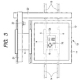
- FIG. 3 is a plan view of the screen-printing apparatus according to the first embodiment of the present invention.
- FIG. 4 is a plan view of a board printing surface by the screen-printing apparatus according to the first embodiment of the present invention.
- FIG. 5 is a block diagram showing the structure of a control system of the screen-printing apparatus according to the first embodiment of the present invention.
- FIG. 6 is a view showing the storage contents of a program storing part and a data storing part of the screen-printing apparatus according to the first embodiment of the present invention.
- FIG. 7 is an explanatory view of element form and position data of element solder printing parts of the screen-printing apparatus according to the first embodiment of the present invention.
- FIG. 8 is a flow chart for a mask plate image pick-up process for forming mask opening data in a method for forming print inspecting data according to the first embodiment of the present invention.
- FIG. 9 is a diagram showing visual field positions upon mask plate image pick-up process in the method for forming print inspecting data according to the first embodiment of the present invention.
- FIG. 10 is an explanatory view of the mask plate image pick-up process in the method for forming print inspecting data according to the first embodiment of the present invention.
- FIG. 11 is an explanatory view of the mask plate image pick-up process in the method for forming print inspecting data according to the first embodiment of the present invention.
- FIG. 12 is an explanatory view of the mask plate image pick-up process in the method for forming print inspecting data according to the first embodiment of the present invention.
- FIG. 13 is a flow chart for a mask plate image pick-up process for forming mask opening data in a method for forming print inspecting data according to a second embodiment of the present invention.
- FIG. 14 is an explanatory view of the mask plate image pick-up process in the method for forming print inspecting data according to the second embodiment of the present invention.
- FIG. 15 is an explanatory view of the mask plate image pick-up process in the method for forming print inspecting data according to the second embodiment of the present invention.
- FIG. 16 is an explanatory view of the mask plate image pick-up process in the method for forming print inspecting data according to the second embodiment of the present invention.
- a mask data obtaining step for obtaining positions or forms of opening parts by picking-up the image of a mask plate
- the image pick-up visual field of a camera is sequentially moved to a plurality of visual field positions set to the mask plate in accordance with a prescribed moving sequence
- an adjacent image pick-up visual field is overlapped on the one image pick-up visual field by an overlap margin determined by the sizes of the incomplete opening parts in the image.
- FIG. 1 is a front view of a screen-printing apparatus according to a first embodiment.
- FIG. 2 is a side view of the screen-printing apparatus according to the first embodiment of the present invention.
- FIG. 3 is a plan view of the screen-printing apparatus according to the first embodiment of the present invention.
- FIG. 4 is a plan view of a board printing surface by the screen-printing apparatus according to the first embodiment of the present invention.
- FIG. 5 is a block diagram showing the structure of a control system of the screen-printing apparatus according to the first embodiment of the present invention.
- FIG. 6 is a view showing the storage contents of a program storing part and a data storing part of the screen-printing apparatus according to the first embodiment of the present invention.
- FIG. 7 is an explanatory view of element form and position data of element solder printing parts of the screen-printing apparatus according to the first embodiment of the present invention.
- FIG. 8 is a flow chart for a mask plate image pick-up process for forming mask opening data in a method for forming printing inspection data according to the first embodiment of the present invention.
- FIG. 9 is a diagram showing a visual field position upon mask plate image pick-up process in the method for forming printing inspection data according to the first embodiment of the present invention.
- FIGS. 10 , 11 and 12 are explanatory views of the mask plate image pick-up process in the method for forming printing inspection data according to the first embodiment of the present invention.
- the screen-printing apparatus has a structure including not only a printing mechanism for printing cream solder on a board on which electronic parts are mounted, but also a function as a printing inspection apparatus for inspecting the printed state of the scream solder on the board after a screen printing, and a function in a printing inspection, as described below, as a printing inspection data forming apparatus for forming inspecting data including form and position data indicating the forms and the positions of solder printing parts on which the cream solder is printed.
- a board positioning part 1 comprises a ⁇ -axis table 4 stacked on a moving table including an X-axis table 2 and a Y-axis table 3 and a Z-axis table 5 further disposed thereon.
- a board holding part 7 for holding a board 6 held by a damper 8 from a lower part is provided on the Z-axis table 5 .
- the board 6 as an object to be printed is conveyed to the board positioning part 1 by a take-in conveyor 14 shown in FIGS. 1 and 3 .
- the board positioning part 1 is driven so that the board 6 is moved to X and Y directions and positioned at a below-described printing position and a board recognizing position.
- a take-out conveyor 15 conveys out the board 6 after the printing operation.
- a screen mask 10 is arranged above the board positioning part 1 .
- a mask plate 12 is mounted on a holder 11 to form the screen mask 10 .
- the board 6 is positioned and abuts on the mask plate 12 from a lower part by the board positioning part 1 .
- electrodes 6 b , 6 c , 6 d and 6 e for connecting together different kinds of electronic parts P 1 , P 2 , P 3 and P 4 are provided as shown in FIG. 4( a ).
- a squeegee head 13 is arranged to freely reciprocate in the horizontal direction. While the board 6 abuts on the lower surface of the mask plate 12 , cream solder 9 is supplied onto the mask plate 12 and the squeegees 13 a of the squeegee head 13 are allowed to abut and slide on the surface of the mask plate 12 , so that the cream solder 9 is printed on the printing surface of the board 6 through pattern holes 16 provided on the mask plate 12 .
- element solder printing parts S 1 , S 2 , S 3 and S 4 are respectively formed on the electrodes 6 b , 6 c , 6 d and 6 e.
- a camera 20 as image pick-up means is provided above the screen mask 10 .
- the camera 20 is horizontally moved in X and Y directions by an X-axis table 21 and a Y-axis table 22 .
- the X-axis table 21 and the Y-axis table 22 are camera moving means for moving the camera 20 .
- the camera 20 is moved relative to the mask plate 12 by the camera moving means so that the camera 20 picks-up the images of arbitrary positions of the mask plate 12 .
- the board positioning part 1 is moved in a Y direction from a lower part of the screen mask 10 by the Y-axis table 3 to move the held board 6 to a board recognizing position.
- the camera 20 is moved to the board 6 on the board positioning part 1 so that the camera 20 can pick-up the images of the arbitrary positions of the board 6 .
- a calculation part 25 is a CPU to perform various kinds of programs stored in a program storing part 26 so that the calculation part 25 performs various kinds of calculations and processes described below. In these calculations and processes, various types of data stored in a data storing part 27 are employed.
- An operation and input part 28 is input means such as a keyboard or a mouse to input various kinds of control commands or data.
- a communication part 29 transmits data to and receives data from other apparatus forming electronic parts mounting line together with the screen printing apparatus.
- An image processing part 30 performs an image process of image data picked-up by the camera 20 to recognize solder printing parts for a printing inspection or detect mask opening parts for forming printing inspection data, as described below.
- a mechanism control part 31 controls the camera moving means for moving the camera 20 or squeegee moving means for moving the squeegee head 13 .
- a display part 32 is a display apparatus and serves as display means for displaying an operating screen in a printing inspection data forming process or the decided result of the print inspection as well as images obtained by the camera 20 .
- the programs and the data respectively stored in the program storing part 26 and the data storing part 27 will be described.
- the various kinds of programs including a printing operation program 26 a , an image processing program 26 b , a program 26 c for deciding whether a print is good or not, a mask plate image pick-up processing program 26 d or the like are stored.
- the printing operation program 26 a is a program for the printing operation for controlling the operations of the board positioning part 1 and the squeegee head 13 to print the cream solder 9 on the board 6 .
- the image processing program 26 b is a program according to which the image processing part 30 carries out two kinds of processes described below based on the image pick-up results of the camera 20 .
- the image pick-up result obtained by picking-up the image of the board 6 after printing is recognized to detect the element solder printing parts (see FIG. 4( b )) respectively formed on the electrodes of the board 6 and calculate the area of each element solder printing part. Further, the image pick-up result obtained by picking-up the image of the mask plate 12 is recognized to detect each pattern hole 16 provided in the mask plate 12 and form mask opening data based on the detected result.
- the program 26 c for deciding whether a print is good or not compares the area of the element solder printing part calculated by the image processing part 30 with an inspection threshold value to decide whether or not the printed state of each element solder printing part is good. That is, a function realized by the image processing part 30 and the calculation part 25 which perform the program 26 c for deciding whether a print is good or not constitutes print deciding means for deciding whether a printed state is good or not on the basis of the image pick-up result of the board and the inspecting data necessary for performing the printing inspection.
- the mask plate image pick-up processing program 26 d is a program for performing a necessary process when the mask plate 12 is divided by a plurality of image pick-up visual fields to pick-up images upon picking-up the image of the mask plate 12 by the camera 20 to prepare the mask opening data. As described below, opening parts showing the pattern holes are prevented from being divided by the boundaries of the image pick-up visual fields by this mask plate image pick-up process.
- mounting data 27 a In the data storing part 27 , mounting data 27 a , a parts data library 27 b and a mask opening data library 27 c are stored.
- the mounting data 27 a , the parts data library 27 b and the mask opening data library 27 c of these data are transferred from other apparatus such as data managing computer through a communication part 29 and stored.
- the mounting data 27 a is data used in a mounting operation for mounting electronic parts on the board on which the cream solder is printed, that is, data in which the kinds of electronic parts to be mounted are associated with mounting position coordinates on the board.
- the parts data library 27 b is data related to individual electronic parts to be mounted on the board.
- the mask opening data library 27 c stores numeric value data showing the opening positions or the sizes of the pattern holes 16 of the mask plate 12 used for printing for many kinds of goods and is previously given as the mask opening data attached to the individual mask plates.
- each pattern hole 16 b or 16 e data of each pattern hole 16 b or 16 e is given.
- dimensions a and b showing the size of the pattern hole or the position coordinate values x 1 , x 2 , x 3 , x 4 . . . , y 1 , y 2 , y 3 , y 4 . . . of each pattern hole 16 b relative to a reference origin are given in the form of numeric value data.
- the same data is given.
- This mask opening data is used as element position and form data showing the positions and forms of the element solder printing parts (S 1 to S 4 ) shown in FIG. 4( b ) in the print inspection.
- the mask opening data is not necessarily prepared as data library for all kinds of boards so that a performer side of the inspection may sometimes need to prepare the mask opening data.
- the image of the actual mask plate 12 is picked-up by the camera 20 to form the mask opening data.
- a process for obtaining element form and position data (a mask data obtaining step), is carried out, which shows the forms and positions of the element solder printing parts printed on the electrodes for connecting electronic parts provided on the circuit forming surface of the board by detecting the opening parts of the mask plate based on the images got by picking-up the image of the mask plate used for the screen printing by the camera.
- FIG. 9 the arrangement of visual field positions set to the mask plate 12 is described.
- the printing range of the mask plate 12 whose image is to be picked-up is larger than the image pick-up visual field of the camera 20 . Accordingly, when the image of one mask plate is picked-up, the image needs to be picked-up a plurality of times while the position of the image pick-up visual field of the camera 20 is sequentially shifted. Therefore, when the image of the mask plate is picked-up, visual field positions as target positions where the image pick-up visual field moves are previously set to the mask plate on the basis of a visual field size.
- a plurality of visual field positions [ 1 ], [ 2 ], [ 3 ], [ 4 ], [ 5 ] and [ 6 ] are set in a grid shaped arrangement having two rows and three columns. That is, the visual field positions are set in the grid shaped arrangement having rows combined with columns.
- [ 1 ] and [ 2 ] form a first column
- [ 3 ] and [ 4 ] form a second column
- [ 5 ] and [ 6 ] form a third column.
- the image pick-up visual field 20 a of the camera 20 is sequentially moved to these visual field positions in a prescribed moving sequence to obtain a plurality of images. Accordingly, a necessary image pick-up range can be completely covered.
- the prescribed moving sequence is a moving sequence performed in such a manner that a linear column movement (from an upper side to a lower side in FIG. 9 ) toward the same direction from a start end side to a terminal end side of a first direction (Y direction) in the grid-shaped arrangement is repeated for each column in a second direction (X direction) perpendicular to the first direction.
- grid shaped broken lines show visual field boundaries when the image pick-up visual filed 20 a of the camera 20 is located in these visual fields.
- the visual field boundaries may sometimes traverse the pattern holes. This means a fact that when the image pick-up visual field is simply moved to these visual field positions to pick-up the image, an opening part showing one pattern hole is detected over a plurality of images.
- the positions or the forms of the opening parts to which incomplete opening parts detected in their divided forms belong are obtained by a method described below.
- the camera 20 is moved on the mask plate 12 to move the image pick-up visual field 20 a to a target visual field position (ST 1 ).
- the first visual field position [ 1 ] is a first object whose image is to be picked-up.
- the image of this image pick-up visual field is obtained by the camera 20 (ST 2 ) to recognize the obtained image (ST 3 ).
- an image 20 b shown in FIG. 10( b ) is obtained and the-pattern holes 16 b in the image pick-up visual field are detected as the opening parts.
- incomplete opening parts 16 b (Y) are detected in the lower boundary side in the image 20 b .
- the size BY 1 of the detected incomplete opening parts 16 b (Y) in the direction of Y is obtained on the image.
- the range of a width size BY 2 obtained by adding a prescribed margin to the BY 1 is considered to be a data formation excluding range (see oblique line hatching parts).
- the width size BY 2 is determined to be an overlap margin in the direction Y in a next visual field (ST 11 ) and the procedure returns to (ST 1 ).
- the image pick-up visual field 20 a is moved to the visual field position [ 2 ] as a next object.
- the visual field 20 a is not directly moved by a visual field size in the direction of Y, and the visual field 20 a is overlapped by the BY 2 determined as the overlap margin in the direction of Y on the image pick-up visual field in the previous visual field position. That is, the overlap margin in the direction of Y is determined based on the size of the incomplete opening parts in the direction of Y in the image.
- the image 20 b in which the pattern holes 16 b , which are the incomplete opening parts on the image obtained in the visual field position [ 1 ], are completely included is obtained.
- the same processes are performed on the image 20 b .
- incomplete opening parts 16 d (X) corresponding to pattern holes 16 d are detected in the right boundary side in the image 20 b .
- the size DX 1 of the incomplete opening parts 16 d (X) in the direction of X is obtained on the image.
- the range of a width size DX 2 is likewise determined to be a data formation excluding range (see oblique line hatching lines) and stored.
- the procedure advances to (ST 7 ) to determine the maximum value of the sizes of the data formation excluding ranges in the image pick-up visual fields in this column as an overlap margin in the direction of X. That is, the larger size of the width sizes BX 2 and DX 2 of the data formation excluding ranges in the direction of X in the visual fields in the visual field positions [ 1 ] and [ 2 ] is determined as the overlap margin in the direction of X upon change of a column position.
- the BX 2 is larger than the DX 2
- the BX 2 is determined as the overlap margin in the direction of X.
- the column position is changed (ST 8 ).
- the image pick-up visual field 20 a is moved to the visual field position [ 3 ] of a second column.
- the visual field 20 a is not moved by a visual field size in the direction of X, and overlapped by the BX 2 determined as the overlap margin in the direction of X on the image pick-up visual field in the visual field position of a first column.
- the overlap margin in the direction of X (second direction) in which two adjacent image pick-up visual fields are overlapped in the direction of X is set based on the maximum size of sizes of the incomplete opening parts in the direction of X detected in the first column movement. Then, in a column movement subsequent to the first column movement, the same overlap margin in the direction of X is used for all the visual field positions.
- the image 20 b in which the pattern holes 16 b , which are the incomplete opening parts on the image obtained in the visual field position [ 1 ], are completely included is obtained.
- the same processes are performed for the image 20 b .
- the incomplete opening parts are not detected in the image 20 b , data formation excluding ranges are not set both in the directions of X and Y.
- the procedure returns to the (ST 1 ) to move the image pick-up visual field.
- the image pick-up visual field 20 a is directly moved to the visual field position [ 4 ] shown in FIG. 12( a ).
- the image 20 b in which pattern holes 16 d , which are the incomplete opening parts on the image obtained in the visual field position [ 2 ], are completely included is obtained. Then, the same processes are performed for this image 20 b.
- the image pick-up visual field 20 a of the camera 20 is sequentially moved to the plural visual field positions set to the mask plate 12 in a prescribed moving sequence to obtain a plurality of images, if the incomplete opening parts in which parts of the opening parts partly protrude from the image obtained in one image pick-up visual field and the forms are not completed are detected, the adjacent image pick-up visual field in the end of the image in which the incomplete opening parts are detected is overlapped by the overlap margin determined based on the size of the incomplete opening parts in the image on the one image pick-up visual field.
- the mask opening data can be simply and efficiently obtained to form the inspecting data without increasing a processing load or generating the deterioration of detection accuracy due to the fragmentation of the opening parts on the image.
- the mask data obtaining step for picking-up the image of the mask plate to obtain the positions or the forms of the opening parts when the image pick-up visual field of the camera is sequentially moved to the plural visual field positions set to the mask plate in accordance with a prescribed moving sequence, if the incomplete opening parts which partly protrude from the image obtained in one image pick-up visual field are detected, the adjacent image pick-up visual field is overlapped by the overlap margin determined based on the size of the incomplete opening parts in the image on the one image pick-up visual field to pick-up the image.
- a mask data obtaining step for obtaining the forms or configurations and the positions of opening parts by picking-up the image of a mask plate
- the image pick-up visual field of a camera is sequentially moved to a plurality of visual field positions set to the mask plate in accordance with a prescribed moving sequence
- a connecting process is carried out in which an opening part to be connected that is already registered in an image obtained in an adjacent image pick-up visual field on an edge of an image where the opening part to be connected is detected and corresponds to the opening part to be connected is connected to the opening part to be connected to form one opening part.
- FIG. 13 is a flowchart of a mask plate image pick-up process for forming mask opening data in a method for forming printing inspection data according to the second embodiment of the present invention.
- FIGS. 14 , 15 and 16 are explanatory views of the mask plate image pick-up process in the method for forming print inspecting data according to the second embodiment of the present invention.
- a camera 20 is moved to the mask plate 12 to move an image pick-up visual field 20 a to a target visual field position (ST 1 ).
- the first visual field position [ 1 ] shown in FIG. 9 is a first object whose image is to be picked-up.
- the image of this image pick-up visual field is obtained by the camera 20 (ST 2 ) to recognize the obtained image (ST 3 ).
- an image 20 b shown in FIG. 14( a ) is obtained and pattern holes 16 b in the image pick-up visual field are detected as the opening parts.
- the incomplete opening parts 16 b (X) corresponding to the pattern holes 16 b are detected in the right boundary side in the image 20 b . Then, the forms of the incomplete opening parts 16 b (X) (here, rectangular shapes) are decided and y 11 , y 12 and y 13 as positions in the direction of Y are obtained on the image to store these data.
- the positions of opening parts to be connected are located in a left side in the visual field, a process is carried out for connecting opening parts to be connected which are already registered in an adjacent image pick-up visual field of a previous column to the opening parts to be connected which are registered in the image of the image pick-up visual field.
- the visual field position [ 1 ] is in a first column, the previous column does not exist. Accordingly, the connecting process is not performed.
- the incomplete opening parts 16 b (Y) corresponding to the pattern holes 16 b are detected in the lower side in the image 20 b . Then, the configurations of the incomplete opening parts 16 b (Y) are decided and positions x 11 , x 12 and x 13 in the direction of X are obtained on the image to store these data.
- a connecting process is carried out in which opening parts to be connected that are already registered in a previous image pick-up visual field are connected to the opening parts to be connected that are registered in the image of this image pick-up visual field.
- the connecting process is not carried out since the incomplete opening parts 16 b (Y) are detected only in the lower edge side.
- the procedure returns to the (ST 1 ) to move the image pick-up visual field 20 a to the visual field [ 2 ] as a next object and repeat the steps after the (ST 2 ).
- an image shown in FIG. 14( b ) is obtained and incomplete opening parts 16 d (X) in the direction of X are detected in a right edge side and incomplete opening parts 16 b (Y) in the direction of Y are detected in an upper edge side.
- these incomplete opening parts 16 d (X) and 16 b (Y) are registered as opening parts to be connected to store respectively the configurations or forms and positions x 21 , x 22 , x 23 , y 21 and y 22 thereof.
- a connecting process is performed in (ST 11 ) in which the incomplete opening parts 16 b (Y) are connected to the opening parts to be connected that are already registered in the previous image pick-up visual field. That is, as shown in FIG. 15( a ), the incomplete opening parts 16 b (Y) included in the image in the visual field position [ 1 ] are butted and connected onto the incomplete opening parts 16 b (Y) included in the image in the image pick-up visual field [ 2 ].
- the two incomplete opening parts obtained in the separate images are connected together to form the opening parts 16 b (pattern holes) whose configurations are completed on the image.
- the opening parts 16 b pattern holes
- data showing sizes a and b and a central position C (x, y) of each opening part 16 is obtained which have been incapable of being detected in the original images obtained by picking-up the images respectively in the visual fields.
- the data of the opening parts in which these connecting processes are performed is combined with the data of the opening parts individually detected in the respective images to obtain the mask opening data shown in FIG. 7 .
- the central positions of the incomplete opening parts do not usually correspond to each other.
- the positions x 13 and x 23 in the direction of X do not sometimes correspond to each other.
- the average position xm of the positions x 13 and x 23 is obtained as a central point of dislocation and the two incomplete opening parts are respectively moved to the central point of dislocation. That is, in this connecting process, when the opening part to be connected is dislocated from the opening part to be connected that corresponds thereto and is already registered, both the opening parts are respectively moved by half an amount of dislocation toward the central point of dislocation.
- the procedure returns again to the (ST 1 ) to move the image pick-up visual field 20 a to a visual field position as a next object and repeat the same processes.
- images shown in FIGS. 16( a ) and 16 ( b ) are obtained.
- a connecting process is carried out in which the opening parts 16 b (X) to be connected in the direction of X that are already detected and registered in the visual field position [ 1 ] are butted and connected to the opening parts 16 b (X) to be connected in the direction of X are detected and registered in the visual field position [ 3 ].
- a connecting process is carried out in which the opening parts 16 d (X) to be connected in the direction of X that are already detected and registered in the visual field position [ 2 ] are butted and connected onto the opening parts 16 d (X) to be connected in the direction of X that are detected and registered in the visual field position [ 4 ]. Then, after that, the same image pick-up processes are performed in the visual field positions [ 5 ] and [ 6 ], so that the image pick-up processes for the mask plate 12 as a target are completed.
- a connecting process is carried out in which the opening parts to be connected that are already registered in the image obtained in the adjacent image pick-up visual filed in the edge of the image in which the opening parts to be connected are detected and correspond to the opening parts to be connected are searched, and the opening parts to be connected that are already registered are connected to the opening parts to be connected to form complete openings respectively.
- the image pick-up visual field is moved on the mask plate to pick-up the images a plurality of times, even if the opening parts may possibly partly protrude from the image pick-up visual field in one visual field position, the corresponding incomplete opening parts are properly butted and connected onto the above-described opening parts. Consequently, the positions and forms of the opening parts can be precisely obtained so that the mask opening data can be simply and efficiently obtained to form the inspecting data.
- the mask data obtaining step for obtaining the positions or the configurations of the opening parts by picking-up the image of the mask plate when the image pick-up visual field of the camera is sequentially moved to a plurality of visual field positions set to the mask plate in a prescribed moving sequence, if the incomplete opening parts partly protruding from the image obtained in one image pick-up visual field are detected, the incomplete opening parts are registered as the opening parts to be connected in this image, and then, a connecting process is carried out in which the opening parts to be connected that are already registered in the image obtained in the adjacent image pick-up visual filed in the edge of the image in which the opening parts to be connected are detected and correspond to the opening parts to be connected are connected to the opening parts to be connected to form complete openings respectively. Accordingly, the-inspecting data can be simply and efficiently formed.
- the mask data obtaining step for obtaining the positions or the configurations of the opening parts by picking-up the image of the mask plate when the image pick-up visual field of the camera is sequentially moved to a plurality of visual field positions set to the mask plate in a prescribed moving sequence, if the incomplete opening parts partly protruding from the image obtained in one image pick-up visual field are detected, a process for obtaining the complete opening parts to which the incomplete opening parts belong is performed based on the detected result. Therefore, the inspecting data can be simply and efficiently formed.
Landscapes
- Engineering & Computer Science (AREA)
- Analytical Chemistry (AREA)
- General Health & Medical Sciences (AREA)
- Pathology (AREA)
- Physics & Mathematics (AREA)
- Health & Medical Sciences (AREA)
- Life Sciences & Earth Sciences (AREA)
- Chemical & Material Sciences (AREA)
- Immunology (AREA)
- Biochemistry (AREA)
- General Physics & Mathematics (AREA)
- Microelectronics & Electronic Packaging (AREA)
- Manufacturing & Machinery (AREA)
- Quality & Reliability (AREA)
- Electric Connection Of Electric Components To Printed Circuits (AREA)
- Image Processing (AREA)
- Investigating Materials By The Use Of Optical Means Adapted For Particular Applications (AREA)
- Screen Printers (AREA)
Abstract
Description
Claims (7)
Applications Claiming Priority (4)
| Application Number | Priority Date | Filing Date | Title |
|---|---|---|---|
| JP2002238089A JP4100089B2 (en) | 2002-08-19 | 2002-08-19 | How to create print inspection data |
| JPP.2002-238089 | 2002-08-19 | ||
| JPP.2002-238088 | 2002-08-19 | ||
| JP2002238088A JP4048876B2 (en) | 2002-08-19 | 2002-08-19 | How to create print inspection data |
Publications (2)
| Publication Number | Publication Date |
|---|---|
| US20040031406A1 US20040031406A1 (en) | 2004-02-19 |
| US6951175B2 true US6951175B2 (en) | 2005-10-04 |
Family
ID=31719889
Family Applications (1)
| Application Number | Title | Priority Date | Filing Date |
|---|---|---|---|
| US10/642,930 Expired - Fee Related US6951175B2 (en) | 2002-08-19 | 2003-08-18 | Method for forming printing inspection data |
Country Status (6)
| Country | Link |
|---|---|
| US (1) | US6951175B2 (en) |
| EP (2) | EP1677584B1 (en) |
| KR (1) | KR100990968B1 (en) |
| AU (1) | AU2003260948A1 (en) |
| DE (2) | DE60306389T2 (en) |
| WO (1) | WO2004017703A2 (en) |
Families Citing this family (10)
| Publication number | Priority date | Publication date | Assignee | Title |
|---|---|---|---|---|
| JP4379348B2 (en) * | 2005-02-15 | 2009-12-09 | パナソニック株式会社 | Electronic component mounting system and electronic component mounting method |
| US8167661B2 (en) | 2008-12-02 | 2012-05-01 | Panduit Corp. | Method and system for improving crosstalk attenuation within a plug/jack connection and between nearby plug/jack combinations |
| US8493409B2 (en) * | 2009-08-18 | 2013-07-23 | Behavioral Recognition Systems, Inc. | Visualizing and updating sequences and segments in a video surveillance system |
| GB201005750D0 (en) * | 2010-04-06 | 2010-05-19 | Dtg Int Gmbh | Screen printing machine and method |
| JP5523300B2 (en) | 2010-12-24 | 2014-06-18 | 富士機械製造株式会社 | Substrate production line and inspection machine data generation method |
| US20160057855A1 (en) * | 2013-04-15 | 2016-02-25 | Heptagon Micro Optics Pte. Ltd. | Accurate Positioning and Alignment of a Component During Processes Such as Reflow Soldering |
| CN103252983B (en) * | 2013-05-31 | 2016-02-03 | 中利腾晖光伏科技有限公司 | A kind of grid line printing equipment |
| JP6272676B2 (en) * | 2013-11-07 | 2018-01-31 | 東レエンジニアリング株式会社 | Bonding equipment |
| KR102528016B1 (en) * | 2018-10-05 | 2023-05-02 | 삼성전자주식회사 | Solder member mounting method and system |
| CN116500050B (en) * | 2023-06-28 | 2024-01-12 | 四川托璞勒科技有限公司 | PCB visual inspection system |
Citations (10)
| Publication number | Priority date | Publication date | Assignee | Title |
|---|---|---|---|---|
| EP0563829A2 (en) * | 1992-03-30 | 1993-10-06 | Sharp Kabushiki Kaisha | Device for inspecting printed cream solder |
| DE19728144A1 (en) | 1997-07-02 | 1999-01-07 | Ekra Eduard Kraft Gmbh | Method and device for generating test patterns |
| US5912984A (en) | 1996-12-19 | 1999-06-15 | Cognex Corporation | Method and apparatus for in-line solder paste inspection |
| US5991435A (en) * | 1992-06-30 | 1999-11-23 | Matsushita Electric Industrial Co., Ltd. | Inspecting apparatus of mounting state of component or printing state of cream solder in mounting line of electronic component |
| US6088109A (en) * | 1998-09-24 | 2000-07-11 | Advanced Semiconductor Engineering, Inc. | System for detecting the presence of deposited metals on soldering points of an integrated circuit board substrate |
| EP1048946A2 (en) | 1999-04-27 | 2000-11-02 | Matsushita Electric Industrial Co., Ltd. | Inspection method and device |
| JP2002029033A (en) | 2000-07-18 | 2002-01-29 | Matsushita Electric Ind Co Ltd | Method for creating data for inspection of print inspecting device |
| US6634290B1 (en) * | 1999-08-10 | 2003-10-21 | Fuji Machine Mfg. Co., Ltd. | Mask-printing apparatus and method including inspection of printed material and re-printing step |
| US6665066B2 (en) * | 2001-04-27 | 2003-12-16 | National Instruments Corporation | Machine vision system and method for analyzing illumination lines in an image to determine characteristics of an object being inspected |
| US6750899B1 (en) * | 2000-01-07 | 2004-06-15 | Cyberoptics Corporation | Solder paste inspection system |
Family Cites Families (2)
| Publication number | Priority date | Publication date | Assignee | Title |
|---|---|---|---|---|
| KR980007918A (en) | 1996-06-29 | 1998-03-30 | 배순훈 | A method of creating a self-contained path and a method of generating the self-contained path |
| JP3832062B2 (en) * | 1997-12-22 | 2006-10-11 | 松下電器産業株式会社 | Cream solder appearance inspection method |
-
2003
- 2003-08-13 AU AU2003260948A patent/AU2003260948A1/en not_active Abandoned
- 2003-08-13 EP EP06003519A patent/EP1677584B1/en not_active Expired - Lifetime
- 2003-08-13 WO PCT/JP2003/010311 patent/WO2004017703A2/en active IP Right Grant
- 2003-08-13 DE DE60306389T patent/DE60306389T2/en not_active Expired - Lifetime
- 2003-08-13 DE DE60316998T patent/DE60316998T2/en not_active Expired - Lifetime
- 2003-08-13 KR KR1020057002686A patent/KR100990968B1/en not_active IP Right Cessation
- 2003-08-13 EP EP03788103A patent/EP1532850B1/en not_active Expired - Lifetime
- 2003-08-18 US US10/642,930 patent/US6951175B2/en not_active Expired - Fee Related
Patent Citations (12)
| Publication number | Priority date | Publication date | Assignee | Title |
|---|---|---|---|---|
| EP0563829A2 (en) * | 1992-03-30 | 1993-10-06 | Sharp Kabushiki Kaisha | Device for inspecting printed cream solder |
| US5450204A (en) * | 1992-03-30 | 1995-09-12 | Sharp Kabushiki Kaisha | Inspecting device for inspecting printed state of cream solder |
| US5991435A (en) * | 1992-06-30 | 1999-11-23 | Matsushita Electric Industrial Co., Ltd. | Inspecting apparatus of mounting state of component or printing state of cream solder in mounting line of electronic component |
| US6167149A (en) * | 1992-06-30 | 2000-12-26 | Matsushita Electric Industrial Co. | Inspecting apparatus of mounting state of component or printing state of cream solder in mounting line of electronic component |
| US5912984A (en) | 1996-12-19 | 1999-06-15 | Cognex Corporation | Method and apparatus for in-line solder paste inspection |
| DE19728144A1 (en) | 1997-07-02 | 1999-01-07 | Ekra Eduard Kraft Gmbh | Method and device for generating test patterns |
| US6088109A (en) * | 1998-09-24 | 2000-07-11 | Advanced Semiconductor Engineering, Inc. | System for detecting the presence of deposited metals on soldering points of an integrated circuit board substrate |
| EP1048946A2 (en) | 1999-04-27 | 2000-11-02 | Matsushita Electric Industrial Co., Ltd. | Inspection method and device |
| US6634290B1 (en) * | 1999-08-10 | 2003-10-21 | Fuji Machine Mfg. Co., Ltd. | Mask-printing apparatus and method including inspection of printed material and re-printing step |
| US6750899B1 (en) * | 2000-01-07 | 2004-06-15 | Cyberoptics Corporation | Solder paste inspection system |
| JP2002029033A (en) | 2000-07-18 | 2002-01-29 | Matsushita Electric Ind Co Ltd | Method for creating data for inspection of print inspecting device |
| US6665066B2 (en) * | 2001-04-27 | 2003-12-16 | National Instruments Corporation | Machine vision system and method for analyzing illumination lines in an image to determine characteristics of an object being inspected |
Non-Patent Citations (1)
| Title |
|---|
| Patent Abstracts of Japan, Sakaguchi Hiroyuki, "Apparatus and Method for Visual Inspection of Cream Solder", Publication No.: 11186711, Publication Date Jul. 9, 1999, 1 page. |
Also Published As
| Publication number | Publication date |
|---|---|
| DE60316998T2 (en) | 2008-02-14 |
| EP1532850B1 (en) | 2006-06-21 |
| DE60306389D1 (en) | 2006-08-03 |
| WO2004017703A3 (en) | 2004-05-27 |
| KR100990968B1 (en) | 2010-10-29 |
| DE60316998D1 (en) | 2007-11-29 |
| US20040031406A1 (en) | 2004-02-19 |
| DE60306389T2 (en) | 2006-10-19 |
| WO2004017703A2 (en) | 2004-02-26 |
| AU2003260948A1 (en) | 2004-03-03 |
| EP1677584A2 (en) | 2006-07-05 |
| EP1532850A2 (en) | 2005-05-25 |
| AU2003260948A8 (en) | 2004-03-03 |
| KR20050033649A (en) | 2005-04-12 |
| EP1677584A3 (en) | 2006-07-26 |
| EP1677584B1 (en) | 2007-10-17 |
Similar Documents
| Publication | Publication Date | Title |
|---|---|---|
| CN1318839C (en) | Automatic optical detecting system for blemish assembly on printed circuit board | |
| US11176635B2 (en) | Automatic programming of solder paste inspection system | |
| US6951175B2 (en) | Method for forming printing inspection data | |
| JP2007184450A (en) | Mounting system and method of mounting electronic component | |
| JP2011082243A (en) | Component mounting device, and mounting-state inspection method in the same | |
| JP2776860B2 (en) | Electronic component mounting device and mounting method | |
| JP6830538B2 (en) | Board work management system | |
| WO2017081773A1 (en) | Image processing device and image processing method for base plate | |
| WO2017072908A1 (en) | Base plate position searching device and component mounting machine | |
| JP2004095978A (en) | Method and system for contra-substrate working | |
| JP4782590B2 (en) | Component mounting position teaching method | |
| JP4048876B2 (en) | How to create print inspection data | |
| JP2000211106A (en) | Screen mask aligning method in screen printing | |
| JP2942343B2 (en) | Inspection equipment for printed wiring boards | |
| JP4082120B2 (en) | Printing inspection simulation apparatus and printing inspection simulation method | |
| US5975742A (en) | Electronic part inserting apparatus with checking function for clinched state, and checking method thereof | |
| JP4554190B2 (en) | Printing inspection apparatus and printing inspection method | |
| KR20000056739A (en) | Inspecting apparatus for pcb and teaching method and library modifying method thereof | |
| JPH1140999A (en) | Electronic component mounting method on multiply formed boards | |
| JP3566908B2 (en) | Inspection method and inspection device | |
| JP2005164457A (en) | Data generation device for visual inspection, and data generation method for visual inspection | |
| JP2573788Y2 (en) | Printed board appearance inspection device | |
| JP2004074578A (en) | Printing checking data forming method | |
| US20200410663A1 (en) | Electronic component mounting orientation checking system and electronic component mounting orientation checking method | |
| JPH0464291A (en) | Mounting method for electronic component |
Legal Events
| Date | Code | Title | Description |
|---|---|---|---|
| AS | Assignment |
Owner name: MATSUSHITA ELECTRIC INDUSTRIAL CO., LTD., JAPAN Free format text: ASSIGNMENT OF ASSIGNORS INTEREST;ASSIGNORS:OTAKE, YUJI;FUKAGAWA, TAKAHIRO;KATSUKI, TAKASHI;REEL/FRAME:014407/0345 Effective date: 20030728 |
|
| FEPP | Fee payment procedure |
Free format text: PAYOR NUMBER ASSIGNED (ORIGINAL EVENT CODE: ASPN); ENTITY STATUS OF PATENT OWNER: LARGE ENTITY |
|
| FEPP | Fee payment procedure |
Free format text: PAYOR NUMBER ASSIGNED (ORIGINAL EVENT CODE: ASPN); ENTITY STATUS OF PATENT OWNER: LARGE ENTITY Free format text: PAYER NUMBER DE-ASSIGNED (ORIGINAL EVENT CODE: RMPN); ENTITY STATUS OF PATENT OWNER: LARGE ENTITY |
|
| FPAY | Fee payment |
Year of fee payment: 4 |
|
| FPAY | Fee payment |
Year of fee payment: 8 |
|
| AS | Assignment |
Owner name: GODO KAISHA IP BRIDGE 1, JAPAN Free format text: ASSIGNMENT OF ASSIGNORS INTEREST;ASSIGNOR:PANASONIC CORPORATION (FORMERLY MATSUSHITA ELECTRIC INDUSTRIAL CO., LTD.);REEL/FRAME:032209/0630 Effective date: 20131203 |
|
| REMI | Maintenance fee reminder mailed | ||
| LAPS | Lapse for failure to pay maintenance fees |
Free format text: PATENT EXPIRED FOR FAILURE TO PAY MAINTENANCE FEES (ORIGINAL EVENT CODE: EXP.) |
|
| STCH | Information on status: patent discontinuation |
Free format text: PATENT EXPIRED DUE TO NONPAYMENT OF MAINTENANCE FEES UNDER 37 CFR 1.362 |
|
| FP | Lapsed due to failure to pay maintenance fee |
Effective date: 20171004 |