US6546030B2 - Semiconductor laser unit employing an inorganic adhesive - Google Patents
Semiconductor laser unit employing an inorganic adhesive Download PDFInfo
- Publication number
- US6546030B2 US6546030B2 US09/892,510 US89251001A US6546030B2 US 6546030 B2 US6546030 B2 US 6546030B2 US 89251001 A US89251001 A US 89251001A US 6546030 B2 US6546030 B2 US 6546030B2
- Authority
- US
- United States
- Prior art keywords
- semiconductor laser
- laser unit
- fixation
- inorganic adhesive
- inorganic
- Prior art date
- Legal status (The legal status is an assumption and is not a legal conclusion. Google has not performed a legal analysis and makes no representation as to the accuracy of the status listed.)
- Expired - Lifetime
Links
Images


Classifications
-
- H—ELECTRICITY
- H01—ELECTRIC ELEMENTS
- H01S—DEVICES USING THE PROCESS OF LIGHT AMPLIFICATION BY STIMULATED EMISSION OF RADIATION [LASER] TO AMPLIFY OR GENERATE LIGHT; DEVICES USING STIMULATED EMISSION OF ELECTROMAGNETIC RADIATION IN WAVE RANGES OTHER THAN OPTICAL
- H01S5/00—Semiconductor lasers
- H01S5/02—Structural details or components not essential to laser action
- H01S5/022—Mountings; Housings
- H01S5/0235—Method for mounting laser chips
- H01S5/02355—Fixing laser chips on mounts
- H01S5/0236—Fixing laser chips on mounts using an adhesive
-
- H—ELECTRICITY
- H01—ELECTRIC ELEMENTS
- H01S—DEVICES USING THE PROCESS OF LIGHT AMPLIFICATION BY STIMULATED EMISSION OF RADIATION [LASER] TO AMPLIFY OR GENERATE LIGHT; DEVICES USING STIMULATED EMISSION OF ELECTROMAGNETIC RADIATION IN WAVE RANGES OTHER THAN OPTICAL
- H01S5/00—Semiconductor lasers
- H01S5/02—Structural details or components not essential to laser action
- H01S5/022—Mountings; Housings
- H01S5/0225—Out-coupling of light
- H01S5/02251—Out-coupling of light using optical fibres
-
- H—ELECTRICITY
- H01—ELECTRIC ELEMENTS
- H01S—DEVICES USING THE PROCESS OF LIGHT AMPLIFICATION BY STIMULATED EMISSION OF RADIATION [LASER] TO AMPLIFY OR GENERATE LIGHT; DEVICES USING STIMULATED EMISSION OF ELECTROMAGNETIC RADIATION IN WAVE RANGES OTHER THAN OPTICAL
- H01S5/00—Semiconductor lasers
- H01S5/02—Structural details or components not essential to laser action
- H01S5/022—Mountings; Housings
- H01S5/02208—Mountings; Housings characterised by the shape of the housings
-
- H—ELECTRICITY
- H01—ELECTRIC ELEMENTS
- H01S—DEVICES USING THE PROCESS OF LIGHT AMPLIFICATION BY STIMULATED EMISSION OF RADIATION [LASER] TO AMPLIFY OR GENERATE LIGHT; DEVICES USING STIMULATED EMISSION OF ELECTROMAGNETIC RADIATION IN WAVE RANGES OTHER THAN OPTICAL
- H01S5/00—Semiconductor lasers
- H01S5/02—Structural details or components not essential to laser action
- H01S5/022—Mountings; Housings
- H01S5/023—Mount members, e.g. sub-mount members
- H01S5/02325—Mechanically integrated components on mount members or optical micro-benches
-
- H—ELECTRICITY
- H01—ELECTRIC ELEMENTS
- H01S—DEVICES USING THE PROCESS OF LIGHT AMPLIFICATION BY STIMULATED EMISSION OF RADIATION [LASER] TO AMPLIFY OR GENERATE LIGHT; DEVICES USING STIMULATED EMISSION OF ELECTROMAGNETIC RADIATION IN WAVE RANGES OTHER THAN OPTICAL
- H01S5/00—Semiconductor lasers
- H01S5/02—Structural details or components not essential to laser action
- H01S5/024—Arrangements for thermal management
- H01S5/02407—Active cooling, e.g. the laser temperature is controlled by a thermo-electric cooler or water cooling
- H01S5/02415—Active cooling, e.g. the laser temperature is controlled by a thermo-electric cooler or water cooling by using a thermo-electric cooler [TEC], e.g. Peltier element
-
- H—ELECTRICITY
- H01—ELECTRIC ELEMENTS
- H01S—DEVICES USING THE PROCESS OF LIGHT AMPLIFICATION BY STIMULATED EMISSION OF RADIATION [LASER] TO AMPLIFY OR GENERATE LIGHT; DEVICES USING STIMULATED EMISSION OF ELECTROMAGNETIC RADIATION IN WAVE RANGES OTHER THAN OPTICAL
- H01S5/00—Semiconductor lasers
- H01S5/02—Structural details or components not essential to laser action
- H01S5/024—Arrangements for thermal management
- H01S5/02438—Characterized by cooling of elements other than the laser chip, e.g. an optical element being part of an external cavity or a collimating lens
-
- H—ELECTRICITY
- H01—ELECTRIC ELEMENTS
- H01S—DEVICES USING THE PROCESS OF LIGHT AMPLIFICATION BY STIMULATED EMISSION OF RADIATION [LASER] TO AMPLIFY OR GENERATE LIGHT; DEVICES USING STIMULATED EMISSION OF ELECTROMAGNETIC RADIATION IN WAVE RANGES OTHER THAN OPTICAL
- H01S5/00—Semiconductor lasers
- H01S5/02—Structural details or components not essential to laser action
- H01S5/024—Arrangements for thermal management
- H01S5/02476—Heat spreaders, i.e. improving heat flow between laser chip and heat dissipating elements
Definitions
- the present invention relates to a semiconductor laser unit, and more particularly to a semiconductor laser unit having a semiconductor element, optical components, temperature sensing components, etc., within a package.
- an organic adhesive such as epoxy, silicon, etc.
- a temperature sensing component such as a Peltier element, a thermistor, etc.
- an optical component such as a lens, an optical fiber, etc.
- a method of sealing the package hermetically with dried air or inert gas is adapted with the object of preventing condensation within the package or preventing the entrance of dust into the package.
- solder 16 is used in joining a laser stem 14 , bonding a semiconductor laser 15 , and a heat spreader 13 together to assure conductivity and heat radiation.
- the join between other temperature sensing components that require no conductivity is performed by use of an organic adhesive 24 such as epoxy, silicon, etc.
- the organic adhesive used for fixation of the aforementioned components generates organic gases gradually from the interior of the adhesive because of heat generation during laser operation, elapse of time, etc. Since the semiconductor laser unit is in a hermetically sealed state, the generated organic gases adhere to the lens or windowpane and change their transmission factors.
- the present invention has been made in view of the aforementioned circumstances. Accordingly, it is the primary object of the present invention to provide a semiconductor laser unit which is capable of preventing a change in the transmission factor of an optical component and a reduction in the optical output due to the adhesion of a residual organic substance, etc., to the optical component, and obtaining an optical output whose reliability is high up to high output.
- a semiconductor laser unit comprising: a semiconductor laser chip mounted within a package; a temperature sensing component fixed within the package; and an optical component fixed within the package; wherein at least either the fixation of the temperature sensing component or the fixation of the optical component is performed with an inorganic adhesive.
- the package may be hermetically sealed. It is desirable that the inorganic adhesive have at least one of alumina, zirconia, or silica as its main component. It is also desirable that the inorganic adhesive have an inorganic metal material as its main component. In that case it is desirable that the inorganic metal material be soldering material.
- the aforementioned “temperature sensing component” is a component for sensing heat generated from a semiconductor chip or an optical component and then keeping the temperature of the semiconductor chip constant.
- the temperature sensing component has function such as cooling, heat radiation, heating, etc., or has a combined function of them and is fixed within the package along with the optical component.
- optical component refers to any optical component, which is used for light transmission, focusing, polarization, deflection, modulation, wavelength selection, wavelength conversion, etc., such as a lens, an optical filter, etc.
- the optical component used in the present invention includes a windowpane provided in a package cover.
- the aforementioned “inorganic adhesive” is an adhesive composed mainly of an inorganic substance. More specifically, it contains an inorganic substance of 99% or greater and an organic substance of 1% or less.
- main component indicates a component whose content is largest. In the case where there are a plurality of components whose content is almost largest, the main component indicates the plurality of components.
- the present invention is capable of preventing a change in the transmission factor of the optical component, a reduction in optical output, and occurrence of optical noise due to the adhesion of organic gases to the optical component, and obtaining an optical output whose reliability is high up to high output.
- the present invention is also capable of enhancing optical output more effectively if it is applied to a semiconductor laser unit where a package is hermetically sealed.
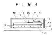
- FIG. 1 is a sectional view showing a semiconductor laser unit constructed according to a first embodiment of the present invention
- FIG. 2 is a sectional view showing a semiconductor laser unit constructed according to a second embodiment of the present invention.
- FIG. 3 is a sectional view showing a semiconductor laser unit constructed according to a third embodiment of the present invention.
- FIG. 4 is a graph showing the quantities of organic gases generated from an organic adhesive and an inorganic adhesive by heating under vacuum;
- FIG. 5 is a graph showing a change in optical output with elapse of time in the case where the semiconductor laser unit of the first embodiment employs an inorganic adhesive and the case where it employs an organic adhesive;
- FIG. 6 is a sectional view showing a conventional semiconductor laser unit employing an organic adhesive.
- a semiconductor laser unit in a first embodiment of the present invention includes Peltier elements 12 stuck within a package 11 with an inorganic adhesive 17 , a heat spreader 13 stuck on the Peltier elements 12 with the inorganic adhesive 17 , and a laser stem 14 stuck on the heat spreader 13 with solder 16 .
- the laser stem 14 has a semiconductor bonded thereon with soldering material such as Au-Sn, In, etc.
- the laser stem 14 further has a thermistor 18 stuck by the inorganic adhesive 17 .
- This package 11 is provided with a cover 19 having a windowpane 20 and is sealed hermetically by seam welding, etc.
- the windowpane 20 is fixed with low-melting-point glass composed of lead-borosilicate glass.
- the inorganic adhesive 17 contains an inorganic substance of 99% or greater and an organic substance of 1% or less.
- an organic polymer can be added as a binder to ceramic which is aggregate.
- Some examples are a Toagosei-made inorganic adhesive having silica as its main component, “Alone Ceramic C,” a Toagosei-made inorganic adhesive having alumina as its main component, “Alone Ceramic D,” a Toagosei-made inorganic adhesive having zirconia and silica as its main components, “Alone Ceramic E,” a 3Bond-made inorganic adhesive having alumina as its main component, “3711,” a 3Bond-made inorganic adhesive having zirconia and silica as its main components, “3715,” etc.
- the hardening condition, for the Toagosei-made inorganic adhesives “Alone Ceramic C,” “Alone Ceramic D,” and “Alone Ceramic E,” is about 1 hr at 150° C.
- the hardening condition for the 3Bond-made inorganic adhesives “3711” and “3715” is 30 min at 150° C.
- the inorganic adhesive 17 that is employed in the semiconductor laser unit of the first embodiment, it is desirable to select an adhesive, whose linear expansion coefficient is closer to those of the package 11 , Peltier element 12 and heat spreader 13 , among the aforementioned inorganic adhesives, in order to suppress strain, which is produced by heat during laser operation or Peltier operation, after hardening.
- an inorganic adhesive is used for fixing the laser stem 14 , Peltier elements 12 , heat spreader 13 , and thermistor 18 .
- the semiconductor laser unit of the first embodiment can suppress the occurrence of organic gases from the adhesive. Therefore, the semiconductor laser unit is capable of preventing a change in the transmission factor of the windowpane 20 being an optical component within the package, a reduction in the optical output, and occurrence of optical noise due to the adhesion of organic gases to the windowpane 20 .
- the semiconductor laser unit of the first embodiment is capable of obtaining an optical output whose reliability is high up to high output.
- FIG. 2 illustrates a semiconductor laser unit according to a second embodiment of the present invention.
- the semiconductor laser unit in the second embodiment uses an inorganic metal material 21 to fix Peltier elements 12 , a heat spreader 13 , and a thermistor 18 which are temperature sensing components.
- the same reference numerals denote the same parts as the first embodiment and therefore a description thereof is omitted to avoid redundancy.
- the semiconductor laser unit of the second embodiment includes the Peltier elements 12 stuck within a package 11 with the inorganic metal material 21 , the heat spreader 13 stuck on the Peltier elements 12 with the inorganic metal material 21 , and a laser stem 14 stuck on the heat spreader 13 with solder 16 .
- the laser stem 14 has the thermistor 18 stuck with the inorganic metal material 21 .
- a windowpane 20 is fixed with low-melting-point glass composed of lead-borosilicate glass.
- the inorganic metal material 21 are Sn—Pb, Sn—In, Sn—Pb—In, etc. It is preferable to select an inorganic metal material, which has operability and heat radiation, among these materials. Note that the inorganic metal material 21 is joined at the melting point of the inorganic metal material 21 plus 10° C. or greater. Since it is excellent in heat transfer, the inorganic metal material 21 is capable of enhancing heat radiation considerably, compared with the first embodiment employing an inorganic adhesive.
- the second embodiment uses an inorganic adhesive to fix temperature sensing components and is therefore capable of suppressing the occurrence of organic gases from the adhesive.
- the second embodiment is capable of preventing organic gases from adhering to the windowpane 20 being an optical component within the package, and preventing a reduction in the optical output and a change in the transmission factor of the windowpane 20 due to the gas adhesion.
- FIG. 3 illustrates an optical fiber coupling type semiconductor laser unit according to a third embodiment of the present invention.
- the semiconductor laser unit in the third embodiment uses an inorganic adhesive to fix a laser stem 14 , Peltier elements 12 , a heat spreader 13 , and a thermistor 18 which are temperature sensing components and to fix a lens 23 and a fiber 22 which are optical components.
- the semiconductor laser unit of the third embodiment includes the Peltier elements 12 stuck within a package 11 with the inorganic adhesive 17 , the heat spreader 13 stuck on the Peltier elements 12 with the inorganic adhesive 17 , and the laser stem 14 stuck on the heat spreader 13 with solder 16 .
- the laser stem 14 has a laser chip 15 bonded thereon with soldering material such as Au—Sn, In, etc.
- the laser stem 14 further has the thermistor 18 stuck with the inorganic adhesive 17 .
- the heat spreader 13 has the lens 23 and the fiber 22 mounted thereon using the inorganic adhesive 17 .
- Some examples of the inorganic adhesive 17 are Toagosei-made inorganic adhesives “Alone Ceramic C,” “Alone Ceramic D,” and “Alone Ceramic E,” 3Bond-made inorganic adhesives “3711” and “3715,” etc.
- the hardening conditions for these, as previously described, are 1 hr at 150° C. for Alone Ceramics and 30 min at 150° C. for the 3Bond-made inorganic adhesives.
- the semiconductor laser unit of the third embodiment uses the inorganic adhesive to fix the Peltier elements 12 , heat spreader 13 , laser stem 14 , thermistor 18 being temperature sensing components and also fix the lens 23 and fiber 22 being optical components. For this reason, the semiconductor laser unit of the third embodiment is capable of preventing a change in the transmission factors of the optical components and a change in the optical output due to organic gases and thus obtaining an optical output whose reliability is high up to high output.
- the join of temperature sensing components requiring no conductivity that is, the join between the heat spreader 13 and Peltier elements 12 and the join between a thermistor 19 and the laser stem 14 are performed with epoxy, silicon, polyester, urethane, phenol, acrylic, chloroprene, or an organic adhesive 24 such as polyimide, etc., for example, a Toray-Dow-Corning-Silicon-made silicon adhesive “DA6501,” an Epoxy-Technology-made epoxy adhesive “353ND,” a Toshiba-Silicon-made silicon adhesive “TSE385,” etc.
- a cover 19 and a package 11 are sealed hermetically with dried air or inert gas by seam welding in order to prevent condensation and the entry of dust.
- the gas generation quantities were measured with the following method.
- a heater was provided within a vacuum chamber.
- a fixed quantity of adhesive was placed on the heater, and a quartz oscillator was disposed above the heater.
- the vapor film thickness of organic gases that adhered to the quartz oscillator was measured.
- the heating temperature was 80° C., and the degree of vacuum with the vacuum chamber was set to about 6.65 ⁇ 10 ⁇ 4 Pa.
- the inorganic adhesive employed the “Alone Ceramic D”. It was heated within an oven or on a hot plate at 150° C. for about 1 hr and was hardened.
- the organic adhesive employed the Toray-Dow-Corning-Silicon-made silicon adhesive “DA6501.”
- the generation quantity of the organic gases has increased with time and adhered to a thickness of about 16 mm (per diameter 5 mm) in 50 hr.
- the gas generation quantity has stayed at a thickness of 1 nm or less for 50 hr.
Landscapes
- Physics & Mathematics (AREA)
- Condensed Matter Physics & Semiconductors (AREA)
- General Physics & Mathematics (AREA)
- Electromagnetism (AREA)
- Optics & Photonics (AREA)
- Semiconductor Lasers (AREA)
Abstract
Description
Claims (8)
Applications Claiming Priority (3)
| Application Number | Priority Date | Filing Date | Title |
|---|---|---|---|
| JP2000195839 | 2000-06-29 | ||
| JP195839/2000 | 2000-06-29 | ||
| JP2000-195839 | 2000-06-29 |
Publications (2)
| Publication Number | Publication Date |
|---|---|
| US20020001323A1 US20020001323A1 (en) | 2002-01-03 |
| US6546030B2 true US6546030B2 (en) | 2003-04-08 |
Family
ID=18694436
Family Applications (1)
| Application Number | Title | Priority Date | Filing Date |
|---|---|---|---|
| US09/892,510 Expired - Lifetime US6546030B2 (en) | 2000-06-29 | 2001-06-28 | Semiconductor laser unit employing an inorganic adhesive |
Country Status (1)
| Country | Link |
|---|---|
| US (1) | US6546030B2 (en) |
Cited By (9)
| Publication number | Priority date | Publication date | Assignee | Title |
|---|---|---|---|---|
| US20020043364A1 (en) * | 2000-10-16 | 2002-04-18 | Yamaha Corporation | Heat radiator for electronic device and method of making it |
| US20030214987A1 (en) * | 2002-04-03 | 2003-11-20 | Fuji Photo Film Co., Ltd. | Laser module and production process thereof |
| US20060237807A1 (en) * | 2005-04-20 | 2006-10-26 | Hosking Lucy G | Electro-optic transducer die including a temperature sensing PN junction diode |
| US20060239314A1 (en) * | 2005-04-20 | 2006-10-26 | Hosking Lucy G | Electro-optic transducer die mounted directly upon a temperature sensing device |
| US20060239315A1 (en) * | 2005-04-20 | 2006-10-26 | Hosking Lucy G | Temperature sensing device patterned on an electro-optic transducer die |
| US20060239313A1 (en) * | 2005-04-20 | 2006-10-26 | Hosking Lucy G | Optical transmit assembly including thermally isolated laser, temperature sensor, and temperature driver |
| US7832944B2 (en) | 2007-11-08 | 2010-11-16 | Finisar Corporation | Optoelectronic subassembly with integral thermoelectric cooler driver |
| USRE47418E1 (en) * | 2013-09-30 | 2019-06-04 | Corning Optical Communications LLC | Optical connectors with inorganic adhesives and methods for making the same |
| US11387391B2 (en) * | 2017-02-28 | 2022-07-12 | Osram Gmbh | Conversion element, optoelectronic component and method for producing a conversion element |
Families Citing this family (3)
| Publication number | Priority date | Publication date | Assignee | Title |
|---|---|---|---|---|
| JP3753040B2 (en) * | 2001-09-25 | 2006-03-08 | 住友電気工業株式会社 | Method and apparatus for heating optical fiber fusion splice |
| JP6718224B2 (en) * | 2015-11-30 | 2020-07-08 | フォトンリサーチ株式会社 | Semiconductor laser light source module, laser light source device, method of manufacturing semiconductor laser light source module, and method of manufacturing laser light source device |
| US20170363833A1 (en) * | 2016-06-17 | 2017-12-21 | Corning Incorporated | Polymer-free compliant optical member support |
Citations (1)
| Publication number | Priority date | Publication date | Assignee | Title |
|---|---|---|---|---|
| US5875204A (en) * | 1995-08-18 | 1999-02-23 | Nec Corporation | Temperature-controlled semiconductor laser apparatus and temperature control method therefor |
-
2001
- 2001-06-28 US US09/892,510 patent/US6546030B2/en not_active Expired - Lifetime
Patent Citations (1)
| Publication number | Priority date | Publication date | Assignee | Title |
|---|---|---|---|---|
| US5875204A (en) * | 1995-08-18 | 1999-02-23 | Nec Corporation | Temperature-controlled semiconductor laser apparatus and temperature control method therefor |
Cited By (13)
| Publication number | Priority date | Publication date | Assignee | Title |
|---|---|---|---|---|
| US20020043364A1 (en) * | 2000-10-16 | 2002-04-18 | Yamaha Corporation | Heat radiator for electronic device and method of making it |
| US6917638B2 (en) * | 2000-10-16 | 2005-07-12 | Yamaha Corporation | Heat radiator for electronic device and method of making it |
| US20030214987A1 (en) * | 2002-04-03 | 2003-11-20 | Fuji Photo Film Co., Ltd. | Laser module and production process thereof |
| US7110425B2 (en) * | 2002-04-03 | 2006-09-19 | Fuji Photo Film Co., Ltd. | Laser module and production process thereof |
| US20060239315A1 (en) * | 2005-04-20 | 2006-10-26 | Hosking Lucy G | Temperature sensing device patterned on an electro-optic transducer die |
| US20060239314A1 (en) * | 2005-04-20 | 2006-10-26 | Hosking Lucy G | Electro-optic transducer die mounted directly upon a temperature sensing device |
| US20060237807A1 (en) * | 2005-04-20 | 2006-10-26 | Hosking Lucy G | Electro-optic transducer die including a temperature sensing PN junction diode |
| US20060239313A1 (en) * | 2005-04-20 | 2006-10-26 | Hosking Lucy G | Optical transmit assembly including thermally isolated laser, temperature sensor, and temperature driver |
| US7701988B2 (en) * | 2005-04-20 | 2010-04-20 | Finisar Corporation | Optical transmit assembly including thermally isolated laser, temperature sensor, and temperature driver |
| US7706421B2 (en) * | 2005-04-20 | 2010-04-27 | Finisar Corporation | Temperature sensing device patterned on an electro-optic transducer die |
| US7832944B2 (en) | 2007-11-08 | 2010-11-16 | Finisar Corporation | Optoelectronic subassembly with integral thermoelectric cooler driver |
| USRE47418E1 (en) * | 2013-09-30 | 2019-06-04 | Corning Optical Communications LLC | Optical connectors with inorganic adhesives and methods for making the same |
| US11387391B2 (en) * | 2017-02-28 | 2022-07-12 | Osram Gmbh | Conversion element, optoelectronic component and method for producing a conversion element |
Also Published As
| Publication number | Publication date |
|---|---|
| US20020001323A1 (en) | 2002-01-03 |
Similar Documents
| Publication | Publication Date | Title |
|---|---|---|
| US6546030B2 (en) | Semiconductor laser unit employing an inorganic adhesive | |
| US5832015A (en) | Laser-diode-pumped solid-state laser | |
| RU2304294C2 (en) | Method for connecting an optical component to optical-electronic modules | |
| CA2718903C (en) | Laser light source module | |
| JP3909257B2 (en) | Optical coupling device | |
| JPH10223986A (en) | Semiconductor laser device | |
| US5111050A (en) | Quick cooldown/low distortion hybrid focal plane array platform for use in infrared detector dewar packages | |
| GB2322456A (en) | Optical fibre collimator with thermally conductive adhesive and packaging method | |
| US7783142B2 (en) | Low stress package | |
| JP6753478B2 (en) | Optical module | |
| US8178371B2 (en) | Solid-state lasers | |
| US8785853B2 (en) | Infrared sensor package and electronic device equipped therewith | |
| JPH03120884A (en) | Semiconductor laser module | |
| WO2019155602A1 (en) | Optical module | |
| JP2616671B2 (en) | Optical module device | |
| JP2002050824A (en) | Semiconductor laser module | |
| WO2019202632A1 (en) | Optical module | |
| JPH06308553A (en) | Optical wavelength converter | |
| JP2002084028A (en) | Semiconductor laser device | |
| CN113376767B (en) | Chip packaging structure and optical computing device | |
| JP2003248144A (en) | Optical transmission module and optical communication system using the same | |
| JPH11351959A (en) | Can with window material, method for fixing and temperature sensor | |
| US6385222B1 (en) | Semiconductor laser module, and method for driving the semiconductor laser module | |
| JP4795107B2 (en) | Solid state laser equipment | |
| JP2823381B2 (en) | Semiconductor laser device |
Legal Events
| Date | Code | Title | Description |
|---|---|---|---|
| AS | Assignment |
Owner name: FUJI PHOTO FILM CO., LTD., JAPAN Free format text: ASSIGNMENT OF ASSIGNORS INTEREST;ASSIGNOR:SASAO, MASANORI;REEL/FRAME:011951/0994 Effective date: 20010620 |
|
| FEPP | Fee payment procedure |
Free format text: PAYOR NUMBER ASSIGNED (ORIGINAL EVENT CODE: ASPN); ENTITY STATUS OF PATENT OWNER: LARGE ENTITY |
|
| STCF | Information on status: patent grant |
Free format text: PATENTED CASE |
|
| FPAY | Fee payment |
Year of fee payment: 4 |
|
| AS | Assignment |
Owner name: FUJIFILM CORPORATION, JAPAN Free format text: ASSIGNMENT OF ASSIGNORS INTEREST;ASSIGNOR:FUJIFILM HOLDINGS CORPORATION (FORMERLY FUJI PHOTO FILM CO., LTD.);REEL/FRAME:018904/0001 Effective date: 20070130 Owner name: FUJIFILM CORPORATION, JAPAN Free format text: ASSIGNMENT OF ASSIGNORS INTEREST;ASSIGNOR:FUJIFILM HOLDINGS CORPORATION (FORMERLY FUJI PHOTO FILM CO., LTD.);REEL/FRAME:018904/0001E Effective date: 20070130 Owner name: FUJIFILM CORPORATION,JAPAN Free format text: ASSIGNMENT OF ASSIGNORS INTEREST;ASSIGNOR:FUJIFILM HOLDINGS CORPORATION (FORMERLY FUJI PHOTO FILM CO., LTD.);REEL/FRAME:018904/0001 Effective date: 20070130 |
|
| FPAY | Fee payment |
Year of fee payment: 8 |
|
| AS | Assignment |
Owner name: NICHIA CORPORATION, JAPAN Free format text: ASSIGNMENT OF ASSIGNORS INTEREST;ASSIGNOR:FUJIFILM CORPORATION;REEL/FRAME:028094/0493 Effective date: 20120413 |
|
| FPAY | Fee payment |
Year of fee payment: 12 |