US20210098474A1 - Well Strap Structures and Methods of Forming the Same - Google Patents
Well Strap Structures and Methods of Forming the Same Download PDFInfo
- Publication number
- US20210098474A1 US20210098474A1 US17/121,562 US202017121562A US2021098474A1 US 20210098474 A1 US20210098474 A1 US 20210098474A1 US 202017121562 A US202017121562 A US 202017121562A US 2021098474 A1 US2021098474 A1 US 2021098474A1
- Authority
- US
- United States
- Prior art keywords
- well region
- region
- layer
- major surface
- well
- Prior art date
- Legal status (The legal status is an assumption and is not a legal conclusion. Google has not performed a legal analysis and makes no representation as to the accuracy of the status listed.)
- Granted
Links
- 238000000034 method Methods 0.000 title claims description 128
- 238000002955 isolation Methods 0.000 claims abstract description 65
- 239000004065 semiconductor Substances 0.000 claims abstract description 47
- 239000010410 layer Substances 0.000 claims description 241
- 230000008569 process Effects 0.000 claims description 105
- 239000000758 substrate Substances 0.000 claims description 55
- 239000004020 conductor Substances 0.000 claims description 28
- 229910052751 metal Inorganic materials 0.000 claims description 20
- 239000002184 metal Substances 0.000 claims description 20
- 239000002019 doping agent Substances 0.000 claims description 19
- 238000000059 patterning Methods 0.000 claims description 19
- 238000000151 deposition Methods 0.000 claims description 18
- 239000003989 dielectric material Substances 0.000 claims description 18
- 229910052759 nickel Inorganic materials 0.000 claims description 5
- 229910052719 titanium Inorganic materials 0.000 claims description 5
- 239000011229 interlayer Substances 0.000 claims description 4
- 239000000203 mixture Substances 0.000 claims description 4
- 229910052697 platinum Inorganic materials 0.000 claims description 3
- 229910052750 molybdenum Inorganic materials 0.000 claims description 2
- 238000005513 bias potential Methods 0.000 claims 4
- 229910004166 TaN Inorganic materials 0.000 claims 1
- ATJFFYVFTNAWJD-UHFFFAOYSA-N Tin Chemical compound [Sn] ATJFFYVFTNAWJD-UHFFFAOYSA-N 0.000 claims 1
- 239000007769 metal material Substances 0.000 claims 1
- 229910052718 tin Inorganic materials 0.000 claims 1
- 239000000463 material Substances 0.000 description 35
- 229910021332 silicide Inorganic materials 0.000 description 22
- FVBUAEGBCNSCDD-UHFFFAOYSA-N silicide(4-) Chemical compound [Si-4] FVBUAEGBCNSCDD-UHFFFAOYSA-N 0.000 description 22
- 238000003491 array Methods 0.000 description 18
- 238000005530 etching Methods 0.000 description 15
- 230000006870 function Effects 0.000 description 15
- XUIMIQQOPSSXEZ-UHFFFAOYSA-N Silicon Chemical compound [Si] XUIMIQQOPSSXEZ-UHFFFAOYSA-N 0.000 description 14
- 229910052710 silicon Inorganic materials 0.000 description 14
- 239000010703 silicon Substances 0.000 description 14
- 238000001459 lithography Methods 0.000 description 12
- VYPSYNLAJGMNEJ-UHFFFAOYSA-N Silicium dioxide Chemical compound O=[Si]=O VYPSYNLAJGMNEJ-UHFFFAOYSA-N 0.000 description 11
- 230000008901 benefit Effects 0.000 description 10
- 229910052814 silicon oxide Inorganic materials 0.000 description 9
- IJGRMHOSHXDMSA-UHFFFAOYSA-N Atomic nitrogen Chemical compound N#N IJGRMHOSHXDMSA-UHFFFAOYSA-N 0.000 description 8
- 229910052581 Si3N4 Inorganic materials 0.000 description 8
- 239000012212 insulator Substances 0.000 description 8
- NRTOMJZYCJJWKI-UHFFFAOYSA-N Titanium nitride Chemical compound [Ti]#N NRTOMJZYCJJWKI-UHFFFAOYSA-N 0.000 description 7
- 230000002829 reductive effect Effects 0.000 description 7
- 239000010936 titanium Substances 0.000 description 7
- 241000486679 Antitype Species 0.000 description 6
- 238000005137 deposition process Methods 0.000 description 6
- 238000013461 design Methods 0.000 description 6
- 230000000873 masking effect Effects 0.000 description 6
- OKTJSMMVPCPJKN-UHFFFAOYSA-N Carbon Chemical compound [C] OKTJSMMVPCPJKN-UHFFFAOYSA-N 0.000 description 5
- 230000004888 barrier function Effects 0.000 description 5
- 229910052799 carbon Inorganic materials 0.000 description 5
- 230000008021 deposition Effects 0.000 description 5
- 238000009792 diffusion process Methods 0.000 description 5
- 230000036039 immunity Effects 0.000 description 5
- PXHVJJICTQNCMI-UHFFFAOYSA-N nickel Substances [Ni] PXHVJJICTQNCMI-UHFFFAOYSA-N 0.000 description 5
- 230000005855 radiation Effects 0.000 description 5
- HQVNEWCFYHHQES-UHFFFAOYSA-N silicon nitride Chemical compound N12[Si]34N5[Si]62N3[Si]51N64 HQVNEWCFYHHQES-UHFFFAOYSA-N 0.000 description 5
- 229910000577 Silicon-germanium Inorganic materials 0.000 description 4
- 229910052782 aluminium Inorganic materials 0.000 description 4
- 238000005468 ion implantation Methods 0.000 description 4
- 229910052757 nitrogen Inorganic materials 0.000 description 4
- MZLGASXMSKOWSE-UHFFFAOYSA-N tantalum nitride Chemical compound [Ta]#N MZLGASXMSKOWSE-UHFFFAOYSA-N 0.000 description 4
- ZOXJGFHDIHLPTG-UHFFFAOYSA-N Boron Chemical compound [B] ZOXJGFHDIHLPTG-UHFFFAOYSA-N 0.000 description 3
- 238000000137 annealing Methods 0.000 description 3
- 230000015572 biosynthetic process Effects 0.000 description 3
- 229910052796 boron Inorganic materials 0.000 description 3
- 239000010949 copper Substances 0.000 description 3
- 230000003247 decreasing effect Effects 0.000 description 3
- 238000005516 engineering process Methods 0.000 description 3
- 238000000407 epitaxy Methods 0.000 description 3
- 230000009969 flowable effect Effects 0.000 description 3
- 229910052732 germanium Inorganic materials 0.000 description 3
- GNPVGFCGXDBREM-UHFFFAOYSA-N germanium atom Chemical compound [Ge] GNPVGFCGXDBREM-UHFFFAOYSA-N 0.000 description 3
- 239000003292 glue Substances 0.000 description 3
- CJNBYAVZURUTKZ-UHFFFAOYSA-N hafnium(iv) oxide Chemical compound O=[Hf]=O CJNBYAVZURUTKZ-UHFFFAOYSA-N 0.000 description 3
- 238000004519 manufacturing process Methods 0.000 description 3
- 239000005360 phosphosilicate glass Substances 0.000 description 3
- BASFCYQUMIYNBI-UHFFFAOYSA-N platinum Chemical compound [Pt] BASFCYQUMIYNBI-UHFFFAOYSA-N 0.000 description 3
- 125000006850 spacer group Chemical group 0.000 description 3
- 229910052715 tantalum Inorganic materials 0.000 description 3
- 229910052721 tungsten Inorganic materials 0.000 description 3
- KDLHZDBZIXYQEI-UHFFFAOYSA-N Palladium Chemical compound [Pd] KDLHZDBZIXYQEI-UHFFFAOYSA-N 0.000 description 2
- -1 TaAlC Inorganic materials 0.000 description 2
- GWEVSGVZZGPLCZ-UHFFFAOYSA-N Titan oxide Chemical compound O=[Ti]=O GWEVSGVZZGPLCZ-UHFFFAOYSA-N 0.000 description 2
- MCMNRKCIXSYSNV-UHFFFAOYSA-N Zirconium dioxide Chemical compound O=[Zr]=O MCMNRKCIXSYSNV-UHFFFAOYSA-N 0.000 description 2
- 229910045601 alloy Inorganic materials 0.000 description 2
- 239000000956 alloy Substances 0.000 description 2
- PNEYBMLMFCGWSK-UHFFFAOYSA-N aluminium oxide Inorganic materials [O-2].[O-2].[O-2].[Al+3].[Al+3] PNEYBMLMFCGWSK-UHFFFAOYSA-N 0.000 description 2
- 229910052785 arsenic Inorganic materials 0.000 description 2
- RQNWIZPPADIBDY-UHFFFAOYSA-N arsenic atom Chemical compound [As] RQNWIZPPADIBDY-UHFFFAOYSA-N 0.000 description 2
- 238000000231 atomic layer deposition Methods 0.000 description 2
- QVGXLLKOCUKJST-UHFFFAOYSA-N atomic oxygen Chemical compound [O] QVGXLLKOCUKJST-UHFFFAOYSA-N 0.000 description 2
- 229910017052 cobalt Inorganic materials 0.000 description 2
- 239000010941 cobalt Substances 0.000 description 2
- GUTLYIVDDKVIGB-UHFFFAOYSA-N cobalt atom Chemical compound [Co] GUTLYIVDDKVIGB-UHFFFAOYSA-N 0.000 description 2
- 229910052681 coesite Inorganic materials 0.000 description 2
- 230000000295 complement effect Effects 0.000 description 2
- 150000001875 compounds Chemical class 0.000 description 2
- 239000000470 constituent Substances 0.000 description 2
- 229910052906 cristobalite Inorganic materials 0.000 description 2
- 238000002408 directed self-assembly Methods 0.000 description 2
- 238000000226 double patterning lithography Methods 0.000 description 2
- 238000001312 dry etching Methods 0.000 description 2
- 238000002513 implantation Methods 0.000 description 2
- 238000004518 low pressure chemical vapour deposition Methods 0.000 description 2
- 229910044991 metal oxide Inorganic materials 0.000 description 2
- 150000004706 metal oxides Chemical class 0.000 description 2
- 229910052760 oxygen Inorganic materials 0.000 description 2
- 239000001301 oxygen Substances 0.000 description 2
- 238000005240 physical vapour deposition Methods 0.000 description 2
- 238000001020 plasma etching Methods 0.000 description 2
- 238000000623 plasma-assisted chemical vapour deposition Methods 0.000 description 2
- 239000000377 silicon dioxide Substances 0.000 description 2
- 239000002356 single layer Substances 0.000 description 2
- 230000003068 static effect Effects 0.000 description 2
- 229910052682 stishovite Inorganic materials 0.000 description 2
- 229910052905 tridymite Inorganic materials 0.000 description 2
- 238000000038 ultrahigh vacuum chemical vapour deposition Methods 0.000 description 2
- 238000000927 vapour-phase epitaxy Methods 0.000 description 2
- 238000001039 wet etching Methods 0.000 description 2
- 229910052726 zirconium Inorganic materials 0.000 description 2
- ITWBWJFEJCHKSN-UHFFFAOYSA-N 1,4,7-triazonane Chemical compound C1CNCCNCCN1 ITWBWJFEJCHKSN-UHFFFAOYSA-N 0.000 description 1
- 229910000980 Aluminium gallium arsenide Inorganic materials 0.000 description 1
- JBRZTFJDHDCESZ-UHFFFAOYSA-N AsGa Chemical compound [As]#[Ga] JBRZTFJDHDCESZ-UHFFFAOYSA-N 0.000 description 1
- 229910005540 GaP Inorganic materials 0.000 description 1
- 229910001218 Gallium arsenide Inorganic materials 0.000 description 1
- 229910000530 Gallium indium arsenide Inorganic materials 0.000 description 1
- 229910004129 HfSiO Inorganic materials 0.000 description 1
- 229910000673 Indium arsenide Inorganic materials 0.000 description 1
- GPXJNWSHGFTCBW-UHFFFAOYSA-N Indium phosphide Chemical compound [In]#P GPXJNWSHGFTCBW-UHFFFAOYSA-N 0.000 description 1
- 229910020968 MoSi2 Inorganic materials 0.000 description 1
- 229910012990 NiSi2 Inorganic materials 0.000 description 1
- OAICVXFJPJFONN-UHFFFAOYSA-N Phosphorus Chemical compound [P] OAICVXFJPJFONN-UHFFFAOYSA-N 0.000 description 1
- 239000004642 Polyimide Substances 0.000 description 1
- 229910004490 TaAl Inorganic materials 0.000 description 1
- 229910004217 TaSi2 Inorganic materials 0.000 description 1
- BOTDANWDWHJENH-UHFFFAOYSA-N Tetraethyl orthosilicate Chemical compound CCO[Si](OCC)(OCC)OCC BOTDANWDWHJENH-UHFFFAOYSA-N 0.000 description 1
- 229910010038 TiAl Inorganic materials 0.000 description 1
- 229910010041 TiAlC Inorganic materials 0.000 description 1
- 229910010037 TiAlN Inorganic materials 0.000 description 1
- RTAQQCXQSZGOHL-UHFFFAOYSA-N Titanium Chemical compound [Ti] RTAQQCXQSZGOHL-UHFFFAOYSA-N 0.000 description 1
- 229910052769 Ytterbium Inorganic materials 0.000 description 1
- QCWXUUIWCKQGHC-UHFFFAOYSA-N Zirconium Chemical compound [Zr] QCWXUUIWCKQGHC-UHFFFAOYSA-N 0.000 description 1
- CKUAXEQHGKSLHN-UHFFFAOYSA-N [C].[N] Chemical compound [C].[N] CKUAXEQHGKSLHN-UHFFFAOYSA-N 0.000 description 1
- HMDDXIMCDZRSNE-UHFFFAOYSA-N [C].[Si] Chemical compound [C].[Si] HMDDXIMCDZRSNE-UHFFFAOYSA-N 0.000 description 1
- LEVVHYCKPQWKOP-UHFFFAOYSA-N [Si].[Ge] Chemical compound [Si].[Ge] LEVVHYCKPQWKOP-UHFFFAOYSA-N 0.000 description 1
- UGACIEPFGXRWCH-UHFFFAOYSA-N [Si].[Ti] Chemical compound [Si].[Ti] UGACIEPFGXRWCH-UHFFFAOYSA-N 0.000 description 1
- 239000004964 aerogel Substances 0.000 description 1
- 230000004075 alteration Effects 0.000 description 1
- 238000001505 atmospheric-pressure chemical vapour deposition Methods 0.000 description 1
- 238000000277 atomic layer chemical vapour deposition Methods 0.000 description 1
- IVHJCRXBQPGLOV-UHFFFAOYSA-N azanylidynetungsten Chemical compound [W]#N IVHJCRXBQPGLOV-UHFFFAOYSA-N 0.000 description 1
- 239000005380 borophosphosilicate glass Substances 0.000 description 1
- 239000003990 capacitor Substances 0.000 description 1
- 230000015556 catabolic process Effects 0.000 description 1
- 230000008859 change Effects 0.000 description 1
- 238000010276 construction Methods 0.000 description 1
- 229910052802 copper Inorganic materials 0.000 description 1
- 229910052593 corundum Inorganic materials 0.000 description 1
- 238000006731 degradation reaction Methods 0.000 description 1
- 230000001419 dependent effect Effects 0.000 description 1
- 238000011161 development Methods 0.000 description 1
- 239000010432 diamond Substances 0.000 description 1
- 230000003292 diminished effect Effects 0.000 description 1
- 238000009826 distribution Methods 0.000 description 1
- 230000000694 effects Effects 0.000 description 1
- 238000007772 electroless plating Methods 0.000 description 1
- 238000010894 electron beam technology Methods 0.000 description 1
- 238000009713 electroplating Methods 0.000 description 1
- 230000005669 field effect Effects 0.000 description 1
- HZXMRANICFIONG-UHFFFAOYSA-N gallium phosphide Chemical compound [Ga]#P HZXMRANICFIONG-UHFFFAOYSA-N 0.000 description 1
- 229910052735 hafnium Inorganic materials 0.000 description 1
- VBJZVLUMGGDVMO-UHFFFAOYSA-N hafnium atom Chemical compound [Hf] VBJZVLUMGGDVMO-UHFFFAOYSA-N 0.000 description 1
- BHEPBYXIRTUNPN-UHFFFAOYSA-N hydridophosphorus(.) (triplet) Chemical compound [PH] BHEPBYXIRTUNPN-UHFFFAOYSA-N 0.000 description 1
- 239000012535 impurity Substances 0.000 description 1
- 229910052738 indium Inorganic materials 0.000 description 1
- WPYVAWXEWQSOGY-UHFFFAOYSA-N indium antimonide Chemical compound [Sb]#[In] WPYVAWXEWQSOGY-UHFFFAOYSA-N 0.000 description 1
- RPQDHPTXJYYUPQ-UHFFFAOYSA-N indium arsenide Chemical compound [In]#[As] RPQDHPTXJYYUPQ-UHFFFAOYSA-N 0.000 description 1
- APFVFJFRJDLVQX-UHFFFAOYSA-N indium atom Chemical compound [In] APFVFJFRJDLVQX-UHFFFAOYSA-N 0.000 description 1
- 238000010884 ion-beam technique Methods 0.000 description 1
- 150000002500 ions Chemical class 0.000 description 1
- 230000000670 limiting effect Effects 0.000 description 1
- 239000007788 liquid Substances 0.000 description 1
- 239000012705 liquid precursor Substances 0.000 description 1
- 238000002488 metal-organic chemical vapour deposition Methods 0.000 description 1
- QLOAVXSYZAJECW-UHFFFAOYSA-N methane;molecular fluorine Chemical compound C.FF QLOAVXSYZAJECW-UHFFFAOYSA-N 0.000 description 1
- 238000004377 microelectronic Methods 0.000 description 1
- 230000003278 mimic effect Effects 0.000 description 1
- 238000001451 molecular beam epitaxy Methods 0.000 description 1
- RUFLMLWJRZAWLJ-UHFFFAOYSA-N nickel silicide Chemical compound [Ni]=[Si]=[Ni] RUFLMLWJRZAWLJ-UHFFFAOYSA-N 0.000 description 1
- 229910021334 nickel silicide Inorganic materials 0.000 description 1
- 150000004767 nitrides Chemical class 0.000 description 1
- QJGQUHMNIGDVPM-UHFFFAOYSA-N nitrogen group Chemical group [N] QJGQUHMNIGDVPM-UHFFFAOYSA-N 0.000 description 1
- 230000003647 oxidation Effects 0.000 description 1
- 238000007254 oxidation reaction Methods 0.000 description 1
- TWNQGVIAIRXVLR-UHFFFAOYSA-N oxo(oxoalumanyloxy)alumane Chemical compound O=[Al]O[Al]=O TWNQGVIAIRXVLR-UHFFFAOYSA-N 0.000 description 1
- RVTZCBVAJQQJTK-UHFFFAOYSA-N oxygen(2-);zirconium(4+) Chemical compound [O-2].[O-2].[Zr+4] RVTZCBVAJQQJTK-UHFFFAOYSA-N 0.000 description 1
- 229910052763 palladium Inorganic materials 0.000 description 1
- 230000010363 phase shift Effects 0.000 description 1
- 229910052698 phosphorus Inorganic materials 0.000 description 1
- 239000011574 phosphorus Substances 0.000 description 1
- 230000000704 physical effect Effects 0.000 description 1
- 238000007747 plating Methods 0.000 description 1
- 229920000052 poly(p-xylylene) Polymers 0.000 description 1
- 229920001721 polyimide Polymers 0.000 description 1
- 238000012545 processing Methods 0.000 description 1
- 230000001737 promoting effect Effects 0.000 description 1
- 238000000926 separation method Methods 0.000 description 1
- 239000005368 silicate glass Substances 0.000 description 1
- HBMJWWWQQXIZIP-UHFFFAOYSA-N silicon carbide Chemical compound [Si+]#[C-] HBMJWWWQQXIZIP-UHFFFAOYSA-N 0.000 description 1
- 229910010271 silicon carbide Inorganic materials 0.000 description 1
- HWEYZGSCHQNNEH-UHFFFAOYSA-N silicon tantalum Chemical compound [Si].[Ta] HWEYZGSCHQNNEH-UHFFFAOYSA-N 0.000 description 1
- 239000011343 solid material Substances 0.000 description 1
- 238000004528 spin coating Methods 0.000 description 1
- 239000000126 substance Substances 0.000 description 1
- 238000006467 substitution reaction Methods 0.000 description 1
- 229910003468 tantalcarbide Inorganic materials 0.000 description 1
- GUVRBAGPIYLISA-UHFFFAOYSA-N tantalum atom Chemical compound [Ta] GUVRBAGPIYLISA-UHFFFAOYSA-N 0.000 description 1
- PBCFLUZVCVVTBY-UHFFFAOYSA-N tantalum pentoxide Inorganic materials O=[Ta](=O)O[Ta](=O)=O PBCFLUZVCVVTBY-UHFFFAOYSA-N 0.000 description 1
- 229910021341 titanium silicide Inorganic materials 0.000 description 1
- 238000012546 transfer Methods 0.000 description 1
- 229910052720 vanadium Inorganic materials 0.000 description 1
- GPPXJZIENCGNKB-UHFFFAOYSA-N vanadium Chemical compound [V]#[V] GPPXJZIENCGNKB-UHFFFAOYSA-N 0.000 description 1
- 229910001845 yogo sapphire Inorganic materials 0.000 description 1
- NAWDYIZEMPQZHO-UHFFFAOYSA-N ytterbium Chemical compound [Yb] NAWDYIZEMPQZHO-UHFFFAOYSA-N 0.000 description 1
- RUDFQVOCFDJEEF-UHFFFAOYSA-N yttrium(III) oxide Inorganic materials [O-2].[O-2].[O-2].[Y+3].[Y+3] RUDFQVOCFDJEEF-UHFFFAOYSA-N 0.000 description 1
- 229910001928 zirconium oxide Inorganic materials 0.000 description 1
- 229910021354 zirconium(IV) silicide Inorganic materials 0.000 description 1
Images


Classifications
-
- H01L27/0886—
-
- H01L27/1108—
-
- H—ELECTRICITY
- H10—SEMICONDUCTOR DEVICES; ELECTRIC SOLID-STATE DEVICES NOT OTHERWISE PROVIDED FOR
- H10B—ELECTRONIC MEMORY DEVICES
- H10B10/00—Static random access memory [SRAM] devices
- H10B10/12—Static random access memory [SRAM] devices comprising a MOSFET load element
- H10B10/125—Static random access memory [SRAM] devices comprising a MOSFET load element the MOSFET being a thin film transistor [TFT]
-
- G—PHYSICS
- G11—INFORMATION STORAGE
- G11C—STATIC STORES
- G11C11/00—Digital stores characterised by the use of particular electric or magnetic storage elements; Storage elements therefor
- G11C11/21—Digital stores characterised by the use of particular electric or magnetic storage elements; Storage elements therefor using electric elements
- G11C11/34—Digital stores characterised by the use of particular electric or magnetic storage elements; Storage elements therefor using electric elements using semiconductor devices
- G11C11/40—Digital stores characterised by the use of particular electric or magnetic storage elements; Storage elements therefor using electric elements using semiconductor devices using transistors
- G11C11/41—Digital stores characterised by the use of particular electric or magnetic storage elements; Storage elements therefor using electric elements using semiconductor devices using transistors forming static cells with positive feedback, i.e. cells not needing refreshing or charge regeneration, e.g. bistable multivibrator or Schmitt trigger
- G11C11/412—Digital stores characterised by the use of particular electric or magnetic storage elements; Storage elements therefor using electric elements using semiconductor devices using transistors forming static cells with positive feedback, i.e. cells not needing refreshing or charge regeneration, e.g. bistable multivibrator or Schmitt trigger using field-effect transistors only
-
- H01L21/823418—
-
- H01L21/823431—
-
- H01L21/823437—
-
- H01L21/823475—
-
- H01L21/823481—
-
- H01L21/823821—
-
- H01L21/845—
-
- H01L27/0207—
-
- H01L27/0924—
-
- H01L27/1211—
-
- H01L29/41791—
-
- H01L29/66795—
-
- H01L29/7851—
-
- H01L29/7853—
Definitions
- This scaling down process generally provides benefits by increasing production efficiency and lowering associated costs.
- the scaling down process has also increased the complexity of processing and manufacturing ICs.
- the scaling down process has led to increased pick-up resistance and reduced latch-up performance (e.g. degraded latch-up immunity) in well strap cells.
- pick-up resistance and reduced latch-up performance e.g. degraded latch-up immunity
- latch-up performance e.g. degraded latch-up immunity
- FIGS. 1, 3, and 4 show simplified top-down schematic views of integrated circuits, in accordance with various embodiments.
- FIGS. 2A to 2E show simplified cross-sectional views of the schematic top-down views shown in FIGS. 1, 3, and 4 , in accordance with various embodiments.
- FIGS. 5 and 6 show simplified top-down schematic views of memory arrays, which can implement well strap structures configured as described herein, in accordance with various embodiments.
- FIGS. 7A to 7F and FIGS. 9A to 9F show process flows for forming well strap structures configured as described herein, in accordance with various embodiments.
- FIGS. 8 and 10 show flow charts describing methods for forming well strap structures configured as described herein, in accordance with various embodiments
- FIG. 11 shows simplified cross-sectional view of well strap structures, in accordance with another embodiment.
- first and second features are formed in direct contact
- additional features may be formed between the first and second features, such that the first and second features may not be in direct contact
- present disclosure may repeat reference numerals and/or letters in the various examples. This repetition is for the purpose of simplicity and clarity and does not in itself dictate a relationship between the various embodiments and/or configurations discussed.
- spatially relative terms such as “beneath,” “below,” “lower,” “above,” “upper” and the like, may be used herein for ease of description to describe one element or feature's relationship to another element(s) or feature(s) as illustrated in the figures.
- the spatially relative terms are intended to encompass different orientations of the device in use or operation in addition to the orientation depicted in the figures.
- the apparatus may be otherwise oriented (rotated 90 degrees or at other orientations) and the spatially relative descriptors used herein may likewise be interpreted accordingly.
- a number or a range of numbers is described with “about,” “approximate,” and the like, the term is intended to encompass numbers that are within +/ ⁇ 10% of the number described, unless otherwise specified. For example, the term “about 5 nm” encompasses the dimension range from 4.5 nm to 5.5 nm.
- non-planar transistors e.g. fin-like field effect transistors (FinFETs) or gate-all-around-like (GAA) FETs
- FinFETs fin-like field effect transistors
- GAA gate-all-around-like FETs
- Logic circuits and memory arrays such as static random access memory (SRAM) arrays
- SRAM static random access memory
- inner memory cells and edge memory cells exhibit different threshold voltages (V t ), different on-currents (I on ), and/or different off-currents (I off ).
- a well strap electrically connects a well region corresponding with a transistor (e.g. of a logic circuit or a memory cell) to a voltage node (or voltage line).
- a fin-based n-type well strap electrically connects an n-well region corresponding with a p-type FinFET to a voltage node, such as a voltage node associated with the p-type transistor
- a fin-based p-type well strap electrically connects a p-well region corresponding with an n-type FinFET to a voltage node, such as a voltage node associated with the n-type transistor.
- Well straps have thus been implemented to stabilize well potential and facilitate uniform charge distribution throughout a logic circuit or a memory array, thereby allowing for uniform performance among components of a logic circuit or among memory cells of the memory array.
- typical well straps may include a source/drain structure that has a conductivity-type that is opposite to the source/drain structure of its corresponding transistor.
- an n-type well strap may include an n-type semiconductor structure to electrically connect an n-well region corresponding with a p-doped source/drain structure of a p-type FinFET to a voltage node
- a p-type well strap may include a p-type semiconductor structure to electrically connect a p-well region corresponding with an n-doped source/drain structure of an n-type FinFET to a voltage node.
- This difference in the conductivity-type of the source/drain structures of a transistor and the semiconductor structure of its corresponding well strap requires anti-type source/drain doping to appropriately dope the source/drain structure of a transistor and the semiconductor structure of its corresponding well strap.
- This anti-type source/drain doping negatively impacts the size of a well pick-up region and increases the complexity of a lithography/patterning step for n+ doping of the source/drain structures of an n-type transistor and p+ doping of the source/drain structures of a p-type transistor.
- this disclosure proposes well straps that have reduced well pick-up resistance, achieve significant improvements in latch-up performance, and efficiently use chip real estate.
- this disclosure proposes using a conductive plug (e.g. a metal plug) that extends fully through an isolation layer (e.g. shallow trench isolation layer) to physically contact a major surface of a well region so that well pick-up resistance is reduced and latch-up immunity is improved (e.g., in a logic circuit or a memory array including the proposed well strap).
- Contact between the conductive plug and the well region is made without the use of an intervening semiconductor structure (e.g. a fin) that extends from the major surface of the well region.
- a silicide layer is formed in the well region and the conductive plug physically contacts the silicide layer formed in the well region. Additionally, since contact between the conductive plug and the well region is made without the use of an intervening semiconductor structure that extends from the major surface of the well region, no anti-type source/drain masking step is required for doping a well pick-up region. Furthermore, since contact between the conductive plug and the well region is made without the use of an intervening semiconductor structure that extends from the major surface of the well region, a well pick-up region can be separated from a circuit region by a single dummy gate (e.g. dielectric dummy gate) having a width substantially equal to a channel length (e.g. 2 nanometers to 30 nanometers).
- a single dummy gate e.g. dielectric dummy gate
- the proposed well strap may be used in conjunction with fin-based logic circuit or memory cells or GAA-based logic circuits or memory cells. Furthermore, the proposed well strap does not affect desired characteristics of non-planar transistors used in memory cells (e.g. voltage threshold in a FinFET used in a memory cells). Different embodiments may have different advantages, and no particular advantage is necessarily required of any embodiment.
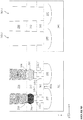
- FIG. 1 shows a simplified top-down schematic view of an integrated circuit 100 , in accordance with an embodiment.
- FIGS. 2A and 2B show embodiment diagrammatic cross-sectional views of the integrated circuit 100 of FIG. 1 along the line A-A (for example, in an x-z plane), in accordance with various embodiments.
- FIGS. 2C to 2E show various diagrammatic cross-sectional views of the integrated circuit 100 of FIG. 1 along the line B-B (for example, in the x-z plane), in accordance with various embodiments.
- FIGS. 1 and 2A to 2E have been simplified for the sake of clarity and to highlight various features of the integrated circuit 100 .
- Some of the features described below in reference to the examples of FIGS. 1 and 2A to 2E can be replaced, modified, or eliminated in other embodiments of the integrated circuit 100 .
- other features may be added to the embodiments of FIGS. 1 and 2A to 2E without departing from the scope of this disclosure.
- the integrated circuit 100 includes a substrate (e.g. a wafer) 101 .
- the substrate 101 may include silicon. Additionally or alternatively, the substrate 101 includes another elementary semiconductor material, such as germanium; a compound semiconductor material, such as silicon carbide, silicon phosphide, gallium arsenide, gallium phosphide, indium phosphide, indium arsenide, and/or indium antimonide; an alloy semiconductor material, such as SiGe, SiPC, GaAsP, AlInAs, AlGaAs, GaInAs, GaInP, and/or GaInAsP; or combinations thereof.
- the substrate 101 is a semiconductor-on-insulator substrate, such as a silicon-on-insulator (SOI) substrate, a silicon germanium-on-insulator (SGOI) substrate, or a germanium-on-insulator (GOI) substrate.
- semiconductor-on-insulator substrates can be fabricated using separation by implantation of oxygen (SIMOX), wafer bonding, and/or other suitable methods.
- substrate 101 includes one or more group III-V materials or one or more group II-IV materials.
- the substrate 101 includes various doped regions configured according to design requirements of the integrated circuit 100 .
- the substrate 101 may include p-type doped regions (for example, p-type wells) doped with p-type dopants, such as boron (for example, BF 2 ), indium, other p-type dopants, or combinations thereof.
- the substrate 101 may include n-type doped regions (for example, n-type wells) doped with n-type dopants, such as phosphorus, arsenic, other n-type dopants, or combinations thereof.
- the various doped regions can be formed directly on and/or in substrate 101 , for example, providing a p-well structure, an n-well structure, a dual-well structure, a raised structure, or combinations thereof. As described in further detail below, an ion implantation process, a diffusion process, or other suitable doping process can be performed either individually or in combination to form the various doped regions.
- the various doped regions of the substrate 101 are depicted as a p-well region 102 and an n-well region 104 that extend into the substrate 101 from a major surface 101 a of the substrate 101 .
- the p-well region 102 has a major surface 102 a that is substantially coplanar with the major surface 101 a of the substrate 101 .
- the n-well region 104 includes has a major surface 104 a that is substantially coplanar with the major surface 101 a of the substrate 101 .
- the major surfaces 101 a , 102 a , and 104 a may be planar surfaces that lie in an x-y plane of the integrated circuit 100 , as illustrated in the example of FIG. 2A .
- the p-well region 102 has a p-type dopant concentration of about 1 ⁇ 10 16 cm ⁇ 3 to about 1 ⁇ 10 19 cm ⁇ 3
- the n-well region 104 has an n-type dopant concentration of about 1 ⁇ 10 16 cm ⁇ 3 to about 1 ⁇ 10 19 cm ⁇ 3 .
- the p-well region 102 includes a circuit region (e.g. device region) 106 - 1 having one or more transistor structures formed therein.
- the p-well region 102 further includes a p-well pick-up region 108 - 1 having one or more p-well strap structures formed therein.
- the n-well region 104 includes a circuit region (e.g. device region) 106 - 2 having one or more transistor structures formed therein.
- the n-well region 104 further includes an n-well pick-up region 108 - 2 having one or more n-well strap structures.
- the p-well strap structures and n-well strap structures are described in further detail below in reference to FIGS. 2C to 2E .
- the one or more transistor structures in the circuit regions 106 - 1 , 106 - 2 may implement, or may be a part of, a memory cell or a circuit (e.g. a logic circuit).
- Examples of circuits that may be formed in the circuit regions 106 - 1 , 106 - 2 include, but are not limited to, inverters, NAND gates, NOR gates, AND gates, OR gates, flip-flops, among others.
- the transistor structure in the circuit region 106 - 1 of the p-well region 102 are depicted as two fins 110 - 1 , 110 - 2 .
- the transistor structure in the circuit region 106 - 2 of the n-well region 104 is depicted as two fins 118 - 1 , 118 - 2 .
- the transistor structure in the circuit regions 106 - 1 , 106 - 2 may have a different number of fins.
- embodiments of the present disclosure contemplate other types of transistor structures being formed in the circuit regions 106 - 1 , 106 - 2 (e.g., GAA transistors).
- fins 110 - 1 and 110 - 2 extend away from the substrate 101 from the major surface 102 a of the p-well region 102 and have the same conductivity-type as the p-well region 102
- fins 118 - 1 , 118 - 2 extend away from the substrate 101 from the major surface 104 a of the n-well region 104 and have the same conductivity-type as the n-well region 104 .
- the p-type dopant concentration of the fins 110 - 1 , 110 - 2 may be similar to the p-type dopant concentration of the p-well region 102
- the n-type dopant concentration of the fins 118 - 1 , 118 - 2 may be similar to the n-type dopant concentration of the n-well region 104 .
- the p-well region 102 , n-well region 104 , and fins 110 - 1 , 110 - 2 , 118 - 1 , 118 - 2 may be formed by any suitable process. In some embodiments, a combination of deposition, lithography, etching, and/or implantation processes are performed to define these features.
- an embodiment process for forming the p-well region 102 , n-well region 104 , and fins 110 - 1 , 110 - 2 , 118 - 1 , 118 - 2 includes forming fin structures from the substrate 101 and subsequently performing a doping process to define the p-well region 102 , n-well region 104 , and fins 110 - 1 , 110 - 2 , 118 - 1 , 118 - 2 .
- the step of forming fin structures from the substrate 101 includes performing a lithography process to form a patterned resist layer over the substrate 101 and performing an etching process to transfer a pattern defined in the patterned resist layer to the substrate 101 .
- the lithography process used to form the fin structures can include forming a resist layer on the substrate 101 (for example, by spin coating), performing a pre-exposure baking process, performing an exposure process using a mask, performing a post-exposure baking process, and performing a developing process.
- the resist layer is exposed to radiation energy (for example, ultraviolet (UV) light, deep UV (DUV) light, or extreme UV (EUV) light).
- UV ultraviolet
- DUV deep UV
- EUV extreme UV
- the mask blocks, transmits, and/or reflects radiation to the resist layer depending on a mask pattern of the mask and/or mask type (for example, binary mask, phase shift mask, or EUV mask), such that an image is projected onto the resist layer that corresponds with the mask pattern.
- the resist layer is sensitive to radiation energy, exposed portions of the resist layer chemically change, and exposed (or non-exposed) portions of the resist layer are dissolved during the developing process depending on characteristics of the resist layer and characteristics of a developing solution used in the developing process.
- the patterned resist layer includes a resist pattern that corresponds with the mask.
- the etching process that follows the lithography process uses the patterned resist layer as an etch mask to remove portions of the substrate 101 that are exposed.
- the etching process can include a dry etching process (for example, a reactive ion etching (RIE) process), a wet etching process, other suitable etching process, or combinations thereof.
- RIE reactive ion etching
- the patterned resist layer is removed from the substrate 101 , for example, by a resist stripping process, thereby defining fin structures extending out of the substrate 101 from the major surface 101 a of the substrate 101 .
- fin structures may be formed from the substrate 101 by a multiple patterning process, such as a double patterning lithography (DPL) process (for example, a lithography-etch-lithography-etch (LELE) process, a self-aligned double patterning (SADP) process, a spacer-is-dielectric (SID) SADP process, other double patterning process, or combinations thereof), a triple patterning process (for example, a lithography-etch-lithography-etch-lithography-etch (LELELE) process, a self-aligned triple patterning (SATP) process, other triple patterning process, or combinations thereof), other multiple patterning process (for example, self-aligned quadruple patterning (SAQP) process), or combinations thereof.
- DPL double patterning lithography
- LELE lithography-etch-lithography-etch
- SADP self-aligned double patterning
- SID spacer-is-dielectric
- a triple patterning process for example, a lithography-
- DSA directed self-assembly
- the exposure process can implement maskless lithography, electron-beam (e-beam) writing, ion-beam writing, and/or nanoimprint technology for patterning the resist layer and/or other layers.
- a doping process is performed.
- a lithography process is performed to mask (e.g. cover) a first region of the substrate 101 and fin structures formed in the first region, while a second region of the substrate 101 and fin structures formed in the second region are exposed.
- the second region of the substrate 101 and the fin structures formed therein are exposed to an ion implantation process and/or a diffusion process, thereby resulting in the p-well region 102 and fins 110 - 1 , 110 - 2 .
- a lithography process is then performed to cover the p-well region 102 and fins 110 - 1 , 110 - 2 , while the first region of the substrate 101 and the fin structures formed therein are exposed to an ion implantation process and/or a diffusion process, thereby resulting in the n-well region 104 and fins 118 - 1 , 118 - 2 .
- the sequence of steps used to form the p-well region 102 , n-well region 104 , and fins 110 - 1 , 110 - 2 , 118 - 1 , 118 - 2 may be different such that p-well region 102 and/or n-well region 104 are formed before forming fins 110 - 1 , 110 - 2 , 118 - 1 , 118 - 2 .
- the result is fins 110 - 1 , 110 - 2 that extend away from the substrate 101 from the major surface 102 a of the p-well region 102 , and fins 118 - 1 , 118 - 2 that extend away from the substrate 101 from the major surface 104 a of the n-well region 104 .
- the integrated circuit 100 includes various gate structures 112 - 1 , 112 - 2 .
- the gate structures 112 - 1 may be active gate structures disposed in the circuit regions 106 - 1 , 106 - 2 .
- An active gate structure generally refers to an electrically functional gate structure of a transistor device.
- gate structures 112 - 1 are formed over channel regions of fins 110 - 1 , 110 - 2 , 118 - 1 , 118 - 2 to enable current to flow between source and drain regions of fins 110 - 1 , 110 - 2 , 118 - 1 , 118 - 2 .
- the gate structures 112 - 2 may be dummy gate structures disposed in the circuit regions 106 - 1 , 106 - 2 and the well pick-up regions 108 - 1 , 108 - 2 .
- a dummy gate structure generally refers to an electrically non-functioning gate structure of a transistor device.
- the dummy gate structures 112 - 2 mimic physical properties of active gate structures 112 - 1 , such as physical dimensions of the active gate structures 112 - 1 , but are electrically inoperable and do not enable current to flow between source and drain regions of a transistor device.
- Each of the gate structures 112 - 1 , 112 - 2 may have a width W 1 (e.g. measured in the y direction in the top-down view of FIG. 1 ) that is substantially equal to a length of a channel formed between adjacent source/drain regions (e.g. in the range of about 2 nanometers and about 30 nanometers). It is also noted that the dummy gate structures 112 - 2 and the active gate structures 112 - 1 have the same routing direction (e.g. in the x-direction).
- Gate structures 112 - 1 , 112 - 2 may be formed using a gate-first process, a gate-last process, or a hybrid gate last/gate first process.
- the gate structures 112 - 1 , 112 - 2 may be implemented using gate stacks including a gate dielectric, a gate electrode, and a hard mask layer.
- the gate dielectric includes a dielectric material, such as silicon oxide, a high-k dielectric material, other suitable dielectric material, or combinations thereof.
- a high-k dielectric material generally refers to dielectric materials having a dielectric constant (k), for example, greater than that of silicon oxide (where k of silicon oxide is about 3.9).
- gate dielectric further includes an interfacial layer (including a dielectric material, such as silicon oxide) disposed between the high-k dielectric layer and fins 110 - 1 , 110 - 2 , 118 - 1 , 118 - 2 .
- Gate electrode is disposed over the gate dielectric.
- the gate electrode includes an electrically conductive material, and in some embodiments, the gate electrode includes multiple layers, such as a capping layer, a work function layer, a glue/barrier layer, and a metal fill (or bulk) layer.
- the capping layer includes a metal and nitrogen, such as titanium nitride (TiN), tantalum nitride (TaN), tungsten nitride (W2N), titanium silicon nitride (TiSiN), tantalum silicon nitride (TaSiN), or combinations thereof.
- the work function layer can include a conductive material tuned to have a desired work function (such as an n-type work function or a p-type work function), such as n-type work function materials and/or p-type work function materials.
- P-type work function materials include TiN, TaN, Ru, Mo, Al, WN, ZrSi 2 , MoSi 2 , TaSi 2 , NiSi 2 , WN, other p-type work function material, or combinations thereof.
- N-type work function materials include Ti, Al, Ag, Mn, Zr, TiAl, TiAlC, TaC, TaCN, TaSiN, TaAl, TaAlC, TiAlN, other n-type work function material, or combinations thereof.
- the glue/barrier layer can include a material that promotes adhesion between adjacent layers, such as the work function layer and the metal fill layer, and/or a material that blocks and/or reduces diffusion between gate layers, such as such as the work function layer and the metal fill layer.
- the glue/barrier layer includes metal (for example, W, Al, Ta, Ti, Ni, Cu, Co, other suitable metal, or combinations thereof), metal oxides, metal nitrides (for example, TiN), or combinations thereof.
- the metal fill layer can include a suitable conductive material, such as Al, W, and/or Cu.
- Gate dielectric and/or gate electrode may include numerous other layers, for example, capping layers, interface layers, diffusion layers, barrier layers, hard mask layers, or combinations thereof.
- the hard mask layer is disposed over the gate electrode and includes any suitable material, such as silicon and nitrogen (for example, silicon nitride).
- the gate structures 112 - 1 , 112 - 2 includes gate spacers 114 disposed adjacent to (for example, along sidewalls of) the respective gate structures 112 - 1 , 112 - 2 .
- Gate spacers 114 may be formed by any suitable process and may include one or more dielectric materials.
- the gate spacers 114 may include a single layer or multiple layers of materials, including SiO 2 , SiON, Si 3 N 4 , SiOCN, a dielectric material having a dielectric constant less than 3.5, or combinations thereof.
- FIG. 2A shows an isolation layer 202 (e.g. a non-conformal isolation layer) that is formed on the substrate 101 (e.g. on the major surface 101 a of the substrate 101 ) to separate and isolate circuit regions 106 - 1 , 106 - 2 , the p-well pick-up region 108 - 1 , and the n-well pick-up region 108 - 2 from one another.
- the isolation layer 202 further separates and isolates fins 110 - 1 , 110 - 2 , 118 - 1 , 118 - 2 from one another.
- FIG. 2A shows an isolation layer 202 (e.g. a non-conformal isolation layer) that is formed on the substrate 101 (e.g. on the major surface 101 a of the substrate 101 ) to separate and isolate circuit regions 106 - 1 , 106 - 2 , the p-well pick-up region 108 - 1 , and the n-well pick-up region 108 - 2 from one another
- the isolation layer 202 laterally surrounds a bottom portion BP of each of the fins 110 - 1 , 110 - 2 , 118 - 1 , 118 - 2 .
- the isolation layer 202 may include silicon oxide, silicon nitride, silicon oxynitride, other suitable isolation material (for example, including silicon, oxygen, nitrogen, carbon, or other suitable isolation constituent), or combinations thereof.
- the isolation layer 202 may include, or may be, a shallow trench isolation (STI) structure, deep trench isolation (DTI) structure, and/or local oxidation of silicon (LOCOS) structure.
- STI shallow trench isolation
- DTI deep trench isolation
- LOC local oxidation of silicon
- the isolation layer 202 may include a multi-layer structure that fills trenches, such as a bulk dielectric layer disposed over a liner dielectric layer, where the bulk dielectric layer and the liner dielectric layer include materials depending on design requirements (for example, a bulk dielectric layer that includes silicon nitride disposed over a liner dielectric layer that includes thermal oxide).
- the isolation layer 202 includes a dielectric layer disposed over a doped liner layer (including, for example, boron silicate glass (BSG) or phosphosilicate glass (PSG)).
- the isolation layer 202 can be formed by depositing (e.g. blanket depositing) an insulator material on substrate 101 after forming fins 110 - 1 , 110 - 2 , 118 - 1 , 118 - 2 , such that the insulator material layer fills gaps (e.g. trenches) between fins 110 - 1 , 110 - 2 , 118 - 1 , 118 - 2 , and etching back the insulator material layer to expose a top portion TP of the fins 110 - 1 , 110 - 2 , 118 - 1 , 118 - 2 , thereby forming the isolation layer 202 .
- gaps e.g. trenches
- a height of each of the fins 110 - 1 , 110 - 2 , 118 - 1 , 118 - 2 (e.g. as measured along the z-direction from the major surface 101 a of the substrate 101 to a farthest-most surface of the channel region fins 110 - 1 , 110 - 2 , 118 - 1 , 118 - 2 ) may be greater than 80 nanometers. It is also noted that in embodiments where transistor structures are implemented as GAA-type transistors, a distance (e.g. as measured along the z-direction) from the major surface 101 a of the substrate 101 to a farthest-most surface of the GAA channel region may also be greater than 80 nanometers.
- the circuit region 106 - 1 of the p-well region 102 may have one or more n-type metal-oxide-semiconductor (NMOS) transistors formed therein, while the circuit region 106 - 2 of the n-well region 104 may have one or more p-type MOS (PMOS) transistors formed therein.
- the NMOS transistors may include epitaxial source features and epitaxial drain features (referred to as epitaxial source/drain features 204 ) disposed over the source/drain regions of fins 110 - 1 , 110 - 2 .
- the PMOS transistors may include epitaxial source/drain features 206 disposed over the source/drain regions of fins 118 - 1 , 118 - 2 .
- semiconductor material may be epitaxially grown on fins 110 - 1 , 110 - 2 and 118 - 1 , 118 - 2 , forming epitaxial source/drain features 204 and 206 , respectively.
- epitaxial source/drain features 204 and 206 are respectively formed over the source/drain regions of fins 110 - 1 , 110 - 2 and 118 - 1 , 118 - 2 after a fin recess process (for example, an etch back process), such that epitaxial source/drain features 204 and 206 are grown from recessed fins 110 - 1 , 110 - 2 and 118 - 1 , 118 - 2 , respectively.
- the epitaxial source/drain features 204 and 206 may wrap the source/drain regions of fins 110 - 1 , 110 - 2 and 118 - 1 , 118 - 2 , respectively.
- fins 110 - 1 , 110 - 2 , 118 - 1 , 118 - 2 may not be subjected to a fin recess process.
- epitaxial source/drain features 204 , 206 extend (e.g. grow) laterally along the x-direction (in some embodiments substantially perpendicular to fins 110 - 1 , 110 - 2 , 118 - 1 , 118 - 2 ), such that epitaxial source/drain features 204 , 206 are merged features that span more than one fin.
- epitaxial source/drain feature 204 spans fins 110 - 1 , 110 - 2
- epitaxial source/drain feature 206 spans fins 118 - 1 , 118 - 2 .
- An epitaxy process can implement CVD deposition techniques (for example, vapor-phase epitaxy (VPE), ultra-high vacuum CVD (UHV-CVD), LPCVD, and/or PECVD), molecular beam epitaxy, other suitable SEG processes, or combinations thereof.
- CVD deposition techniques for example, vapor-phase epitaxy (VPE), ultra-high vacuum CVD (UHV-CVD), LPCVD, and/or PECVD
- molecular beam epitaxy other suitable SEG processes, or combinations thereof.
- the epitaxy process can use gaseous and/or liquid precursors.
- Epitaxial source/drain feature 204 is doped with n-type dopants, while epitaxial source/drain feature 206 is doped with p-type dopants. Consequently, epitaxial source/drain feature 204 may function as an n-doped source/drain region of the NMOS transistor in the circuit region 106 - 1 of the p-well region 102 , and epitaxial source/drain feature 206 may function as a p-doped source/drain region of the PMOS transistor in the circuit region 106 - 2 of the n-well region 104 .
- the epitaxial source/drain feature 204 includes epitaxial layers including silicon and/or carbon, where silicon-containing epitaxial layers or silicon-carbon-containing epitaxial layers are doped with phosphorous, arsenic, other n-type dopants, or combinations thereof (for example, forming a Si:P epitaxial layer, a Si:C epitaxial layer, a Si:C:P epitaxial layer, a Si:As epitaxial layer, or combinations thereof).
- Epitaxial source/drain feature 206 includes epitaxial layers including silicon and/or germanium, where the silicon germanium containing epitaxial layers are doped with boron, carbon, other p-type dopants, or combinations thereof (for example, forming a Si:Ge:B epitaxial layer or a Si:Ge:C epitaxial layer).
- the epitaxial source/drain feature 204 has an n-type dopant concentration of about 5 ⁇ 10 19 cm ⁇ 3 to about 1 ⁇ 10 22 cm ⁇ 3
- the epitaxial source/drain feature 206 has a p-type dopant concentration of about 1 ⁇ 10 19 cm ⁇ 3 to about 6 ⁇ 10 21 cm ⁇ 3 .
- the epitaxial source/drain features 204 , 206 may include materials and/or dopants that achieve desired tensile stress and/or compressive stress in the channel regions of the NMOS and PMOS transistors, respectively.
- the p-doped epitaxial source/drain feature 206 is adjacent to a SiGe channel region where the atomic concentration of Ge is in a range of about 5 percent and about 35 percent.
- the epitaxial source/drain features 204 , 206 may be doped during deposition by adding impurities to a source material of the epitaxy process.
- the epitaxial source/drain features 204 , 206 may, alternatively or additionally, be doped by an ion implantation process subsequent to a deposition process.
- An annealing process may be performed to activate dopants in epitaxial source/drain features 204 , 206 .
- Doping of the epitaxial source/drain features 204 , 206 may be performed in conjunction with photomasks (e.g. N+ photomask or P+ photomask).
- the N+ photomask used to form the epitaxial source/drain feature 204 over the p-well region 102 may cover both the circuit region 106 - 1 and the pick-up region 108 - 1 of the p-well region 102 .
- the P+ photomask used to form the epitaxial source/drain feature 206 over the n-well region 104 may cover both the circuit region 106 - 2 and the pick-up region 108 - 2 of the n-well region 104 .
- This allows for simplicity in forming the doping masks for the epitaxial source/drain features 204 , 206 since, as described in further detail below in reference to FIGS. 2C to 2E , no anti-type source/drain masking step is required for doping the well pick-up regions 108 - 1 , 108 - 2 .
- silicide layers 208 , 210 may be formed on or within epitaxial source/drain features 204 , 206 , respectively.
- silicide layers 208 , 210 are formed by depositing a metal layer over epitaxial source/drain features 204 , 206 .
- the metal layer includes any material suitable for promoting silicide formation, such as nickel, platinum, palladium, vanadium, titanium, cobalt, tantalum, ytterbium, zirconium, other suitable metal, or combinations thereof.
- Integrated circuit 100 is then heated (for example, subjected to an annealing process) to cause constituents of epitaxial source/drain features 204 , 206 (for example, silicon and/or germanium) to react with the metal.
- the silicide layers 208 , 210 thus include metal and a material of epitaxial source/drain features 204 , 206 , respectively.
- the silicide layers 208 , 210 include nickel silicide, titanium silicide, or cobalt silicide. Any un-reacted metal, such as remaining portions of the metal layer, is selectively removed by any suitable process, such as an etching process.
- the integrated circuit 100 further includes one or more dielectric layers 212 , 214 , 216 disposed on or over the isolation layer 202 .
- a first dielectric layer 212 e.g. inter-layer dielectric 0, abbreviated as ILD-0
- a second dielectric layer 214 e.g. ILD-1
- a third dielectric layer 216 e.g. ILD-2
- the one or more dielectric layers 212 , 214 , 216 include a dielectric material including, for example, silicon oxide, silicon nitride, silicon oxynitride, TEOS formed oxide, PSG, BPSG, low-k dielectric material, other suitable dielectric material, or combinations thereof.
- exemplary low-k dielectric materials include FSG, carbon doped silicon oxide, Black Diamond® (Applied Materials of Santa Clara, Calif.), Xerogel, Aerogel, amorphous fluorinated carbon, Parylene, BCB, SILK® (Dow Chemical, Midland, Mich.), polyimide, other low-k dielectric material, or combinations thereof.
- one or more dielectric layers 212 , 214 , 216 may include a low-k dielectric material (generally referred to as low-k dielectric layers, which may have a dielectric constant (k) that is less than 3).
- etch stop layers there may be one or more etch stop layers (ESLs) 223 , 225 , 227 formed in the integrated circuit 100 .
- ESLs etch stop layers
- the embodiment shown in FIG. 2B shows ESL 223 lining (e.g. conformally formed over) the sidewalls of the top portions TP of fins 110 - 1 , 110 - 2 , 118 - 1 , 118 - 2 and the sidewalls of the epitaxial source/drain features 204 , 206 .
- the ESL 223 is also disposed on the isolation layer 202 . Consequently, ESL 223 physically separates the isolation layer 202 from the dielectric layer 212 .
- ESL 225 formed between dielectric layer 212 and dielectric layer 214 .
- ESL 227 is formed between dielectric layer 214 and dielectric layer 216 .
- the ESLs 223 , 225 , 227 include a material different from the isolation layer 202 and/or dielectric layers 212 , 214 , 216 .
- ESLs 223 , 225 , 227 include silicon and nitrogen, such as silicon nitride or silicon oxynitride.
- the dielectric layers 212 , 214 , 216 and the ESLS 223 , 225 , 227 may be formed by a deposition process (e.g. blanket deposition process), such as CVD, PVD, ALD, HDPCVD, MOCVD, RPCVD, PECVD, LPCVD, ALCVD, APCVD, plating, other suitable methods, or combinations thereof.
- a deposition process e.g. blanket deposition process
- the dielectric layers 212 , 214 , 216 and the ESLS 223 , 225 , 227 are formed by a flowable CVD (FCVD) process that includes, for example, depositing a flowable material (such as a liquid compound) on an underlying layer and converting the flowable material to a solid material by a suitable technique, such as thermal annealing and/or ultraviolet radiation treating. Subsequent to the deposition of the dielectric layers 212 , 214 , 216 , a CMP process and/or other planarization process is performed, such that the dielectric layers 212 , 214 , 216 have substantially planar surfaces.
- FCVD flowable CVD
- Contacts 218 - 3 , 220 - 3 and vias 222 - 3 , 224 - 3 are disposed in the one or more dielectric layers 212 , 214 , 216 to form interconnect structures.
- the contacts 218 - 3 , 220 - 3 and vias 222 - 3 , 224 - 3 include any suitable electrically conductive material, such as Ta, Ti, Al, Ni, Mo, Pt, Ru, Cu, Co, W, TiN, TaN, other suitable conductive materials, or combinations thereof.
- contacts 218 - 3 , 220 - 3 and vias 222 - 3 , 224 - 3 can be combined to provide contacts 218 - 3 , 220 - 3 and vias 222 - 3 , 224 - 3 with various layers, such as a barrier layer, an adhesion layer, a liner layer, a bulk layer, other suitable layer, or combinations thereof.
- contacts 218 - 3 , 220 - 3 include Ti, TiN, and/or Co
- vias 222 - 3 , 224 - 3 include Ti, TiN.
- the contacts 218 - 3 , 220 - 3 and vias 222 - 3 , 224 - 3 are formed by patterning the one or more dielectric layers 212 , 214 , 216 .
- Patterning the one or more dielectric layers 212 , 214 , 216 can include lithography processes and/or etching processes to form openings (trenches), such as contact openings and/or via openings in respective dielectric layers 212 , 214 , 216 .
- the lithography processes include forming a resist layer over respective dielectric layers 212 , 214 , 216 , exposing the resist layer to patterned radiation, and developing the exposed resist layer, thereby forming a patterned resist layer that can be used as a masking element for etching opening(s) in respective dielectric layers 212 , 214 , 216 .
- the etching processes include dry etching processes, wet etching processes, other etching processes, or combinations thereof. Thereafter, the opening(s) are filled with one or more conductive materials.
- the conductive material(s) can be deposited by PVD, CVD, ALD, electroplating, electroless plating, other suitable deposition process, or combinations thereof.
- any excess conductive material(s) can be removed by a planarization process, such as a CMP process, thereby planarizing a top surface of dielectric layers 212 , 214 , 216 , contacts 218 - 3 , 220 - 3 and vias 222 - 3 , 224 - 3 .
- a planarization process such as a CMP process
- Contact 218 - 3 (also referred to as a local interconnect or local contact) electrically and/or physically couples a source/drain region, such as the epitaxial source/drain feature 204 , of the NMOS transistor in the p-well region 102 to via 222 - 3 .
- contact 220 - 3 electrically and/or physically couples a source/drain region, such as the epitaxial source/drain feature 206 , of the PMOS transistor in the n-well region 104 to via 222 - 4 .
- via 222 - 3 is disposed on contact 218 - 3 , such that via 222 - 3 electrically and/or physically couples contact 218 - 3 to a first power supply line M 1 - 1 , which may be electrically connected to a first power supply voltage VSS.
- FIG. 2A also shows that via 224 - 3 is disposed on contact 220 - 3 , such that via 224 - 3 electrically and/or physically couples contact 220 - 3 to a second power supply line M 1 - 2 , which may be electrically connected to a second power supply voltage VDD.
- the first power supply voltage VSS may be configured as ground and/or a negative supply voltage, depending on design requirements.
- the second power supply voltage VDD may be configured as a positive supply voltage, depending on design requirements.
- the p-well region 102 additionally includes the p-well pick-up region 108 - 1
- the n-well region 104 additionally includes the n-well pick-up region 108 - 2
- the p-well pick-up region 108 - 1 which may be devoid of transistor structures, includes a p-well strap structure that electrically and/or physically couples the p-well region 102 to the first power supply voltage VSS.
- the n-well pick-up region 108 - 2 which may also be free from transistor structures, includes an n-well strap structure that electrically and/or physically couples the n-well region 104 to the second power supply voltage VDD.
- FIG. 2C shows a first embodiment of a p-well strap structure 226 - 1 , 230 - 1 and an n-well strap structure 228 - 1 , 232 - 1 .
- the p-well strap structure 226 - 1 , 230 - 1 includes a first conductive plug 226 - 1 that extends through the second dielectric layer 214 , the first dielectric layer 212 , and the isolation layer 202 to physically contact the major surface 102 a of the p-well region 102 .
- the n-well strap structure 228 - 1 , 232 - 1 includes a second conductive plug 228 - 1 that extends through the second dielectric layer 214 , the first dielectric layer 212 , and the isolation layer 202 to physically contact the major surface 104 a of the n-well region 104 .
- the conductive plug 226 - 2 shown in FIG. 1 is similar in structure, size, and composition to the conductive plug 226 - 1
- the conductive plug 228 - 2 shown in FIG. 1 is similar in structure, size, and composition to the conductive plug 228 - 1 .
- Each of the conductive plugs 226 - 1 , 226 - 2 , 228 - 1 , 228 - 2 may have a first dimension (e.g. a width W 2 measured in the y direction in the top-down view of FIG. 1 ) that is between 5 nanometers and 60 nanometers, and a second dimension (e.g. a width W 3 measured in the x direction in the top-down view of FIG. 1 ) that is between 10 nanometers and 300 nanometers.
- a first dimension e.g. a width W 2 measured in the y direction in the top-down view of FIG. 1
- a second dimension e.g. a width W 3 measured in the x direction in the top-down view of FIG. 1
- the conductive plugs 226 - 1 , 226 - 2 , 228 - 1 , 228 - 2 may have a rectangular shape in a top-down view, and the width W 3 may be greater than the width W 2 by at least 1.5 times.
- the first conductive plug 226 - 1 and the second conductive plug 228 - 1 may include any suitable electrically conductive material, such as the materials described above in reference to contact 218 - 3 .
- the first conductive plug 226 - 1 and the second conductive plug 228 - 1 may include Ti, TiN, Ni, Mo, Pt, Co, Ru, W, TaN, Cu, or combinations thereof.
- the first conductive plug 226 - 1 and/or the second conductive plug 228 - 1 may include a single conductive material layer or may include a plurality of conductive material layers.
- the p-well strap structure 226 - 1 , 230 - 1 and n-well strap structure 228 - 1 , 232 - 1 also respectively include via 230 - 1 and via 232 - 1 that are formed in the third dielectric layer 216 .
- the via 230 - 1 is disposed on the first conductive plug 226 - 1 , such that via 230 - 1 electrically and/or physically couples first conductive plug 226 - 1 to power supply line 231 that may be electrically connected to the first power supply voltage VSS.
- the via 232 - 1 is disposed on the second conductive plug 228 - 1 , such that via 232 - 1 electrically and/or physically couples second conductive plug 228 - 1 to power supply line 233 that may be electrically connected to the second power supply voltage VDD.
- the vias 230 - 1 , 232 - 1 may include any suitable electrically conductive material, such as the materials described above in reference to via 222 - 3 .
- the first power supply voltage VSS may be provided to bias the p-well region 102
- the second power supply voltage VDD may be provided to bias the n-well region 104 .
- the proposed p-well strap structure 226 - 1 , 230 - 1 and n-well strap structure 228 - 1 , 232 - 1 provide several advantages, including reduced well pick-up resistance, significant improvements in latch-up performance, and efficient use of chip real estate. For example, since p-well strap structure 226 - 1 , 230 - 1 and n-well strap structure 228 - 1 , 232 - 1 physically contact the major surface of their respective well regions, contact area between conductive plugs and their respective well regions is increased, thereby reducing well pick-up resistance and improving latch-up immunity in integrated circuits (e.g. logic circuits or memory arrays) including the proposed well strap structures. Furthermore, as seen in FIG.
- FIG. 2D shows another embodiment of the n-well strap structure 226 - 1 , 230 - 1 and n-well strap structure 228 - 1 , 232 - 1 , where ESLs 223 , 225 , 227 are formed in the integrated circuit 100 .
- the first conductive plug 226 - 1 and the second conductive plug 228 - 1 extend through an entirety of the second dielectric layer 214 , the ESL 225 , the first dielectric layer 212 , the ESL 223 , and the isolation layer 202 to physically contact the major surface 102 a of the p-well region 102 and the major surface 104 a of the n-well region 104 , respectively.
- FIG. 2E shows another embodiment of the -well strap structure 226 - 1 , 230 - 1 and n-well strap structure 228 - 1 , 232 - 1 , where a silicide layers 234 , 236 is formed in p-well region 102 and n-well region 104 , respectively.
- the silicide layer 234 may include materials similar to the silicide layer 210
- silicide layer 236 may include materials similar to the silicide layer 208 .
- the embodiment shown in FIG. 2E provides the additional advantage of reducing pick-up RC effects in the well pick-up regions 108 - 1 , 108 - 2 .
- the silicide layers 234 , 236 may be formed using the processes described above in reference to silicide layers 208 , 210 .
- FIG. 3 shows a simplified schematic top-down view of an integrated circuit 300 , in accordance with an embodiment.
- the integrated circuit 300 includes the p-well region 102 , the n-well region 104 , the circuit regions 106 - 1 , 106 - 2 , and the well pick-up regions 108 - 1 , 108 - 2 described above in reference to FIGS. 1 and 2A to 2E .
- the cross-sectional views seen in FIGS. 2A and 2B may be the diagrammatic cross-sectional view of the integrated circuit 300 along the line C-C of FIG. 3 (for example, in the x-z plane), while FIGS. 2C to 2E may be diagrammatic cross-sectional views of the integrated circuit 300 along the line D-D of FIG. 3 .
- FIG. 3 also shows an additional circuit region 306 - 1 in the p-well region 102 and an additional circuit region 306 - 2 in the n-well region 104 .
- the additional circuit regions 306 - 1 , 306 - 2 may have one or more transistor structures formed therein.
- the one or more transistor structures in the additional circuit regions 306 - 1 , 306 - 2 may implement, or may be a part of, a memory cell or a circuit (e.g. a logic circuit).
- Examples of circuits that may be formed in the additional circuit regions 306 - 1 , 306 - 2 include, but are not limited to, inverters, NAND gates, NOR gates, AND gates, OR gates, flip-flops, among others.
- the integrated circuit 300 of FIG. 3 further includes dielectric gate structures 302 - 1 to 302 - 5 , which isolate (e.g. electrically isolate) the circuit regions 106 - 1 , 106 - 2 , the additional circuit regions 306 - 1 , 306 - 2 , and the well pick-up regions 108 - 1 , 108 - 2 from one another.
- the width of each of the dielectric gate structures 302 - 1 to 302 - 5 may be equal to the width W 1 described above in reference to FIG. 1 .
- the dielectric gate structures 302 - 1 to 302 - 5 and the active gate structures 112 - 1 have the same routing direction (e.g. in the x-direction shown in FIG. 3 ).
- the dielectric gate structures 302 - 1 to 302 - 5 may be closer to the major surface 101 a of the substrate 101 compared to the epitaxial source/drain features 204 , 206 .
- the dielectric gate structures 302 - 1 to 302 - 5 may extend deeper toward the substrate 101 than the epitaxial source/drain features 204 , 206 by at least 20 nanometers.
- the dielectric gate structures 302 - 1 to 302 - 5 may include a single layer or multiple layers of dielectric materials, including SiO 2 , SiOC, SiON, SiOCN, a carbon-containing oxide, a nitrogen-containing oxide, a carbon- and nitrogen-containing oxide, a metal oxide dielectric, HfO 2 , Ta 2 O 5 , TiO 2 , ZrO 2 , Al 2 O 3 , Y 2 O 3 , a metal-containing oxide, or combinations thereof.
- dielectric materials including SiO 2 , SiOC, SiON, SiOCN, a carbon-containing oxide, a nitrogen-containing oxide, a carbon- and nitrogen-containing oxide, a metal oxide dielectric, HfO 2 , Ta 2 O 5 , TiO 2 , ZrO 2 , Al 2 O 3 , Y 2 O 3 , a metal-containing oxide, or combinations thereof.
- the dielectric gate structure 302 - 2 serves to isolate the p-well pick-up region 108 - 1 from the circuit region 106 - 1
- the dielectric gate structure 302 - 4 serves to isolate the p-well pick-up region 108 - 1 from the additional circuit region 306 - 1
- the n-well pick-up region 108 - 2 is isolated from the circuit region 106 - 2 and the additional circuit region 306 - 2 by dielectric gate structures 302 - 2 and 302 - 4 , respectively.
- a well pick-up region can be separated from a circuit region by a single dummy gate (e.g. single dielectric gate structure 302 - 2 ) having a width substantially equal to a channel length (e.g. 2 nanometers to 30 nanometers). This obviates the need for a substantial dummy region/area between a circuit region and a well pick-up region, which, in turn, results in a more efficient use of chip area.
- a single dummy gate e.g. single dielectric gate structure 302 - 2
- a channel length e.g. 2 nanometers to 30 nanometers
- FIG. 4 shows a simplified schematic top-down view of an integrated circuit 400 , in accordance with an embodiment.
- the dielectric gate structure 302 - 3 between conductive plugs 226 - 1 and 226 - 2 is replaced with the metal dummy gate structure 112 - 2 since each of these conductive plugs 226 - 1 and 226 - 2 contact the same p-well region 102 and isolation between conductive plugs 226 - 1 and 226 - 2 may not be necessary.
- each of the conductive plugs 228 - 1 and 228 - 2 contact the same n-well region 104 , and thus, isolation between the conductive plugs 228 - 1 and 228 - 2 may not be necessary. It is noted that isolation between conductive plugs 226 - 1 , 226 - 2 and conductive plugs 228 - 1 , 228 - 2 by the isolation between the p-well region 102 and the n-well region 104 .
- FIG. 5 is a diagrammatic plan view showing a plurality of memory arrays 500 - 1 , 500 - 2 , each of which can implement well straps configured as described above, according to various aspects of the present disclosure.
- each memory array 500 - 1 , 500 - 2 is a static random access memory (SRAM) array.
- memory arrays 500 - 1 , 500 - 2 are another type of memory, such as a dynamic random access memory (DRAM), a non-volatile random access memory (NVRAM), a flash memory, or other suitable memory.
- DRAM dynamic random access memory
- NVRAM non-volatile random access memory
- Memory arrays 500 - 1 , 500 - 2 may be included in a microprocessor, a memory, and/or other IC device.
- memory arrays 500 - 1 , 500 - 2 may be a portion of an IC chip, an SoC, or portion thereof, that includes various passive and active microelectronic devices such as resistors, capacitors, inductors, diodes, PFETs, NFETs, MOSFETs, CMOS transistors, BJTs, LDMOS transistors, high voltage transistors, high frequency transistors, other suitable components, or combinations thereof.
- FIG. 5 has been simplified for the sake of clarity to better understand the inventive concepts of the present disclosure. Additional features can be added in memory arrays 500 - 1 , 500 - 2 , and some of the features described below can be replaced, modified, or eliminated in other embodiments of memory arrays 500 - 1 , 500 - 2 .
- Each of memory arrays 500 - 1 , 500 - 2 includes memory cells 501 , such as SRAM memory cells, configured to store data.
- memory cells 501 include various p-type FinFETs and/or n-type FinFETs.
- Memory cells 501 are arranged in column 1 to column N extending along a first direction (here, in a y-direction) and row 1 to row M extending along a second direction (here, in an x-direction), where N and M are positive integers.
- Column 1 to column N each include a bit line pair extending along the first direction, such as a bit line (BL) and a bit line bar (BLB) (also referred to as a complementary bit line), that facilitate reading data from and/or writing data to respective memory cells 501 in true form and complementary form on a column-by-column basis.
- Row 1 to row M each includes a word line (WL) (not shown) that facilitates access to respective memory cells 501 on a row-by-row basis.
- Each memory cell 501 is electrically connected to a respective BL, a respective BLB, and a respective WL, which are electrically connected to a controller 503 .
- Controller 503 is configured to generate one or more signals to select at least one WL and at least one-bit line pair (here, BL and BLB) to access at least one of memory cells 501 for read operations and/or write operations.
- Controller 503 includes any circuitry suitable to facilitate read/write operations from/to memory cells 501 , including but not limited to, a column decoder circuit, a row decoder circuit, a column selection circuit, a row selection circuit, a read/write circuit (for example, configured to read data from and/or write data to memory cells 501 corresponding to a selected bit line pair, in other words, a selected column), other suitable circuit, or combinations thereof.
- the controller 503 includes at least one sense amplifier configured to detect and/or amplify a voltage differential of a selected bit line pair. In some embodiments, the sense amplifier is configured to latch or otherwise store data values of the voltage differential.
- a perimeter of each of memory arrays 500 - 1 , 500 - 2 is configured with dummy cells, such as edge dummy cells and well strap cells, to ensure uniformity in performance of memory cells 501 .
- Dummy cells are configured physically and/or structurally similar to memory cells 501 , but do not store data.
- dummy cells can include p-type wells, n-type wells, fin structures (including one or more fins), gate structures, source/drain features, and/or contact features.
- Well strap cells generally refer to dummy cells that are configured to electrically couple a voltage to an n-type well of memory cells 501 , a p-type well of memory cells 501 , or both.
- row 1 to row M each begin with an edge dummy cell 505 a and end with an edge dummy cell 505 b , such that row 1 to row M of memory cells 501 are disposed between edge dummy cells 505 a and edge dummy cells 505 b .
- Edge dummy cells 505 a and edge dummy cells 505 b are arranged in respective columns extending along the first direction (here, the y-direction).
- the column of edge dummy cells 505 a and/or the column of edge dummy cells 505 b are substantially parallel to at least one bit line pair (here, BL and BLB) of memory array 500 .
- edge dummy cells 505 a and/or edge dummy cells 505 b are configured to connect respective memory cells 501 to respective WLs.
- edge dummy cells 505 a and/or edge dummy cells 505 b include circuitry for driving WLs.
- edge dummy cells 505 a and/or edge dummy cells 505 b are electrically connected to a second power supply voltage VDD (for example, a positive power supply voltage) and/or a first power supply voltage VSS (for example, an electrical ground) depending on design requirements of memory arrays 500 - 1 , 500 - 2 .
- VDD for example, a positive power supply voltage
- VSS for example, an electrical ground
- column 1 to column N each begin with a well strap cell 507 a and end with a well strap cell 507 b , such that column 1 to column N of memory cells 501 are disposed between well strap cells 507 a and well strap cells 507 b .
- Well strap cells 507 a and well strap cells 507 b are arranged in respective rows extending along the second direction (here, the x-direction).
- the row of well strap cells 507 a and the row of well strap cells 507 b are substantially parallel to at least one WL of memory arrays 500 - 1 , 500 - 2 .
- Well strap cells 507 a are disposed between one of edge dummy cells 505 a and one of edge dummy cells 505 b
- well strap cells 507 b are disposed between one of edge dummy cells 505 a and one of edge dummy cells 505 b
- well strap cells 507 a and/or well strap cells 507 b include an n-type well strap, a p-type well strap, or both an n-type well strap and a p-type well strap.
- well strap cells 507 a and/or well strap cells 507 b include an n-type well strap region having one or more n-type well straps disposed adjacent to a p-type well strap region having one or more p-type well straps.
- the n-type well strap region and the p-type well strap region may be disposed between dummy regions of the well strap cells 507 a and/or the well strap cells 507 b .
- the p-type well strap is configured as the p-well pick-up region 108 - 1 described above in reference to FIGS. 1, 2A to 2E, 3, and 4
- the n-type well strap is configured as the n-well pick-up region 108 - 2 described above in reference to FIGS. 1, 2A to 2E, 3, and 4 .
- FIG. 6 is a diagrammatic plan view showing a plurality of memory arrays 600 - 1 , 600 - 2 , each of which can implement well straps configured as described above, according to various aspects of the present disclosure. Similar features in FIGS. 5 and 6 are identified by the same reference numerals for clarity and simplicity.
- memory cells 501 along a given column of each memory array 500 - 1 , 500 - 2 share a common bit line BL and bit line bar BLB and a common controller 503 .
- the memory cells 501 of memory array 600 - 1 and the memory cells 501 of memory array 600 - 2 are coupled to different controllers.
- memory cells 501 of memory array 600 - 2 are coupled to controller 603 (which may be functionally and structurally similar to controller 503 ) by their respective bit lines BL and bit line bars BLB.
- FIGS. 7A to 7F show a process flow that may be used to form the p-well strap structure 226 - 1 , 230 - 1 and n-well strap structure 228 - 1 , 232 - 1 described above, in accordance with an embodiment.
- FIG. 7A shows a structure where fins 110 - 1 , 110 - 2 are formed in the circuit region 106 - 1 of the p-well region 102 , while fins 118 - 1 , 118 - 2 are formed in the circuit region 106 - 2 of the n-well region 104 using the process described in the foregoing description. It is noted that the no fin structures are formed in the well pick-up regions 108 - 1 , 108 - 2 .
- epitaxial source/drain features 204 , 206 are formed over the source/drain regions of fins 110 - 1 , 110 - 2 , 118 - 1 , 118 - 2 using the process described in the foregoing description. Additionally, silicide layers 208 , 210 are formed on or within the epitaxial source/drain features 204 , 206 using the process described in the foregoing description.
- the second dielectric layer 214 is subsequently deposited over the circuit regions 106 - 1 , 106 - 2 and well pick-up regions 108 - 1 , 108 - 2 to form the structure shown in FIG. 7A .
- openings 702 - 1 , 702 - 2 are formed in at least a portion of the second dielectric layer 214 in well pick-up regions 108 - 1 , 108 - 2 .
- the openings 702 - 1 , 702 - 2 expose portions of the top surface of the first dielectric layer 212 .
- the process used to form openings 702 - 1 , 702 - 2 is described above in reference to forming contacts 218 - 3 , 220 - 3 and vias 222 - 3 , 224 - 3 .
- a suitable patterning e.g.
- openings 704 - 1 , 704 - 2 are formed in the circuit regions 106 - 1 , 106 - 2 such that at least a portion of a major surface of each of the epitaxial source/drain features 204 , 206 is exposed.
- the openings 704 - 1 , 704 - 2 may expose at least a portion of the silicide layers 208 , 210 formed on or within the epitaxial source/drain features 204 , 206 .
- the etching process also extends the openings 702 - 1 , 702 - 2 into an entire thickness of each of the first dielectric layer 212 and the isolation layer 202 to expose at least a portion of the major surface 102 a of the p-well region 102 and at least a portion of the major surface 104 a of the n-well region 104 in the well pick-up regions 108 - 1 , 108 - 2 .
- Suitable patterning and etching processes include those described above in reference to forming contacts 218 - 3 , 220 - 3 and vias 222 - 3 , 224 - 3 .
- a conductive material (e.g. as described above in reference to contacts 218 - 3 , 220 - 3 ) is deposited into openings 704 - 1 , 704 - 2 to form contacts 218 - 3 , 220 - 3 .
- Suitable deposition processes have been described in reference to forming contacts 218 - 3 , 220 - 3 and vias 222 - 3 , 224 - 3 .
- the deposition process may also partially fill opening 702 - 1 with conductive material 706 - 1 and partially fill opening 702 - 2 with conductive material 706 - 2 .
- the conductive material 706 - 1 and 706 - 2 may subsequently form bottom portions of the first conductive plug 226 - 1 and the second conductive plug 228 - 1 , respectively.
- a silicidation process is performed after forming openings 702 - 1 , 702 - 2 but prior to the deposition of conductive material 706 - 1 , 706 - 2 .
- Such embodiments may be used when silicide layers 234 , 236 are desired in the p-well region 102 and the n-well region 104 .
- the silicide layers 234 , 236 may be formed using the processes described above in reference to silicide layers 208 , 210 .
- deposition of conductive material into the openings 702 - 1 , 702 - 2 continues to form the first conductive plug 226 - 1 and the second conductive plug 228 - 1 .
- a planarization process e.g. a CMP process
- a planarization process e.g. a CMP process
- the third dielectric layer 216 is formed over the second dielectric layer 214 , and vias 222 - 3 and 224 - 3 are formed in the third dielectric layer 216 using the process(es) described in the foregoing description.
- the process used for forming vias 230 - 1 , 232 - 1 in the well pick-up regions 108 - 1 , 108 - 2 may be similar to the process used for forming vias 222 - 3 and 224 - 3 in the circuit regions 106 - 1 , 106 - 2 .
- FIG. 8 shows a flow chart illustrating an embodiment method 800 of forming the p-well strap structure 226 - 1 , 230 - 1 and n-well strap structure 228 - 1 , 232 - 1 described above.
- the method 800 may, as an example, correspond to the process flow shown in FIGS. 7A to 7F .
- Method 800 includes step 802 of forming a first opening in a portion of an insulating layer, where the first opening is disposed over a well region having a first conductivity type and corresponding to a transistor having a second conductivity type.
- Step 802 may, as an example, correspond to the steps shown in FIGS. 7A and 7B .
- Method 800 also includes step 804 of forming a second opening in a portion of the insulating layer to expose a major surface of a source/drain structure of the transistor.
- Step 804 may, as an example, correspond to the step shown in FIG. 7C .
- Method 800 further includes step 806 of extending the first opening through an entire thickness of the insulating layer to expose a major surface of the well region.
- Step 806 may, as an example correspond to the step shown in FIG. 7C .
- Method 800 further includes step 808 of depositing a first conductive material in the first opening and a second conductive material in the second opening, where the first conductive material partially fills the first opening and the second conductive material fills the second opening.
- Step 808 may, as an example, correspond to the step shown in FIG.
- Method 800 additionally includes step 810 of depositing the first conductive material to fill the first opening and to form a conductive plug that extends through the entire thickness of the insulating layer to physically contact the major surface of the well region.
- Step 808 may, as an example, correspond to the step shown in FIG. 7E .
- FIGS. 7A to 7F illustrates an embodiment where a portion (e.g. bottom portion) of each conductive plug 226 - 1 , 228 - 1 is formed substantially contemporaneously with the contacts 218 - 3 , 220 - 3 .
- the conductive plugs 226 - 1 , 228 - 1 for the p-well strap structure 226 - 1 , 230 - 1 and n-well strap structure 228 - 1 , 232 - 1 may be formed separately from (e.g. before or after the formation of) the contacts 218 - 3 , 220 - 3 .
- FIGS. 9A to 9F show a process flow that may be used to form the p-well strap structure 226 - 1 , 230 - 1 and n-well strap structure 228 - 1 , 232 - 1 , where the contacts 218 - 3 , 220 - 3 are formed before forming the conductive plugs 226 - 1 , 228 - 1 .
- the contacts 218 - 3 , 220 - 3 are formed, e.g. using the processed described above, while the well pick-up regions 108 - 1 , 108 - 2 are masked and covered.
- FIGS. 9A to 9F show a process flow that may be used to form the p-well strap structure 226 - 1 , 230 - 1 and n-well strap structure 228 - 1 , 232 - 1 , where the contacts 218 - 3 , 220 - 3 are formed before forming the conductive plugs 226 - 1 , 228 - 1 .
- the conductive plugs 226 - 1 , 228 - 1 are formed, e.g. using the processed described above, while the circuit regions 106 - 1 , 106 - 2 are masked and covered. Subsequently, the mask that is covering the circuit regions 106 - 1 , 106 - 2 is removed to form the vias 222 - 3 , 224 - 3 in the circuit regions 106 - 1 , 106 - 2 and the vias 230 - 1 , 232 - 1 in the well pick-up regions 108 - 1 , 108 - 2 .
- FIG. 10 shows a flow chart illustrating an embodiment method 1000 of forming the p-well strap structure 226 - 1 , 230 - 1 and n-well strap structure 228 - 1 , 232 - 1 described above.
- the method 1000 may, as an example, correspond to the process flow shown in FIGS. 9A to 9F .
- Method 1000 includes step 1002 of forming a first opening in an insulating layer, where the first opening exposes a surface of a source/drain structure having a first conductivity type.
- Step 1002 may, as an example, correspond to the steps shown in FIGS. 9A and 9B .
- Method 1000 also includes step 1004 of depositing a first conductive material in the first opening to fill the first opening and form a contact that contacts the source/drain structure.
- Step 1004 may, as an example, correspond to the step shown in FIG. 9C .
- Method 1000 further includes step 1006 of masking the contact and step 1008 of forming a second opening extending through an entire thickness of the insulating layer to expose a major surface of a well region corresponding to the source/drain structure and having a second conductivity type different from the first conductivity type.
- Steps 1006 and 1008 may, as an example, correspond to the steps shown in FIG. 9D .
- Method 1000 additionally includes step 1010 of depositing a second conductive material in the second opening to fill the second opening and form a conductive plug that physically contacts the major surface of the well region.
- Step 1010 may, as an example, correspond to the step shown in FIG. 9E .
- first conductive plug 226 - 1 and the second conductive plug 228 - 1 are depicted as being continuous plugs having sidewalls that extend linearly or continuously from a top surface of a respective plug to a bottom surface of the respective plug.
- first conductive plug 226 - 1 or the second conductive plug 228 - 1 includes sidewalls having a stepped-like structure.
- FIG. 11 shows the first conductive plug 226 - 1 having a plurality of segments 1100 - 1 to 1100 - 4 . Adjacent segments are offset from each other in a lateral direction (e.g. the x-direction).
- the sidewalls of the first conductive plug 226 - 1 no longer extend linearly or continuously from a top surface thereof to a bottom surface thereof. Rather, the offset segments cause the sidewalls of the first conductive plug 226 - 1 to have a stepped-like structure.
- the first conductive plug 226 - 1 makes physical contact with the major surface 102 a of the well region 102 without the use of an intervening semiconductor structure (e.g. a fin) that extends from the major surface 102 a of the well region 102 , thereby providing the embodiment of FIG. 11 similar advantages as those discussed above in reference to other embodiments.
- the present disclosure proposes well straps that have reduced well pick-up resistance, that achieve significant improvements in latch-up performance, and that efficiently use chip real estate.
- this disclosure proposes using a conductive plug (e.g. a metal plug) that continuously extends through an inter-layer dielectric (ILD) layer and a shallow trench isolation (STI) layer to physically contact a major surface of well region so that contact area is increased, well pick-up resistance is reduced, and latch-up immunity is improved (e.g. in a logic circuit or a memory array including the proposed well strap).
- ILD inter-layer dielectric
- STI shallow trench isolation
- a silicide layer is formed in the well region and the conductive plug directly and physically contacts the silicide layer formed in the well region. Additionally, since contact between the conductive plug and the well region is made without the use of an intervening semiconductor structure (e.g. a fin) that extends from the major surface of the well region, no anti-type source/drain masking step is required for doping a well pick-up region. Furthermore, since contact between the conductive plug and the well region is made without the use of an intervening semiconductor structure (e.g. a fin) that extends from the major surface of the well region, a well pick-up region can be separated from a circuit region by a single dummy gate (e.g.
- the proposed well strap may be used in conjunction with fin-based logic circuit or memory cells or GAA-based logic circuits or memory cells. Furthermore, the proposed well strap does not affect desired characteristics of non-planar transistors used in the memory cells (e.g. voltage threshold in a FinFET used in a memory cells). Different embodiments may have different advantages, and no particular advantage is necessarily required of any embodiment.
- An embodiment integrated circuit structure includes a well region having a first conductivity type; a semiconductor structure, having the first conductivity type, extending away from the well region from a major surface of the well region; and a source/drain feature, having a second conductivity type different from the first conductivity type, disposed on the semiconductor structure.
- the embodiment integrated circuit structure further includes an isolation layer laterally surrounding at least a portion of the semiconductor structure; a dielectric layer disposed on the isolation layer, wherein at least a portion of the source/drain feature is disposed in the dielectric layer; and a conductive plug continuously extending through the dielectric layer and the isolation layer to physically contact the major surface of the well region, wherein the conductive plug is coupled to a power supply line to bias the well region.
- An embodiment integrated circuit structure includes a substrate; a p-type well region formed in the substrate; an n-type well region formed in the substrate; an isolation layer disposed on the substrate; and a dielectric layer disposed on the isolation layer.
- the p-type well region includes: a p-type semiconductor structure extending from a major surface of the p-type well region; an n-type source/drain region disposed on the p-type semiconductor structure; and a first contact disposed on a surface of the n-type source/drain region directed away from the major surface of the p-type well region.
- the n-type well region includes: an n-type semiconductor structure extending from a major surface of the n-type well region; a p-type source/drain region disposed on the n-type semiconductor structure; and a second contact disposed on a surface of the p-type source/drain region directed away from the major surface of the n-type well region. At least a portion of the p-type semiconductor structure and at least a portion of the n-type semiconductor structure are disposed in the isolation layer, and at least a portion of the n-type source/drain region and at least a portion of the p-type source/drain region are disposed in the dielectric layer.
- the embodiment integrated circuit structure further includes: a first plug element extending through an entire thickness of each of the dielectric layer and the isolation layer to physically contact the major surface of the p-type well region; and a second plug element extending through the entire thickness of each of the dielectric layer and the isolation layer to physically contact the major surface of the n-type well region.
- An embodiment method includes: forming a first opening in a first portion of an insulating layer, wherein the first opening is disposed over a well region having a first conductivity type, the well region corresponding to a transistor having a second conductivity type; forming a second opening in a second portion of the insulating layer to expose a major surface of a source/drain structure of the transistor, the source/drain structure being disposed on a fin having the first conductivity type, the fin extending away from the well region from a major surface of the well region; extending the first opening through an entire thickness of the insulating layer to expose at least a portion of the major surface of the well region; and depositing a first conductive material in the first opening to form a conductive plug that extends through the entire thickness of the insulating layer and physically contacts the major surface of the well region.
Landscapes
- Engineering & Computer Science (AREA)
- Microelectronics & Electronic Packaging (AREA)
- General Engineering & Computer Science (AREA)
- Computer Hardware Design (AREA)
- Metal-Oxide And Bipolar Metal-Oxide Semiconductor Integrated Circuits (AREA)
Abstract
Description
- This application is a Continuation of U.S. patent application Ser. No. 16/433,540, filed Jun. 6, 2019, which further claims priority to U.S. Provisional Patent Application Ser. No. 62/724,471 filed Aug. 29, 2018. The entire disclosures of which are herein incorporated by reference.
- The semiconductor integrated circuit (IC) industry has experienced exponential growth. Technological advances in IC materials and design have produced generations of ICs where each generation has smaller and more complex circuits than the previous generation. In the course of IC evolution, functional density (i.e., the number of interconnected devices per chip area) has generally increased while geometry size (i.e., the smallest component, or line, that can be created using a fabrication process) has decreased.
- This scaling down process generally provides benefits by increasing production efficiency and lowering associated costs. However, the scaling down process has also increased the complexity of processing and manufacturing ICs. For example, the scaling down process has led to increased pick-up resistance and reduced latch-up performance (e.g. degraded latch-up immunity) in well strap cells. Accordingly, although existing well strap cells have been generally adequate for their intended purposes, they have not been entirely satisfactory in all respects. Further improvements in well strap cells may be needed.
- The present disclosure is best understood from the following detailed description when read with the accompanying figures. It is emphasized that, in accordance with the standard practice in the industry, various features are not drawn to scale and are used for illustration purposes only. In fact, the dimensions of the various features may be arbitrarily increased or reduced for clarity of discussion.
-
FIGS. 1, 3, and 4 show simplified top-down schematic views of integrated circuits, in accordance with various embodiments. -
FIGS. 2A to 2E show simplified cross-sectional views of the schematic top-down views shown inFIGS. 1, 3, and 4 , in accordance with various embodiments. -
FIGS. 5 and 6 show simplified top-down schematic views of memory arrays, which can implement well strap structures configured as described herein, in accordance with various embodiments. -
FIGS. 7A to 7F andFIGS. 9A to 9F show process flows for forming well strap structures configured as described herein, in accordance with various embodiments. -
FIGS. 8 and 10 show flow charts describing methods for forming well strap structures configured as described herein, in accordance with various embodiments; -
FIG. 11 shows simplified cross-sectional view of well strap structures, in accordance with another embodiment. - The following disclosure provides many different embodiments, or examples, for implementing different features of the provided subject matter. Specific examples of components and arrangements are described below to simplify the present disclosure. These are, of course, merely examples and are not intended to be limiting. For example, the formation of a first feature over or on a second feature in the description that follows may include embodiments in which the first and second features are formed in direct contact and may also include embodiments in which additional features may be formed between the first and second features, such that the first and second features may not be in direct contact. In addition, the present disclosure may repeat reference numerals and/or letters in the various examples. This repetition is for the purpose of simplicity and clarity and does not in itself dictate a relationship between the various embodiments and/or configurations discussed.
- Further, spatially relative terms, such as “beneath,” “below,” “lower,” “above,” “upper” and the like, may be used herein for ease of description to describe one element or feature's relationship to another element(s) or feature(s) as illustrated in the figures. The spatially relative terms are intended to encompass different orientations of the device in use or operation in addition to the orientation depicted in the figures. The apparatus may be otherwise oriented (rotated 90 degrees or at other orientations) and the spatially relative descriptors used herein may likewise be interpreted accordingly. Still further, when a number or a range of numbers is described with “about,” “approximate,” and the like, the term is intended to encompass numbers that are within +/−10% of the number described, unless otherwise specified. For example, the term “about 5 nm” encompasses the dimension range from 4.5 nm to 5.5 nm.
- For advanced IC technology nodes, non-planar transistors (e.g. fin-like field effect transistors (FinFETs) or gate-all-around-like (GAA) FETs) have become a popular and promising candidate for high performance and low leakage applications. Logic circuits and memory arrays (such as static random access memory (SRAM) arrays) often incorporate non-planar transistors to enhance performance. The performance of logic circuits and memory cells is largely layout dependent. For example, it has been observed that an inner memory cell of a memory array performs differently than an edge memory cell of the memory array. In some layouts, inner memory cells and edge memory cells exhibit different threshold voltages (Vt), different on-currents (Ion), and/or different off-currents (Ioff).
- A well strap (also referred to as an electrical tie) electrically connects a well region corresponding with a transistor (e.g. of a logic circuit or a memory cell) to a voltage node (or voltage line). For example, a fin-based n-type well strap electrically connects an n-well region corresponding with a p-type FinFET to a voltage node, such as a voltage node associated with the p-type transistor, while a fin-based p-type well strap electrically connects a p-well region corresponding with an n-type FinFET to a voltage node, such as a voltage node associated with the n-type transistor. Well straps have thus been implemented to stabilize well potential and facilitate uniform charge distribution throughout a logic circuit or a memory array, thereby allowing for uniform performance among components of a logic circuit or among memory cells of the memory array.
- However, as smaller technology nodes (for example, 20 nm, 16 nm, 10 nm, 7 nm, and below) are introduced, decreasing the dimension and pitch of non-planar transistors in a well strap has diminished benefits provided by such transistors and well straps. For example, in a fin-based well strap, decreasing fin widths has been observed to increase well pick-up resistance, such that well pick-up resistance of a fin-based well strap is higher than the well pick-up resistance of a planar-based well strap. Such increases in well pick-up resistance degrades latch-up performance (e.g. degrades latch-up immunity) of memory arrays using fin-based well straps. It is noted that the degradation in latch-up performance and the increase in well pick-up resistance is also observed in well straps based on other non-planar-type transistors (e.g. GAA transistors).
- In addition to degraded latch-up performance and increased well pick-up resistance, typical well straps may include a source/drain structure that has a conductivity-type that is opposite to the source/drain structure of its corresponding transistor. For example, an n-type well strap may include an n-type semiconductor structure to electrically connect an n-well region corresponding with a p-doped source/drain structure of a p-type FinFET to a voltage node, while a p-type well strap may include a p-type semiconductor structure to electrically connect a p-well region corresponding with an n-doped source/drain structure of an n-type FinFET to a voltage node. This difference in the conductivity-type of the source/drain structures of a transistor and the semiconductor structure of its corresponding well strap requires anti-type source/drain doping to appropriately dope the source/drain structure of a transistor and the semiconductor structure of its corresponding well strap. This anti-type source/drain doping negatively impacts the size of a well pick-up region and increases the complexity of a lithography/patterning step for n+ doping of the source/drain structures of an n-type transistor and p+ doping of the source/drain structures of a p-type transistor.
- In view of the challenges described above, the present disclosure proposes well straps that have reduced well pick-up resistance, achieve significant improvements in latch-up performance, and efficiently use chip real estate. For example, this disclosure proposes using a conductive plug (e.g. a metal plug) that extends fully through an isolation layer (e.g. shallow trench isolation layer) to physically contact a major surface of a well region so that well pick-up resistance is reduced and latch-up immunity is improved (e.g., in a logic circuit or a memory array including the proposed well strap). Contact between the conductive plug and the well region is made without the use of an intervening semiconductor structure (e.g. a fin) that extends from the major surface of the well region. In some embodiments, a silicide layer is formed in the well region and the conductive plug physically contacts the silicide layer formed in the well region. Additionally, since contact between the conductive plug and the well region is made without the use of an intervening semiconductor structure that extends from the major surface of the well region, no anti-type source/drain masking step is required for doping a well pick-up region. Furthermore, since contact between the conductive plug and the well region is made without the use of an intervening semiconductor structure that extends from the major surface of the well region, a well pick-up region can be separated from a circuit region by a single dummy gate (e.g. dielectric dummy gate) having a width substantially equal to a channel length (e.g. 2 nanometers to 30 nanometers). This obviates the need for a substantial dummy region/area between a circuit region and a well pick-up region, which, in turn, results in a more efficient use of chip area. The proposed well strap may be used in conjunction with fin-based logic circuit or memory cells or GAA-based logic circuits or memory cells. Furthermore, the proposed well strap does not affect desired characteristics of non-planar transistors used in memory cells (e.g. voltage threshold in a FinFET used in a memory cells). Different embodiments may have different advantages, and no particular advantage is necessarily required of any embodiment.
-
FIG. 1 shows a simplified top-down schematic view of anintegrated circuit 100, in accordance with an embodiment.FIGS. 2A and 2B show embodiment diagrammatic cross-sectional views of theintegrated circuit 100 ofFIG. 1 along the line A-A (for example, in an x-z plane), in accordance with various embodiments.FIGS. 2C to 2E show various diagrammatic cross-sectional views of theintegrated circuit 100 ofFIG. 1 along the line B-B (for example, in the x-z plane), in accordance with various embodiments. It is noted thatFIGS. 1 and 2A to 2E have been simplified for the sake of clarity and to highlight various features of theintegrated circuit 100. Some of the features described below in reference to the examples ofFIGS. 1 and 2A to 2E can be replaced, modified, or eliminated in other embodiments of theintegrated circuit 100. Furthermore, other features may be added to the embodiments ofFIGS. 1 and 2A to 2E without departing from the scope of this disclosure. - Referring to
FIGS. 1 and 2A , theintegrated circuit 100 includes a substrate (e.g. a wafer) 101. Thesubstrate 101 may include silicon. Additionally or alternatively, thesubstrate 101 includes another elementary semiconductor material, such as germanium; a compound semiconductor material, such as silicon carbide, silicon phosphide, gallium arsenide, gallium phosphide, indium phosphide, indium arsenide, and/or indium antimonide; an alloy semiconductor material, such as SiGe, SiPC, GaAsP, AlInAs, AlGaAs, GaInAs, GaInP, and/or GaInAsP; or combinations thereof. In some embodiments, thesubstrate 101 is a semiconductor-on-insulator substrate, such as a silicon-on-insulator (SOI) substrate, a silicon germanium-on-insulator (SGOI) substrate, or a germanium-on-insulator (GOI) substrate. Semiconductor-on-insulator substrates can be fabricated using separation by implantation of oxygen (SIMOX), wafer bonding, and/or other suitable methods. In some embodiments,substrate 101 includes one or more group III-V materials or one or more group II-IV materials. - The
substrate 101 includes various doped regions configured according to design requirements of theintegrated circuit 100. For example, thesubstrate 101 may include p-type doped regions (for example, p-type wells) doped with p-type dopants, such as boron (for example, BF2), indium, other p-type dopants, or combinations thereof. Additionally or alternatively, thesubstrate 101 may include n-type doped regions (for example, n-type wells) doped with n-type dopants, such as phosphorus, arsenic, other n-type dopants, or combinations thereof. The various doped regions can be formed directly on and/or insubstrate 101, for example, providing a p-well structure, an n-well structure, a dual-well structure, a raised structure, or combinations thereof. As described in further detail below, an ion implantation process, a diffusion process, or other suitable doping process can be performed either individually or in combination to form the various doped regions. In the embodiments shown inFIGS. 1 and 2A , the various doped regions of thesubstrate 101 are depicted as a p-well region 102 and an n-well region 104 that extend into thesubstrate 101 from amajor surface 101 a of thesubstrate 101. The p-well region 102 has amajor surface 102 a that is substantially coplanar with themajor surface 101 a of thesubstrate 101. Similarly, the n-well region 104 includes has amajor surface 104 a that is substantially coplanar with themajor surface 101 a of thesubstrate 101. In some embodiments, themajor surfaces integrated circuit 100, as illustrated in the example ofFIG. 2A . In some embodiments, the p-well region 102 has a p-type dopant concentration of about 1×1016 cm−3 to about 1×1019 cm−3, while the n-well region 104 has an n-type dopant concentration of about 1×1016 cm−3 to about 1×1019 cm−3. - The p-
well region 102 includes a circuit region (e.g. device region) 106-1 having one or more transistor structures formed therein. The p-well region 102 further includes a p-well pick-up region 108-1 having one or more p-well strap structures formed therein. Similarly, the n-well region 104 includes a circuit region (e.g. device region) 106-2 having one or more transistor structures formed therein. The n-well region 104 further includes an n-well pick-up region 108-2 having one or more n-well strap structures. The p-well strap structures and n-well strap structures are described in further detail below in reference toFIGS. 2C to 2E . The one or more transistor structures in the circuit regions 106-1, 106-2 may implement, or may be a part of, a memory cell or a circuit (e.g. a logic circuit). Examples of circuits that may be formed in the circuit regions 106-1, 106-2 include, but are not limited to, inverters, NAND gates, NOR gates, AND gates, OR gates, flip-flops, among others. - In the example of
FIGS. 1 and 2A , the transistor structure in the circuit region 106-1 of the p-well region 102 are depicted as two fins 110-1, 110-2. Similarly, the transistor structure in the circuit region 106-2 of the n-well region 104 is depicted as two fins 118-1, 118-2. In other embodiments, the transistor structure in the circuit regions 106-1, 106-2 may have a different number of fins. Furthermore, embodiments of the present disclosure contemplate other types of transistor structures being formed in the circuit regions 106-1, 106-2 (e.g., GAA transistors). It is noted that fins 110-1 and 110-2 extend away from thesubstrate 101 from themajor surface 102 a of the p-well region 102 and have the same conductivity-type as the p-well region 102, while fins 118-1, 118-2 extend away from thesubstrate 101 from themajor surface 104 a of the n-well region 104 and have the same conductivity-type as the n-well region 104. In some embodiments, the p-type dopant concentration of the fins 110-1, 110-2 may be similar to the p-type dopant concentration of the p-well region 102, while the n-type dopant concentration of the fins 118-1, 118-2 may be similar to the n-type dopant concentration of the n-well region 104. - The p-
well region 102, n-well region 104, and fins 110-1, 110-2, 118-1, 118-2 may be formed by any suitable process. In some embodiments, a combination of deposition, lithography, etching, and/or implantation processes are performed to define these features. For example, an embodiment process for forming the p-well region 102, n-well region 104, and fins 110-1, 110-2, 118-1, 118-2 includes forming fin structures from thesubstrate 101 and subsequently performing a doping process to define the p-well region 102, n-well region 104, and fins 110-1, 110-2, 118-1, 118-2. In such a process, the step of forming fin structures from thesubstrate 101 includes performing a lithography process to form a patterned resist layer over thesubstrate 101 and performing an etching process to transfer a pattern defined in the patterned resist layer to thesubstrate 101. - The lithography process used to form the fin structures can include forming a resist layer on the substrate 101 (for example, by spin coating), performing a pre-exposure baking process, performing an exposure process using a mask, performing a post-exposure baking process, and performing a developing process. During the exposure process, the resist layer is exposed to radiation energy (for example, ultraviolet (UV) light, deep UV (DUV) light, or extreme UV (EUV) light). The mask blocks, transmits, and/or reflects radiation to the resist layer depending on a mask pattern of the mask and/or mask type (for example, binary mask, phase shift mask, or EUV mask), such that an image is projected onto the resist layer that corresponds with the mask pattern. Since the resist layer is sensitive to radiation energy, exposed portions of the resist layer chemically change, and exposed (or non-exposed) portions of the resist layer are dissolved during the developing process depending on characteristics of the resist layer and characteristics of a developing solution used in the developing process. After development, the patterned resist layer includes a resist pattern that corresponds with the mask.
- The etching process that follows the lithography process uses the patterned resist layer as an etch mask to remove portions of the
substrate 101 that are exposed. The etching process can include a dry etching process (for example, a reactive ion etching (RIE) process), a wet etching process, other suitable etching process, or combinations thereof. After the etching process, the patterned resist layer is removed from thesubstrate 101, for example, by a resist stripping process, thereby defining fin structures extending out of thesubstrate 101 from themajor surface 101 a of thesubstrate 101. - The above-described process of forming the fin structures is one of other suitable processes. For example, in other embodiments, fin structures may be formed from the
substrate 101 by a multiple patterning process, such as a double patterning lithography (DPL) process (for example, a lithography-etch-lithography-etch (LELE) process, a self-aligned double patterning (SADP) process, a spacer-is-dielectric (SID) SADP process, other double patterning process, or combinations thereof), a triple patterning process (for example, a lithography-etch-lithography-etch-lithography-etch (LELELE) process, a self-aligned triple patterning (SATP) process, other triple patterning process, or combinations thereof), other multiple patterning process (for example, self-aligned quadruple patterning (SAQP) process), or combinations thereof. Additionally or alternatively, directed self-assembly (DSA) techniques are implemented while forming fin structures from thesubstrate 101. Further, in some embodiments, the exposure process can implement maskless lithography, electron-beam (e-beam) writing, ion-beam writing, and/or nanoimprint technology for patterning the resist layer and/or other layers. - Subsequent to forming the fin structures, a doping process is performed. As an example, a lithography process is performed to mask (e.g. cover) a first region of the
substrate 101 and fin structures formed in the first region, while a second region of thesubstrate 101 and fin structures formed in the second region are exposed. The second region of thesubstrate 101 and the fin structures formed therein are exposed to an ion implantation process and/or a diffusion process, thereby resulting in the p-well region 102 and fins 110-1, 110-2. A lithography process is then performed to cover the p-well region 102 and fins 110-1, 110-2, while the first region of thesubstrate 101 and the fin structures formed therein are exposed to an ion implantation process and/or a diffusion process, thereby resulting in the n-well region 104 and fins 118-1, 118-2. In some embodiments, the sequence of steps used to form the p-well region 102, n-well region 104, and fins 110-1, 110-2, 118-1, 118-2 may be different such that p-well region 102 and/or n-well region 104 are formed before forming fins 110-1, 110-2, 118-1, 118-2. In each of these embodiments, the result is fins 110-1, 110-2 that extend away from thesubstrate 101 from themajor surface 102 a of the p-well region 102, and fins 118-1, 118-2 that extend away from thesubstrate 101 from themajor surface 104 a of the n-well region 104. - As seen in
FIG. 1 , theintegrated circuit 100 includes various gate structures 112-1, 112-2. The gate structures 112-1 may be active gate structures disposed in the circuit regions 106-1, 106-2. An active gate structure generally refers to an electrically functional gate structure of a transistor device. For example, gate structures 112-1 are formed over channel regions of fins 110-1, 110-2, 118-1, 118-2 to enable current to flow between source and drain regions of fins 110-1, 110-2, 118-1, 118-2. On the other hand, the gate structures 112-2 may be dummy gate structures disposed in the circuit regions 106-1, 106-2 and the well pick-up regions 108-1, 108-2. A dummy gate structure generally refers to an electrically non-functioning gate structure of a transistor device. In some embodiments, such as in the example ofFIG. 1 , the dummy gate structures 112-2 mimic physical properties of active gate structures 112-1, such as physical dimensions of the active gate structures 112-1, but are electrically inoperable and do not enable current to flow between source and drain regions of a transistor device. Each of the gate structures 112-1, 112-2 may have a width W1 (e.g. measured in the y direction in the top-down view ofFIG. 1 ) that is substantially equal to a length of a channel formed between adjacent source/drain regions (e.g. in the range of about 2 nanometers and about 30 nanometers). It is also noted that the dummy gate structures 112-2 and the active gate structures 112-1 have the same routing direction (e.g. in the x-direction). - Gate structures 112-1, 112-2 may be formed using a gate-first process, a gate-last process, or a hybrid gate last/gate first process. The gate structures 112-1, 112-2 may be implemented using gate stacks including a gate dielectric, a gate electrode, and a hard mask layer. The gate dielectric includes a dielectric material, such as silicon oxide, a high-k dielectric material, other suitable dielectric material, or combinations thereof. A high-k dielectric material generally refers to dielectric materials having a dielectric constant (k), for example, greater than that of silicon oxide (where k of silicon oxide is about 3.9). Examples of such materials include hafnium dioxide (HfO2), HfSiO, HfSiON, HffaO, HfTiO, HfZrO, zirconium oxide, aluminum oxide, hafnium dioxide-alumina (HfO2—Al2O3) alloy, other suitable high-k dielectric material, or combinations thereof. In some embodiments, gate dielectric further includes an interfacial layer (including a dielectric material, such as silicon oxide) disposed between the high-k dielectric layer and fins 110-1, 110-2, 118-1, 118-2. Gate electrode is disposed over the gate dielectric. The gate electrode includes an electrically conductive material, and in some embodiments, the gate electrode includes multiple layers, such as a capping layer, a work function layer, a glue/barrier layer, and a metal fill (or bulk) layer.
- The capping layer includes a metal and nitrogen, such as titanium nitride (TiN), tantalum nitride (TaN), tungsten nitride (W2N), titanium silicon nitride (TiSiN), tantalum silicon nitride (TaSiN), or combinations thereof. The work function layer can include a conductive material tuned to have a desired work function (such as an n-type work function or a p-type work function), such as n-type work function materials and/or p-type work function materials. P-type work function materials include TiN, TaN, Ru, Mo, Al, WN, ZrSi2, MoSi2, TaSi2, NiSi2, WN, other p-type work function material, or combinations thereof. N-type work function materials include Ti, Al, Ag, Mn, Zr, TiAl, TiAlC, TaC, TaCN, TaSiN, TaAl, TaAlC, TiAlN, other n-type work function material, or combinations thereof. The glue/barrier layer can include a material that promotes adhesion between adjacent layers, such as the work function layer and the metal fill layer, and/or a material that blocks and/or reduces diffusion between gate layers, such as such as the work function layer and the metal fill layer. For example, the glue/barrier layer includes metal (for example, W, Al, Ta, Ti, Ni, Cu, Co, other suitable metal, or combinations thereof), metal oxides, metal nitrides (for example, TiN), or combinations thereof. The metal fill layer can include a suitable conductive material, such as Al, W, and/or Cu. Gate dielectric and/or gate electrode may include numerous other layers, for example, capping layers, interface layers, diffusion layers, barrier layers, hard mask layers, or combinations thereof. The hard mask layer is disposed over the gate electrode and includes any suitable material, such as silicon and nitrogen (for example, silicon nitride).
- The gate structures 112-1, 112-2 includes
gate spacers 114 disposed adjacent to (for example, along sidewalls of) the respective gate structures 112-1, 112-2.Gate spacers 114 may be formed by any suitable process and may include one or more dielectric materials. For example, thegate spacers 114 may include a single layer or multiple layers of materials, including SiO2, SiON, Si3N4, SiOCN, a dielectric material having a dielectric constant less than 3.5, or combinations thereof. -
FIG. 2A shows an isolation layer 202 (e.g. a non-conformal isolation layer) that is formed on the substrate 101 (e.g. on themajor surface 101 a of the substrate 101) to separate and isolate circuit regions 106-1, 106-2, the p-well pick-up region 108-1, and the n-well pick-up region 108-2 from one another. Theisolation layer 202 further separates and isolates fins 110-1, 110-2, 118-1, 118-2 from one another. In the example shown inFIG. 2A , theisolation layer 202 laterally surrounds a bottom portion BP of each of the fins 110-1, 110-2, 118-1, 118-2. Theisolation layer 202 may include silicon oxide, silicon nitride, silicon oxynitride, other suitable isolation material (for example, including silicon, oxygen, nitrogen, carbon, or other suitable isolation constituent), or combinations thereof. Theisolation layer 202 may include, or may be, a shallow trench isolation (STI) structure, deep trench isolation (DTI) structure, and/or local oxidation of silicon (LOCOS) structure. Theisolation layer 202 may include a multi-layer structure that fills trenches, such as a bulk dielectric layer disposed over a liner dielectric layer, where the bulk dielectric layer and the liner dielectric layer include materials depending on design requirements (for example, a bulk dielectric layer that includes silicon nitride disposed over a liner dielectric layer that includes thermal oxide). In some embodiments, theisolation layer 202 includes a dielectric layer disposed over a doped liner layer (including, for example, boron silicate glass (BSG) or phosphosilicate glass (PSG)). - In some embodiments, the
isolation layer 202 can be formed by depositing (e.g. blanket depositing) an insulator material onsubstrate 101 after forming fins 110-1, 110-2, 118-1, 118-2, such that the insulator material layer fills gaps (e.g. trenches) between fins 110-1, 110-2, 118-1, 118-2, and etching back the insulator material layer to expose a top portion TP of the fins 110-1, 110-2, 118-1, 118-2, thereby forming theisolation layer 202. It is noted that in some embodiments, a height of each of the fins 110-1, 110-2, 118-1, 118-2 (e.g. as measured along the z-direction from themajor surface 101 a of thesubstrate 101 to a farthest-most surface of the channel region fins 110-1, 110-2, 118-1, 118-2) may be greater than 80 nanometers. It is also noted that in embodiments where transistor structures are implemented as GAA-type transistors, a distance (e.g. as measured along the z-direction) from themajor surface 101 a of thesubstrate 101 to a farthest-most surface of the GAA channel region may also be greater than 80 nanometers. - The circuit region 106-1 of the p-
well region 102 may have one or more n-type metal-oxide-semiconductor (NMOS) transistors formed therein, while the circuit region 106-2 of the n-well region 104 may have one or more p-type MOS (PMOS) transistors formed therein. In some embodiments, the NMOS transistors may include epitaxial source features and epitaxial drain features (referred to as epitaxial source/drain features 204) disposed over the source/drain regions of fins 110-1, 110-2. Additionally or alternatively, the PMOS transistors may include epitaxial source/drain features 206 disposed over the source/drain regions of fins 118-1, 118-2. For example, semiconductor material may be epitaxially grown on fins 110-1, 110-2 and 118-1, 118-2, forming epitaxial source/drain features 204 and 206, respectively. In some embodiments, epitaxial source/drain features 204 and 206 are respectively formed over the source/drain regions of fins 110-1, 110-2 and 118-1, 118-2 after a fin recess process (for example, an etch back process), such that epitaxial source/drain features 204 and 206 are grown from recessed fins 110-1, 110-2 and 118-1, 118-2, respectively. In other embodiments, the epitaxial source/drain features 204 and 206 may wrap the source/drain regions of fins 110-1, 110-2 and 118-1, 118-2, respectively. In such embodiments, fins 110-1, 110-2, 118-1, 118-2 may not be subjected to a fin recess process. - In
FIG. 2A , epitaxial source/drain features 204, 206 extend (e.g. grow) laterally along the x-direction (in some embodiments substantially perpendicular to fins 110-1, 110-2, 118-1, 118-2), such that epitaxial source/drain features 204, 206 are merged features that span more than one fin. For example, epitaxial source/drain feature 204 spans fins 110-1, 110-2, and epitaxial source/drain feature 206 spans fins 118-1, 118-2. An epitaxy process can implement CVD deposition techniques (for example, vapor-phase epitaxy (VPE), ultra-high vacuum CVD (UHV-CVD), LPCVD, and/or PECVD), molecular beam epitaxy, other suitable SEG processes, or combinations thereof. The epitaxy process can use gaseous and/or liquid precursors. - Epitaxial source/
drain feature 204 is doped with n-type dopants, while epitaxial source/drain feature 206 is doped with p-type dopants. Consequently, epitaxial source/drain feature 204 may function as an n-doped source/drain region of the NMOS transistor in the circuit region 106-1 of the p-well region 102, and epitaxial source/drain feature 206 may function as a p-doped source/drain region of the PMOS transistor in the circuit region 106-2 of the n-well region 104. The epitaxial source/drain feature 204 includes epitaxial layers including silicon and/or carbon, where silicon-containing epitaxial layers or silicon-carbon-containing epitaxial layers are doped with phosphorous, arsenic, other n-type dopants, or combinations thereof (for example, forming a Si:P epitaxial layer, a Si:C epitaxial layer, a Si:C:P epitaxial layer, a Si:As epitaxial layer, or combinations thereof). Epitaxial source/drain feature 206 includes epitaxial layers including silicon and/or germanium, where the silicon germanium containing epitaxial layers are doped with boron, carbon, other p-type dopants, or combinations thereof (for example, forming a Si:Ge:B epitaxial layer or a Si:Ge:C epitaxial layer). In some embodiments, the epitaxial source/drain feature 204 has an n-type dopant concentration of about 5×1019 cm−3 to about 1×1022 cm−3, while the epitaxial source/drain feature 206 has a p-type dopant concentration of about 1×1019 cm−3 to about 6×1021 cm−3. - The epitaxial source/drain features 204, 206 may include materials and/or dopants that achieve desired tensile stress and/or compressive stress in the channel regions of the NMOS and PMOS transistors, respectively. In some embodiments, the p-doped epitaxial source/
drain feature 206 is adjacent to a SiGe channel region where the atomic concentration of Ge is in a range of about 5 percent and about 35 percent. The epitaxial source/drain features 204, 206 may be doped during deposition by adding impurities to a source material of the epitaxy process. The epitaxial source/drain features 204, 206 may, alternatively or additionally, be doped by an ion implantation process subsequent to a deposition process. An annealing process may be performed to activate dopants in epitaxial source/drain features 204, 206. Doping of the epitaxial source/drain features 204, 206 may be performed in conjunction with photomasks (e.g. N+ photomask or P+ photomask). The N+ photomask used to form the epitaxial source/drain feature 204 over the p-well region 102 may cover both the circuit region 106-1 and the pick-up region 108-1 of the p-well region 102. Similarly, the P+ photomask used to form the epitaxial source/drain feature 206 over the n-well region 104 may cover both the circuit region 106-2 and the pick-up region 108-2 of the n-well region 104. This allows for simplicity in forming the doping masks for the epitaxial source/drain features 204, 206 since, as described in further detail below in reference toFIGS. 2C to 2E , no anti-type source/drain masking step is required for doping the well pick-up regions 108-1, 108-2. - As shown in
FIG. 2A , silicide layers 208, 210 may be formed on or within epitaxial source/drain features 204, 206, respectively. In some embodiments, silicide layers 208, 210 are formed by depositing a metal layer over epitaxial source/drain features 204, 206. The metal layer includes any material suitable for promoting silicide formation, such as nickel, platinum, palladium, vanadium, titanium, cobalt, tantalum, ytterbium, zirconium, other suitable metal, or combinations thereof.Integrated circuit 100 is then heated (for example, subjected to an annealing process) to cause constituents of epitaxial source/drain features 204, 206 (for example, silicon and/or germanium) to react with the metal. The silicide layers 208, 210 thus include metal and a material of epitaxial source/drain features 204, 206, respectively. In some embodiments, the silicide layers 208, 210 include nickel silicide, titanium silicide, or cobalt silicide. Any un-reacted metal, such as remaining portions of the metal layer, is selectively removed by any suitable process, such as an etching process. - The
integrated circuit 100 further includes one or moredielectric layers isolation layer 202. For example, a first dielectric layer 212 (e.g. inter-layer dielectric 0, abbreviated as ILD-0) may be disposed over theisolation layer 202, a second dielectric layer 214 (e.g. ILD-1) may be disposed on or over thefirst dielectric layer 212, and a third dielectric layer 216 (e.g. ILD-2) may be disposed on or over thesecond dielectric layer 214. The one or moredielectric layers dielectric layers - In some embodiments, such as in the example shown in
FIG. 2B , there may be one or more etch stop layers (ESLs) 223, 225, 227 formed in theintegrated circuit 100. For example, the embodiment shown inFIG. 2B showsESL 223 lining (e.g. conformally formed over) the sidewalls of the top portions TP of fins 110-1, 110-2, 118-1, 118-2 and the sidewalls of the epitaxial source/drain features 204, 206. TheESL 223 is also disposed on theisolation layer 202. Consequently,ESL 223 physically separates theisolation layer 202 from thedielectric layer 212.FIG. 2B additionally showsESL 225 formed betweendielectric layer 212 anddielectric layer 214. Also shown inFIG. 2B isESL 227, which is formed betweendielectric layer 214 anddielectric layer 216. TheESLs isolation layer 202 and/ordielectric layers dielectric layers ESLs - The
dielectric layers ESLS dielectric layers ESLS dielectric layers dielectric layers - Contacts 218-3, 220-3 and vias 222-3, 224-3 are disposed in the one or more
dielectric layers - The contacts 218-3, 220-3 and vias 222-3, 224-3 are formed by patterning the one or more
dielectric layers dielectric layers dielectric layers dielectric layers dielectric layers dielectric layers - Contact 218-3 (also referred to as a local interconnect or local contact) electrically and/or physically couples a source/drain region, such as the epitaxial source/
drain feature 204, of the NMOS transistor in the p-well region 102 to via 222-3. In like manner, contact 220-3 electrically and/or physically couples a source/drain region, such as the epitaxial source/drain feature 206, of the PMOS transistor in the n-well region 104 to via 222-4. In the depicted embodiment, via 222-3 is disposed on contact 218-3, such that via 222-3 electrically and/or physically couples contact 218-3 to a first power supply line M1-1, which may be electrically connected to a first power supply voltage VSS.FIG. 2A also shows that via 224-3 is disposed on contact 220-3, such that via 224-3 electrically and/or physically couples contact 220-3 to a second power supply line M1-2, which may be electrically connected to a second power supply voltage VDD. The first power supply voltage VSS may be configured as ground and/or a negative supply voltage, depending on design requirements. The second power supply voltage VDD may be configured as a positive supply voltage, depending on design requirements. - As depicted in
FIG. 1 and discussed above, the p-well region 102 additionally includes the p-well pick-up region 108-1, while the n-well region 104 additionally includes the n-well pick-up region 108-2. The p-well pick-up region 108-1, which may be devoid of transistor structures, includes a p-well strap structure that electrically and/or physically couples the p-well region 102 to the first power supply voltage VSS. The n-well pick-up region 108-2, which may also be free from transistor structures, includes an n-well strap structure that electrically and/or physically couples the n-well region 104 to the second power supply voltage VDD. -
FIG. 2C shows a first embodiment of a p-well strap structure 226-1, 230-1 and an n-well strap structure 228-1, 232-1. The p-well strap structure 226-1, 230-1 includes a first conductive plug 226-1 that extends through thesecond dielectric layer 214, thefirst dielectric layer 212, and theisolation layer 202 to physically contact themajor surface 102 a of the p-well region 102. Similarly, the n-well strap structure 228-1, 232-1 includes a second conductive plug 228-1 that extends through thesecond dielectric layer 214, thefirst dielectric layer 212, and theisolation layer 202 to physically contact themajor surface 104 a of the n-well region 104. It is noted that the conductive plug 226-2 shown inFIG. 1 is similar in structure, size, and composition to the conductive plug 226-1, while the conductive plug 228-2 shown inFIG. 1 is similar in structure, size, and composition to the conductive plug 228-1. Each of the conductive plugs 226-1, 226-2, 228-1, 228-2 may have a first dimension (e.g. a width W2 measured in the y direction in the top-down view ofFIG. 1 ) that is between 5 nanometers and 60 nanometers, and a second dimension (e.g. a width W3 measured in the x direction in the top-down view ofFIG. 1 ) that is between 10 nanometers and 300 nanometers. In some embodiments, the conductive plugs 226-1, 226-2, 228-1, 228-2 may have a rectangular shape in a top-down view, and the width W3 may be greater than the width W2 by at least 1.5 times. - The first conductive plug 226-1 and the second conductive plug 228-1 may include any suitable electrically conductive material, such as the materials described above in reference to contact 218-3. For example, the first conductive plug 226-1 and the second conductive plug 228-1 may include Ti, TiN, Ni, Mo, Pt, Co, Ru, W, TaN, Cu, or combinations thereof. The first conductive plug 226-1 and/or the second conductive plug 228-1 may include a single conductive material layer or may include a plurality of conductive material layers.
- The p-well strap structure 226-1, 230-1 and n-well strap structure 228-1, 232-1 also respectively include via 230-1 and via 232-1 that are formed in the third
dielectric layer 216. The via 230-1 is disposed on the first conductive plug 226-1, such that via 230-1 electrically and/or physically couples first conductive plug 226-1 topower supply line 231 that may be electrically connected to the first power supply voltage VSS. The via 232-1 is disposed on the second conductive plug 228-1, such that via 232-1 electrically and/or physically couples second conductive plug 228-1 topower supply line 233 that may be electrically connected to the second power supply voltage VDD. The vias 230-1, 232-1 may include any suitable electrically conductive material, such as the materials described above in reference to via 222-3. The first power supply voltage VSS may be provided to bias the p-well region 102, while the second power supply voltage VDD may be provided to bias the n-well region 104. - The proposed p-well strap structure 226-1, 230-1 and n-well strap structure 228-1, 232-1 provide several advantages, including reduced well pick-up resistance, significant improvements in latch-up performance, and efficient use of chip real estate. For example, since p-well strap structure 226-1, 230-1 and n-well strap structure 228-1, 232-1 physically contact the major surface of their respective well regions, contact area between conductive plugs and their respective well regions is increased, thereby reducing well pick-up resistance and improving latch-up immunity in integrated circuits (e.g. logic circuits or memory arrays) including the proposed well strap structures. Furthermore, as seen in
FIG. 2C , since p-well strap structure 226-1, 230-1 and n-well strap structure 228-1, 232-1 physically contact the major surface of their respective well regions without the use of intervening semiconductor structures (e.g. fins) that extend away from thesubstrate 101 from the major surface of the well regions, no anti-type source/drain masking step is required for doping the well pick-up regions, thereby reducing complexity of a lithography/patterning step for n+ doping of the epitaxial source/drain feature 204 and p+ doping of the epitaxial source/drain feature 206. -
FIG. 2D shows another embodiment of the n-well strap structure 226-1, 230-1 and n-well strap structure 228-1, 232-1, whereESLs integrated circuit 100. As illustrated inFIG. 2D , the first conductive plug 226-1 and the second conductive plug 228-1 extend through an entirety of thesecond dielectric layer 214, theESL 225, thefirst dielectric layer 212, theESL 223, and theisolation layer 202 to physically contact themajor surface 102 a of the p-well region 102 and themajor surface 104 a of the n-well region 104, respectively. -
FIG. 2E shows another embodiment of the -well strap structure 226-1, 230-1 and n-well strap structure 228-1, 232-1, where a silicide layers 234, 236 is formed in p-well region 102 and n-well region 104, respectively. Thesilicide layer 234 may include materials similar to thesilicide layer 210, whilesilicide layer 236 may include materials similar to thesilicide layer 208. The embodiment shown inFIG. 2E provides the additional advantage of reducing pick-up RC effects in the well pick-up regions 108-1, 108-2. The silicide layers 234, 236 may be formed using the processes described above in reference tosilicide layers -
FIG. 3 shows a simplified schematic top-down view of anintegrated circuit 300, in accordance with an embodiment. Theintegrated circuit 300 includes the p-well region 102, the n-well region 104, the circuit regions 106-1, 106-2, and the well pick-up regions 108-1, 108-2 described above in reference toFIGS. 1 and 2A to 2E . The cross-sectional views seen inFIGS. 2A and 2B may be the diagrammatic cross-sectional view of theintegrated circuit 300 along the line C-C ofFIG. 3 (for example, in the x-z plane), whileFIGS. 2C to 2E may be diagrammatic cross-sectional views of theintegrated circuit 300 along the line D-D ofFIG. 3 . -
FIG. 3 also shows an additional circuit region 306-1 in the p-well region 102 and an additional circuit region 306-2 in the n-well region 104. The additional circuit regions 306-1, 306-2 may have one or more transistor structures formed therein. As with the example ofFIG. 1 , the one or more transistor structures in the additional circuit regions 306-1, 306-2 may implement, or may be a part of, a memory cell or a circuit (e.g. a logic circuit). Examples of circuits that may be formed in the additional circuit regions 306-1, 306-2 include, but are not limited to, inverters, NAND gates, NOR gates, AND gates, OR gates, flip-flops, among others. - The
integrated circuit 300 ofFIG. 3 further includes dielectric gate structures 302-1 to 302-5, which isolate (e.g. electrically isolate) the circuit regions 106-1, 106-2, the additional circuit regions 306-1, 306-2, and the well pick-up regions 108-1, 108-2 from one another. The width of each of the dielectric gate structures 302-1 to 302-5 may be equal to the width W1 described above in reference toFIG. 1 . Furthermore, the dielectric gate structures 302-1 to 302-5 and the active gate structures 112-1 have the same routing direction (e.g. in the x-direction shown inFIG. 3 ). In order to achieve effective isolation, the dielectric gate structures 302-1 to 302-5 may be closer to themajor surface 101 a of thesubstrate 101 compared to the epitaxial source/drain features 204, 206. For example, the dielectric gate structures 302-1 to 302-5 may extend deeper toward thesubstrate 101 than the epitaxial source/drain features 204, 206 by at least 20 nanometers. The dielectric gate structures 302-1 to 302-5 may include a single layer or multiple layers of dielectric materials, including SiO2, SiOC, SiON, SiOCN, a carbon-containing oxide, a nitrogen-containing oxide, a carbon- and nitrogen-containing oxide, a metal oxide dielectric, HfO2, Ta2O5, TiO2, ZrO2, Al2O3, Y2O3, a metal-containing oxide, or combinations thereof. - As seen in
FIG. 3 , the dielectric gate structure 302-2 serves to isolate the p-well pick-up region 108-1 from the circuit region 106-1, while the dielectric gate structure 302-4 serves to isolate the p-well pick-up region 108-1 from the additional circuit region 306-1. Similarly, the n-well pick-up region 108-2 is isolated from the circuit region 106-2 and the additional circuit region 306-2 by dielectric gate structures 302-2 and 302-4, respectively. Consequently, since p-well strap structure 226-1, 230-1 and n-well strap structure 228-1, 232-1 physically contact their respective well regions without the use of an intervening semiconductor structure that extends from the major surface of their respective well regions, a well pick-up region can be separated from a circuit region by a single dummy gate (e.g. single dielectric gate structure 302-2) having a width substantially equal to a channel length (e.g. 2 nanometers to 30 nanometers). This obviates the need for a substantial dummy region/area between a circuit region and a well pick-up region, which, in turn, results in a more efficient use of chip area. -
FIG. 4 shows a simplified schematic top-down view of anintegrated circuit 400, in accordance with an embodiment. In the embodiment ofFIG. 4 , the dielectric gate structure 302-3 between conductive plugs 226-1 and 226-2 is replaced with the metal dummy gate structure 112-2 since each of these conductive plugs 226-1 and 226-2 contact the same p-well region 102 and isolation between conductive plugs 226-1 and 226-2 may not be necessary. Similarly, each of the conductive plugs 228-1 and 228-2 contact the same n-well region 104, and thus, isolation between the conductive plugs 228-1 and 228-2 may not be necessary. It is noted that isolation between conductive plugs 226-1, 226-2 and conductive plugs 228-1, 228-2 by the isolation between the p-well region 102 and the n-well region 104. - Well straps, such as p-type well strap 226-1, 230-1 and n-type well strap 228-1, 232-1 can be implemented in memory arrays to improve performance.
FIG. 5 is a diagrammatic plan view showing a plurality of memory arrays 500-1, 500-2, each of which can implement well straps configured as described above, according to various aspects of the present disclosure. In the depicted embodiment, each memory array 500-1, 500-2 is a static random access memory (SRAM) array. However, the present disclosure contemplates embodiments, where memory arrays 500-1, 500-2 are another type of memory, such as a dynamic random access memory (DRAM), a non-volatile random access memory (NVRAM), a flash memory, or other suitable memory. Memory arrays 500-1, 500-2 may be included in a microprocessor, a memory, and/or other IC device. In some embodiments, memory arrays 500-1, 500-2 may be a portion of an IC chip, an SoC, or portion thereof, that includes various passive and active microelectronic devices such as resistors, capacitors, inductors, diodes, PFETs, NFETs, MOSFETs, CMOS transistors, BJTs, LDMOS transistors, high voltage transistors, high frequency transistors, other suitable components, or combinations thereof.FIG. 5 has been simplified for the sake of clarity to better understand the inventive concepts of the present disclosure. Additional features can be added in memory arrays 500-1, 500-2, and some of the features described below can be replaced, modified, or eliminated in other embodiments of memory arrays 500-1, 500-2. - Each of memory arrays 500-1, 500-2 includes
memory cells 501, such as SRAM memory cells, configured to store data. In some embodiments,memory cells 501 include various p-type FinFETs and/or n-type FinFETs.Memory cells 501 are arranged incolumn 1 to column N extending along a first direction (here, in a y-direction) androw 1 to row M extending along a second direction (here, in an x-direction), where N and M are positive integers.Column 1 to column N each include a bit line pair extending along the first direction, such as a bit line (BL) and a bit line bar (BLB) (also referred to as a complementary bit line), that facilitate reading data from and/or writing data torespective memory cells 501 in true form and complementary form on a column-by-column basis.Row 1 to row M each includes a word line (WL) (not shown) that facilitates access torespective memory cells 501 on a row-by-row basis. Eachmemory cell 501 is electrically connected to a respective BL, a respective BLB, and a respective WL, which are electrically connected to acontroller 503. -
Controller 503 is configured to generate one or more signals to select at least one WL and at least one-bit line pair (here, BL and BLB) to access at least one ofmemory cells 501 for read operations and/or write operations.Controller 503 includes any circuitry suitable to facilitate read/write operations from/tomemory cells 501, including but not limited to, a column decoder circuit, a row decoder circuit, a column selection circuit, a row selection circuit, a read/write circuit (for example, configured to read data from and/or write data tomemory cells 501 corresponding to a selected bit line pair, in other words, a selected column), other suitable circuit, or combinations thereof. In some embodiments, thecontroller 503 includes at least one sense amplifier configured to detect and/or amplify a voltage differential of a selected bit line pair. In some embodiments, the sense amplifier is configured to latch or otherwise store data values of the voltage differential. - A perimeter of each of memory arrays 500-1, 500-2 is configured with dummy cells, such as edge dummy cells and well strap cells, to ensure uniformity in performance of
memory cells 501. Dummy cells are configured physically and/or structurally similar tomemory cells 501, but do not store data. For example, dummy cells can include p-type wells, n-type wells, fin structures (including one or more fins), gate structures, source/drain features, and/or contact features. Well strap cells generally refer to dummy cells that are configured to electrically couple a voltage to an n-type well ofmemory cells 501, a p-type well ofmemory cells 501, or both. In the depicted embodiment,row 1 to row M each begin with anedge dummy cell 505 a and end with anedge dummy cell 505 b, such thatrow 1 to row M ofmemory cells 501 are disposed betweenedge dummy cells 505 a andedge dummy cells 505 b.Edge dummy cells 505 a andedge dummy cells 505 b are arranged in respective columns extending along the first direction (here, the y-direction). In some embodiments, the column ofedge dummy cells 505 a and/or the column ofedge dummy cells 505 b are substantially parallel to at least one bit line pair (here, BL and BLB) of memory array 500. In some embodiments,edge dummy cells 505 a and/oredge dummy cells 505 b are configured to connectrespective memory cells 501 to respective WLs. In some embodiments,edge dummy cells 505 a and/oredge dummy cells 505 b include circuitry for driving WLs. In some embodiments,edge dummy cells 505 a and/oredge dummy cells 505 b are electrically connected to a second power supply voltage VDD (for example, a positive power supply voltage) and/or a first power supply voltage VSS (for example, an electrical ground) depending on design requirements of memory arrays 500-1, 500-2. - As shown in
FIG. 5 , for each of memory arrays 500-1, 500-2,column 1 to column N each begin with awell strap cell 507 a and end with awell strap cell 507 b, such thatcolumn 1 to column N ofmemory cells 501 are disposed betweenwell strap cells 507 a andwell strap cells 507 b. Wellstrap cells 507 a andwell strap cells 507 b are arranged in respective rows extending along the second direction (here, the x-direction). In some embodiments, the row ofwell strap cells 507 a and the row ofwell strap cells 507 b are substantially parallel to at least one WL of memory arrays 500-1, 500-2. Wellstrap cells 507 a are disposed between one ofedge dummy cells 505 a and one ofedge dummy cells 505 b, and well strapcells 507 b are disposed between one ofedge dummy cells 505 a and one ofedge dummy cells 505 b. In the depicted embodiment, well strapcells 507 a and/orwell strap cells 507 b include an n-type well strap, a p-type well strap, or both an n-type well strap and a p-type well strap. In some embodiments, well strapcells 507 a and/orwell strap cells 507 b include an n-type well strap region having one or more n-type well straps disposed adjacent to a p-type well strap region having one or more p-type well straps. The n-type well strap region and the p-type well strap region may be disposed between dummy regions of thewell strap cells 507 a and/or thewell strap cells 507 b. In some embodiments, the p-type well strap is configured as the p-well pick-up region 108-1 described above in reference toFIGS. 1, 2A to 2E, 3, and 4 , while the n-type well strap is configured as the n-well pick-up region 108-2 described above in reference toFIGS. 1, 2A to 2E, 3, and 4 . -
FIG. 6 is a diagrammatic plan view showing a plurality of memory arrays 600-1, 600-2, each of which can implement well straps configured as described above, according to various aspects of the present disclosure. Similar features inFIGS. 5 and 6 are identified by the same reference numerals for clarity and simplicity. InFIG. 5 ,memory cells 501 along a given column of each memory array 500-1, 500-2 share a common bit line BL and bit line bar BLB and acommon controller 503. However, inFIG. 6 , thememory cells 501 of memory array 600-1 and thememory cells 501 of memory array 600-2 are coupled to different controllers. For example,memory cells 501 of memory array 600-2 are coupled to controller 603 (which may be functionally and structurally similar to controller 503) by their respective bit lines BL and bit line bars BLB. -
FIGS. 7A to 7F show a process flow that may be used to form the p-well strap structure 226-1, 230-1 and n-well strap structure 228-1, 232-1 described above, in accordance with an embodiment.FIG. 7A shows a structure where fins 110-1, 110-2 are formed in the circuit region 106-1 of the p-well region 102, while fins 118-1, 118-2 are formed in the circuit region 106-2 of the n-well region 104 using the process described in the foregoing description. It is noted that the no fin structures are formed in the well pick-up regions 108-1, 108-2. Subsequently, epitaxial source/drain features 204, 206 are formed over the source/drain regions of fins 110-1, 110-2, 118-1, 118-2 using the process described in the foregoing description. Additionally, silicide layers 208, 210 are formed on or within the epitaxial source/drain features 204, 206 using the process described in the foregoing description. Thesecond dielectric layer 214 is subsequently deposited over the circuit regions 106-1, 106-2 and well pick-up regions 108-1, 108-2 to form the structure shown inFIG. 7A . - In
FIG. 7B , openings 702-1, 702-2 are formed in at least a portion of thesecond dielectric layer 214 in well pick-up regions 108-1, 108-2. In the embodiment ofFIG. 7B , the openings 702-1, 702-2 expose portions of the top surface of thefirst dielectric layer 212. The process used to form openings 702-1, 702-2 is described above in reference to forming contacts 218-3, 220-3 and vias 222-3, 224-3. InFIG. 7C , a suitable patterning (e.g. lithography process) and etching process is performed to form openings 704-1, 704-2 in the circuit regions 106-1, 106-2 such that at least a portion of a major surface of each of the epitaxial source/drain features 204, 206 is exposed. As an example, the openings 704-1, 704-2 may expose at least a portion of the silicide layers 208, 210 formed on or within the epitaxial source/drain features 204, 206. The etching process also extends the openings 702-1, 702-2 into an entire thickness of each of thefirst dielectric layer 212 and theisolation layer 202 to expose at least a portion of themajor surface 102 a of the p-well region 102 and at least a portion of themajor surface 104 a of the n-well region 104 in the well pick-up regions 108-1, 108-2. Suitable patterning and etching processes include those described above in reference to forming contacts 218-3, 220-3 and vias 222-3, 224-3. - In
FIG. 7D , a conductive material (e.g. as described above in reference to contacts 218-3, 220-3) is deposited into openings 704-1, 704-2 to form contacts 218-3, 220-3. Suitable deposition processes have been described in reference to forming contacts 218-3, 220-3 and vias 222-3, 224-3. The deposition process may also partially fill opening 702-1 with conductive material 706-1 and partially fill opening 702-2 with conductive material 706-2. It is noted that the conductive material 706-1 and 706-2 may subsequently form bottom portions of the first conductive plug 226-1 and the second conductive plug 228-1, respectively. In some embodiments, a silicidation process is performed after forming openings 702-1, 702-2 but prior to the deposition of conductive material 706-1, 706-2. Such embodiments may be used when silicide layers 234, 236 are desired in the p-well region 102 and the n-well region 104. The silicide layers 234, 236 may be formed using the processes described above in reference tosilicide layers - In
FIG. 7E , deposition of conductive material into the openings 702-1, 702-2 continues to form the first conductive plug 226-1 and the second conductive plug 228-1. In some embodiments, a planarization process (e.g. a CMP process) may be used to ensure that upward-facing surfaces of the conductive plugs 226-1, 228-1, the contacts 218-3, 220-3, and seconddielectric layer 214 are substantially coplanar. InFIG. 7F , the thirddielectric layer 216 is formed over thesecond dielectric layer 214, and vias 222-3 and 224-3 are formed in the thirddielectric layer 216 using the process(es) described in the foregoing description. The process used for forming vias 230-1, 232-1 in the well pick-up regions 108-1, 108-2 may be similar to the process used for forming vias 222-3 and 224-3 in the circuit regions 106-1, 106-2. -
FIG. 8 shows a flow chart illustrating anembodiment method 800 of forming the p-well strap structure 226-1, 230-1 and n-well strap structure 228-1, 232-1 described above. Themethod 800 may, as an example, correspond to the process flow shown inFIGS. 7A to 7F .Method 800 includesstep 802 of forming a first opening in a portion of an insulating layer, where the first opening is disposed over a well region having a first conductivity type and corresponding to a transistor having a second conductivity type. Step 802 may, as an example, correspond to the steps shown inFIGS. 7A and 7B .Method 800 also includesstep 804 of forming a second opening in a portion of the insulating layer to expose a major surface of a source/drain structure of the transistor. Step 804 may, as an example, correspond to the step shown inFIG. 7C .Method 800 further includesstep 806 of extending the first opening through an entire thickness of the insulating layer to expose a major surface of the well region. Step 806 may, as an example correspond to the step shown inFIG. 7C .Method 800 further includesstep 808 of depositing a first conductive material in the first opening and a second conductive material in the second opening, where the first conductive material partially fills the first opening and the second conductive material fills the second opening. Step 808 may, as an example, correspond to the step shown inFIG. 7D .Method 800 additionally includesstep 810 of depositing the first conductive material to fill the first opening and to form a conductive plug that extends through the entire thickness of the insulating layer to physically contact the major surface of the well region. Step 808 may, as an example, correspond to the step shown inFIG. 7E . - The process shown in
FIGS. 7A to 7F illustrates an embodiment where a portion (e.g. bottom portion) of each conductive plug 226-1, 228-1 is formed substantially contemporaneously with the contacts 218-3, 220-3. However, in other embodiments, the conductive plugs 226-1, 228-1 for the p-well strap structure 226-1, 230-1 and n-well strap structure 228-1, 232-1 may be formed separately from (e.g. before or after the formation of) the contacts 218-3, 220-3. For example,FIGS. 9A to 9F show a process flow that may be used to form the p-well strap structure 226-1, 230-1 and n-well strap structure 228-1, 232-1, where the contacts 218-3, 220-3 are formed before forming the conductive plugs 226-1, 228-1. InFIGS. 9A to 9C , the contacts 218-3, 220-3 are formed, e.g. using the processed described above, while the well pick-up regions 108-1, 108-2 are masked and covered. InFIGS. 9D and 9E , the conductive plugs 226-1, 228-1 are formed, e.g. using the processed described above, while the circuit regions 106-1, 106-2 are masked and covered. Subsequently, the mask that is covering the circuit regions 106-1, 106-2 is removed to form the vias 222-3, 224-3 in the circuit regions 106-1, 106-2 and the vias 230-1, 232-1 in the well pick-up regions 108-1, 108-2. -
FIG. 10 shows a flow chart illustrating anembodiment method 1000 of forming the p-well strap structure 226-1, 230-1 and n-well strap structure 228-1, 232-1 described above. Themethod 1000 may, as an example, correspond to the process flow shown inFIGS. 9A to 9F .Method 1000 includesstep 1002 of forming a first opening in an insulating layer, where the first opening exposes a surface of a source/drain structure having a first conductivity type.Step 1002 may, as an example, correspond to the steps shown inFIGS. 9A and 9B . -
Method 1000 also includes step 1004 of depositing a first conductive material in the first opening to fill the first opening and form a contact that contacts the source/drain structure. Step 1004 may, as an example, correspond to the step shown inFIG. 9C .Method 1000 further includesstep 1006 of masking the contact and step 1008 of forming a second opening extending through an entire thickness of the insulating layer to expose a major surface of a well region corresponding to the source/drain structure and having a second conductivity type different from the first conductivity type.Steps FIG. 9D .Method 1000 additionally includesstep 1010 of depositing a second conductive material in the second opening to fill the second opening and form a conductive plug that physically contacts the major surface of the well region.Step 1010 may, as an example, correspond to the step shown inFIG. 9E . - In the examples discussed above, the first conductive plug 226-1 and the second conductive plug 228-1 are depicted as being continuous plugs having sidewalls that extend linearly or continuously from a top surface of a respective plug to a bottom surface of the respective plug. However, other embodiments are possible, such as an embodiment where the first conductive plug 226-1 or the second conductive plug 228-1 includes sidewalls having a stepped-like structure. For example, the embodiment of
FIG. 11 shows the first conductive plug 226-1 having a plurality of segments 1100-1 to 1100-4. Adjacent segments are offset from each other in a lateral direction (e.g. the x-direction). As a result of the offset, the sidewalls of the first conductive plug 226-1 no longer extend linearly or continuously from a top surface thereof to a bottom surface thereof. Rather, the offset segments cause the sidewalls of the first conductive plug 226-1 to have a stepped-like structure. However, even in the embodiment ofFIG. 11 , the first conductive plug 226-1 makes physical contact with themajor surface 102 a of thewell region 102 without the use of an intervening semiconductor structure (e.g. a fin) that extends from themajor surface 102 a of thewell region 102, thereby providing the embodiment ofFIG. 11 similar advantages as those discussed above in reference to other embodiments. - In summary, the present disclosure proposes well straps that have reduced well pick-up resistance, that achieve significant improvements in latch-up performance, and that efficiently use chip real estate. For example, this disclosure proposes using a conductive plug (e.g. a metal plug) that continuously extends through an inter-layer dielectric (ILD) layer and a shallow trench isolation (STI) layer to physically contact a major surface of well region so that contact area is increased, well pick-up resistance is reduced, and latch-up immunity is improved (e.g. in a logic circuit or a memory array including the proposed well strap). Contact between the conductive plug and the major surface of the well region is made without the use of an intervening semiconductor structure (e.g. a fin) that extends from the major surface of the well region. In some embodiments, a silicide layer is formed in the well region and the conductive plug directly and physically contacts the silicide layer formed in the well region. Additionally, since contact between the conductive plug and the well region is made without the use of an intervening semiconductor structure (e.g. a fin) that extends from the major surface of the well region, no anti-type source/drain masking step is required for doping a well pick-up region. Furthermore, since contact between the conductive plug and the well region is made without the use of an intervening semiconductor structure (e.g. a fin) that extends from the major surface of the well region, a well pick-up region can be separated from a circuit region by a single dummy gate (e.g. dielectric dummy gate) having a width substantially equal to a channel length (e.g. 2 nanometers to 30 nanometers). This obviates the need for a substantial dummy region/area between a circuit region and a well pick-up region, which, in turn, results in a more efficient use of chip area. The proposed well strap may be used in conjunction with fin-based logic circuit or memory cells or GAA-based logic circuits or memory cells. Furthermore, the proposed well strap does not affect desired characteristics of non-planar transistors used in the memory cells (e.g. voltage threshold in a FinFET used in a memory cells). Different embodiments may have different advantages, and no particular advantage is necessarily required of any embodiment.
- An embodiment integrated circuit structure includes a well region having a first conductivity type; a semiconductor structure, having the first conductivity type, extending away from the well region from a major surface of the well region; and a source/drain feature, having a second conductivity type different from the first conductivity type, disposed on the semiconductor structure. The embodiment integrated circuit structure further includes an isolation layer laterally surrounding at least a portion of the semiconductor structure; a dielectric layer disposed on the isolation layer, wherein at least a portion of the source/drain feature is disposed in the dielectric layer; and a conductive plug continuously extending through the dielectric layer and the isolation layer to physically contact the major surface of the well region, wherein the conductive plug is coupled to a power supply line to bias the well region.
- An embodiment integrated circuit structure includes a substrate; a p-type well region formed in the substrate; an n-type well region formed in the substrate; an isolation layer disposed on the substrate; and a dielectric layer disposed on the isolation layer. The p-type well region includes: a p-type semiconductor structure extending from a major surface of the p-type well region; an n-type source/drain region disposed on the p-type semiconductor structure; and a first contact disposed on a surface of the n-type source/drain region directed away from the major surface of the p-type well region. The n-type well region includes: an n-type semiconductor structure extending from a major surface of the n-type well region; a p-type source/drain region disposed on the n-type semiconductor structure; and a second contact disposed on a surface of the p-type source/drain region directed away from the major surface of the n-type well region. At least a portion of the p-type semiconductor structure and at least a portion of the n-type semiconductor structure are disposed in the isolation layer, and at least a portion of the n-type source/drain region and at least a portion of the p-type source/drain region are disposed in the dielectric layer. The embodiment integrated circuit structure further includes: a first plug element extending through an entire thickness of each of the dielectric layer and the isolation layer to physically contact the major surface of the p-type well region; and a second plug element extending through the entire thickness of each of the dielectric layer and the isolation layer to physically contact the major surface of the n-type well region.
- An embodiment method includes: forming a first opening in a first portion of an insulating layer, wherein the first opening is disposed over a well region having a first conductivity type, the well region corresponding to a transistor having a second conductivity type; forming a second opening in a second portion of the insulating layer to expose a major surface of a source/drain structure of the transistor, the source/drain structure being disposed on a fin having the first conductivity type, the fin extending away from the well region from a major surface of the well region; extending the first opening through an entire thickness of the insulating layer to expose at least a portion of the major surface of the well region; and depositing a first conductive material in the first opening to form a conductive plug that extends through the entire thickness of the insulating layer and physically contacts the major surface of the well region.
- The foregoing outlines features of several embodiments so that those of ordinary skill in the art may better understand the aspects of the present disclosure. Those of ordinary skill in the art should appreciate that they may readily use the present disclosure as a basis for designing or modifying other processes and structures for carrying out the same purposes and/or achieving the same advantages of the embodiments introduced herein. Those of ordinary skill in the art should also realize that such equivalent constructions do not depart from the spirit and scope of the present disclosure, and that they may make various changes, substitutions, and alterations herein without departing from the spirit and scope of the present disclosure.
Claims (20)
Priority Applications (2)
| Application Number | Priority Date | Filing Date | Title |
|---|---|---|---|
| US17/121,562 US11094700B2 (en) | 2018-08-29 | 2020-12-14 | Well strap structures and methods of forming the same |
| US17/403,397 US11856746B2 (en) | 2018-08-29 | 2021-08-16 | Well strap structures and methods of forming the same |
Applications Claiming Priority (3)
| Application Number | Priority Date | Filing Date | Title |
|---|---|---|---|
| US201862724471P | 2018-08-29 | 2018-08-29 | |
| US16/433,540 US10868020B2 (en) | 2018-08-29 | 2019-06-06 | Well strap structures and methods of forming the same |
| US17/121,562 US11094700B2 (en) | 2018-08-29 | 2020-12-14 | Well strap structures and methods of forming the same |
Related Parent Applications (1)
| Application Number | Title | Priority Date | Filing Date |
|---|---|---|---|
| US16/433,540 Continuation US10868020B2 (en) | 2018-08-29 | 2019-06-06 | Well strap structures and methods of forming the same |
Related Child Applications (1)
| Application Number | Title | Priority Date | Filing Date |
|---|---|---|---|
| US17/403,397 Continuation US11856746B2 (en) | 2018-08-29 | 2021-08-16 | Well strap structures and methods of forming the same |
Publications (2)
| Publication Number | Publication Date |
|---|---|
| US20210098474A1 true US20210098474A1 (en) | 2021-04-01 |
| US11094700B2 US11094700B2 (en) | 2021-08-17 |
Family
ID=69641679
Family Applications (3)
| Application Number | Title | Priority Date | Filing Date |
|---|---|---|---|
| US16/433,540 Active US10868020B2 (en) | 2018-08-29 | 2019-06-06 | Well strap structures and methods of forming the same |
| US17/121,562 Active US11094700B2 (en) | 2018-08-29 | 2020-12-14 | Well strap structures and methods of forming the same |
| US17/403,397 Active US11856746B2 (en) | 2018-08-29 | 2021-08-16 | Well strap structures and methods of forming the same |
Family Applications Before (1)
| Application Number | Title | Priority Date | Filing Date |
|---|---|---|---|
| US16/433,540 Active US10868020B2 (en) | 2018-08-29 | 2019-06-06 | Well strap structures and methods of forming the same |
Family Applications After (1)
| Application Number | Title | Priority Date | Filing Date |
|---|---|---|---|
| US17/403,397 Active US11856746B2 (en) | 2018-08-29 | 2021-08-16 | Well strap structures and methods of forming the same |
Country Status (3)
| Country | Link |
|---|---|
| US (3) | US10868020B2 (en) |
| CN (1) | CN110875311A (en) |
| TW (1) | TW202023020A (en) |
Families Citing this family (6)
| Publication number | Priority date | Publication date | Assignee | Title |
|---|---|---|---|---|
| US10964784B2 (en) * | 2019-04-18 | 2021-03-30 | Taiwan Semiconductor Manufacturing Co., Ltd. | Integrated circuit device and manufacturing method thereof |
| US11183591B2 (en) * | 2019-10-30 | 2021-11-23 | Avago Technologies International Sales Pte. Ltd. | Lateral double-diffused metal-oxide-semiconductor (LDMOS) fin field effect transistor with enhanced capabilities |
| CN113113405A (en) * | 2020-02-27 | 2021-07-13 | 台湾积体电路制造股份有限公司 | Semiconductor device with a plurality of semiconductor chips |
| DE102020112203B4 (en) * | 2020-03-13 | 2024-08-08 | Taiwan Semiconductor Manufacturing Co. Ltd. | INTEGRATED CIRCUIT AND METHOD FOR EMBEDDED PLANAR FETS WITH FINFETS |
| US11456206B2 (en) | 2020-07-22 | 2022-09-27 | Nanya Technology Corporation | Semiconductor structure and method of manufacturing the same |
| TWI817694B (en) * | 2022-03-07 | 2023-10-01 | 南亞科技股份有限公司 | Semiconductor structure having contact plug and method of manufacturing the same |
Family Cites Families (22)
| Publication number | Priority date | Publication date | Assignee | Title |
|---|---|---|---|---|
| JP2003197791A (en) * | 2001-12-28 | 2003-07-11 | Sanyo Electric Co Ltd | Semiconductor device and method of manufacturing the same |
| US7075133B1 (en) * | 2004-05-03 | 2006-07-11 | National Semiconductor Corporation | Semiconductor die with heat and electrical pipes |
| US7439584B2 (en) * | 2005-05-19 | 2008-10-21 | Freescale Semiconductor, Inc. | Structure and method for RESURF LDMOSFET with a current diverter |
| US7586147B2 (en) | 2006-04-17 | 2009-09-08 | Taiwan Semiconductor Manufacturing Co. Ltd. | Butted source contact and well strap |
| US20080142899A1 (en) * | 2006-08-04 | 2008-06-19 | Silicon Space Technology Corporation | Radiation immunity of integrated circuits using backside die contact and electrically conductive layers |
| US8816444B2 (en) | 2011-04-29 | 2014-08-26 | Taiwan Semiconductor Manufacturing Company, Ltd. | System and methods for converting planar design to FinFET design |
| US9236267B2 (en) | 2012-02-09 | 2016-01-12 | Taiwan Semiconductor Manufacturing Company, Ltd. | Cut-mask patterning process for fin-like field effect transistor (FinFET) device |
| US8785285B2 (en) | 2012-03-08 | 2014-07-22 | Taiwan Semiconductor Manufacturing Company, Ltd. | Semiconductor devices and methods of manufacture thereof |
| US8860148B2 (en) | 2012-04-11 | 2014-10-14 | Taiwan Semiconductor Manufacturing Company, Ltd. | Structure and method for FinFET integrated with capacitor |
| US9105490B2 (en) | 2012-09-27 | 2015-08-11 | Taiwan Semiconductor Manufacturing Company, Ltd. | Contact structure of semiconductor device |
| US8823065B2 (en) | 2012-11-08 | 2014-09-02 | Taiwan Semiconductor Manufacturing Company, Ltd. | Contact structure of semiconductor device |
| US8772109B2 (en) | 2012-10-24 | 2014-07-08 | Taiwan Semiconductor Manufacturing Company, Ltd. | Apparatus and method for forming semiconductor contacts |
| US9236300B2 (en) | 2012-11-30 | 2016-01-12 | Taiwan Semiconductor Manufacturing Company, Ltd. | Contact plugs in SRAM cells and the method of forming the same |
| US9136106B2 (en) | 2013-12-19 | 2015-09-15 | Taiwan Semiconductor Manufacturing Company, Ltd. | Method for integrated circuit patterning |
| US9793273B2 (en) | 2014-07-18 | 2017-10-17 | Taiwan Semiconductor Manufacturing Company, Ltd. | Fin-based semiconductor device including a metal gate diffusion break structure with a conformal dielectric layer |
| US9412745B1 (en) * | 2015-02-12 | 2016-08-09 | United Microelectronics Corp. | Semiconductor structure having a center dummy region |
| US9613953B2 (en) | 2015-03-24 | 2017-04-04 | Taiwan Semiconductor Manufacturing Company, Ltd. | Semiconductor device, semiconductor device layout, and method of manufacturing semiconductor device |
| US9947658B2 (en) * | 2015-10-28 | 2018-04-17 | Taiwan Semiconductor Manufacturing Co., Ltd. | Semiconductor device and manufacturing method thereof |
| US9520482B1 (en) | 2015-11-13 | 2016-12-13 | Taiwan Semiconductor Manufacturing Company, Ltd. | Method of cutting metal gate |
| US10128113B2 (en) * | 2016-01-12 | 2018-11-13 | Taiwan Semiconductor Manufacturing Company Ltd. | Semiconductor structure and manufacturing method thereof |
| US10038058B2 (en) * | 2016-05-07 | 2018-07-31 | Silicon Space Technology Corporation | FinFET device structure and method for forming same |
| US11315933B2 (en) * | 2018-06-29 | 2022-04-26 | Taiwan Semiconductor Manufacturing Co., Ltd. | SRAM structure and method for forming the same |
-
2019
- 2019-06-06 US US16/433,540 patent/US10868020B2/en active Active
- 2019-08-22 TW TW108129936A patent/TW202023020A/en unknown
- 2019-08-28 CN CN201910802444.XA patent/CN110875311A/en active Pending
-
2020
- 2020-12-14 US US17/121,562 patent/US11094700B2/en active Active
-
2021
- 2021-08-16 US US17/403,397 patent/US11856746B2/en active Active
Also Published As
| Publication number | Publication date |
|---|---|
| US11856746B2 (en) | 2023-12-26 |
| US20200075606A1 (en) | 2020-03-05 |
| CN110875311A (en) | 2020-03-10 |
| US20210375884A1 (en) | 2021-12-02 |
| US11094700B2 (en) | 2021-08-17 |
| US10868020B2 (en) | 2020-12-15 |
| TW202023020A (en) | 2020-06-16 |
Similar Documents
| Publication | Publication Date | Title |
|---|---|---|
| US11563087B2 (en) | Fin-based strap cell structure | |
| US11925011B2 (en) | Fin-based strap cell structure for improving memory performance | |
| US12113066B2 (en) | Integrated circuit device including a power supply line and method of forming the same | |
| US10867871B2 (en) | Interconnect structure for fin-like field effect transistor | |
| US11094700B2 (en) | Well strap structures and methods of forming the same | |
| US11127746B2 (en) | Fin-based strap cell structure for improving memory performance | |
| US11616125B2 (en) | Integrated circuit device and manufacturing method thereof | |
| US11158632B1 (en) | Fin-based strap cell structure for improving memory performance | |
| US12057487B2 (en) | Memory chip structure having GAA transistors with different threshold voltages and work functions for improving performances in multiple applications | |
| TWI758681B (en) | Integrated circuit, memory, and memory array | |
| US20230062162A1 (en) | Integrated circuit device with reduced via resistance |
Legal Events
| Date | Code | Title | Description |
|---|---|---|---|
| AS | Assignment |
Owner name: TAIWAN SEMICONDUCTOR MANUFACTURING CO., LTD., TAIWAN Free format text: ASSIGNMENT OF ASSIGNORS INTEREST;ASSIGNOR:LIAW, JHON JHY;REEL/FRAME:054642/0971 Effective date: 20190503 |
|
| FEPP | Fee payment procedure |
Free format text: ENTITY STATUS SET TO UNDISCOUNTED (ORIGINAL EVENT CODE: BIG.); ENTITY STATUS OF PATENT OWNER: LARGE ENTITY |
|
| STPP | Information on status: patent application and granting procedure in general |
Free format text: NOTICE OF ALLOWANCE MAILED -- APPLICATION RECEIVED IN OFFICE OF PUBLICATIONS |
|
| STPP | Information on status: patent application and granting procedure in general |
Free format text: PUBLICATIONS -- ISSUE FEE PAYMENT RECEIVED |
|
| STPP | Information on status: patent application and granting procedure in general |
Free format text: PUBLICATIONS -- ISSUE FEE PAYMENT VERIFIED |
|
| STCF | Information on status: patent grant |
Free format text: PATENTED CASE |