US20150364326A1 - Methods of forming a protection layer on a semiconductor device and the resulting device - Google Patents
Methods of forming a protection layer on a semiconductor device and the resulting device Download PDFInfo
- Publication number
- US20150364326A1 US20150364326A1 US14/301,864 US201414301864A US2015364326A1 US 20150364326 A1 US20150364326 A1 US 20150364326A1 US 201414301864 A US201414301864 A US 201414301864A US 2015364326 A1 US2015364326 A1 US 2015364326A1
- Authority
- US
- United States
- Prior art keywords
- layer
- gate
- gate cap
- protection layer
- material layer
- Prior art date
- Legal status (The legal status is an assumption and is not a legal conclusion. Google has not performed a legal analysis and makes no representation as to the accuracy of the status listed.)
- Granted
Links
- 238000000034 method Methods 0.000 title claims abstract description 116
- 239000004065 semiconductor Substances 0.000 title description 19
- 125000006850 spacer group Chemical group 0.000 claims abstract description 72
- 239000000463 material Substances 0.000 claims description 122
- 230000008569 process Effects 0.000 claims description 65
- 238000005530 etching Methods 0.000 claims description 30
- 239000011810 insulating material Substances 0.000 claims description 23
- 239000000758 substrate Substances 0.000 claims description 15
- 229910052581 Si3N4 Inorganic materials 0.000 claims description 10
- HQVNEWCFYHHQES-UHFFFAOYSA-N silicon nitride Chemical compound N12[Si]34N5[Si]62N3[Si]51N64 HQVNEWCFYHHQES-UHFFFAOYSA-N 0.000 claims description 10
- 229910000449 hafnium oxide Inorganic materials 0.000 claims description 5
- WIHZLLGSGQNAGK-UHFFFAOYSA-N hafnium(4+);oxygen(2-) Chemical compound [O-2].[O-2].[Hf+4] WIHZLLGSGQNAGK-UHFFFAOYSA-N 0.000 claims description 5
- 239000010410 layer Substances 0.000 description 156
- 230000015572 biosynthetic process Effects 0.000 description 14
- 238000004519 manufacturing process Methods 0.000 description 12
- VYPSYNLAJGMNEJ-UHFFFAOYSA-N Silicium dioxide Chemical compound O=[Si]=O VYPSYNLAJGMNEJ-UHFFFAOYSA-N 0.000 description 10
- 238000005229 chemical vapour deposition Methods 0.000 description 8
- 229910052751 metal Inorganic materials 0.000 description 8
- 239000002184 metal Substances 0.000 description 8
- 238000000151 deposition Methods 0.000 description 7
- 238000011112 process operation Methods 0.000 description 6
- 230000008021 deposition Effects 0.000 description 5
- 235000012239 silicon dioxide Nutrition 0.000 description 5
- 239000000377 silicon dioxide Substances 0.000 description 5
- WFKWXMTUELFFGS-UHFFFAOYSA-N tungsten Chemical compound [W] WFKWXMTUELFFGS-UHFFFAOYSA-N 0.000 description 5
- 229910052721 tungsten Inorganic materials 0.000 description 5
- 239000010937 tungsten Substances 0.000 description 5
- XKRFYHLGVUSROY-UHFFFAOYSA-N Argon Chemical compound [Ar] XKRFYHLGVUSROY-UHFFFAOYSA-N 0.000 description 4
- XUIMIQQOPSSXEZ-UHFFFAOYSA-N Silicon Chemical compound [Si] XUIMIQQOPSSXEZ-UHFFFAOYSA-N 0.000 description 4
- 238000000231 atomic layer deposition Methods 0.000 description 4
- 239000003989 dielectric material Substances 0.000 description 4
- 238000005516 engineering process Methods 0.000 description 4
- 238000001465 metallisation Methods 0.000 description 4
- 229910052710 silicon Inorganic materials 0.000 description 4
- 239000010703 silicon Substances 0.000 description 4
- 230000003247 decreasing effect Effects 0.000 description 3
- 230000005669 field effect Effects 0.000 description 3
- 239000011229 interlayer Substances 0.000 description 3
- 230000001681 protective effect Effects 0.000 description 3
- 229910021332 silicide Inorganic materials 0.000 description 3
- FVBUAEGBCNSCDD-UHFFFAOYSA-N silicide(4-) Chemical group [Si-4] FVBUAEGBCNSCDD-UHFFFAOYSA-N 0.000 description 3
- 229910052786 argon Inorganic materials 0.000 description 2
- 230000004888 barrier function Effects 0.000 description 2
- 230000008901 benefit Effects 0.000 description 2
- 239000004020 conductor Substances 0.000 description 2
- 238000011161 development Methods 0.000 description 2
- 230000000694 effects Effects 0.000 description 2
- 238000009413 insulation Methods 0.000 description 2
- 238000001459 lithography Methods 0.000 description 2
- 238000012986 modification Methods 0.000 description 2
- 230000004048 modification Effects 0.000 description 2
- TWNQGVIAIRXVLR-UHFFFAOYSA-N oxo(oxoalumanyloxy)alumane Chemical compound O=[Al]O[Al]=O TWNQGVIAIRXVLR-UHFFFAOYSA-N 0.000 description 2
- 229910021420 polycrystalline silicon Inorganic materials 0.000 description 2
- 229920005591 polysilicon Polymers 0.000 description 2
- 238000012545 processing Methods 0.000 description 2
- 230000002829 reductive effect Effects 0.000 description 2
- 238000004528 spin coating Methods 0.000 description 2
- 229910003697 SiBN Inorganic materials 0.000 description 1
- -1 SiCN Inorganic materials 0.000 description 1
- BLRPTPMANUNPDV-UHFFFAOYSA-N Silane Chemical compound [SiH4] BLRPTPMANUNPDV-UHFFFAOYSA-N 0.000 description 1
- NRTOMJZYCJJWKI-UHFFFAOYSA-N Titanium nitride Chemical compound [Ti]#N NRTOMJZYCJJWKI-UHFFFAOYSA-N 0.000 description 1
- 229910021417 amorphous silicon Inorganic materials 0.000 description 1
- 238000010276 construction Methods 0.000 description 1
- 230000007423 decrease Effects 0.000 description 1
- 238000013461 design Methods 0.000 description 1
- 239000002019 doping agent Substances 0.000 description 1
- 239000007789 gas Substances 0.000 description 1
- 239000012212 insulator Substances 0.000 description 1
- 238000005468 ion implantation Methods 0.000 description 1
- 230000000670 limiting effect Effects 0.000 description 1
- 230000000873 masking effect Effects 0.000 description 1
- 230000003287 optical effect Effects 0.000 description 1
- 238000012856 packing Methods 0.000 description 1
- 229920002120 photoresistant polymer Polymers 0.000 description 1
- 238000005268 plasma chemical vapour deposition Methods 0.000 description 1
- 238000001020 plasma etching Methods 0.000 description 1
- 238000005498 polishing Methods 0.000 description 1
- 230000008439 repair process Effects 0.000 description 1
- 238000012163 sequencing technique Methods 0.000 description 1
- 238000004544 sputter deposition Methods 0.000 description 1
- 238000005478 sputtering type Methods 0.000 description 1
- 239000000126 substance Substances 0.000 description 1
- 238000012360 testing method Methods 0.000 description 1
Images


Classifications
-
- H01L29/4232—
-
- H01L29/665—
-
- H—ELECTRICITY
- H01—ELECTRIC ELEMENTS
- H01L—SEMICONDUCTOR DEVICES NOT COVERED BY CLASS H10
- H01L21/00—Processes or apparatus adapted for the manufacture or treatment of semiconductor or solid state devices or of parts thereof
- H01L21/02—Manufacture or treatment of semiconductor devices or of parts thereof
- H01L21/04—Manufacture or treatment of semiconductor devices or of parts thereof the devices having potential barriers, e.g. a PN junction, depletion layer or carrier concentration layer
- H01L21/18—Manufacture or treatment of semiconductor devices or of parts thereof the devices having potential barriers, e.g. a PN junction, depletion layer or carrier concentration layer the devices having semiconductor bodies comprising elements of Group IV of the Periodic Table or AIIIBV compounds with or without impurities, e.g. doping materials
- H01L21/28—Manufacture of electrodes on semiconductor bodies using processes or apparatus not provided for in groups H01L21/20 - H01L21/268
- H01L21/28008—Making conductor-insulator-semiconductor electrodes
-
- H—ELECTRICITY
- H01—ELECTRIC ELEMENTS
- H01L—SEMICONDUCTOR DEVICES NOT COVERED BY CLASS H10
- H01L21/00—Processes or apparatus adapted for the manufacture or treatment of semiconductor or solid state devices or of parts thereof
- H01L21/02—Manufacture or treatment of semiconductor devices or of parts thereof
- H01L21/04—Manufacture or treatment of semiconductor devices or of parts thereof the devices having potential barriers, e.g. a PN junction, depletion layer or carrier concentration layer
- H01L21/18—Manufacture or treatment of semiconductor devices or of parts thereof the devices having potential barriers, e.g. a PN junction, depletion layer or carrier concentration layer the devices having semiconductor bodies comprising elements of Group IV of the Periodic Table or AIIIBV compounds with or without impurities, e.g. doping materials
- H01L21/30—Treatment of semiconductor bodies using processes or apparatus not provided for in groups H01L21/20 - H01L21/26
- H01L21/31—Treatment of semiconductor bodies using processes or apparatus not provided for in groups H01L21/20 - H01L21/26 to form insulating layers thereon, e.g. for masking or by using photolithographic techniques; After treatment of these layers; Selection of materials for these layers
- H01L21/3105—After-treatment
- H01L21/311—Etching the insulating layers by chemical or physical means
- H01L21/31144—Etching the insulating layers by chemical or physical means using masks
-
- H—ELECTRICITY
- H01—ELECTRIC ELEMENTS
- H01L—SEMICONDUCTOR DEVICES NOT COVERED BY CLASS H10
- H01L21/00—Processes or apparatus adapted for the manufacture or treatment of semiconductor or solid state devices or of parts thereof
- H01L21/70—Manufacture or treatment of devices consisting of a plurality of solid state components formed in or on a common substrate or of parts thereof; Manufacture of integrated circuit devices or of parts thereof
- H01L21/71—Manufacture of specific parts of devices defined in group H01L21/70
- H01L21/768—Applying interconnections to be used for carrying current between separate components within a device comprising conductors and dielectrics
- H01L21/76801—Applying interconnections to be used for carrying current between separate components within a device comprising conductors and dielectrics characterised by the formation and the after-treatment of the dielectrics, e.g. smoothing
- H01L21/76829—Applying interconnections to be used for carrying current between separate components within a device comprising conductors and dielectrics characterised by the formation and the after-treatment of the dielectrics, e.g. smoothing characterised by the formation of thin functional dielectric layers, e.g. dielectric etch-stop, barrier, capping or liner layers
- H01L21/76832—Multiple layers
-
- H—ELECTRICITY
- H01—ELECTRIC ELEMENTS
- H01L—SEMICONDUCTOR DEVICES NOT COVERED BY CLASS H10
- H01L21/00—Processes or apparatus adapted for the manufacture or treatment of semiconductor or solid state devices or of parts thereof
- H01L21/70—Manufacture or treatment of devices consisting of a plurality of solid state components formed in or on a common substrate or of parts thereof; Manufacture of integrated circuit devices or of parts thereof
- H01L21/71—Manufacture of specific parts of devices defined in group H01L21/70
- H01L21/768—Applying interconnections to be used for carrying current between separate components within a device comprising conductors and dielectrics
- H01L21/76801—Applying interconnections to be used for carrying current between separate components within a device comprising conductors and dielectrics characterised by the formation and the after-treatment of the dielectrics, e.g. smoothing
- H01L21/76829—Applying interconnections to be used for carrying current between separate components within a device comprising conductors and dielectrics characterised by the formation and the after-treatment of the dielectrics, e.g. smoothing characterised by the formation of thin functional dielectric layers, e.g. dielectric etch-stop, barrier, capping or liner layers
- H01L21/76834—Applying interconnections to be used for carrying current between separate components within a device comprising conductors and dielectrics characterised by the formation and the after-treatment of the dielectrics, e.g. smoothing characterised by the formation of thin functional dielectric layers, e.g. dielectric etch-stop, barrier, capping or liner layers formation of thin insulating films on the sidewalls or on top of conductors
-
- H—ELECTRICITY
- H01—ELECTRIC ELEMENTS
- H01L—SEMICONDUCTOR DEVICES NOT COVERED BY CLASS H10
- H01L21/00—Processes or apparatus adapted for the manufacture or treatment of semiconductor or solid state devices or of parts thereof
- H01L21/70—Manufacture or treatment of devices consisting of a plurality of solid state components formed in or on a common substrate or of parts thereof; Manufacture of integrated circuit devices or of parts thereof
- H01L21/71—Manufacture of specific parts of devices defined in group H01L21/70
- H01L21/768—Applying interconnections to be used for carrying current between separate components within a device comprising conductors and dielectrics
- H01L21/76897—Formation of self-aligned vias or contact plugs, i.e. involving a lithographically uncritical step
-
- H—ELECTRICITY
- H01—ELECTRIC ELEMENTS
- H01L—SEMICONDUCTOR DEVICES NOT COVERED BY CLASS H10
- H01L23/00—Details of semiconductor or other solid state devices
- H01L23/52—Arrangements for conducting electric current within the device in operation from one component to another, i.e. interconnections, e.g. wires, lead frames
- H01L23/535—Arrangements for conducting electric current within the device in operation from one component to another, i.e. interconnections, e.g. wires, lead frames including internal interconnections, e.g. cross-under constructions
-
- H01L29/0847—
-
- H01L29/517—
-
- H01L29/518—
-
- H01L29/6653—
-
- H01L29/66545—
-
- H01L29/66628—
-
- H01L29/78—
Definitions
- the present disclosure generally relates to the fabrication of integrated circuits, and, more particularly, to various methods of forming a protection layer on a semiconductor, and the resulting semiconductor device.
- MOS technology is presently a preferred manufacturing technique in view of device performance and/or power consumption and/or cost efficiency.
- field effect transistors FETs
- planar field effect transistors and/or FinFET transistors are provided that are typically operated in a switched mode, i.e., these transistor devices exhibit a highly conductive state (on-state) and a high impedance state (off-state).
- the state of the field effect transistor is controlled by a gate electrode, which controls, upon application of an appropriate control voltage, the conductivity of a channel region formed between a drain region and a source region.
- the electrical connections of the individual circuit elements cannot be established within the same device level on which the circuit elements are manufactured, but require one or more additional metallization layers, which generally include metal-containing lines providing the intra-level electrical connection, and also include a plurality of inter-level connections or vertical connections, which are also referred to as vias.
- additional metallization layers which generally include metal-containing lines providing the intra-level electrical connection, and also include a plurality of inter-level connections or vertical connections, which are also referred to as vias.
- These vertical interconnect structures comprise an appropriate metal and provide the electrical connection of the various stacked metallization layers.
- an appropriate vertical contact structure is provided, a first lower end of which is connected to a respective contact region of a circuit element, such as a gate electrode and/or the drain and source regions of transistors, and a second end is connected to a respective metal line in the metallization layer by a conductive via.
- a circuit element such as a gate electrode and/or the drain and source regions of transistors
- a second end is connected to a respective metal line in the metallization layer by a conductive via.
- Such vertical contact structures are considered to be “device-level” contacts or simply “contacts” within the industry, as they contact the “device” that is formed in the silicon substrate.
- the contact structures may comprise contact elements or contact plugs having a generally square-like or round shape that are formed in an interlayer dielectric material, which in turn encloses and passivates the circuit elements.
- the contact structures may be line-type features, e.g., source/drain contact structures.
- the contact elements in the contact level have to be provided with critical dimensions on the same order of magnitude.
- the contact elements typically represent plugs, which are formed of an appropriate metal or metal composition, wherein, in sophisticated semiconductor devices, tungsten, in combination with appropriate barrier materials, has proven to be a viable contact metal.
- the interlayer dielectric material is formed first and is patterned so as to receive contact openings, which extend through the interlayer dielectric material to the corresponding contact areas of the circuit elements.
- the lateral size of the drain and source areas and thus the available area for the contact regions is 100 nm and significantly less, thereby requiring extremely complex lithography and etch techniques in order to form the contact openings with well-defined lateral dimensions and with a high degree of alignment accuracy.
- contact technologies have been developed in which contact openings are formed in a self-aligned manner by removing dielectric material, such as silicon dioxide, selectively from the spaces between closely spaced gate electrode structures. That is, after completing the transistor structure, at least the sidewall spacers of the gate electrode structures are used as etch masks for selectively removing the silicon dioxide material in order to expose the contact regions of the transistors, thereby providing self-aligned trenches which are substantially laterally delineated by the spacer structures of the gate electrode structures.
- dielectric material such as silicon dioxide
- a corresponding lithography process only needs to define a global contact opening above an active region, wherein the contact trenches then result from the selective etch process using the spacer structures, i.e., the portions exposed by the global contact opening, as an etch mask. Thereafter, an appropriate contact material, such as tungsten and the like, may be filled into the contact trenches.
- FIG. 1A schematically illustrates a cross-sectional view of an integrated circuit product 10 at an advanced manufacturing stage.
- the product 10 comprises a plurality of illustrative gate structures 11 that are formed above a substrate 12 , such as a silicon substrate.
- the gate structures 11 are comprised of an illustrative gate insulation layer 13 and an illustrative gate electrode 14 .
- An illustrative gate cap layer 16 and sidewall spacers 18 encapsulate and protect the gate structures 11 .
- the gate cap layer 16 and sidewall spacers 18 are typically made of silicon nitride. Also depicted in FIG. 1A are a plurality of raised source/drain regions 20 and a layer of insulating material 22 , e.g., silicon dioxide. FIG. 1B depicts the product 10 after an opening 24 has been formed in the layer of insulating material 22 for a self-aligned contact. Although the contact etch process performed to form the opening 24 is primarily directed at removing the desired portions of the layer of insulating material 22 , portions of the protective gate cap layer 16 and the protective sidewall spacers 18 get consumed during the contact etch process, as simplistically depicted in the dashed regions 26 .
- the thickness of these protective materials must be sufficient such that, even after the contact etch process is completed, there remains sufficient material to protect the gate structures 11 . Accordingly, device manufacturers tend to make the cap layers 16 and spacers 18 having an additional thickness that may otherwise not be required but for the consumption of the cap layers 16 and the spacers 18 during the contact etch process. In turn, increasing the thickness of such structures, i.e., increasing the thickness of the gate cap layers 16 , causes other problems, such as increasing the aspect ratio of the contact opening 24 due to the increased height, increasing the initial gate height, which makes the gate etching and spacer etching processes more difficult, etc. Additionally, the source/drain regions 120 may also be subjected to undesirable attack during the contact formation process.
- the present disclosure is directed to various methods of forming a protection layer on a semiconductor, and the resulting semiconductor device, that may avoid, or at least reduce, the effects of one or more of the problems identified above.
- one aspect of the present disclosure is directed to various methods of forming a protection layer on a semiconductor, and the resulting semiconductor device.
- One illustrative method disclosed herein includes, among other things, forming a first high-k protection layer on the source/drain regions and adjacent the sidewall spacers of a transistor device, after forming the first high-k protection layer, removing a sacrificial gate structure positioned between the sidewall spacers so as to thereby define a replacement gate cavity between the sidewall spacers, forming a replacement gate structure in the replacement gate cavity, forming a second high-k protection layer above an upper surface of the spacers, above an upper surface of the replacement gate structure and above the first high-k protection layer, and removing portions of the second high-k protection layer positioned above the first high-k protection layer.
- the method includes, among other things, removing a sacrificial gate structure positioned between sidewall spacers of a device so as to thereby define a replacement gate cavity between the sidewall spacers, forming a replacement gate structure in a replacement gate cavity, forming a first gate cap material layer on the upper surface of the sidewall spacers and an upper surface of the replacement gate structure, wherein the first gate cap material layer has an as-deposited surface that defines a recess positioned above the replacement gate structure, forming a high-k protection layer on and in contact with the as-deposited surface of the first gate cap material layer in the recess above the replacement gate structure, forming a second gate cap material layer on the upper surface of the high-k protection layer, and removing portions of the second gate cap material layer, the high-k protection layer and first gate cap material layer positioned laterally outside of the spacers above the source/drain regions of the device so as to thereby define a replacement gate cavity between the sidewall spacers, forming a replacement gate structure in a
- One illustrative example of a novel transistor device disclosed herein with a multi-layer gate cap structure includes, among other things, a gate structure, a spacer positioned adjacent opposite sides of the gate structure, and a multi-layer gate cap structure positioned above the gate structure and the upper surface of the spacers, wherein the multi-layer gate cap structure comprises a first gate cap material layer positioned on an upper surface of the gate structure and on the upper surface of the spacers, a high-k protection layer positioned on an upper surface of the first gate cap material layer and a second gate cap material layer positioned on an upper surface of the high-k protection layer.
- FIGS. 1A-1B schematically illustrate a cross-sectional view of an illustrative prior art integrated circuit product that employs self-aligned contacts
- FIGS. 2A-2R depict various illustrative methods disclosed herein of forming a protection layer on a semiconductor, and the resulting semiconductor device.
- FIGS. 3A-3H depict various novel methods disclosed herein for forming a multi-layer gate cap structure on a semiconductor device, and the resulting device.
- the present disclosure generally relates to various methods of forming a protection layer on a semiconductor, and the resulting semiconductor device. Moreover, as will be readily apparent to those skilled in the art upon a complete reading of the present application, the present method is applicable to a variety of devices, including, but not limited to, logic devices, memory devices, etc., and the methods disclosed herein may be employed to form N-type or P-type semiconductor devices.
- the methods and devices disclosed herein may be employed in manufacturing products using a variety of technologies, e.g., NMOS, PMOS, CMOS, etc., and they may be employed in manufacturing a variety of different devices, e.g., memory devices, logic devices, ASICs, etc.
- various illustrative embodiments of the methods and devices disclosed herein will now be described in more detail.
- FIG. 2A schematically illustrates a cross-sectional view of an integrated circuit product 100 at an advanced stage of manufacturing after several process operations were performed.
- the product 100 comprises a plurality of illustrative, and schematically depicted, sacrificial gate structures 111 that are formed above a substrate 102 .
- a gate cap layer 113 Also depicted are a gate cap layer 113 , sidewall spacers 118 (simplistically depicted) and raised source/drain regions 120 .
- the substrate 102 may have a variety of configurations, such as the depicted bulk substrate configuration.
- the substrate 102 may have an SOI (silicon-on-insulator) configuration wherein the semiconductor devices are formed in the active layer of the SOI substrate.
- SOI silicon-on-insulator
- the substrate 102 may be made of silicon or it may be made of materials other than silicon.
- the terms “substrate,” “semiconductor substrate” or “semiconducting substrate” should be understood to cover all semiconducting materials and all forms of such materials.
- the inventions disclosed herein will be disclosed in the context of forming planar transistor devices using a replacement gate process. However, as will be recognized by those skilled in the art after a complete reading of the present application, the inventions disclosed herein may be applied to the formation of planar FET devices as well as 3D devices, such as FinFET devices. Moreover, the methods disclosed herein are applicable to forming any type of device, e.g., an NFET device, a PFET device, etc.
- the various components and structures of the device disclosed herein may be formed using a variety of different materials and by performing a variety of known techniques, e.g., a chemical vapor deposition (CVD) process, an atomic layer deposition (ALD) process, a thermal growth process, spin-coating techniques, etc.
- CVD chemical vapor deposition
- ALD atomic layer deposition
- thermal growth process spin-coating techniques, etc.
- the thicknesses of these various layers of material may also vary depending upon the particular application.
- the sacrificial gate structures 111 are intended to be representative in nature of any type of sacrificial gate structure that may be employed in manufacturing integrated circuit products using so-called gate-last (replacement gate) manufacturing techniques.
- the sacrificial gate structures 111 are comprised of a sacrificial gate insulation layer (not separately depicted), such as silicon dioxide, and a sacrificial gate electrode (not separately depicted), such as polysilicon or amorphous silicon.
- the layers of material for the sacrificial gate structure including a gate cap layer are initially formed/deposited above the substrate 102 and thereafter patterned using traditional masking and etching techniques to thereby define the sacrificial gate structure 111 with the gate cap layer 113 positioned above the sacrificial gate structure 111 . Thereafter, the sidewall spacers 118 are formed adjacent the patterned dummy gate structure/cap layer.
- the sacrificial gate structure 111 remains in place (protected by the spacers and the gate cap layer) as many process operations are performed to form the devices, e.g., the formation of the depicted raised, doped source/drain regions 120 , performing an anneal process to repair damage to the substrate 102 caused by the ion implantation processes and to activate the implanted dopant materials.
- the sidewall spacers 118 and the gate cap layer 113 may be made of materials such as silicon nitride.
- FIG. 2B depicts the product 100 after a first high-k protection layer 122 was conformably deposited on the product 100 by performing, for example, a conformal ALD or CVD process.
- the first high-k protection layer 122 may be comprised of a material having a dielectric constant (k) greater than 7, e.g., hafnium oxide, aluminum oxide, SiCN, etc.
- the thickness of the first high-k protection layer 122 may vary depending upon the particular application, e.g., 2-6 nm.
- FIG. 2C depicts the device 100 after a sacrificial material layer 124 was formed on the device 100 .
- the sacrificial material layer 124 is formed such that its upper surface is positioned above the cap layers 113 .
- the sacrificial material layer 124 may be comprised of OPL (Optical Planarization Layer), DUOTM oxide, etc. and it may be formed using traditional techniques for forming such materials, e.g., spin-coating, deposition, etc.
- FIG. 2D depicts the device 100 after a recess etching process was performed on the sacrificial material layer 124 to define a recessed sacrificial material layer 124 R with a recessed upper surface 124 X.
- the recessed sacrificial material layer 124 R exposes portions, but not all, of the first high-k protection layer 122 , i.e., the portion above the gate cap layer 113 and some of the layer 122 positioned adjacent the spacers 118 .
- the amount of the recessing depends upon the particular application.
- FIG. 2E depicts the product 100 after an etching process was performed to remove the exposed portions of the first high-k protection layer 122 selectively relative to surrounding materials.
- FIG. 2F depicts the product 100 after an etching process was performed to remove the recessed sacrificial material layer 124 R selectively relative to surrounding materials.
- FIG. 2G depicts the device 100 after several process operations were performed.
- a layer of insulating material 126 was deposited so as to over-fill the spaces between the spacers 118 .
- CMP chemical mechanical polishing
- FIG. 2H depicts the product 100 after one or more etching processes were performed to remove the sacrificial gate structure 111 which results in the formation of a replacement gate cavity 128 that is laterally defined by the spacers 118 where the final replacement gate structure for the devices will be formed.
- FIG. 2I depicts the device 100 after illustrative and schematically depicted replacement (final) gate structures 130 were formed in the gate cavities 128 .
- the gate structures 130 depicted herein are intended to be representative in nature of any type of replacement gate structure that may be employed in manufacturing integrated circuit products.
- a pre-clean process will be performed in an attempt to remove all foreign materials from within the gate cavities 128 prior to forming the various layers of material that will become part of the gate structures 130 .
- the gate structures 130 may be formed by sequentially depositing the materials of the gate structures into the gate cavities 128 and above the layer of insulating material 126 and then performing a CMP process to remove excess materials above the layer of insulating material 126 .
- FIG. 2J depicts the device 100 after a recess etching process was performed on the spacers 118 such that the spacers 118 have a recessed upper surface 118 R.
- the amount or extent of recessing of the spacers 118 may vary depending upon the particular application, e.g., 30-50 nm.
- FIG. 2K depicts the device 100 after a recess etching process was performed on the gate structures 130 such that the gate structures 130 have a recessed upper surface 130 R that is positioned below the recessed upper surface 118 R of the spacers 118 .
- the amount or extent of recessing of the gate structures 130 may vary depending upon the particular application. However, the recessing of the gate structures 130 need not be performed in all applications. That is, in some applications, the upper surface of the gate structures 130 may be at about the same level or slightly above the recessed surfaces 118 R of the spacers 118 .
- FIG. 2L depicts the device 100 after a high density plasma CVD and etching process operation (hereinafter “HDP CVD-etching process”) was performed to form a first gate cap material layer 132 .
- the HDP CVD-etching process is a combination of deposition/etch cycles that result in the first gate cap material layer 132 having an as-deposited, non-planar upper surface 132 S.
- the HDP CVD-etching process typically involves performing a series of CVD deposition and etching processes in a common process chamber without breaking vacuum or transferring the wafer to another chamber, e.g., deposition-etch-deposition-etch, etc.
- the number and duration of the deposition-etch sequences performed in the HDP CVD-etching process may vary depending upon the particular application and they may vary depending upon factors such as the depth and CD of the opening into which the material is to be deposited.
- the precise parameters of the HDP CVD-etching process for any particular application may need to be determined based upon experimentation and testing techniques that are within the skill level of those skilled in the art.
- the HDP CVD-etching process involves use of SiH 4 , N 2 /NH 3 and Ar, where the argon has a sputtering type effect at the same time CVD film deposition is occurring.
- NF 3 is used as an etchant gas.
- the top corner region of an opening i.e., the region where overhang normally occurs during a standard CVD process, was etched more than the regions inside the opening.
- the first gate cap material layer 132 may be made of an HDP silicon nitride, SiCN, SiBN, etc. The thickness of the first gate cap material layer 132 may vary depending upon the particular application.
- FIG. 2M depicts the device 100 after several process operations were performed.
- a second high-k protection layer 134 was conformably deposited on the product 100 by performing, for example, a conformal ALD or CVD process. Due to the non-planar upper surface 132 S of the first gate cap material layer 132 , the second high-k protection layer 134 also has a non-planar upper surface. After the formation of the second high-k protection layer 134 , portions of the recess 132 R remain unfilled above the second high-k protection layer 134 . Thereafter, a second gate cap material layer 136 was deposited on the non-planar upper surface of the second high-k protection layer 134 so as to overfill the remaining portion of the recesses 132 R.
- the second high-k protection layer 134 may be comprised of a material having a dielectric constant (k) greater than 7, e.g., hafnium oxide, aluminum oxide, SiCN, etc.
- the thickness of the second high-k protection layer 134 may vary depending upon the particular application, e.g., 2-6 nm.
- the second high-k protection layer 134 may be made of the same material as that of the first high-k protection layer 122 .
- the second gate cap material layer 136 may be comprised of the same materials as those of the first gate cap material layer 132 .
- FIG. 2N depicts the device 100 after one or more CMP processes were performed using the layer of insulating material 126 as a polish-stop layer. This operation removes portions of the first and second gate cap material layers 132 , 136 and portions of the second high-k protection layer 132 in areas laterally outside the spacers 118 , i.e., the materials are removed from above the source/drain regions 120 .
- the combination of the first and second high-k protection layers 122 , 134 substantially encapsulate or cover the gate structures 130 , the sidewall spacers 118 and the epi source/drain regions 120 , thereby providing a very high degree of protection, if not absolute protection, to these structures of the transistor devices during subsequent contact formation processes (to be discussed more fully below).
- a multi-layer gate cap structure 139 is provided above each of the gate structures 130 .
- the multi-layer gate cap structure 139 is comprised of the first gate cap material layer 132 , the second gate cap protection layer 134 and the second gate cap material layer 136 .
- FIG. 2O depicts the product 100 after a layer of insulating material 138 was deposited across the product 100 .
- the layer of insulating material 138 may be comprised of a variety of different materials, such as silicon dioxide, etc., and it may be formed by performing a variety of techniques, e.g., CVD, etc.
- the thickness of the layer of insulating material 138 may vary depending upon the particular application.
- the layer of insulating material 138 may be comprised of the same or different materials as that of the layer of insulating material 126 .
- FIG. 2P depicts the product 100 after one or more etching processes were performed on the product 100 through a patterned etch mask (not shown), such as a patterned layer of photoresist material, to thereby define a self-aligned contact opening 140 .
- a patterned etch mask such as a patterned layer of photoresist material
- Such contact openings 140 would be formed above all of the source/drain regions 120 on the product 100 , but the drawings only depict the formation of the contact opening 140 between the two gate structures 130 so as not to overly complicate the drawings.
- the formation of the contact opening 140 removes substantially all of the exposed portions of the layer of insulating material 126 positioned above the source/drain region 120 .
- the combination of the first and second high-k protection layers 122 , 134 serves as a very etch resistant etch stop layer during the process of forming the contact opening 140 , thereby offering substantially complete protection to the gate structures 130 , the spacers 118 and the source/drain regions 120 during the contact opening etching processes. Also note that, as depicted in the dashed-line region 141 , even if some of the multi-layer gate cap structure 139 is removed during the contact etch process, such as a portion of the second gate cap material layer 136 , the underlying second high-k protection layer 134 still provides protection to the underlying gate structure 130 .
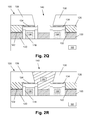
- FIG. 2Q depicts the product 100 after one or more etching processes were performed to remove the exposed portions of the first high-k protection layer 122 and the second high-k protection layer 134 selectively relative to surrounding materials.
- metal silicide regions (not shown) may be formed on the source/drain regions 120 .
- the metal silicide regions may be formed by performing traditional silicide formation techniques.
- FIG. 2R depicts the product 100 after a conductive, self-aligned contact structure 142 was formed in the self-aligned contact opening 140 such that it is conductively coupled to the source/drain region 120 .
- the self-aligned contact structure 142 is intended to be schematic and representative in nature, as it may be formed using any of a variety of different conductive materials and by performing traditional manufacturing operations.
- the self-aligned contact structure 142 may also contain one or more barrier layers (not depicted).
- the self-aligned contact structure 142 may be formed by depositing a liner, e.g., a titanium nitride liner, followed by overfilling the self-aligned contact opening 140 with a conductive material, such as tungsten. Thereafter, a CMP process may be performed to planarize the upper surface of the layer of insulating material 138 which results in the removal of excess portions of the liner and the tungsten positioned above the layer of insulating material 138 outside of the self-aligned contact opening 140 and the formation of the self-aligned contact structure 142 .
- a liner e.g., a titanium nitride liner
- FIGS. 3A-3H depict an embodiment wherein only the multi-layer gate cap structure 139 is formed for the product 100 , i.e., the first high-k protection layer 122 is omitted in this illustrative process flow. While not offering the complete protection as provided for by the combination of the first and second high-k protection layers 122 , 134 , the formation of just the novel multi-layer gate cap structure 139 provides significant protection in the important upper corner of the gate area, an area subjected to attack during normal contact formation process operations.
- FIG. 3A depicts the device 100 at a point in fabrication that corresponds to that shown in FIG. 2I except the formation and removal of parts of the first high-k protection layer 122 have been omitted. That is, FIG. 3A depicts the device 100 after the above-described replacement gate structures 130 were formed in the gate cavities 128 .
- FIG. 3B depicts the device 100 after the above-described recess etching process was performed on the spacers 118 such that the spacers 118 have a recessed upper surface 118 R.
- FIG. 3C depicts the device 100 after the above-described recess etching process was performed on the gate structures 130 such that the gate structures 130 have a recessed upper surface 130 R that is positioned below the recessed upper surface 118 R of the spacers 118 .
- FIG. 3D depicts the device 100 after the above-described HDP CVD-etching process was performed to form the above-described first gate cap material layer 132 .
- the HDP CVD-etching process is controlled such that the gate cap material layer 132 has an as-deposited, non-planar upper surface 132 S that defines a recess 132 R positioned above the gate structures 130 .
- FIG. 3E depicts the device 100 after the above-described second high-k protection layer 134 was conformably deposited on the non-planar upper surface 132 S of the first gate cap material layer 132 and after the above-described gate cap material layer 136 was deposited on the second high-k protection layer 134 so as to overfill the recesses 132 R.
- the “second” high-k protection layer 134 is the only protection layer formed, but it is still referred to as the second high-k protection layer to avoid confusion.
- FIG. 3F depicts the device 100 after one or more CMP processes were performed using the layer of insulating material 126 as a polish-stop layer. This operation removes portions of the first and second gate cap material layers 132 , 136 and portions of the second high-k protection layer 134 .
- a multi-layer gate cap structure 139 is provided above each of the gate structures 130 .
- the multi-layer gate cap structure 139 is comprised of the first gate cap material layer 132 , the second gate cap protection layer 134 and the second gate cap material layer 136 .
- FIG. 3G depicts the product 100 after the above-described layer of insulating material 138 was deposited across the product 100 above the multi-layer gate cap structures 139 .
- FIG. 3H depicts the product 100 after the above-described self-aligned contact opening 140 and self-aligned contact structure 142 were formed. Also note that, as depicted in the dashed-line region 141 , even if some of the multi-layer gate cap structure 139 is removed, i.e., a portion of the second gate cap material layer 136 , during the contact etch process, the underlying second high-k protection layer 134 still provides protection to the underlying gate structure 130 during the contact formation process.
Landscapes
- Engineering & Computer Science (AREA)
- Microelectronics & Electronic Packaging (AREA)
- Condensed Matter Physics & Semiconductors (AREA)
- General Physics & Mathematics (AREA)
- Computer Hardware Design (AREA)
- Physics & Mathematics (AREA)
- Power Engineering (AREA)
- Manufacturing & Machinery (AREA)
- Chemical & Material Sciences (AREA)
- Crystallography & Structural Chemistry (AREA)
- Internal Circuitry In Semiconductor Integrated Circuit Devices (AREA)
- Insulated Gate Type Field-Effect Transistor (AREA)
- Electrodes Of Semiconductors (AREA)
- Metal-Oxide And Bipolar Metal-Oxide Semiconductor Integrated Circuits (AREA)
Abstract
Description
- 1. Field of the Invention
- The present disclosure generally relates to the fabrication of integrated circuits, and, more particularly, to various methods of forming a protection layer on a semiconductor, and the resulting semiconductor device.
- 2. Description of the Related Art
- Generally, in complex circuitry including complex logic portions, MOS technology is presently a preferred manufacturing technique in view of device performance and/or power consumption and/or cost efficiency. In integrated circuits fabricated using MOS technology, field effect transistors (FETs), such as planar field effect transistors and/or FinFET transistors, are provided that are typically operated in a switched mode, i.e., these transistor devices exhibit a highly conductive state (on-state) and a high impedance state (off-state). The state of the field effect transistor is controlled by a gate electrode, which controls, upon application of an appropriate control voltage, the conductivity of a channel region formed between a drain region and a source region.
- To improve the operating speed of FETs, and to increase the density of FETs on an integrated circuit device, device designers have greatly reduced the physical size of FETs over the years. More specifically, the channel length of FETs has been significantly decreased, which has resulted in improving the switching speed of FETs. However, decreasing the channel length of a FET also decreases the distance between the source region and the drain region. In general, as a result of the reduced dimensions of the transistor devices, the operating speed of the circuit components has been increased with every new device generation, and the “packing density,” i.e., the number of transistor devices per unit area, in such products has also increased during that time. Such improvements in the performance of transistor devices has reached the point where one limiting factor relating to the operating speed of the final integrated circuit product is no longer the individual transistor element but the electrical performance of the complex wiring system that is formed above the device level that includes the actual semiconductor-based circuit elements.
- Typically, due to the large number of circuit elements and the required complex layout of modern integrated circuits, the electrical connections of the individual circuit elements cannot be established within the same device level on which the circuit elements are manufactured, but require one or more additional metallization layers, which generally include metal-containing lines providing the intra-level electrical connection, and also include a plurality of inter-level connections or vertical connections, which are also referred to as vias. These vertical interconnect structures comprise an appropriate metal and provide the electrical connection of the various stacked metallization layers.
- Furthermore, in order to actually connect the circuit elements formed in the semiconductor material with the metallization layers, an appropriate vertical contact structure is provided, a first lower end of which is connected to a respective contact region of a circuit element, such as a gate electrode and/or the drain and source regions of transistors, and a second end is connected to a respective metal line in the metallization layer by a conductive via. Such vertical contact structures are considered to be “device-level” contacts or simply “contacts” within the industry, as they contact the “device” that is formed in the silicon substrate. The contact structures may comprise contact elements or contact plugs having a generally square-like or round shape that are formed in an interlayer dielectric material, which in turn encloses and passivates the circuit elements. In other applications, the contact structures may be line-type features, e.g., source/drain contact structures.
- As device dimensions have decreased, e.g., transistors with gate lengths of 50 nm and less, the contact elements in the contact level have to be provided with critical dimensions on the same order of magnitude. The contact elements typically represent plugs, which are formed of an appropriate metal or metal composition, wherein, in sophisticated semiconductor devices, tungsten, in combination with appropriate barrier materials, has proven to be a viable contact metal. When forming tungsten-based contact elements, typically the interlayer dielectric material is formed first and is patterned so as to receive contact openings, which extend through the interlayer dielectric material to the corresponding contact areas of the circuit elements. In particular, in densely packed device regions, the lateral size of the drain and source areas and thus the available area for the contact regions is 100 nm and significantly less, thereby requiring extremely complex lithography and etch techniques in order to form the contact openings with well-defined lateral dimensions and with a high degree of alignment accuracy.
- For this reason, contact technologies have been developed in which contact openings are formed in a self-aligned manner by removing dielectric material, such as silicon dioxide, selectively from the spaces between closely spaced gate electrode structures. That is, after completing the transistor structure, at least the sidewall spacers of the gate electrode structures are used as etch masks for selectively removing the silicon dioxide material in order to expose the contact regions of the transistors, thereby providing self-aligned trenches which are substantially laterally delineated by the spacer structures of the gate electrode structures. Consequently, a corresponding lithography process only needs to define a global contact opening above an active region, wherein the contact trenches then result from the selective etch process using the spacer structures, i.e., the portions exposed by the global contact opening, as an etch mask. Thereafter, an appropriate contact material, such as tungsten and the like, may be filled into the contact trenches.
- However, the aforementioned process of forming self-aligned contacts results in an undesirable loss of at least portions of the spacer materials that protect the conductive gate electrode, as will be explained with reference to
FIGS. 1A-1B .FIG. 1A schematically illustrates a cross-sectional view of anintegrated circuit product 10 at an advanced manufacturing stage. As illustrated, theproduct 10 comprises a plurality ofillustrative gate structures 11 that are formed above asubstrate 12, such as a silicon substrate. Thegate structures 11 are comprised of an illustrativegate insulation layer 13 and anillustrative gate electrode 14. An illustrativegate cap layer 16 andsidewall spacers 18 encapsulate and protect thegate structures 11. Thegate cap layer 16 andsidewall spacers 18 are typically made of silicon nitride. Also depicted inFIG. 1A are a plurality of raised source/drain regions 20 and a layer ofinsulating material 22, e.g., silicon dioxide.FIG. 1B depicts theproduct 10 after anopening 24 has been formed in the layer of insulatingmaterial 22 for a self-aligned contact. Although the contact etch process performed to form theopening 24 is primarily directed at removing the desired portions of the layer ofinsulating material 22, portions of the protectivegate cap layer 16 and theprotective sidewall spacers 18 get consumed during the contact etch process, as simplistically depicted in thedashed regions 26. Given that thecap layer 16 and thespacers 18 are attacked in the contact etch process, the thickness of these protective materials must be sufficient such that, even after the contact etch process is completed, there remains sufficient material to protect thegate structures 11. Accordingly, device manufacturers tend to make thecap layers 16 andspacers 18 having an additional thickness that may otherwise not be required but for the consumption of thecap layers 16 and thespacers 18 during the contact etch process. In turn, increasing the thickness of such structures, i.e., increasing the thickness of thegate cap layers 16, causes other problems, such as increasing the aspect ratio of the contact opening 24 due to the increased height, increasing the initial gate height, which makes the gate etching and spacer etching processes more difficult, etc. Additionally, the source/drain regions 120 may also be subjected to undesirable attack during the contact formation process. - The present disclosure is directed to various methods of forming a protection layer on a semiconductor, and the resulting semiconductor device, that may avoid, or at least reduce, the effects of one or more of the problems identified above.
- The following presents a simplified summary of the invention in order to provide a basic understanding of some aspects of the invention. This summary is not an exhaustive overview of the invention. It is not intended to identify key or critical elements of the invention or to delineate the scope of the invention. Its sole purpose is to present some concepts in a simplified form as a prelude to the more detailed description that is discussed later.
- Generally, one aspect of the present disclosure is directed to various methods of forming a protection layer on a semiconductor, and the resulting semiconductor device. One illustrative method disclosed herein includes, among other things, forming a first high-k protection layer on the source/drain regions and adjacent the sidewall spacers of a transistor device, after forming the first high-k protection layer, removing a sacrificial gate structure positioned between the sidewall spacers so as to thereby define a replacement gate cavity between the sidewall spacers, forming a replacement gate structure in the replacement gate cavity, forming a second high-k protection layer above an upper surface of the spacers, above an upper surface of the replacement gate structure and above the first high-k protection layer, and removing portions of the second high-k protection layer positioned above the first high-k protection layer.
- Another aspect disclosed herein relates to forming a multi-layer gate cap structure. In one embodiment, the method includes, among other things, removing a sacrificial gate structure positioned between sidewall spacers of a device so as to thereby define a replacement gate cavity between the sidewall spacers, forming a replacement gate structure in a replacement gate cavity, forming a first gate cap material layer on the upper surface of the sidewall spacers and an upper surface of the replacement gate structure, wherein the first gate cap material layer has an as-deposited surface that defines a recess positioned above the replacement gate structure, forming a high-k protection layer on and in contact with the as-deposited surface of the first gate cap material layer in the recess above the replacement gate structure, forming a second gate cap material layer on the upper surface of the high-k protection layer, and removing portions of the second gate cap material layer, the high-k protection layer and first gate cap material layer positioned laterally outside of the spacers above the source/drain regions of the device so as to thereby define a multi-layer gate cap structure positioned above the recessed replacement gate structure, wherein the multi-layer gate cap structure is comprised of the first gate cap material layer, the high-k protection layer positioned on the first gate cap material layer and the second gate cap material layer positioned on the high-k protection layer.
- One illustrative example of a novel transistor device disclosed herein with a multi-layer gate cap structure includes, among other things, a gate structure, a spacer positioned adjacent opposite sides of the gate structure, and a multi-layer gate cap structure positioned above the gate structure and the upper surface of the spacers, wherein the multi-layer gate cap structure comprises a first gate cap material layer positioned on an upper surface of the gate structure and on the upper surface of the spacers, a high-k protection layer positioned on an upper surface of the first gate cap material layer and a second gate cap material layer positioned on an upper surface of the high-k protection layer.
- The disclosure may be understood by reference to the following description taken in conjunction with the accompanying drawings, in which like reference numerals identify like elements, and in which:
-
FIGS. 1A-1B schematically illustrate a cross-sectional view of an illustrative prior art integrated circuit product that employs self-aligned contacts; -
FIGS. 2A-2R depict various illustrative methods disclosed herein of forming a protection layer on a semiconductor, and the resulting semiconductor device; and -
FIGS. 3A-3H depict various novel methods disclosed herein for forming a multi-layer gate cap structure on a semiconductor device, and the resulting device. - While the subject matter disclosed herein is susceptible to various modifications and alternative forms, specific embodiments thereof have been shown by way of example in the drawings and are herein described in detail. It should be understood, however, that the description herein of specific embodiments is not intended to limit the invention to the particular forms disclosed, but on the contrary, the intention is to cover all modifications, equivalents, and alternatives falling within the spirit and scope of the invention as defined by the appended claims.
- Various illustrative embodiments of the invention are described below. In the interest of clarity, not all features of an actual implementation are described in this specification. It will of course be appreciated that in the development of any such actual embodiment, numerous implementation-specific decisions must be made to achieve the developers' specific goals, such as compliance with system-related and business-related constraints, which will vary from one implementation to another. Moreover, it will be appreciated that such a development effort might be complex and time-consuming, but would nevertheless be a routine undertaking for those of ordinary skill in the art having the benefit of this disclosure.
- The present subject matter will now be described with reference to the attached figures. Various structures, systems and devices are schematically depicted in the drawings for purposes of explanation only and so as to not obscure the present disclosure with details that are well known to those skilled in the art. Nevertheless, the attached drawings are included to describe and explain illustrative examples of the present disclosure. The words and phrases used herein should be understood and interpreted to have a meaning consistent with the understanding of those words and phrases by those skilled in the relevant art. No special definition of a term or phrase, i.e., a definition that is different from the ordinary and customary meaning as understood by those skilled in the art, is intended to be implied by consistent usage of the term or phrase herein. To the extent that a term or phrase is intended to have a special meaning, i.e., a meaning other than that understood by skilled artisans, such a special definition will be expressly set forth in the specification in a definitional manner that directly and unequivocally provides the special definition for the term or phrase.
- The present disclosure generally relates to various methods of forming a protection layer on a semiconductor, and the resulting semiconductor device. Moreover, as will be readily apparent to those skilled in the art upon a complete reading of the present application, the present method is applicable to a variety of devices, including, but not limited to, logic devices, memory devices, etc., and the methods disclosed herein may be employed to form N-type or P-type semiconductor devices. The methods and devices disclosed herein may be employed in manufacturing products using a variety of technologies, e.g., NMOS, PMOS, CMOS, etc., and they may be employed in manufacturing a variety of different devices, e.g., memory devices, logic devices, ASICs, etc. With reference to the attached figures, various illustrative embodiments of the methods and devices disclosed herein will now be described in more detail.
-
FIG. 2A schematically illustrates a cross-sectional view of anintegrated circuit product 100 at an advanced stage of manufacturing after several process operations were performed. As illustrated, theproduct 100 comprises a plurality of illustrative, and schematically depicted,sacrificial gate structures 111 that are formed above asubstrate 102. Also depicted are agate cap layer 113, sidewall spacers 118 (simplistically depicted) and raised source/drain regions 120. Thesubstrate 102 may have a variety of configurations, such as the depicted bulk substrate configuration. Thesubstrate 102 may have an SOI (silicon-on-insulator) configuration wherein the semiconductor devices are formed in the active layer of the SOI substrate. Thesubstrate 102 may be made of silicon or it may be made of materials other than silicon. Thus, the terms “substrate,” “semiconductor substrate” or “semiconducting substrate” should be understood to cover all semiconducting materials and all forms of such materials. The inventions disclosed herein will be disclosed in the context of forming planar transistor devices using a replacement gate process. However, as will be recognized by those skilled in the art after a complete reading of the present application, the inventions disclosed herein may be applied to the formation of planar FET devices as well as 3D devices, such as FinFET devices. Moreover, the methods disclosed herein are applicable to forming any type of device, e.g., an NFET device, a PFET device, etc. The various components and structures of the device disclosed herein may be formed using a variety of different materials and by performing a variety of known techniques, e.g., a chemical vapor deposition (CVD) process, an atomic layer deposition (ALD) process, a thermal growth process, spin-coating techniques, etc. The thicknesses of these various layers of material may also vary depending upon the particular application. - With continuing reference to
FIG. 2A , thesacrificial gate structures 111 are intended to be representative in nature of any type of sacrificial gate structure that may be employed in manufacturing integrated circuit products using so-called gate-last (replacement gate) manufacturing techniques. In general, thesacrificial gate structures 111 are comprised of a sacrificial gate insulation layer (not separately depicted), such as silicon dioxide, and a sacrificial gate electrode (not separately depicted), such as polysilicon or amorphous silicon. In one illustrative replacement gate manufacturing technique, the layers of material for the sacrificial gate structure including a gate cap layer (not shown) are initially formed/deposited above thesubstrate 102 and thereafter patterned using traditional masking and etching techniques to thereby define thesacrificial gate structure 111 with thegate cap layer 113 positioned above thesacrificial gate structure 111. Thereafter, thesidewall spacers 118 are formed adjacent the patterned dummy gate structure/cap layer. Thesacrificial gate structure 111 remains in place (protected by the spacers and the gate cap layer) as many process operations are performed to form the devices, e.g., the formation of the depicted raised, doped source/drain regions 120, performing an anneal process to repair damage to thesubstrate 102 caused by the ion implantation processes and to activate the implanted dopant materials. Thesidewall spacers 118 and thegate cap layer 113 may be made of materials such as silicon nitride. -
FIG. 2B depicts theproduct 100 after a first high-k protection layer 122 was conformably deposited on theproduct 100 by performing, for example, a conformal ALD or CVD process. In one illustrative embodiment, the first high-k protection layer 122 may be comprised of a material having a dielectric constant (k) greater than 7, e.g., hafnium oxide, aluminum oxide, SiCN, etc. The thickness of the first high-k protection layer 122 may vary depending upon the particular application, e.g., 2-6 nm. -
FIG. 2C depicts thedevice 100 after asacrificial material layer 124 was formed on thedevice 100. In one embodiment, thesacrificial material layer 124 is formed such that its upper surface is positioned above the cap layers 113. In one illustrative embodiment, thesacrificial material layer 124 may be comprised of OPL (Optical Planarization Layer), DUO™ oxide, etc. and it may be formed using traditional techniques for forming such materials, e.g., spin-coating, deposition, etc. -
FIG. 2D depicts thedevice 100 after a recess etching process was performed on thesacrificial material layer 124 to define a recessedsacrificial material layer 124R with a recessedupper surface 124X. After such recessing, the recessedsacrificial material layer 124R exposes portions, but not all, of the first high-k protection layer 122, i.e., the portion above thegate cap layer 113 and some of thelayer 122 positioned adjacent thespacers 118. The amount of the recessing depends upon the particular application. -
FIG. 2E depicts theproduct 100 after an etching process was performed to remove the exposed portions of the first high-k protection layer 122 selectively relative to surrounding materials. -
FIG. 2F depicts theproduct 100 after an etching process was performed to remove the recessedsacrificial material layer 124R selectively relative to surrounding materials. -
FIG. 2G depicts thedevice 100 after several process operations were performed. First, a layer of insulatingmaterial 126 was deposited so as to over-fill the spaces between thespacers 118. Thereafter, one or more chemical mechanical polishing (CMP) processes were performed to remove the gate cap layers 113 so as to expose theupper surface 111S, i.e., the dummy gate electrode (polysilicon), of thesacrificial gate structure 111. -
FIG. 2H depicts theproduct 100 after one or more etching processes were performed to remove thesacrificial gate structure 111 which results in the formation of areplacement gate cavity 128 that is laterally defined by thespacers 118 where the final replacement gate structure for the devices will be formed. -
FIG. 2I depicts thedevice 100 after illustrative and schematically depicted replacement (final)gate structures 130 were formed in thegate cavities 128. Thegate structures 130 depicted herein are intended to be representative in nature of any type of replacement gate structure that may be employed in manufacturing integrated circuit products. Typically, a pre-clean process will be performed in an attempt to remove all foreign materials from within thegate cavities 128 prior to forming the various layers of material that will become part of thegate structures 130. Thereafter, thegate structures 130 may be formed by sequentially depositing the materials of the gate structures into thegate cavities 128 and above the layer of insulatingmaterial 126 and then performing a CMP process to remove excess materials above the layer of insulatingmaterial 126. -
FIG. 2J depicts thedevice 100 after a recess etching process was performed on thespacers 118 such that thespacers 118 have a recessedupper surface 118R. The amount or extent of recessing of thespacers 118 may vary depending upon the particular application, e.g., 30-50 nm. -
FIG. 2K depicts thedevice 100 after a recess etching process was performed on thegate structures 130 such that thegate structures 130 have a recessedupper surface 130R that is positioned below the recessedupper surface 118R of thespacers 118. The amount or extent of recessing of thegate structures 130 may vary depending upon the particular application. However, the recessing of thegate structures 130 need not be performed in all applications. That is, in some applications, the upper surface of thegate structures 130 may be at about the same level or slightly above the recessed surfaces 118R of thespacers 118. -
FIG. 2L depicts thedevice 100 after a high density plasma CVD and etching process operation (hereinafter “HDP CVD-etching process”) was performed to form a first gatecap material layer 132. In general, the HDP CVD-etching process is a combination of deposition/etch cycles that result in the first gatecap material layer 132 having an as-deposited, non-planarupper surface 132S. The HDP CVD-etching process typically involves performing a series of CVD deposition and etching processes in a common process chamber without breaking vacuum or transferring the wafer to another chamber, e.g., deposition-etch-deposition-etch, etc. The number and duration of the deposition-etch sequences performed in the HDP CVD-etching process may vary depending upon the particular application and they may vary depending upon factors such as the depth and CD of the opening into which the material is to be deposited. The precise parameters of the HDP CVD-etching process for any particular application may need to be determined based upon experimentation and testing techniques that are within the skill level of those skilled in the art. In one embodiment, the HDP CVD-etching process involves use of SiH4, N2/NH3 and Ar, where the argon has a sputtering type effect at the same time CVD film deposition is occurring. In one embodiment, during the etching portion of the HDP CVD-etching process, NF3 is used as an etchant gas. However, using the HDP CVD-etching process described herein, the top corner region of an opening, i.e., the region where overhang normally occurs during a standard CVD process, was etched more than the regions inside the opening. The combination of the NF3 etching and the argon sputtering, along with the deposition sequencing, resulted in the first gatecap material layer 132 having the as-deposited, non-planarupper surface 132S. In one embodiment, the first gatecap material layer 132 may be made of an HDP silicon nitride, SiCN, SiBN, etc. The thickness of the first gatecap material layer 132 may vary depending upon the particular application. -
FIG. 2M depicts thedevice 100 after several process operations were performed. First, a second high-k protection layer 134 was conformably deposited on theproduct 100 by performing, for example, a conformal ALD or CVD process. Due to the non-planarupper surface 132S of the first gatecap material layer 132, the second high-k protection layer 134 also has a non-planar upper surface. After the formation of the second high-k protection layer 134, portions of therecess 132R remain unfilled above the second high-k protection layer 134. Thereafter, a second gatecap material layer 136 was deposited on the non-planar upper surface of the second high-k protection layer 134 so as to overfill the remaining portion of therecesses 132R. In one illustrative embodiment, the second high-k protection layer 134 may be comprised of a material having a dielectric constant (k) greater than 7, e.g., hafnium oxide, aluminum oxide, SiCN, etc. The thickness of the second high-k protection layer 134 may vary depending upon the particular application, e.g., 2-6 nm. In one embodiment, the second high-k protection layer 134 may be made of the same material as that of the first high-k protection layer 122. The second gatecap material layer 136 may be comprised of the same materials as those of the first gatecap material layer 132. -
FIG. 2N depicts thedevice 100 after one or more CMP processes were performed using the layer of insulatingmaterial 126 as a polish-stop layer. This operation removes portions of the first and second gate cap material layers 132, 136 and portions of the second high-k protection layer 132 in areas laterally outside thespacers 118, i.e., the materials are removed from above the source/drain regions 120. Importantly, as depicted, the combination of the first and second high-k protection layers 122, 134 substantially encapsulate or cover thegate structures 130, thesidewall spacers 118 and the epi source/drain regions 120, thereby providing a very high degree of protection, if not absolute protection, to these structures of the transistor devices during subsequent contact formation processes (to be discussed more fully below). Additionally, as a result of the processing described above, a multi-layergate cap structure 139 is provided above each of thegate structures 130. In the depicted example, the multi-layergate cap structure 139 is comprised of the first gatecap material layer 132, the second gatecap protection layer 134 and the second gatecap material layer 136. -
FIG. 2O depicts theproduct 100 after a layer of insulatingmaterial 138 was deposited across theproduct 100. The layer of insulatingmaterial 138 may be comprised of a variety of different materials, such as silicon dioxide, etc., and it may be formed by performing a variety of techniques, e.g., CVD, etc. The thickness of the layer of insulatingmaterial 138 may vary depending upon the particular application. The layer of insulatingmaterial 138 may be comprised of the same or different materials as that of the layer of insulatingmaterial 126. -
FIG. 2P depicts theproduct 100 after one or more etching processes were performed on theproduct 100 through a patterned etch mask (not shown), such as a patterned layer of photoresist material, to thereby define a self-alignedcontact opening 140.Such contact openings 140 would be formed above all of the source/drain regions 120 on theproduct 100, but the drawings only depict the formation of thecontact opening 140 between the twogate structures 130 so as not to overly complicate the drawings. The formation of thecontact opening 140 removes substantially all of the exposed portions of the layer of insulatingmaterial 126 positioned above the source/drain region 120. Importantly, the combination of the first and second high-k protection layers 122, 134 serves as a very etch resistant etch stop layer during the process of forming thecontact opening 140, thereby offering substantially complete protection to thegate structures 130, thespacers 118 and the source/drain regions 120 during the contact opening etching processes. Also note that, as depicted in the dashed-line region 141, even if some of the multi-layergate cap structure 139 is removed during the contact etch process, such as a portion of the second gatecap material layer 136, the underlying second high-k protection layer 134 still provides protection to theunderlying gate structure 130. -
FIG. 2Q depicts theproduct 100 after one or more etching processes were performed to remove the exposed portions of the first high-k protection layer 122 and the second high-k protection layer 134 selectively relative to surrounding materials. At this point in the process flow, metal silicide regions (not shown) may be formed on the source/drain regions 120. The metal silicide regions may be formed by performing traditional silicide formation techniques. -
FIG. 2R depicts theproduct 100 after a conductive, self-alignedcontact structure 142 was formed in the self-aligned contact opening 140 such that it is conductively coupled to the source/drain region 120. The self-alignedcontact structure 142 is intended to be schematic and representative in nature, as it may be formed using any of a variety of different conductive materials and by performing traditional manufacturing operations. The self-alignedcontact structure 142 may also contain one or more barrier layers (not depicted). In one illustrative example, the self-alignedcontact structure 142 may be formed by depositing a liner, e.g., a titanium nitride liner, followed by overfilling the self-aligned contact opening 140 with a conductive material, such as tungsten. Thereafter, a CMP process may be performed to planarize the upper surface of the layer of insulatingmaterial 138 which results in the removal of excess portions of the liner and the tungsten positioned above the layer of insulatingmaterial 138 outside of the self-alignedcontact opening 140 and the formation of the self-alignedcontact structure 142. -
FIGS. 3A-3H depict an embodiment wherein only the multi-layergate cap structure 139 is formed for theproduct 100, i.e., the first high-k protection layer 122 is omitted in this illustrative process flow. While not offering the complete protection as provided for by the combination of the first and second high-k protection layers 122, 134, the formation of just the novel multi-layergate cap structure 139 provides significant protection in the important upper corner of the gate area, an area subjected to attack during normal contact formation process operations. -
FIG. 3A depicts thedevice 100 at a point in fabrication that corresponds to that shown inFIG. 2I except the formation and removal of parts of the first high-k protection layer 122 have been omitted. That is,FIG. 3A depicts thedevice 100 after the above-describedreplacement gate structures 130 were formed in thegate cavities 128. -
FIG. 3B depicts thedevice 100 after the above-described recess etching process was performed on thespacers 118 such that thespacers 118 have a recessedupper surface 118R. -
FIG. 3C depicts thedevice 100 after the above-described recess etching process was performed on thegate structures 130 such that thegate structures 130 have a recessedupper surface 130R that is positioned below the recessedupper surface 118R of thespacers 118. -
FIG. 3D depicts thedevice 100 after the above-described HDP CVD-etching process was performed to form the above-described first gatecap material layer 132. As before, the HDP CVD-etching process is controlled such that the gatecap material layer 132 has an as-deposited, non-planarupper surface 132S that defines arecess 132R positioned above thegate structures 130. -
FIG. 3E depicts thedevice 100 after the above-described second high-k protection layer 134 was conformably deposited on the non-planarupper surface 132S of the first gatecap material layer 132 and after the above-described gatecap material layer 136 was deposited on the second high-k protection layer 134 so as to overfill therecesses 132R. Of course, in this embodiment, the “second” high-k protection layer 134 is the only protection layer formed, but it is still referred to as the second high-k protection layer to avoid confusion. -
FIG. 3F depicts thedevice 100 after one or more CMP processes were performed using the layer of insulatingmaterial 126 as a polish-stop layer. This operation removes portions of the first and second gate cap material layers 132, 136 and portions of the second high-k protection layer 134. As noted above, as a result of the processing described above, a multi-layergate cap structure 139 is provided above each of thegate structures 130. In the depicted example, the multi-layergate cap structure 139 is comprised of the first gatecap material layer 132, the second gatecap protection layer 134 and the second gatecap material layer 136. -
FIG. 3G depicts theproduct 100 after the above-described layer of insulatingmaterial 138 was deposited across theproduct 100 above the multi-layergate cap structures 139. -
FIG. 3H depicts theproduct 100 after the above-described self-alignedcontact opening 140 and self-alignedcontact structure 142 were formed. Also note that, as depicted in the dashed-line region 141, even if some of the multi-layergate cap structure 139 is removed, i.e., a portion of the second gatecap material layer 136, during the contact etch process, the underlying second high-k protection layer 134 still provides protection to theunderlying gate structure 130 during the contact formation process. - The particular embodiments disclosed above are illustrative only, as the invention may be modified and practiced in different but equivalent manners apparent to those skilled in the art having the benefit of the teachings herein. For example, the process steps set forth above may be performed in a different order. Furthermore, no limitations are intended to the details of construction or design herein shown, other than as described in the claims below. It is therefore evident that the particular embodiments disclosed above may be altered or modified and all such variations are considered within the scope and spirit of the invention. Note that the use of terms, such as “first,” “second,” “third” or “fourth” to describe various processes or structures in this specification and in the attached claims is only used as a shorthand reference to such steps/structures and does not necessarily imply that such steps/structures are performed/formed in that ordered sequence. Of course, depending upon the exact claim language, an ordered sequence of such processes may or may not be required. Accordingly, the protection sought herein is as set forth in the claims below.
Claims (22)
Priority Applications (2)
| Application Number | Priority Date | Filing Date | Title |
|---|---|---|---|
| US14/301,864 US9634115B2 (en) | 2014-06-11 | 2014-06-11 | Methods of forming a protection layer on a semiconductor device and the resulting device |
| US15/451,565 US10249726B2 (en) | 2014-06-11 | 2017-03-07 | Methods of forming a protection layer on a semiconductor device and the resulting device |
Applications Claiming Priority (1)
| Application Number | Priority Date | Filing Date | Title |
|---|---|---|---|
| US14/301,864 US9634115B2 (en) | 2014-06-11 | 2014-06-11 | Methods of forming a protection layer on a semiconductor device and the resulting device |
Related Child Applications (1)
| Application Number | Title | Priority Date | Filing Date |
|---|---|---|---|
| US15/451,565 Division US10249726B2 (en) | 2014-06-11 | 2017-03-07 | Methods of forming a protection layer on a semiconductor device and the resulting device |
Publications (2)
| Publication Number | Publication Date |
|---|---|
| US20150364326A1 true US20150364326A1 (en) | 2015-12-17 |
| US9634115B2 US9634115B2 (en) | 2017-04-25 |
Family
ID=54836753
Family Applications (2)
| Application Number | Title | Priority Date | Filing Date |
|---|---|---|---|
| US14/301,864 Active 2034-08-10 US9634115B2 (en) | 2014-06-11 | 2014-06-11 | Methods of forming a protection layer on a semiconductor device and the resulting device |
| US15/451,565 Active 2034-08-07 US10249726B2 (en) | 2014-06-11 | 2017-03-07 | Methods of forming a protection layer on a semiconductor device and the resulting device |
Family Applications After (1)
| Application Number | Title | Priority Date | Filing Date |
|---|---|---|---|
| US15/451,565 Active 2034-08-07 US10249726B2 (en) | 2014-06-11 | 2017-03-07 | Methods of forming a protection layer on a semiconductor device and the resulting device |
Country Status (1)
| Country | Link |
|---|---|
| US (2) | US9634115B2 (en) |
Cited By (24)
| Publication number | Priority date | Publication date | Assignee | Title |
|---|---|---|---|---|
| US20160064293A1 (en) * | 2014-08-29 | 2016-03-03 | Taiwan Semiconductor Manufacturing Company Limited | Semiconductor arrangement and formation thereof |
| US20160126326A1 (en) * | 2014-10-29 | 2016-05-05 | Sungil Park | Semiconductor Devices Including Contact Patterns Having a Rising Portion and a Recessed Portion |
| US20160190263A1 (en) * | 2014-06-11 | 2016-06-30 | Globalfoundries Inc. | Devices formed by performing a common etch patterning process to form gate and source/drain contact openings |
| US9548366B1 (en) * | 2016-04-04 | 2017-01-17 | Taiwan Semiconductor Manufacturing Company, Ltd. | Self aligned contact scheme |
| US20170040179A1 (en) * | 2015-08-03 | 2017-02-09 | United Microelectronics Corp. | Method for fabricating semiconductor device |
| US9627509B2 (en) * | 2014-07-21 | 2017-04-18 | Samsung Electronics Co., Ltd. | Semiconductor device and method of fabricating the same |
| US20170194499A1 (en) * | 2015-11-25 | 2017-07-06 | International Business Machines Corporation | Replacement low-k spacer |
| US20170256568A1 (en) * | 2016-03-04 | 2017-09-07 | Taiwan Semiconductor Manufacturing Co., Ltd. | Semiconductor device and a method for fabricating the same |
| US20170294535A1 (en) * | 2016-04-08 | 2017-10-12 | Semiconductor Manufacturing International (Shanghai) Corporation | Semiconductor device and fabrication method thereof |
| US20170317079A1 (en) * | 2016-04-28 | 2017-11-02 | Samsung Electronics Co., Ltd. | Semiconductor device and method of manufacturing the same |
| US20170317076A1 (en) * | 2016-04-28 | 2017-11-02 | Taiwan Semiconductor Manufacturing Co., Ltd. | Semiconductor device and a method for fabricating the same |
| EP3267474A1 (en) * | 2016-07-04 | 2018-01-10 | Semiconductor Manufacturing International Corporation (Shanghai) | Contact structure and associated method for flash memory |
| US9947589B1 (en) * | 2017-05-22 | 2018-04-17 | Globalfoundries Inc. | Methods of forming a gate contact for a transistor above an active region and the resulting device |
| US10002933B1 (en) * | 2017-03-27 | 2018-06-19 | Taiwan Semiconductor Manufacturing Co., Ltd. | Semiconductor device structure with cap layer with top and bottom portions over gate electrode |
| US10056473B1 (en) * | 2017-04-07 | 2018-08-21 | Taiwan Semiconductor Manufacturing Co., Ltd. | Semiconductor device and manufacturing method thereof |
| US20180294184A1 (en) * | 2017-04-07 | 2018-10-11 | Taiwan Semiconductor Manufacturing Company, Ltd. | Low-Resistance Contact Plugs and Method Forming Same |
| US10109524B2 (en) * | 2017-01-24 | 2018-10-23 | Globalfoundries Inc. | Recessing of liner and conductor for via formation |
| US20190165114A1 (en) * | 2017-11-29 | 2019-05-30 | Samsung Electronics Co., Ltd. | Semiconductor device and method of manufacturing the same |
| US10347726B2 (en) * | 2017-04-03 | 2019-07-09 | Samsung Electronics Co., Ltd. | Semiconductor device having shared contact |
| US20200105597A1 (en) * | 2018-10-02 | 2020-04-02 | Globalfoundries Inc. | Methods, apparatus and system for a local interconnect feature over an active region in a finfet device |
| US20210225701A1 (en) * | 2017-11-30 | 2021-07-22 | Taiwan Semiconductor Manufacturing Co., Ltd. | Conductive Feature Formation and Structure |
| US11355634B2 (en) * | 2019-01-31 | 2022-06-07 | Semiconductor Manufacturing International (Shanghai) Corporation | Semiconductor device and fabrication method thereof |
| TWI785589B (en) * | 2020-10-15 | 2022-12-01 | 台灣積體電路製造股份有限公司 | Semiconductor device and method of forming same |
| US12020981B2 (en) | 2017-11-30 | 2024-06-25 | Taiwan Semiconductor Manufacturing Co., Ltd. | Conductive feature formation and structure |
Families Citing this family (9)
| Publication number | Priority date | Publication date | Assignee | Title |
|---|---|---|---|---|
| US9799748B1 (en) * | 2017-01-04 | 2017-10-24 | Globalfoundries Inc. | Method of forming inner spacers on a nano-sheet/wire device |
| US10170377B1 (en) | 2017-09-20 | 2019-01-01 | Globalfoundries Inc. | Memory cell with recessed source/drain contacts to reduce capacitance |
| US10396155B2 (en) | 2017-09-20 | 2019-08-27 | Globalfoundries Inc. | Semiconductor device with recessed source/drain contacts and a gate contact positioned above the active region |
| US10957543B2 (en) * | 2017-09-29 | 2021-03-23 | Taiwan Semiconductor Manufacturing Co., Ltd. | Device and method of dielectric layer |
| US10243053B1 (en) * | 2018-01-22 | 2019-03-26 | Globalfoundries Inc. | Gate contact structure positioned above an active region of a transistor device |
| US10559470B2 (en) * | 2018-01-22 | 2020-02-11 | Globalfoundries Inc. | Capping structure |
| US10685872B2 (en) * | 2018-05-30 | 2020-06-16 | International Business Machines Corporation | Electrically isolated contacts in an active region of a semiconductor device |
| CN111697073B (en) * | 2019-03-15 | 2023-07-14 | 中芯国际集成电路制造(上海)有限公司 | Semiconductor structure and forming method thereof |
| KR20220005746A (en) * | 2020-07-07 | 2022-01-14 | 삼성전자주식회사 | Semiconductor device |
Citations (2)
| Publication number | Priority date | Publication date | Assignee | Title |
|---|---|---|---|---|
| US20100090321A1 (en) * | 2008-10-10 | 2010-04-15 | Robert Mulfinger | High-k etch stop layer of reduced thickness for patterning a dielectric material during fabrication of transistors |
| US20140103403A1 (en) * | 2012-10-12 | 2014-04-17 | Samsung Electronics Co., Ltd. | Method for manufacturing semiconductor device |
Family Cites Families (1)
| Publication number | Priority date | Publication date | Assignee | Title |
|---|---|---|---|---|
| US20130181265A1 (en) * | 2012-01-18 | 2013-07-18 | Globalfoundries Inc. | Methods of Forming a Gate Cap Layer Above a Replacement Gate Structure and a Semiconductor Device That Includes Such a Gate Structure and Cap Layer |
-
2014
- 2014-06-11 US US14/301,864 patent/US9634115B2/en active Active
-
2017
- 2017-03-07 US US15/451,565 patent/US10249726B2/en active Active
Patent Citations (2)
| Publication number | Priority date | Publication date | Assignee | Title |
|---|---|---|---|---|
| US20100090321A1 (en) * | 2008-10-10 | 2010-04-15 | Robert Mulfinger | High-k etch stop layer of reduced thickness for patterning a dielectric material during fabrication of transistors |
| US20140103403A1 (en) * | 2012-10-12 | 2014-04-17 | Samsung Electronics Co., Ltd. | Method for manufacturing semiconductor device |
Cited By (59)
| Publication number | Priority date | Publication date | Assignee | Title |
|---|---|---|---|---|
| US20160190263A1 (en) * | 2014-06-11 | 2016-06-30 | Globalfoundries Inc. | Devices formed by performing a common etch patterning process to form gate and source/drain contact openings |
| US9627509B2 (en) * | 2014-07-21 | 2017-04-18 | Samsung Electronics Co., Ltd. | Semiconductor device and method of fabricating the same |
| US20160322268A1 (en) * | 2014-08-29 | 2016-11-03 | Taiwan Semiconductor Manufacturing Company Limited | Semiconductor arrangement and formation thereof |
| US9390985B2 (en) * | 2014-08-29 | 2016-07-12 | Taiwan Semiconductor Manufacturing Company Limited | Semiconductor arrangement and formation thereof |
| US20160064293A1 (en) * | 2014-08-29 | 2016-03-03 | Taiwan Semiconductor Manufacturing Company Limited | Semiconductor arrangement and formation thereof |
| US9748152B2 (en) * | 2014-08-29 | 2017-08-29 | Taiwan Semiconductor Manufacturing Company Limited | Semiconductor arrangement and formation thereof |
| US9536968B2 (en) * | 2014-10-29 | 2017-01-03 | Samsung Electronics Co., Ltd. | Semiconductor devices including contact patterns having a rising portion and a recessed portion |
| US20160126326A1 (en) * | 2014-10-29 | 2016-05-05 | Sungil Park | Semiconductor Devices Including Contact Patterns Having a Rising Portion and a Recessed Portion |
| US9941161B2 (en) * | 2015-08-03 | 2018-04-10 | United Microelectronics Corp. | Method for fabricating semiconductor device |
| US20170040179A1 (en) * | 2015-08-03 | 2017-02-09 | United Microelectronics Corp. | Method for fabricating semiconductor device |
| US9985135B2 (en) * | 2015-11-25 | 2018-05-29 | International Business Machines Corporation | Replacement low-k spacer |
| US20170194499A1 (en) * | 2015-11-25 | 2017-07-06 | International Business Machines Corporation | Replacement low-k spacer |
| US20170256568A1 (en) * | 2016-03-04 | 2017-09-07 | Taiwan Semiconductor Manufacturing Co., Ltd. | Semiconductor device and a method for fabricating the same |
| US10056407B2 (en) * | 2016-03-04 | 2018-08-21 | Taiwan Semiconductor Manufacturing Co., Ltd | Semiconductor device and a method for fabricating the same |
| TWI596705B (en) * | 2016-04-04 | 2017-08-21 | 台灣積體電路製造股份有限公司 | Semiconductor device and method for manufacturing the same |
| US9859386B2 (en) | 2016-04-04 | 2018-01-02 | Taiwan Semiconductor Manufacturing Company, Ltd. | Self aligned contact scheme |
| US9548366B1 (en) * | 2016-04-04 | 2017-01-17 | Taiwan Semiconductor Manufacturing Company, Ltd. | Self aligned contact scheme |
| US20170294535A1 (en) * | 2016-04-08 | 2017-10-12 | Semiconductor Manufacturing International (Shanghai) Corporation | Semiconductor device and fabrication method thereof |
| US10797048B2 (en) * | 2016-04-28 | 2020-10-06 | Taiwan Semiconductor Manufacturing Co., Ltd. | Semiconductor device and a method for fabricating the same |
| US20170317079A1 (en) * | 2016-04-28 | 2017-11-02 | Samsung Electronics Co., Ltd. | Semiconductor device and method of manufacturing the same |
| US10553582B2 (en) * | 2016-04-28 | 2020-02-04 | Samsung Electronics Co., Ltd. | Semiconductor device and method of manufacturing the same |
| US20180138176A1 (en) * | 2016-04-28 | 2018-05-17 | Taiwan Semiconductor Manufacturing Co., Ltd. | Semiconductor device and a method for fabricating the same |
| US9893062B2 (en) * | 2016-04-28 | 2018-02-13 | Taiwan Semiconductor Manufacturing Co., Ltd. | Semiconductor device and a method for fabricating the same |
| US10797051B2 (en) | 2016-04-28 | 2020-10-06 | Samsung Electronics Co., Ltd. | Semiconductor device and method of manufacturing the same |
| US20170317076A1 (en) * | 2016-04-28 | 2017-11-02 | Taiwan Semiconductor Manufacturing Co., Ltd. | Semiconductor device and a method for fabricating the same |
| US11521970B2 (en) | 2016-04-28 | 2022-12-06 | Taiwan Semiconductor Manufacturing Co., Ltd. | Semiconductor device and a method for fabricating the same |
| EP3267474A1 (en) * | 2016-07-04 | 2018-01-10 | Semiconductor Manufacturing International Corporation (Shanghai) | Contact structure and associated method for flash memory |
| US10763169B2 (en) | 2016-07-04 | 2020-09-01 | Semiconductor Manufacturing International (Shanghai) Corporation | Contact structure and associated method for flash memory |
| US10242910B2 (en) | 2016-07-04 | 2019-03-26 | Semiconductor Manufacturing International (Shanghai) Corporation | Contact structure and associated method for flash memory |
| US10109524B2 (en) * | 2017-01-24 | 2018-10-23 | Globalfoundries Inc. | Recessing of liner and conductor for via formation |
| US10002933B1 (en) * | 2017-03-27 | 2018-06-19 | Taiwan Semiconductor Manufacturing Co., Ltd. | Semiconductor device structure with cap layer with top and bottom portions over gate electrode |
| US10998411B2 (en) | 2017-04-03 | 2021-05-04 | Samsung Electronics Co., Ltd. | Semiconductor device |
| US10347726B2 (en) * | 2017-04-03 | 2019-07-09 | Samsung Electronics Co., Ltd. | Semiconductor device having shared contact |
| US11901422B2 (en) | 2017-04-03 | 2024-02-13 | Samsung Electronics Co., Ltd. | Semiconductor device having fin-type active patterns with shared contact plugs |
| US10741438B2 (en) | 2017-04-07 | 2020-08-11 | Taiwan Semiconductor Manufacturing Company, Ltd. | Low-resistance contact plugs and method forming the same |
| US20180294184A1 (en) * | 2017-04-07 | 2018-10-11 | Taiwan Semiconductor Manufacturing Company, Ltd. | Low-Resistance Contact Plugs and Method Forming Same |
| US12068191B2 (en) | 2017-04-07 | 2024-08-20 | Taiwan Semiconductor Manufacturing Company, Ltd. | Low-resistance contact plugs and method forming same |
| US10720514B2 (en) * | 2017-04-07 | 2020-07-21 | Taiwan Semiconductor Manufacturing Co., Ltd. | Semiconductor device and manufacturing method thereof |
| US11532504B2 (en) | 2017-04-07 | 2022-12-20 | Taiwan Semiconductor Manufacturing Company, Ltd. | Low-resistance contact plugs and method forming same |
| US20190013396A1 (en) * | 2017-04-07 | 2019-01-10 | Taiwan Semiconductor Manufacturing Co., Ltd. | Semiconductor device and manufacturing method thereof |
| US10153198B2 (en) * | 2017-04-07 | 2018-12-11 | Taiwan Semiconductor Manufacturing Company, Ltd. | Low-resistance contact plugs and method forming same |
| CN108695240A (en) * | 2017-04-07 | 2018-10-23 | 台湾积体电路制造股份有限公司 | The forming method of low resistance contacts window plug |
| US10056473B1 (en) * | 2017-04-07 | 2018-08-21 | Taiwan Semiconductor Manufacturing Co., Ltd. | Semiconductor device and manufacturing method thereof |
| US11043579B2 (en) | 2017-04-07 | 2021-06-22 | Taiwan Semiconductor Manufacturing Co., Ltd. | Method for manufacturing semiconductor device |
| US9947589B1 (en) * | 2017-05-22 | 2018-04-17 | Globalfoundries Inc. | Methods of forming a gate contact for a transistor above an active region and the resulting device |
| US11557656B2 (en) * | 2017-11-29 | 2023-01-17 | Samsung Electronics Co., Ltd. | Semiconductor device having a capping pattern on a gate electrode |
| US20190165114A1 (en) * | 2017-11-29 | 2019-05-30 | Samsung Electronics Co., Ltd. | Semiconductor device and method of manufacturing the same |
| CN109841673A (en) * | 2017-11-29 | 2019-06-04 | 三星电子株式会社 | Semiconductor device and its manufacturing method |
| KR20190063097A (en) * | 2017-11-29 | 2019-06-07 | 삼성전자주식회사 | Semiconductor device and method for manufacturing the same |
| KR102432866B1 (en) * | 2017-11-29 | 2022-08-17 | 삼성전자주식회사 | Semiconductor device and method for manufacturing the same |
| US10811505B2 (en) * | 2017-11-29 | 2020-10-20 | Samsung Electronics Co., Ltd. | Gate electrode having upper and lower capping patterns |
| US11798843B2 (en) * | 2017-11-30 | 2023-10-24 | Taiwan Semiconductor Manufacturing Co., Ltd. | Conductive feature formation and structure |
| US12020981B2 (en) | 2017-11-30 | 2024-06-25 | Taiwan Semiconductor Manufacturing Co., Ltd. | Conductive feature formation and structure |
| US20210225701A1 (en) * | 2017-11-30 | 2021-07-22 | Taiwan Semiconductor Manufacturing Co., Ltd. | Conductive Feature Formation and Structure |
| US10937693B2 (en) * | 2018-10-02 | 2021-03-02 | Globalfoundries Inc. | Methods, apparatus and system for a local interconnect feature over an active region in a finFET device |
| US20200105597A1 (en) * | 2018-10-02 | 2020-04-02 | Globalfoundries Inc. | Methods, apparatus and system for a local interconnect feature over an active region in a finfet device |
| US11355634B2 (en) * | 2019-01-31 | 2022-06-07 | Semiconductor Manufacturing International (Shanghai) Corporation | Semiconductor device and fabrication method thereof |
| TWI785589B (en) * | 2020-10-15 | 2022-12-01 | 台灣積體電路製造股份有限公司 | Semiconductor device and method of forming same |
| US11894435B2 (en) | 2020-10-15 | 2024-02-06 | Taiwan Semiconductor Manufacturing Co., Ltd. | Contact plug structure of semiconductor device and method of forming same |
Also Published As
| Publication number | Publication date |
|---|---|
| US20170179246A1 (en) | 2017-06-22 |
| US10249726B2 (en) | 2019-04-02 |
| US9634115B2 (en) | 2017-04-25 |
Similar Documents
| Publication | Publication Date | Title |
|---|---|---|
| US10249726B2 (en) | Methods of forming a protection layer on a semiconductor device and the resulting device | |
| US9312182B2 (en) | Forming gate and source/drain contact openings by performing a common etch patterning process | |
| US8928048B2 (en) | Methods of forming semiconductor device with self-aligned contact elements and the resulting device | |
| US8906754B2 (en) | Methods of forming a semiconductor device with a protected gate cap layer and the resulting device | |
| US9530866B1 (en) | Methods of forming vertical transistor devices with self-aligned top source/drain conductive contacts | |
| US9466491B2 (en) | Methods of forming a semiconductor device with a spacer etch block cap and the resulting device | |
| US9455254B2 (en) | Methods of forming a combined gate and source/drain contact structure and the resulting device | |
| US8841711B1 (en) | Methods of increasing space for contact elements by using a sacrificial liner and the resulting device | |
| US9553028B2 (en) | Methods of forming reduced resistance local interconnect structures and the resulting devices | |
| US9536877B2 (en) | Methods of forming different spacer structures on integrated circuit products having differing gate pitch dimensions and the resulting products | |
| US9515163B2 (en) | Methods of forming FinFET semiconductor devices with self-aligned contact elements using a replacement gate process and the resulting devices | |
| US8846513B2 (en) | Semiconductor device comprising replacement gate electrode structures and self-aligned contact elements formed by a late contact fill | |
| US9502286B2 (en) | Methods of forming self-aligned contact structures on semiconductor devices and the resulting devices | |
| US8871582B2 (en) | Methods of forming a semiconductor device with a protected gate cap layer and the resulting device | |
| US10276674B2 (en) | Method of forming a gate contact structure and source/drain contact structure for a semiconductor device | |
| US8946075B2 (en) | Methods of forming semiconductor device with self-aligned contact elements and the resulting devices | |
| US9824920B2 (en) | Methods of forming self-aligned contact structures by work function material layer recessing and the resulting devices | |
| US9461171B2 (en) | Methods of increasing silicide to epi contact areas and the resulting devices | |
| US10468300B2 (en) | Contacting source and drain of a transistor device | |
| US8940633B2 (en) | Methods of forming semiconductor device with self-aligned contact elements and the resulting devices | |
| US10396155B2 (en) | Semiconductor device with recessed source/drain contacts and a gate contact positioned above the active region | |
| US20170345912A1 (en) | Methods of recessing a gate structure using oxidizing treatments during a recessing etch process | |
| CN109300780B (en) | Method of forming conductive spacers for gate contact and resulting device | |
| US9947589B1 (en) | Methods of forming a gate contact for a transistor above an active region and the resulting device | |
| US9627274B1 (en) | Methods of forming self-aligned contacts on FinFET devices |
Legal Events
| Date | Code | Title | Description |
|---|---|---|---|
| AS | Assignment |
Owner name: GLOBALFOUNDRIES INC., CAYMAN ISLANDS Free format text: ASSIGNMENT OF ASSIGNORS INTEREST;ASSIGNORS:XIE, RUILONG;PARK, CHANRO;CAI, XIUYU;SIGNING DATES FROM 20140604 TO 20140605;REEL/FRAME:033079/0255 |
|
| STCF | Information on status: patent grant |
Free format text: PATENTED CASE |
|
| AS | Assignment |
Owner name: WILMINGTON TRUST, NATIONAL ASSOCIATION, DELAWARE Free format text: SECURITY AGREEMENT;ASSIGNOR:GLOBALFOUNDRIES INC.;REEL/FRAME:049490/0001 Effective date: 20181127 |
|
| MAFP | Maintenance fee payment |
Free format text: PAYMENT OF MAINTENANCE FEE, 4TH YEAR, LARGE ENTITY (ORIGINAL EVENT CODE: M1551); ENTITY STATUS OF PATENT OWNER: LARGE ENTITY Year of fee payment: 4 |
|
| AS | Assignment |
Owner name: GLOBALFOUNDRIES U.S. INC., CALIFORNIA Free format text: ASSIGNMENT OF ASSIGNORS INTEREST;ASSIGNOR:GLOBALFOUNDRIES INC.;REEL/FRAME:054633/0001 Effective date: 20201022 |
|
| AS | Assignment |
Owner name: GLOBALFOUNDRIES INC., CAYMAN ISLANDS Free format text: RELEASE BY SECURED PARTY;ASSIGNOR:WILMINGTON TRUST, NATIONAL ASSOCIATION;REEL/FRAME:054636/0001 Effective date: 20201117 |
|
| AS | Assignment |
Owner name: GLOBALFOUNDRIES U.S. INC., NEW YORK Free format text: RELEASE BY SECURED PARTY;ASSIGNOR:WILMINGTON TRUST, NATIONAL ASSOCIATION;REEL/FRAME:056987/0001 Effective date: 20201117 |
|
| MAFP | Maintenance fee payment |
Free format text: PAYMENT OF MAINTENANCE FEE, 8TH YEAR, LARGE ENTITY (ORIGINAL EVENT CODE: M1552); ENTITY STATUS OF PATENT OWNER: LARGE ENTITY Year of fee payment: 8 |