US20130119234A1 - Unit pixel and three-dimensional image sensor including the same - Google Patents
Unit pixel and three-dimensional image sensor including the same Download PDFInfo
- Publication number
- US20130119234A1 US20130119234A1 US13/615,424 US201213615424A US2013119234A1 US 20130119234 A1 US20130119234 A1 US 20130119234A1 US 201213615424 A US201213615424 A US 201213615424A US 2013119234 A1 US2013119234 A1 US 2013119234A1
- Authority
- US
- United States
- Prior art keywords
- silicon
- photodetector
- unit pixel
- silicon photodetector
- readout circuit
- Prior art date
- Legal status (The legal status is an assumption and is not a legal conclusion. Google has not performed a legal analysis and makes no representation as to the accuracy of the status listed.)
- Abandoned
Links
- 229910052710 silicon Inorganic materials 0.000 claims abstract description 273
- XUIMIQQOPSSXEZ-UHFFFAOYSA-N Silicon Chemical compound [Si] XUIMIQQOPSSXEZ-UHFFFAOYSA-N 0.000 claims abstract description 272
- 239000010703 silicon Substances 0.000 claims abstract description 272
- 239000000758 substrate Substances 0.000 claims abstract description 65
- 230000004044 response Effects 0.000 claims abstract description 64
- 239000002210 silicon-based material Substances 0.000 claims abstract description 64
- 239000003990 capacitor Substances 0.000 claims description 96
- GNPVGFCGXDBREM-UHFFFAOYSA-N germanium atom Chemical compound [Ge] GNPVGFCGXDBREM-UHFFFAOYSA-N 0.000 claims description 81
- 229910052732 germanium Inorganic materials 0.000 claims description 59
- LEVVHYCKPQWKOP-UHFFFAOYSA-N [Si].[Ge] Chemical compound [Si].[Ge] LEVVHYCKPQWKOP-UHFFFAOYSA-N 0.000 claims description 33
- XSOKHXFFCGXDJZ-UHFFFAOYSA-N telluride(2-) Chemical compound [Te-2] XSOKHXFFCGXDJZ-UHFFFAOYSA-N 0.000 claims description 22
- 230000005540 biological transmission Effects 0.000 claims description 21
- 229910000577 Silicon-germanium Inorganic materials 0.000 claims description 15
- 229910000530 Gallium indium arsenide Inorganic materials 0.000 claims description 10
- 229910000618 GeSbTe Inorganic materials 0.000 claims description 10
- KXNLCSXBJCPWGL-UHFFFAOYSA-N [Ga].[As].[In] Chemical compound [Ga].[As].[In] KXNLCSXBJCPWGL-UHFFFAOYSA-N 0.000 claims description 10
- 229910052738 indium Inorganic materials 0.000 claims description 10
- APFVFJFRJDLVQX-UHFFFAOYSA-N indium atom Chemical compound [In] APFVFJFRJDLVQX-UHFFFAOYSA-N 0.000 claims description 10
- 239000004065 semiconductor Substances 0.000 claims description 7
- 229910000673 Indium arsenide Inorganic materials 0.000 claims description 6
- 229910000661 Mercury cadmium telluride Inorganic materials 0.000 claims description 6
- UCKMPCXJQFINFW-UHFFFAOYSA-N Sulphide Chemical compound [S-2] UCKMPCXJQFINFW-UHFFFAOYSA-N 0.000 claims description 6
- 229910021417 amorphous silicon Inorganic materials 0.000 claims description 6
- 229910021418 black silicon Inorganic materials 0.000 claims description 6
- MCMSPRNYOJJPIZ-UHFFFAOYSA-N cadmium;mercury;tellurium Chemical compound [Cd]=[Te]=[Hg] MCMSPRNYOJJPIZ-UHFFFAOYSA-N 0.000 claims description 6
- 230000003247 decreasing effect Effects 0.000 claims description 6
- VTGARNNDLOTBET-UHFFFAOYSA-N gallium antimonide Chemical compound [Sb]#[Ga] VTGARNNDLOTBET-UHFFFAOYSA-N 0.000 claims description 6
- RPQDHPTXJYYUPQ-UHFFFAOYSA-N indium arsenide Chemical compound [In]#[As] RPQDHPTXJYYUPQ-UHFFFAOYSA-N 0.000 claims description 6
- 229910021426 porous silicon Inorganic materials 0.000 claims description 6
- 239000002096 quantum dot Substances 0.000 claims description 6
- 150000003346 selenoethers Chemical class 0.000 claims description 6
- 229910021332 silicide Inorganic materials 0.000 claims description 6
- FVBUAEGBCNSCDD-UHFFFAOYSA-N silicide(4-) Chemical compound [Si-4] FVBUAEGBCNSCDD-UHFFFAOYSA-N 0.000 claims description 6
- 229910021350 transition metal silicide Inorganic materials 0.000 claims description 6
- 238000010586 diagram Methods 0.000 description 26
- 238000005070 sampling Methods 0.000 description 14
- 230000010354 integration Effects 0.000 description 12
- 238000004891 communication Methods 0.000 description 8
- -1 germanium arsenic selenide Chemical class 0.000 description 8
- 238000009413 insulation Methods 0.000 description 8
- 230000002596 correlated effect Effects 0.000 description 7
- 230000000875 corresponding effect Effects 0.000 description 7
- 238000010521 absorption reaction Methods 0.000 description 6
- 101100365384 Mus musculus Eefsec gene Proteins 0.000 description 5
- 238000000034 method Methods 0.000 description 5
- 230000008569 process Effects 0.000 description 5
- 238000012546 transfer Methods 0.000 description 5
- GYHNNYVSQQEPJS-UHFFFAOYSA-N Gallium Chemical compound [Ga] GYHNNYVSQQEPJS-UHFFFAOYSA-N 0.000 description 4
- 229910052785 arsenic Inorganic materials 0.000 description 4
- RBFDCQDDCJFGIK-UHFFFAOYSA-N arsenic germanium Chemical compound [Ge].[As] RBFDCQDDCJFGIK-UHFFFAOYSA-N 0.000 description 4
- 150000001875 compounds Chemical class 0.000 description 4
- 125000004122 cyclic group Chemical group 0.000 description 4
- 229910052733 gallium Inorganic materials 0.000 description 4
- 150000002291 germanium compounds Chemical class 0.000 description 4
- 239000012774 insulation material Substances 0.000 description 4
- MROCJMGDEKINLD-UHFFFAOYSA-N dichlorosilane Chemical compound Cl[SiH2]Cl MROCJMGDEKINLD-UHFFFAOYSA-N 0.000 description 3
- 230000009977 dual effect Effects 0.000 description 3
- 238000012986 modification Methods 0.000 description 3
- 230000004048 modification Effects 0.000 description 3
- CWCCJSTUDNHIKB-UHFFFAOYSA-N $l^{2}-bismuthanylidenegermanium Chemical compound [Bi]=[Ge] CWCCJSTUDNHIKB-UHFFFAOYSA-N 0.000 description 2
- 229910006107 GeBiTe Inorganic materials 0.000 description 2
- IWOJEQNJRYFPRP-UHFFFAOYSA-N [Ge].[Se].[Bi] Chemical compound [Ge].[Se].[Bi] IWOJEQNJRYFPRP-UHFFFAOYSA-N 0.000 description 2
- YBOVRCWFDZQUAT-UHFFFAOYSA-N [P]=[Se].[Ge] Chemical compound [P]=[Se].[Ge] YBOVRCWFDZQUAT-UHFFFAOYSA-N 0.000 description 2
- KVHKXNNFQQXBTD-UHFFFAOYSA-N [P]=[Se].[Sn] Chemical compound [P]=[Se].[Sn] KVHKXNNFQQXBTD-UHFFFAOYSA-N 0.000 description 2
- SCZZGVQQIXBCTC-UHFFFAOYSA-N [Sb].[Se].[Ge] Chemical compound [Sb].[Se].[Ge] SCZZGVQQIXBCTC-UHFFFAOYSA-N 0.000 description 2
- OTNGVBGSESLSRX-UHFFFAOYSA-N [Sb]=S.[Ge] Chemical compound [Sb]=S.[Ge] OTNGVBGSESLSRX-UHFFFAOYSA-N 0.000 description 2
- PYQJANFHMOMEIL-UHFFFAOYSA-N [Sb]=[Se].[Si] Chemical compound [Sb]=[Se].[Si] PYQJANFHMOMEIL-UHFFFAOYSA-N 0.000 description 2
- AVIUKLCTXJPUCG-UHFFFAOYSA-N [Se][Bi][Sn] Chemical compound [Se][Bi][Sn] AVIUKLCTXJPUCG-UHFFFAOYSA-N 0.000 description 2
- LOPFACFYGZXPRZ-UHFFFAOYSA-N [Si].[As] Chemical compound [Si].[As] LOPFACFYGZXPRZ-UHFFFAOYSA-N 0.000 description 2
- JCINLLFDICRWCW-UHFFFAOYSA-N [Sn].[Sb]=[Se] Chemical compound [Sn].[Sb]=[Se] JCINLLFDICRWCW-UHFFFAOYSA-N 0.000 description 2
- MRPWWVMHWSDJEH-UHFFFAOYSA-N antimony telluride Chemical compound [SbH3+3].[SbH3+3].[TeH2-2].[TeH2-2].[TeH2-2] MRPWWVMHWSDJEH-UHFFFAOYSA-N 0.000 description 2
- GVFOJDIFWSDNOY-UHFFFAOYSA-N antimony tin Chemical compound [Sn].[Sb] GVFOJDIFWSDNOY-UHFFFAOYSA-N 0.000 description 2
- RQNWIZPPADIBDY-UHFFFAOYSA-N arsenic atom Chemical compound [As] RQNWIZPPADIBDY-UHFFFAOYSA-N 0.000 description 2
- 229910052797 bismuth Inorganic materials 0.000 description 2
- JCXGWMGPZLAOME-UHFFFAOYSA-N bismuth atom Chemical compound [Bi] JCXGWMGPZLAOME-UHFFFAOYSA-N 0.000 description 2
- JWVAUCBYEDDGAD-UHFFFAOYSA-N bismuth tin Chemical compound [Sn].[Bi] JWVAUCBYEDDGAD-UHFFFAOYSA-N 0.000 description 2
- NNLOHLDVJGPUFR-UHFFFAOYSA-L calcium;3,4,5,6-tetrahydroxy-2-oxohexanoate Chemical compound [Ca+2].OCC(O)C(O)C(O)C(=O)C([O-])=O.OCC(O)C(O)C(O)C(=O)C([O-])=O NNLOHLDVJGPUFR-UHFFFAOYSA-L 0.000 description 2
- 238000006243 chemical reaction Methods 0.000 description 2
- 230000000295 complement effect Effects 0.000 description 2
- YOHSSIYDFWBWEQ-UHFFFAOYSA-N lambda2-arsanylidenetin Chemical compound [As].[Sn] YOHSSIYDFWBWEQ-UHFFFAOYSA-N 0.000 description 2
- 229910052751 metal Inorganic materials 0.000 description 2
- 239000002184 metal Substances 0.000 description 2
- 230000035515 penetration Effects 0.000 description 2
- BSPSZRDIBCCYNN-UHFFFAOYSA-N phosphanylidynetin Chemical compound [Sn]#P BSPSZRDIBCCYNN-UHFFFAOYSA-N 0.000 description 2
- OQRNKLRIQBVZHK-UHFFFAOYSA-N selanylideneantimony Chemical compound [Sb]=[Se] OQRNKLRIQBVZHK-UHFFFAOYSA-N 0.000 description 2
- DFRFKDSWUNYYGW-UHFFFAOYSA-N selenoxo-phosphino Chemical compound [Se]=[P] DFRFKDSWUNYYGW-UHFFFAOYSA-N 0.000 description 2
- LDMJFDJYOVHUMJ-UHFFFAOYSA-N stibanylidynesilicon Chemical compound [Sb]#[Si] LDMJFDJYOVHUMJ-UHFFFAOYSA-N 0.000 description 2
- YPMOSINXXHVZIL-UHFFFAOYSA-N sulfanylideneantimony Chemical compound [Sb]=S YPMOSINXXHVZIL-UHFFFAOYSA-N 0.000 description 2
- ZDHXKXAHOVTTAH-UHFFFAOYSA-N trichlorosilane Chemical compound Cl[SiH](Cl)Cl ZDHXKXAHOVTTAH-UHFFFAOYSA-N 0.000 description 2
- 239000005052 trichlorosilane Substances 0.000 description 2
- 229910001218 Gallium arsenide Inorganic materials 0.000 description 1
- BLRPTPMANUNPDV-UHFFFAOYSA-N Silane Chemical compound [SiH4] BLRPTPMANUNPDV-UHFFFAOYSA-N 0.000 description 1
- 230000004913 activation Effects 0.000 description 1
- 238000003491 array Methods 0.000 description 1
- 230000015556 catabolic process Effects 0.000 description 1
- 230000001413 cellular effect Effects 0.000 description 1
- 239000000919 ceramic Substances 0.000 description 1
- 230000008859 change Effects 0.000 description 1
- 230000009849 deactivation Effects 0.000 description 1
- 238000006731 degradation reaction Methods 0.000 description 1
- 230000003111 delayed effect Effects 0.000 description 1
- 238000005137 deposition process Methods 0.000 description 1
- 238000001514 detection method Methods 0.000 description 1
- 239000000284 extract Substances 0.000 description 1
- 239000000463 material Substances 0.000 description 1
- 229910044991 metal oxide Inorganic materials 0.000 description 1
- 150000004706 metal oxides Chemical class 0.000 description 1
- 230000003287 optical effect Effects 0.000 description 1
- 230000000737 periodic effect Effects 0.000 description 1
- 230000002093 peripheral effect Effects 0.000 description 1
- 229920000642 polymer Polymers 0.000 description 1
- 238000012545 processing Methods 0.000 description 1
- 238000011160 research Methods 0.000 description 1
- 238000012827 research and development Methods 0.000 description 1
- 230000035945 sensitivity Effects 0.000 description 1
- 229910000077 silane Inorganic materials 0.000 description 1
- 239000007787 solid Substances 0.000 description 1
- 230000003068 static effect Effects 0.000 description 1
- 235000012773 waffles Nutrition 0.000 description 1
Images


Classifications
-
- H01L27/14609—
-
- H—ELECTRICITY
- H04—ELECTRIC COMMUNICATION TECHNIQUE
- H04N—PICTORIAL COMMUNICATION, e.g. TELEVISION
- H04N25/00—Circuitry of solid-state image sensors [SSIS]; Control thereof
-
- H01L27/146—
-
- H01L27/1461—
-
- H01L31/103—
-
- H01L31/105—
-
- H01L31/1808—
-
- H—ELECTRICITY
- H04—ELECTRIC COMMUNICATION TECHNIQUE
- H04N—PICTORIAL COMMUNICATION, e.g. TELEVISION
- H04N13/00—Stereoscopic video systems; Multi-view video systems; Details thereof
-
- Y—GENERAL TAGGING OF NEW TECHNOLOGICAL DEVELOPMENTS; GENERAL TAGGING OF CROSS-SECTIONAL TECHNOLOGIES SPANNING OVER SEVERAL SECTIONS OF THE IPC; TECHNICAL SUBJECTS COVERED BY FORMER USPC CROSS-REFERENCE ART COLLECTIONS [XRACs] AND DIGESTS
- Y02—TECHNOLOGIES OR APPLICATIONS FOR MITIGATION OR ADAPTATION AGAINST CLIMATE CHANGE
- Y02E—REDUCTION OF GREENHOUSE GAS [GHG] EMISSIONS, RELATED TO ENERGY GENERATION, TRANSMISSION OR DISTRIBUTION
- Y02E10/00—Energy generation through renewable energy sources
- Y02E10/50—Photovoltaic [PV] energy
Definitions
- Example embodiments relate generally to photo-sensing devices. More particularly, embodiments relate to a unit pixel of the photo-sensing device and a three-dimensional image sensor including the unit pixel.
- a photo-sensing device i.e., an image sensor
- an image sensor is configured to convert optical signals, which provide image information and/or depth information of an object, to electrical signals.
- CCD charge-coupled device
- CMOS complementary metal oxide semiconductor
- CCD charge-coupled device
- CMOS complementary metal oxide semiconductor
- a three-dimensional image sensor uses infrared light or near-infrared light as transmission light to obtain the depth information.
- depth pixels Compared with color pixels for obtaining the image information, depth pixels have relatively low sensitivity and signal-to-noise ratio (SNR). Thus, it is relatively difficult to obtain the accurate depth information.
- Some example embodiments provide a unit pixel of a three-dimensional image sensor.
- the three-dimensional image sensor may have enhanced quantum efficiency.
- Some example embodiments provide a three-dimensional image sensor including a unit pixel.
- the unit pixel may have enhanced quantum efficiency.
- a unit pixel of a three-dimensional image sensor includes a non-silicon photodetector and at least one readout circuit.
- the non-silicon photodetector is formed at a silicon substrate, and the non-silicon photodetector includes at least one of non-silicon materials to generate a photocharge in response to incident light.
- the at least one readout circuit is formed at the silicon substrate, the at least one readout circuit outputs a sensing signal based on the photocharge, and the sensing signal generates depth information on a distance to an object.
- the non-silicon photodetector may be formed on a doped region in the at least one readout circuit.
- the non-silicon photodetector may be a photoconductor, which includes intrinsic germanium.
- the non-silicon photodetector may include N-type germanium and P-type germanium and the non-silicon photodetector may form a PN junction diode.
- the doped region may include N-type silicon
- the non-silicon photodetector may include P-type germanium and intrinsic germanium
- the doped region and the non-silicon photodetector may form a PIN junction diode.
- the non-silicon photodetector may include at least one of germanium, silicon germanium compound, indium gallium arsenide, amorphous silicon germanium compound, black silicon germanium compound, porous silicon germanium compound, germanium antimony telluride, indium gallium antimonide, indium arsenide, mercury cadmium telluride, silicide, transition metal silicide, selenide, telluride, and sulfide.
- the non-silicon photodetector may include photosensitive semiconductor quantum dots.
- the unit pixel may further include a buffer unit coupled between the non-silicon photodetector and the at least one readout circuit, and the buffer unit may be turned on and off in response to a buffer control signal.
- the non-silicon photodetector may have higher quantum efficiency with respect to infrared light, than a quantum efficiency with respect to visible light.
- the non-silicon photodetector may have higher quantum efficiency with respect to infrared light, than a quantum efficiency of a silicon photodetector.
- the non-silicon photodetector may have higher quantum efficiency with respect to light having a wavelength between 800 nm and 1100 nm, than a quantum efficiency of a silicon photodetector.
- the non-silicon photodetector may be formed at a recess in the silicon substrate, and the recess may be adjacent to the at least one readout circuit.
- the non-silicon photodetector may be formed on the at least one readout circuit.
- a three-dimensional image sensor includes a light source module, a pixel array and an image signal processor.
- the light source module generates modulated transmission light having periodically-varying intensity.
- the pixel array includes a plurality of unit pixels configured to convert incident light to electric signals, and the incident light includes the modulated transmission light reflected by an object.
- the image signal processor generates depth information based on the electric signals.
- One of the unit pixels includes a non-silicon photodetector and at least one readout circuit.
- the non-silicon photodetector is formed at a silicon substrate, and the non-silicon photodetector includes at least one of non-silicon materials to generate a photocharge in response to the incident light.
- the at least one readout circuit is formed at the silicon substrate, the at least one readout circuit outputs a sensing signal based on the photocharge, where the sensing signal corresponds to one of the electric signals.
- the pixel array may further include a plurality of color pixels formed at the silicon substrate between the unit pixels.
- the color pixels may convert visible light to color image signals.
- the visible light may be included in the incident light.
- the color pixels may have higher quantum efficiency with respect to the visible light than the unit pixels.
- a unit pixel of a three-dimensional image sensor includes: a non-silicon photodetector coupled to a first voltage through a conduction path, the non-silicon photodetector generating a photocharge in response to incident light; and at least one readout circuit coupled to the non-silicon photodetector through the conduction path, the at least one readout circuit includes a switching block, a readout block, and a first capacitor, and the at least one readout circuit configured to output a sensing signal for generating depth information on a distance to an object, based on the photocharge.
- the non-silicon photodetector may be formed at a silicon substrate.
- the non-silicon photodetector may be formed on a doped region in the at least one readout circuit.
- the at least one readout circuit may be formed at a silicon substrate.
- the non-silicon photodetector may be formed at a recess in a silicon substrate, the recess being adjacent to the at least one readout circuit.
- the non-silicon photodetector may be formed on the at least one readout circuit.
- a horizontal cross-section of the non-silicon photodetector may be decreased gradually along a depth of the horizontal cross-section such that an upper surface of the non-silicon photodetector may have a largest area and a bottom surface of the non-silicon photodetector have a smallest area.
- FIG. 1 is a block diagram illustrating a unit pixel of a three-dimensional image sensor according to example embodiments.
- FIG. 2 is a block diagram illustrating an example of a readout block in the unit pixel of FIG. 1 .
- FIG. 3 is a circuit diagram illustrating an example of the unit pixel of FIG. 1 .
- FIG. 4 is a cross-sectional view of a unit pixel according to example embodiments.
- FIGS. 5 and 6 are cross-sectional views illustrating examples of the unit pixel of FIG. 4 .
- FIG. 7 is a cross-sectional view of a unit pixel according to example embodiments.
- FIGS. 8 , 9 and 10 are cross-sectional views illustrating examples of the unit pixel of FIG. 7 .
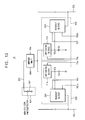
- FIG. 11 is a block diagram illustrating a unit pixel of a three-dimensional image sensor according to example embodiments.
- FIG. 12 is a circuit diagram illustrating an example of the unit pixel of FIG. 11 .
- FIG. 13 is a block diagram illustrating a unit pixel of a three-dimensional image sensor according to example embodiments.
- FIG. 14 is a circuit diagram illustrating an example of the unit pixel of FIG. 13 .
- FIG. 15 is a cross-sectional view of a unit pixel according to example embodiments.
- FIG. 16 is a diagram for describing quantum efficiency of non-silicon material.
- FIG. 17 is a diagram for describing bandgap energy of germanium compound.
- FIG. 18 is a block diagram illustrating a three-dimensional image sensor according to example embodiments.
- FIG. 19 is a diagram for describing an example operation of the unit pixel of FIG. 13 .
- FIG. 20 illustrates a block diagram of an example embodiment of a computer system including a three-dimensional image sensor.
- FIG. 21 illustrates a block diagram of an example embodiment of an interface employable in the computing system of FIG. 20 .
- FIG. 1 is a block diagram illustrating a unit pixel of a three-dimensional image sensor according to example embodiments.
- a unit pixel 10 may include a non-silicon photodetector 100 and at least one readout circuit 200 .
- FIG. 1 illustrates a non-limiting example such that the unit pixel 10 includes one readout circuit 200 .
- the unit pixel 10 may include two or more readout circuits.
- each unit pixel of the three-dimensional image sensor may include four readout circuits.
- the four readout circuits may generate four sensing signals, in response to four demodulation signals having phase difference of 90 degrees, respectively.
- the non-silicon photodetector 100 may be formed at a silicon substrate and include at least one of non-silicon materials to generate photocharge in response to incident light.
- the non-silicon materials may be germanium, silicon germanium compound, indium gallium arsenide, amorphous silicon germanium compound, black silicon germanium compound, porous silicon germanium compound, germanium antimony telluride, indium gallium antimonide, indium arsenide, mercury cadmium telluride, silicide, transition metal silicide, selenide, telluride, sulfide, etc.
- the non-silicon material may be silicon germanium compound Si (1-x) Ge (x) that includes germanium and silicon of x:(1-x) ratio.
- the non-silicon material may be indium gallium arsenide In (x) Ga (1-x) As that includes indium and gallium of x:(1-x) ratio.
- the other compounds having various elements of various ratios may be used to form the non-silicon photodetector 100 .
- Such non-silicon materials may have higher quantum efficiency, with respect to infrared light or light having a wavelength between 800 nm and 1400 nm than silicon materials.
- the non-silicon materials may be silicon arsenic telluride SiAsTe, silicon antimony telluride SiSbTe, silicon antimony selenide SiAsSe, germanium phosphorus selenide GePSe, germanium arsenic selenide GeAsSe, germanium arsenic telluride GeAsTe, germanium arsenic sulfide GeAsS, germanium antimony telluride GeSbTe, germanium antimony selenide GeSbSe, germanium antimony sulfide GeSbS, germanium bismuth selenide GeBiSe, germanium bismuth telluride GeBiTe, tin bismuth telluride, SnBiTe, tin bismuth selenide SnBiSe, tin antimony selenide SnSbSe, tin antimony telluride, SnSbTe, tin arsenic telluride SnAsTe, silicon
- the non-silicon photodetector 100 may include N-type non-silicon material at the P-type silicon substrate to form a PN diode.
- the non-silicon photodetector 100 may generate photocharge in response to incident light.
- the non-silicon photodetector may include a photo transistor, a photo gate, a pinned photo diode, etc.
- the incident light may include infrared light or light having a wavelength between 800 nm and 1400 nm.
- the incident light may be modulated light that has periodically-varying intensity.
- the non-silicon photodetector 100 may provide the generated photocharge to the readout circuit 200 through a conduction path 300 .
- the non-silicon photodetector 100 may be coupled to a low power voltage or a ground voltage VSS through a conduction path 190 .
- the readout circuit 200 may be formed at the silicon substrate.
- the readout circuit 200 may be configured to output a sensing signal based on the photocharge, where the sensing signal is used for generating depth information or distance information.
- the non-silicon photodetector 100 may be formed at a recess in the silicon substrate where the recess is adjacent to the readout circuit.
- the non-silicon photodetector 100 may also be formed on the readout circuit 200 .
- the readout circuit 200 may include a switching block 210 , a readout block 220 and a capacitor Ca.
- the switching block 210 may provide the charge from the non-silicon photodetector 100 to the capacitor Ca in synchronization with a demodulation signal TXa.
- the demodulation signal TXa may have a voltage level changing with the time period of the incident light.
- the demodulation signal TXa may have a frequency between 20 MHz and 60 MHz.
- the capacitor Ca may collect the charge provided through the switching block 210 .
- the capacitor Ca may include a first electrode, coupled to the low power voltage VSS, and a second electrode, coupled to the switching block 210 and the readout block 220 .
- the readout block 220 may output the sensing signal to a column line CL in response to a selection signal SELa where the sensing signal corresponds to a voltage VCa of the capacitor Ca, i.e., a voltage at the second electrode of the capacitor Ca.
- the readout block 220 may reset the voltage VCa of the capacitor Ca in response to a reset signal RST.
- the unit pixel 10 may operate in an integration mode, a readout mode and a reset mode.
- the readout circuit 200 may collect the charge from the non-silicon photodetector 100 in the capacitor Ca in response to the demodulation signal TXa.
- the readout circuit 200 may amplify the voltage VCa of the capacitor Ca and output the amplified voltage to the column line CL in response to the selection signal SELa.
- the readout circuit 200 may apply a reset voltage to the capacitor Ca in response to the reset signal RST. The reset voltage initializes the voltage VCa of the capacitor Ca.
- the readout circuit 200 may amplify the initialized voltage VCa of the capacitor Ca and output the amplified voltage to the column line CL in response to the selection signal SELa.
- the demodulation signal TXa may be deactivated while the readout circuit 200 senses the voltage VCa of the capacitor Ca.
- devices of sensing a depth may include a stereo image sensor, a time-of-flight (TOF) depth sensor, etc.
- the TOF depth sensor is in the three-dimension image sensor to obtain depth information, in addition to color image information.
- the three-dimensional TOF image sensor measures the distance to the object using infrared light or near-infrared light.
- the three-dimensional TOF image sensor using a silicon photodetector has relatively low quantum efficiency due to the low absorption coefficient of silicon with respect to the infrared light.
- the silicon material has the quantum efficiency of about 10% with respect to the infrared light.
- the silicon material has the quantum efficiency of about 60% with respect to the visible light.
- the unit pixel or the depth pixel, for measuring the depth information has relatively large occupation area to secure sufficient signal-to-noise ratio (SNR).
- SNR signal-to-noise ratio
- the unit pixel 10 of the three-dimensional image sensor includes the non-silicon photodetector 100 having the quantum efficiency with respect to the infrared light than the silicon photodetector.
- the unit pixel 10 may provide enhanced quality of image with the reduced occupation area and may increase the resolution of the three-dimensional image sensor.
- FIG. 2 is a block diagram illustrating an example of a readout block in the unit pixel of FIG. 1 .
- a readout block 220 may include a first switch 2201 , an amplifier 2202 and a second switch 2203 .
- the first switch 2201 may apply a reset voltage VDD to a capacitor Ca in response to a reset signal RST.
- the reset voltage initializes a voltage VCa of the capacitor Ca.
- the first switch 2201 may charge the capacitor CA periodically in response to the reset signal RST to perform correlated double sampling (CDS).
- the amplifier 2202 may amplify the voltage VCa of the capacitor Ca and output the amplified voltage.
- the amplifier 2202 may be implemented with one transistor that operates in an active mode or in a linear operation mode.
- the amplifier 2202 may operate as a source follower buffer transistor to amplify the voltage VCa of the capacitor Ca.
- the second switch 2203 may transfer the output of the amplifier 2202 to a column line CL in response to a selection signal SELa.
- the first and second switches 2201 and 2203 may include transistors.
- FIG. 3 is a circuit diagram illustrating an example of the unit pixel of FIG. 1 .
- a unit pixel 11 may include a non-silicon photodetector 101 and at least one readout circuit 201 .
- the non-silicon photodetector 101 may be formed at a silicon substrate and include at least one of non-silicon materials to generate photocharge in response to incident light.
- the non-silicon photodetector 101 may provide the photocharge to the readout circuit 201 through a conduction path 301 .
- the non-silicon photodetector 101 may be coupled to a low power voltage or a ground voltage VSS through a conduction path 191 .
- the readout circuit 201 may include a switching block 211 , a readout block 221 and a capacitor Ca.
- the switching block 211 may include a first transistor T 1 that is coupled between the capacitor Ca and the non-silicon photodetector 101 .
- the first transistor T 1 may receive a demodulation signal TXa through a control electrode, i.e., a gate electrode, and provide the charge from the non-silicon photodetector 101 to the capacitor Ca in synchronization with the demodulation signal TXa.
- the demodulation signal TXa may have a voltage level changing with the time period of the incident light.
- the capacitor Ca may collect the charge provided through the switching block 211 .
- the capacitor Ca may include a first electrode coupled to the low power voltage VSS and a second electrode coupled to the switching block 211 and the readout block 221 .
- the readout block 221 may include a second transistor T 2 , a third transistor T 3 , and a fourth transistor T 4 .
- the second transistor T 2 may be coupled between the second electrode of the capacitor Ca and a reset voltage.
- the reset voltage may be a high power voltage VDD.
- the second transistor T 2 may apply the high power voltage VDD to the second electrode of the capacitor Ca in response to a reset signal RST.
- the second transistor T 2 may initialize the voltage VCa of the capacitor Ca to the high power voltage VDD in response to the reset signal RST.
- the third transistor T 3 may be coupled between the high power voltage VDD and the fourth transistor T 4
- the fourth transistor T 4 may be coupled between the third transistor T 3 and a column line CL.
- the third transistor T 3 may receive the voltage VCa of the capacitor Ca through a control electrode and output a current to the fourth transistor T 4 in response to the voltage VCa of the capacitor Ca.
- the fourth transistor T 4 may output a sensing signal to the column line CL in response to a selection signal SELa.
- the readout block 221 may output the sensing signal corresponding to the voltage VCa of the capacitor Ca to the column line CL in response to the selection signal SELa.
- FIG. 4 is a cross-sectional view of a unit pixel according to example embodiments.
- the unit pixel 10 of FIG. 1 may be formed at the silicon substrate 20 a .
- the non-silicon photodetector 100 of FIG. 1 may be formed in a non-silicon photodetector region 100 a and the readout circuit 200 of FIG. 1 may be formed in a readout circuit region 200 a .
- the non-silicon photodetector region 100 a and the readout circuit region 200 a may be electrically connected through a conduction path 300 a.
- the readout circuit region 200 a may be formed near an upper surface of the silicon substrate 20 a and the non-silicon photodetector region 100 a may be formed at a recess in the silicon substrate 20 a where the recess is adjacent to the readout circuit region 200 a .
- the non-silicon photodetector region 100 a may include an insulation portion 120 a and a non-silicon material portion 110 a surrounded by the insulation portion 120 a .
- the non-silicon material portion 110 a may be formed through a growth process or a deposition process to fill the recess with the above-mentioned non-silicon material.
- the bottom surface 190 a of the non-silicon material portion 110 a may contact the silicon substrate 20 a so that the non-silicon material portions of a plurality of unit pixels may be commonly connected with the silicon substrate 20 a.
- a horizontal cross-section of the non-silicon photodetector or the non-silicon material portion 110 a may be decreased gradually along a depth of the horizontal cross-section.
- the insulation portion 120 a may be formed like a truncated funnel and the non-silicon material may fill the inner space of the funnel-like insulation portion 120 a .
- an upper surface of the non-silicon photodetector may have a largest area and a bottom surface of the non-silicon photodetector may have a smallest area.
- the silicon substrate 20 a may include a P-type epitaxial substrate that is formed on a P-type bulk silicon substrate through an epitaxial process.
- the P-type epitaxial substrate may be formed using a silicon source gas to have the same crystalline structure with the P-type bulk silicon substrate.
- the silicon source gas may include at least one of silane, dichlorosilane (DCS), trichlorosilane (TCS) and hexachlorosilane (DCS).
- FIGS. 5 and 6 are cross-sectional views illustrating examples of the unit pixel of FIG. 4 .
- the unit pixel 10 of FIG. 1 may be formed at the silicon substrate 21 a .
- the non-silicon photodetector 100 of FIG. 1 may be formed in a non-silicon photodetector region 101 a and the readout circuit 200 of FIG. 1 may be formed adjacent to the photodetector region 101 a .
- the first transistor T 1 in FIG. 3 may be formed in the transistor region T 1 a .
- the non-silicon photodetector region 101 a and the first transistor T 1 may be electrically connected through a conduction path 301 a .
- the conduction path 301 a may include a wire, in a metal layer over the silicon substrate 21 a , and vertical contacts, connecting the wire and the upper surface of the silicon substrate 21 a.
- the transistor region T 1 a may be formed near the upper surface of the silicon substrate 21 a .
- the transistor region T 1 a may include N-type silicon regions and a gate electrode TXa.
- the non-silicon photodetector region 101 a may be formed at a recess in the silicon substrate 21 a .
- the recess is adjacent to the readout circuit region.
- the readout circuit region includes the transistor region T 1 a .
- the non-silicon photodetector region 101 a may include an insulation portion 121 a and a non-silicon material portion 111 a surrounded by the insulation portion 121 a .
- the bottom surface 191 a of the non-silicon material portion 111 a may contact with the silicon substrate 21 a so that the non-silicon material portions of a plurality of unit pixels may be commonly connected with the silicon substrate 21 a.
- a filter 180 a may be formed over the non-silicon photodetector region 101 a .
- the filter 180 a may pass light L 2 having a wavelength of a predetermined range among the incident light L 1 .
- the filter 180 a may be a band pass filter that passes infrared light having the wavelength between 800 nm and 1400 nm or a band pass filter that passes near-infrared light having the wavelength between 800 nm and 900 nm.
- the non-silicon material portion 111 a of FIG. 5 may include P-type germanium 131 a and N-type germanium 141 a .
- the P-type germanium 131 a may be formed on the P-type silicon and the N-type germanium 141 a may be formed on the P-type germanium 131 a .
- the P-type germanium 131 a and the N-type germanium 141 a may form a PN junction.
- the non-silicon photodetector 100 of FIG. 1 may form a PN junction diode.
- the non-silicon material portion 111 a may include intrinsic germanium.
- the non-silicon photodetector 100 may be a photoconductor including the intrinsic germanium.
- the non-silicon material portion 111 a may include intrinsic germanium and P-type germanium formed on a doped region including N-type silicon.
- the doped region and the non-silicon photodetector 100 may form a PIN junction diode.
- FIG. 7 is a cross-sectional view of a unit pixel according to example embodiments.
- the unit pixel 10 of FIG. 1 may be formed at the silicon substrate 20 b as illustrated in FIG. 7 .
- the non-silicon photodetector 100 of FIG. 1 may be formed in a non-silicon photodetector region 100 b and the readout circuit 200 of FIG. 1 may be formed in a readout circuit region 200 b .
- the non-silicon photodetector region 100 b and the readout circuit region 200 b may be electrically connected through a conduction path 300 b.
- the readout circuit region 200 b may be formed near an upper surface of the silicon substrate 20 b and the non-silicon photodetector region 100 b may be formed on the readout circuit region 200 b .
- the non-silicon photodetector region 100 b may include a non-silicon material portion 110 b formed in an insulation material layer 30 b .
- the non-silicon photodetector region 100 b may be electrically connected to the non-silicon photodetector regions of the neighboring unit pixels through conduction paths 190 b .
- a planarization process may be performed on the non-silicon material portion 110 b and the insulation material layer 30 b before forming the conduction paths 190 b.
- FIGS. 8 , 9 and 10 are cross-sectional views illustrating examples of the unit pixel of FIG. 7 .
- the unit pixel 10 of FIG. 1 may be formed at the silicon substrate 21 b .
- the non-silicon photodetector 100 of FIG. 1 may be formed in a non-silicon photodetector region 101 b and the readout circuit 200 of FIG. 1 may be formed under the photodetector region 101 b .
- the first transistor T 1 in FIG. 3 may be formed in the transistor region T 1 b .
- the non-silicon photodetector region 101 b may include a non-silicon material region 111 b formed in an insulation material layer 30 b .
- the non-silicon material region 111 b formed in an insulation material layer 31 b .
- the first transistor T 1 may be electrically connected to the non-silicon material region 111 b through a bottom surface of the non-silicon material region 111 b.
- the transistor region T 1 b may be formed near the upper surface of the silicon substrate 21 b .
- the transistor region T 1 b may include N-type silicon regions and a gate electrode TXa.
- the non-silicon material region 111 b may be formed on a doped region including N-type silicon. The bottom surface of the non-silicon material portion 111 b may contact with the doped region forming the transistor T 1 .
- a filter 181 b may be formed over the non-silicon photodetector region 101 b .
- the filter 181 b may pass light L 2 having a wavelength of a predetermined range among the incident light L 1 .
- the filter 181 b may be a band pass filter that passes infrared light having the wavelength between 800 nm and 1400 nm or a band pass filter that passes near-infrared light having the wavelength between 800 nm and 900 nm.
- the non-silicon material portion 111 b of FIG. 8 may include P-type germanium 131 b and N-type germanium 141 b .
- the N-type germanium 141 b may be formed on the doped region including N-type silicon and the P-type germanium 131 b may be formed on the N-type germanium 141 b .
- the P-type germanium 131 b and the N-type germanium 141 b may form a PN junction.
- the non-silicon photodetector 100 of FIG. 1 may form a PN junction diode.
- the non-silicon material portion 111 b of FIG. 8 may include intrinsic germanium 161 b and P-type germanium 151 b .
- the intrinsic germanium 161 b may be formed on the doped region including N-type silicon and the P-type germanium 151 b may be formed in the upper portions of the intrinsic germanium 161 b .
- the P-type germanium 151 b , the intrinsic germanium 161 b , and the doped region may form a PIN junction.
- the doped region and the non-silicon photodetector 100 of FIG. 1 may form a PIN junction diode.
- the P-type germanium 151 b may be omitted in the non-silicon photodetector region 101 b of FIG. 10 .
- the non-silicon photodetector 100 of FIG. 1 may be a photoconductor including intrinsic germanium 161 b.
- FIG. 11 is a block diagram illustrating a unit pixel of a three-dimensional image sensor according to example embodiments.
- a unit pixel 12 may include a non-silicon photodetector 102 , a first readout circuit 202 and a second readout circuit 402 .
- FIG. 11 illustrates a non-limiting example that the unit pixel 12 includes the two readout circuits 202 and 402 , but the unit pixel 12 may include three or more readout circuits.
- the readout circuits 202 and 402 may be electrically connected to the non-silicon photodetector 102 through a conduction path 302 .
- the non-silicon photodetector 102 may be formed at a silicon substrate and include at least one of non-silicon materials to generate photocharge in response to incident light.
- the non-silicon materials may be germanium, silicon germanium compound, indium gallium arsenide, amorphous silicon germanium compound, black silicon germanium compound, porous silicon germanium compound, germanium antimony telluride, indium gallium antimonide, indium arsenide, mercury cadmium telluride, silicide, transition metal silicide, selenide, telluride, sulfide, etc.
- the non-silicon material may be silicon germanium compound Si (1-x) Ge (x) that includes germanium and silicon of x:(1-x) ratio.
- the non-silicon material may be indium gallium arsenide In (x) Ga (1-x) . As that includes indium and gallium of x:(1-x) ratio.
- the other compounds having various elements of various ratios may be used to form the non-silicon photodetector 102 .
- Such non-silicon materials may have higher quantum efficiency, with respect to infrared light or light having a wavelength between 800 nm and 1400 nm than silicon materials.
- the non-silicon materials may be silicon arsenic telluride SiAsTe, silicon antimony telluride SiSbTe, silicon antimony selenide SiAsSe, germanium phosphorus selenide GePSe, germanium arsenic selenide GeAsSe, germanium arsenic telluride GeAsTe, germanium arsenic sulfide GeAsS, germanium antimony telluride GeSbTe, germanium antimony selenide GeSbSe, germanium antimony sulfide GeSbS, germanium bismuth selenide GeBiSe, germanium bismuth telluride GeBiTe, tin bismuth telluride, SnBiTe, tin bismuth selenide SnBiSe, tin antimony selenide SnSbSe, tin antimony telluride, SnSbTe, tin arsenic telluride SnAsTe, silicon
- the non-silicon photodetector 102 may generate a photocharge in response to incident light.
- the incident light may be infrared light or light having a wavelength between 800 nm and 1400 nm.
- the incident light may be modulated light that has periodically-varying intensity.
- the non-silicon photodetector 102 may provide the generated photocharge to the readout circuits 202 and 204 through the conduction path 302 .
- the non-silicon photodetector 102 may be coupled to a low power voltage or a ground voltage VSS through a conduction path 192 .
- the first and second readout circuits 202 and 402 may be formed at the silicon substrate and the first and second readout circuits 202 and 402 may be configured to output respective sensing signals based on the photocharge generated in the non-silicon photodetector 102 .
- the sensing signals are used for generating depth information or distance information.
- the non-silicon photodetector 102 may be formed at a recess in the silicon substrate where the recess is adjacent to the readout circuits 202 and 402 .
- the non-silicon photodetector 102 may also be formed on the readout circuits 202 and 402 .
- the first readout circuit 202 may include a first switching block 212 , a first readout block 222 , and a first capacitor Ca.
- the first switching block 212 may provide the charge from the non-silicon photodetector 102 to the first capacitor Ca in synchronization with a first demodulation signal TXa.
- the first demodulation signal TXa may have a voltage level changing with the time period of the incident light.
- the first demodulation signal TXa may have a frequency between 20 MHz and 60 MHz.
- the first capacitor Ca may collect the charge provided through the first switching block 212 in response to the first demodulation signal TXa.
- the first capacitor Ca may include a first electrode coupled to the low power voltage VSS and a second electrode coupled to the first switching block 212 and the first readout block 222 .
- the first readout block 222 may output a first sensing signal to a first column line OCL in response to a first selection signal SELa.
- the first sensing signal corresponds to a voltage VCa of the first capacitor Ca, i.e., a voltage at the second electrode of the first capacitor Ca.
- the first column line OCL may be an odd-numbered line of a plurality of column lines of a pixel array.
- the first readout block 222 may initialize the voltage VCa of the first capacitor Ca in response to a reset signal RST.
- the second readout circuit 402 may include a second switching block 412 , a second readout block 422 , and a second capacitor Cb.
- the second switching block 412 may provide the charge from the non-silicon photodetector 102 to the second capacitor Cb in synchronization with a second demodulation signal TXb.
- the second demodulation signal TXb may have a voltage level changing with the time period of the incident light but a different phase from the first demodulation signal TXa.
- the second demodulation signal TXb may have a frequency between 20 MHz and 60 MHz.
- the phase difference between the first and second demodulation signals TXa and TXb may be 180 degrees.
- the second capacitor Cb may collect the charge provided through the second switching block 412 in response to the second demodulation signal TXb.
- the second capacitor Cb may include a first electrode coupled to the low power voltage VSS and a second electrode coupled to the second switching block 412 and the second readout block 422 .
- the second readout block 422 may output a second sensing signal to a second column line ECL in response to a second selection signal SELb.
- the second sensing signal corresponds to a voltage VCb of the second capacitor Cb, i.e., a voltage at the second electrode of the second capacitor Cb.
- the second column line ECL may be an even-numbered line of the column lines of the pixel array.
- the second readout block 422 may initialize the voltage VCb of the second capacitor Cb in response to the reset signal RST.
- the unit pixel 12 may operate in an integration mode, a readout mode, and a reset mode.
- the first readout circuit 202 may collect the charge from the non-silicon photodetector 102 in the first capacitor CA in response to the first demodulation signal TXa and the second readout circuit 402 may collect the charge from the non-silicon photodetector 102 in the second capacitor Cb in response to the second demodulation signal TXb.
- the first readout circuit 202 may amplify the voltage VCa of the first capacitor Ca and output the amplified voltage to the first column line OCL in response to the first selection signal SELa.
- the second readout circuit 402 may amplify the voltage VCb of the second capacitor Cb and output the amplified voltage to the second column line ECL in response to the second selection signal SELb.
- the first and second readout circuit 202 and 402 may apply a reset voltage to the first and second capacitors Ca and Cb in response to the reset signal RST.
- the reset voltage initializes the voltages VCa and VCb of the first and second capacitors Ca and Cb.
- the first and second readout circuits 202 and 402 may amplify the initialized voltages VCa and VCb of the first and second capacitors Ca and Cb and output the amplified voltages to the first and second column lines OCL and ECL in response to the first and second selection signals SELa and SELb, respectively.
- the first and second demodulation signals TXa and TXb may be deactivated while the first and second readout circuits 202 and 402 sense the voltages VCa and VCb of the first and second capacitors Ca and Cb.
- the first demodulation signal TXa and the second demodulation signal TXb may have a phase difference of 180 degrees.
- the first and second demodulation signals TXa and TXb may have complementary signal levels.
- the second demodulation signals TXb may be an inversion signal of the first demodulation signal TXa.
- the photocharge generated in the non-silicon photodetector 102 may be alternatively provided to the first and second capacitors Ca and Cb per half cyclic period of the demodulation signals TXa and TXb.
- the unit pixel 12 of the three-dimensional image sensor includes the non-silicon photodetector 102 having the quantum efficiency with respect to the infrared light, rather than the silicon photodetector.
- the unit pixel 12 may provide enhanced quality of image with the reduced occupation area and may increase the resolution of the three-dimensional image sensor.
- FIG. 12 is a circuit diagram illustrating an example of the unit pixel of FIG. 11 .
- a unit pixel 13 may include a non-silicon photodetector 103 , a first readout circuit 203 , and a second readout circuit 403 .
- the first readout circuit 203 may include a first switching block 213 , a first readout block 223 , and a first capacitor Ca.
- the second readout circuit 403 may include a second switching block 413 , a second readout block 423 , and a second capacitor Cb.
- the first switching block 213 may include a first transistor T 11 that is coupled between the first capacitor Ca and the non-silicon photodetector 103 .
- the first transistor T 11 may receive a first demodulation signal TXa through a control electrode, i.e., a gate electrode, and provides the charge from the non-silicon photodetector 103 to the first capacitor Ca in synchronization with the first demodulation signal TXa.
- the first demodulation signal TXa may have a voltage level changing with the time period of the incident light.
- the first capacitor Ca may collect the charge provided through the first switching block 213 .
- the first capacitor Ca may include a first electrode, coupled to the low power voltage VSS, and a second electrode, coupled to the first switching block 213 and the first readout block 223 .
- the first readout block 223 may include a second transistor T 21 , a third transistor T 31 , and a fourth transistor T 41 .
- the second transistor T 21 may be coupled between the second electrode of the first capacitor Ca and a reset voltage.
- the reset voltage may be a high power voltage VDD.
- the second transistor T 21 may apply the high power voltage VDD to the second electrode of the first capacitor Ca in response to a reset signal RST.
- the second transistor T 21 may initialize the voltage VCa of the first capacitor Ca to the high power voltage VDD in response to the reset signal RST.
- the third transistor T 31 may be coupled between the high power voltage VDD and the fourth transistor T 41 .
- the fourth transistor T 41 may be coupled between the third transistor T 31 and a first column line OCL.
- the third transistor T 31 may receive the voltage VCa of the first capacitor Ca through a control electrode and output a current to the fourth transistor T 41 in response to the voltage VCa of the first capacitor Ca.
- the fourth transistor T 41 may output a first sensing signal to the first column line OCL in response to a first selection signal SELa. Therefore, the first readout block 223 may output the first sensing signal corresponding to the voltage VCa of the first capacitor Ca to the first column line OCL in response to the first selection signal SELa.
- the configuration and operation of the second readout circuit 403 is similar to the first readout circuit 203 . Repeated descriptions are omitted.
- the second switching block 413 provides the charge from the non-silicon photodetector 103 to the second capacitor Cb in synchronization with the second demodulation signal TXb, instead of the first demodulation signal TXa.
- the first demodulation signal TXa and the second demodulation signal TXb may have a phase difference of 180 degrees as illustrated in FIG. 19 .
- the second demodulation signals TXb may be an inversion signal of the first demodulation signal TXa.
- the photocharge generated in the non-silicon photodetector 102 may be alternatively provided to the first and second capacitors Ca and Cb per half cyclic period of the demodulation signals TXa and TXb.
- the photocharge, corresponding to one half of the cyclic period may be collected in the first capacitor Ca and the photocharge, corresponding to the other half of the cyclic period, may be collected in the second capacitor Cb.
- FIG. 13 is a block diagram illustrating a unit pixel of a three-dimensional image sensor according to example embodiments.
- a unit pixel 14 may include a non-silicon photodetector 104 , a first readout circuit 204 , a second readout circuit 404 , and a buffer unit 504 .
- the readout circuits 204 and 404 may be electrically connected to the non-silicon photodetector 104 through a conduction path 304 and the buffer unit 504 .
- the configuration and operation of the unit pixel 14 of FIG. 13 are similar to those of the unit pixels 12 and 13 of FIGS. 11 and 12 except the buffer unit 504 . Repeated descriptions may be omitted.
- the buffer unit 504 may be coupled between the non-silicon photodetector 104 and the readout circuits 204 and 404 .
- the buffer unit 504 may be turned on and off in response to a buffer control signal Vbb.
- the buffer unit 504 may transfer the charge from the non-silicon photodetector 104 to the readout circuits 204 and 404 in response to the buffer control signal Vbb.
- the buffer unit 504 may maintain a substantially constant bias across the non-silicon photodetector 104 .
- the charge transfer between the non-silicon photodetector 504 and the readout circuits 204 and 404 may be buffered by the buffer unit 504 so that the non-silicon photodetector 104 may be isolated from capacitive interference due to the switching operations of the switching blocks 214 and 414 .
- the unit pixel 14 may operate in an integration mode, a readout mode, and a reset mode.
- the buffer control signal Vbb may be activated in the integration mode to turn on the buffer unit 504 .
- the first readout circuit 204 may collect the charge from the non-silicon photodetector 104 in the first capacitor CA in response to the first demodulation signal TXa
- the second readout circuit 404 may collect the charge from the non-silicon photodetector 104 in the second capacitor Cb in response to the second demodulation signal TXb.
- the first readout circuit 204 may amplify the voltage VCa of the first capacitor Ca and output the amplified voltage, i.e., the first sensing signal to the first column line OCL in response to the first selection signal SELa
- the second readout circuit 404 may amplify the voltage VCb of the second capacitor Cb and output the amplified voltage, i.e., the second sensing signal to the second column line ECL in response to the second selection signal SELb.
- the first and second readout circuit 204 and 404 may apply a reset voltage to the first and second capacitors Ca and Cb in response to the reset signal RST to initialize the voltages VCa and VCb of the first and second capacitors Ca and Cb.
- the first and second readout circuits 202 and 402 may amplify the initialize voltages VCa and VCb of the first and second capacitors Ca and Cb and output the amplified voltages to the first and second column lines OCL and ECL in response to the first and second selection signals SELa and SELb, respectively.
- the first and second demodulation signals TXa and TXb may be deactivated while the first and second readout circuits 204 and 404 sense the voltages VCa and VCb of the first and second capacitors Ca and Cb.
- FIG. 14 is a circuit diagram illustrating an example of the unit pixel of FIG. 13 .
- a unit pixel 15 may include a non-silicon photodetector 105 , a first readout circuit 205 , a second readout circuit 405 , and a buffer unit 505 .
- the configuration and operation of the unit pixel 15 of FIG. 14 are similar to those of the unit pixels 12 , 13 and 14 of FIGS. 11 , 12 and 13 . Repeated descriptions may be omitted.
- the buffer unit 505 may include a buffer transistor T 5 .
- the buffer transistor T 5 may receive the buffer control signal Vbb through a control electrode, i.e., a gate electrode, and control the electrical connection between the non-silicon photodetector 105 and the readout circuits 205 and 405 in response to the buffer control signal Vbb.
- the buffer transistor T 5 of the buffer unit 505 may maintain substantially constant bias across the non-silicon photodetector 505 .
- the charge transfer between the non-silicon photodetector 505 and the readout circuits 205 and 405 may be buffered by the buffer transistor T 5 so that the non-silicon photodetector 105 may be isolated from capacitive interference due to the switching operations of the switching blocks 215 and 415 .
- the output capacitance of the non-silicon photodetector 105 may be kept small through merging the buffer transistor T 5 between the non-silicon photodetector 105 and the readout circuits 205 and 405 .
- FIG. 15 is a cross-sectional view of a unit pixel according to example embodiments.
- the unit pixel 15 of FIG. 14 may be formed at the silicon substrate 25 a .
- the non-silicon photodetector 105 of FIG. 14 may be formed in a non-silicon photodetector region 105 a and the readout circuits 205 and 405 of FIG. 14 may be formed adjacent to the photodetector region 105 a .
- the buffer transistor T 5 of the buffer unit 505 in FIG. 14 may be formed in the buffer transistor region T 5 a and the switching transistor T 11 of the first switching block 215 may be formed in the switching transistor region T 11 a .
- the non-silicon photodetector region 105 a and the buffer transistor T 5 may be electrically connected through a conduction path 305 a .
- the conduction path 305 a may include a wire in a metal layer over the silicon substrate 25 a and vertical contacts connecting the wire and the upper surface of the silicon substrate 25 a.
- the buffer transistor region T 5 a and the switching transistor region T 11 a may be formed near the upper surface of the silicon substrate 25 a.
- the buffer transistor region T 5 a may include N-type silicon regions and a gate electrode Vbb.
- the switching transistor region T 11 a may include N-type silicon regions and a gate electrode TXa.
- the non-silicon photodetector region 105 a may be formed at a recess in the silicon substrate 25 a where the recess is adjacent to the buffer transistor region T 5 a .
- the non-silicon photodetector region 105 a may include an insulation portion 125 a and a non-silicon material portion surrounded by the insulation portion 125 a .
- the non-silicon material portion may include P-type germanium 135 a and N-type germanium 145 a formed on the P-type germanium 135 a . In other words, the P-type germanium 135 a and the N-type germanium 145 a may form a PN junction.
- the non-silicon photodetector 105 of FIG. 14 may form a PN junction diode.
- FIG. 16 is a diagram for describing quantum efficiency of non-silicon material.
- the horizontal reference axis represents a wavelength ( ⁇ m) of incident light to photosensing materials such as Ge, Si GaAs, In (0.7) Ga (0.3) As (0.67) P (0.86) , In (0.53) Ga (0.47) .
- As and the vertical reference axis represents a absorption coefficient (1/cm) or a penetration depth ( ⁇ m).
- germanium Ge has the higher absorption coefficient or the lower penetration depth with respect to infrared light than silicon Si. With respect to near-infrared light having the wavelength of about 800 nm, germanium Ge has the absorption coefficient about fifty times higher than the absorption coefficient of silicon Si. The higher absorption coefficient corresponds to the higher quantum efficiency.
- the non-silicon material, i.e., germanium may be used to implement a photodetector having high quantum efficiency.
- FIG. 17 is a diagram for describing bandgap energy of germanium compound.
- the horizontal reference axis represents a fraction (x) of germanium and the vertical reference axis represents a minimum bandgap energy (eV) at the absolute temperature 90 K.
- the bandgap energy is decreased as the germanium fraction is increased in the various strained or unstrained germanium compounds. Even though the germanium fraction is low in the germanium compounds, the bandgap energy may be decreased to the meaningful level.
- the non-silicon material forming the non-silicon photodetector according to example embodiments may be silicon germanium, strained silicon on silicon germanium, strained silicon germanium on silicon germanium, or strained silicon germanium on silicon.
- FIG. 18 is a block diagram illustrating a three-dimensional image sensor according to example embodiments.
- a three-dimensional image sensor 700 may include a pixel array 710 , an analog-to-digital conversion (ADC) circuit 720 , a row scanning circuit 730 , a column scanning circuit 740 , a control circuit 750 , a light source module 770 and an image signal processor (ISP) 800 .
- ADC analog-to-digital conversion
- ISP image signal processor
- the pixel array 710 may include a plurality of unit pixels, i.e., depth pixels that convert incident light L 1 to electric signals where the incident light includes a transmission light ML reflected by an object 30 .
- the depth pixels may provide the electric signals representing depth information or distance information to obtain a distance to the object 30 .
- each of the depth pixels in the pixel array 710 may include the non-silicon photodetector 100 and at least one readout circuit 200 as illustrated in FIG. 1 .
- the non-silicon photodetector 100 may be formed at a silicon substrate and include at least one of non-silicon materials to generate photocharge in response to the incident light L 1 .
- the non-silicon materials may be germanium, silicon germanium compound, indium gallium arsenide, amorphous silicon germanium compound, black silicon germanium compound, porous silicon germanium compound, germanium antimony telluride, indium gallium antimonide, indium arsenide, mercury cadmium telluride, silicide, transition metal silicide, selenide, telluride, sulfide, etc.
- the non-silicon material may be silicon germanium compound Si (1-x) Ge (x) that includes germanium and silicon of x:(1-x) ratio.
- the non-silicon material may be indium gallium arsenide In (x) Ga (1-x) As that includes indium and gallium of x:(1-x) ratio.
- the other compounds having various elements of various ratios may be used to form the non-silicon photodetector 100 .
- Such non-silicon materials may have higher quantum efficiency with respect to infrared light or light having a wavelength between 800 nm and 1400 nm than silicon materials.
- the non-silicon photodetector 100 may be formed at the silicon substrate using photosensitive semiconductor quantum dots.
- the incident light L 1 may include infrared light or light having a wavelength between 800 nm and 1400 nm.
- the incident light L 1 may be the modulated light that has periodically-varying intensity.
- the non-silicon photodetector 100 may provide the generated photocharge to the readout circuit 200 through a conduction path 300 .
- the non-silicon photodetector 100 may be coupled to a low power voltage or a ground voltage VSS through a conduction path 190 .
- the readout circuit 200 may be formed at the silicon substrate and the readout circuit 200 may be configured to output the sensing signal based on the photocharge.
- the photocharge is where the sensing signal is used for generating depth information or distance information.
- the non-silicon photodetector 100 may be formed at a recess in the silicon substrate where the recess is adjacent to the readout circuit, or the non-silicon photodetector 100 may be formed on the readout circuit 200 .
- the readout circuit 200 may include the switching block 210 , the readout block 220 , and the capacitor Ca.
- the switching block 210 may provide the charge from the non-silicon photodetector 100 to the capacitor Ca in synchronization with the demodulation signal TXa.
- the demodulation signal TXa may have a voltage level changing with the time period of the incident light.
- the capacitor Ca may collect the charge provided through the switching block 210 in response to the demodulation signal TXa.
- the capacitor Ca may include the first electrode coupled to the low power voltage VSS and the second electrode coupled to the switching block 210 and the readout block 220 .
- the readout block 220 may output the sensing signal to the column line CL in response to the selection signal SELa where the sensing signal corresponds to the voltage VCa of the capacitor Ca, i.e., voltage at the second electrode of the capacitor Ca.
- the readout block 220 may initialize the voltage VCa of the capacitor Ca in response to the reset signal RST.
- the pixel array may further include a plurality of color pixels and the three-dimensional image sensor 700 may provide depth information and color image information.
- the color pixels may be formed at the silicon substrate between the depth pixels and the number ratio of the depth pixels and the color pixels may be changed variously.
- the color pixels may convert visible light to color image signals.
- the visible light may be included in the incident light.
- the color pixels may have higher quantum efficiency with respect to the visible light than the depth pixels.
- Color filters such as red filters, green filters and blue filters may be formed over the color pixels and infrared filters or near-infrared filters may be formed over the depth filters.
- the ADC circuit 720 may convert analog signals from the pixel array 710 to digital signals to provide first image signals LDI. According to example embodiments, the ADC circuit may perform column ADC that converts analog signals in parallel using a plurality of analog-to-digital converters respectively coupled to a plurality of column lines, or may perform single ADC that converts the analog signals in series using a single analog-to-digital converter.
- the ADC circuit 720 may include a correlated double sampling (CDS) unit for extracting an effective signal component (the valid voltage).
- the CDS unit may perform analog double sampling (ADS) that extracts the effective signal component based on an analog reset signal that represents a reset component and an analog data signal that represents a signal component.
- the CDS unit may perform digital double sampling (DDS) that converts the analog reset signal and the analog data signal into two digital signals to extract as the effective signal component a difference between the two digital signals.
- DDS digital double sampling
- the CDS unit may perform dual correlated double sampling that performs both of analog double sampling and digital double sampling.
- the row scanning circuit 730 may receive control signals from the control circuit 750 to control a row address of the pixel array 710 .
- the row scanning circuit 730 may include a row decoder configured to select a row line among a plurality of row lines of the pixel array 710 and a row driver configured to activate the selected row line.
- the column scanning circuit 740 may receive control signals from the control circuit 750 to control a column address of the pixel array 710 to provide the first image signals LDI to the image signal process 800 .
- the column scanning circuit 740 may sequentially select the analog-to-digital converters in the ADC circuit 720 to output the first image signals LDI.
- the column scanning circuit 740 may include a column decoder configured to select one of the analog-to-digital converters and a column driver configured to transfer the output of the selected analog-to-digital converter.
- the control circuit 750 may control the ADC circuit 720 , the row scanning circuit 730 , the column scanning circuit 740 , and the light source module 770 .
- the control circuit 750 may provide respective control signals, i.e., clock signals, timing control signals for operations of the ADC circuit 720 , the row scanning circuit 730 , the column scanning circuit 740 , and the light source module 770 .
- the control circuit 750 may include a control logic, a phased-locked loop, a timing control circuit, a communication interface circuit, etc.
- the light source module 770 may emit a modulated transmission light ML having a given, desired, or predetermined wavelength.
- the light source module 770 may emit infrared light or near-infrared light.
- the emitted light ML generated by the light source module 770 may be focused on the object 30 by a lens 772 .
- the light source module 770 may be controlled by the control signal from the control circuit 750 to output the modulated transmission light ML such that the intensity of the modulated transmission light ML periodically changes.
- the modulated transmission light ML may be a pulse wave, a sine wave, a cosine wave, etc.
- the light source module 770 may be implemented with a light source 771 , i.e., a light emitting diode (LED), a laser diode, etc.
- the control circuit 750 controls the light source module 770 to output the modulated transmission light ML having periodically-varying intensity.
- the modulated transmission light ML is reflected by the object 30 and the reflected light may be included in the incident light L 1 input to the pixels in the pixel array 710 .
- the pixels selected by the row scanning circuit 730 output the analog signals corresponding to the incident light L 1 .
- the ADC circuit 720 converts the analog signals to the digital signals and the column scanning circuit 740 sequentially select the digital signals to provide the first image signal LDI.
- the digital signal processor 800 may process the first image signal LDI to provide the depth information IND.
- the pixel array 710 may further include color pixels and the image signal processor 800 may the depth information and the color image information.
- the unit pixel or the depth pixel of the three-dimensional image sensor 700 may include the non-silicon photodetector having the higher quantum efficiency than the silicon photodetector.
- the unit pixel or the depth pixel may sense the infrared light with enhanced efficiency. Accordingly the three-dimensional image sensor 700 may provide an image of higher resolution, than the related art image sensor which only includes the silicon photodetector.
- FIG. 19 is a diagram for describing an example operation of the unit pixel of
- the three-dimensional image sensor 700 may emit the modulated transmission light ML having the intensity varying periodically.
- the three-dimensional image sensor 700 may turn on and off the light source 771 with a frequency of 10 through 200 MHz to generate the modulated transmission light ML.
- the modulated transmission light ML is reflected by the object 30 and returns to the three-dimensional image sensor 700 as the incident light L 1 .
- the incident light L 1 is delayed by the time-of-flight TOF with respect to the modulated transmission light ML.
- the TOF corresponds to the time interval t 2 -t 1 or t 4 -t 3 .
- the first demodulation signal TXa may have the phase equal to the phase of the modulated transmission light ML
- the second demodulation signal TXb may have the phase opposite to the phase of the modulated transmission light ML.
- the first and second demodulation signals TXa and TXb may have a phase difference of 180 degrees.
- the buffer control signal Vbb may be activated, for example, to a logic high level, to turn on the buffer unit 505 of FIG. 14 .
- a first charge P 2 of the photocharge P 1 generated in the non-silicon photodetector may be collected in the first capacitor Ca in response to the first demodulation signal TXa and a second charge P 3 of the photocharge P 1 may be collected in the second capacitor Cb in response to the second demodulation signal TXb.
- the activation voltage level of the demodulated signals TXa and TXb may be about 3V and the deactivation voltage level of demodulated signals TXa and TXb may be about 0V.
- the ratio of the first and second charges P 2 and P 3 may be changed depending on the TOF. As the TOF increases, the first charge P 2 collected by the first capacitor Ca may be decreased and the second charge P 3 collected by the second capacitor Cb may be increased. Thus, the three-dimensional image sensor 700 may calculate the TOF, i.e., the delay time of the incident light L 1 with respect to the modulated transmission light ML, by measuring the ratio of the charges respectively collected in the first and second capacitors Ca and Cb.
- the distance to the object 30 may be calculated based on the obtained TOF.
- the first switching block 215 may be turned on in response to the first demodulation signal TXa to collect the first charge P 2 in the first capacitor Ca and the second switching block 415 may be turned on in response to the second demodulation signal TXb to collect the second charge P 3 in the second capacitor C 2 .
- the three-dimensional image sensor 700 may sample the sensing signals corresponding to the charges respectively collected in the capacitors Ca and Cb.
- the reset signal RST is activated after the first sampling time TSS, the reset voltage or the high power voltage VDD is applied to the capacitors Ca and Cb to initialize the voltages VCa and VCb of the capacitors Ca and Cb.
- the three-dimensional image sensor 700 may sample the initialize signals corresponding to the reset states of the capacitors Ca and Cb.
- the sensing signals sampled at the time TSS and the initialized signals sampled at the time TRS may be used to perform the correlated double sampling.
- FIG. 19 illustrates a non-limiting example using a pulse signal as the modulated transmission light ML and the demodulation signals TXa and TXb.
- various periodic signals such as a sine signal, a cosine signal, etc., may be used as the modulated transmission light ML and the demodulation signals TXa and TXb.
- FIG. 20 illustrates a block diagram of an example embodiment of a computer system including a three-dimensional image sensor.
- a computing system 1000 may include a processor 1010 , a memory device 1020 , a storage device 1030 , an input/output device 1040 , a power supply 1050 , and a three-dimensional image sensor 700 .
- the computing system 1000 may further include ports that communicate with a video card, a sound card, a memory card, a universal serial bus (USB) device, or other electronic devices.
- USB universal serial bus
- the processor 1010 may perform various calculations or tasks. According to at least some example embodiments, the processor 1010 may be a microprocessor or a CPU. The processor 1010 may communicate with the memory device 1020 , the storage device 1030 , and the input/output device 1040 via an address bus, a control bus, and/or a data bus. In at least some example embodiments, the processor 1010 may be coupled to an extended bus, such as a peripheral component interconnection (PCI) bus.
- the memory device 1020 may store data for operating the computing system 1000 .
- the memory device 1020 may include volatile memory such as dynamic random access memory (DRAM), mobile DRAM, and static random access memory (SRAM), and/or non-volatile memory.
- DRAM dynamic random access memory
- SRAM static random access memory
- the non-volatile memory may be electrically erasable programmable read-only memory (EEPROM), flash memory, phase change random access memory (PRAM), resistance random access memory (RRAM), nano floating gate memory (NFGM), polymer random access memory (PoRAM), magnetic random access memory (MRAM), or ferroelectric random access memory (FRAM).
- the storage device 1030 may include a solid state drive (SSD), a hard disk drive (HDD), a CD-ROM, etc.
- the input/output device 1040 may include an input device (e.g., a keyboard, a keypad, a mouse, etc.) and an output device (e.g., a printer, a display device, etc.).
- the power supply 1050 supplies operation voltages for the computing system 1000 .
- the three-dimensional image sensor 700 may communicate with the processor 1010 via the buses or other communication links. As described above, the three-dimensional image sensor 700 may include the depth pixels and the color pixels to prove the depth information and the color image information.
- the three-dimensional image sensor 700 may include the pixel array 710 , the analog-to-digital conversion (ADC) circuit 720 , the row scanning circuit 730 , the column scanning circuit 740 , the control circuit 750 , the light source module 770 , and the image signal processor (ISP) 800 .
- ADC analog-to-digital conversion
- ISP image signal processor
- the pixel array 710 may include at least one unit pixel or depth pixel configured to convert the incident light L 1 to the electric signals. As described with reference to FIG. 1 , each unit pixel 10 may include the non-silicon photodetector 100 and at least one readout circuit 200 .
- the non-silicon photodetector 100 may be formed at a silicon substrate and include at least one of non-silicon materials to generate photocharge in response to incident light.
- the non-silicon materials may be germanium, silicon germanium compound, indium gallium arsenide, amorphous silicon germanium compound, black silicon germanium compound, porous silicon germanium compound, germanium antimony telluride, indium gallium antimonide, indium arsenide, mercury cadmium telluride, silicide, transition metal silicide, selenide, telluride, sulfide, etc.
- the non-silicon material may be silicon germanium compound Si (1-x) Ge (x) that includes germanium and silicon of x:(1-x) ratio.
- the non-silicon material may be indium gallium arsenide In (x) Ga (1-x) As that includes indium and gallium of x:(1-x) ratio.
- the other compounds having various elements of various ratios may be used to form the non-silicon photodetector 100 .
- Such non-silicon materials may have higher quantum efficiency with respect to infrared light or light having a wavelength between 800 nm and 1400 nm than silicon materials.
- the non-silicon photodetector 100 may be formed at the silicon substrate using photosensitive semiconductor quantum dots.
- the incident light may include infrared light or light having a wavelength between 800 nm and 1400 nm.
- the incident light may be the modulated light that has periodically-varying intensity.
- the non-silicon photodetector 100 may provide the generated photocharge to the readout circuit 200 through a conduction path 300 .
- the non-silicon photodetector 100 may be coupled to a low power voltage or a ground voltage VSS through a conduction path 190 .
- the readout circuit 200 may be formed at the silicon substrate and the readout circuit 200 may be configured to output a sensing signal based on the photocharge, where the sensing signal is used for generating depth information or distance information.
- the non-silicon photodetector 100 may be formed at a recess in the silicon substrate, where the recess is adjacent to the readout circuit, or the non-silicon photodetector 100 may be formed on the readout circuit 200 .
- the three-dimensional image sensor 700 may be packaged in various forms, i.e., package on package (PoP), ball grid arrays (BGAs), chip scale packages (CSPs), plastic leaded chip carrier (PLCC), plastic dual in-line package (PDIP), die in waffle pack, die in wafer form, chip on board (COB), ceramic dual in-line package (CERDIP), plastic metric quad flat pack (MQFP), thin quad flat pack (TQFP), small outline IC (SOIC), shrink small outline package (SSOP), thin small outline package (TSOP), system in package (SIP), multi chip package (MCP), wafer-level fabricated package (WFP), or wafer-level processed stack package (WSP).
- PoP package on package
- BGAs ball grid arrays
- CSPs chip scale packages
- PLCC plastic leaded chip carrier
- PDIP plastic dual in-line package
- COB chip on board
- CERDIP ceramic dual in-line package
- MQFP plastic metric quad flat pack
- TQFP
- the computing system 1000 may be any computing system using a three-dimensional image sensor.
- the computing system 1000 may include a mobile phone, a smart phone, a personal digital assistant (PDA), a portable multimedia player (PMP), a digital camera, a personal computer (PC), a server computer, a workstation, a notebook, a digital television, a portable game console, a navigation system, a automatic focusing system. a motion sensing system, a face recognition system, etc.
- FIG. 21 illustrates a block diagram of an example embodiment of an interface in the computing system of FIG. 20 .
- a computing system 1100 may be implemented by a data processing device that uses or supports a mobile industry processor interface (MIPI) interface.
- the computing system 1100 may include an application processor 1110 , a three-dimensional image sensor 1140 , a display device 1150 , etc.
- a camera serial interface (CSI) host 1112 of the application processor 1110 may perform a serial communication with a CSI device 1141 of the three-dimensional image sensor 1140 via a CSI.
- the CSI host 1112 may include a deserializer (DES), and the CSI device 1141 may include a serializer (SER).
- DES deserializer
- SER serializer
- a DSI host 1111 of the application processor 1110 may perform a serial communication with a DSI device 1151 of the display device 1150 via a display serial interface (DSI).
- DSI display serial interface
- the DSI host 1111 may include a serializer (SER), and the DSI device 1151 may include a deserializer (DES).
- the computing system 1100 may further include a radio frequency (RF) chip 1160 performing a communication with the application processor 1110 .
- RF radio frequency
- a physical layer (PHY) 1113 of the computing system 1100 and a physical layer (PHY) 1161 of the RF chip 1160 may perform data communications based on a MIPI DigRF.
- the application processor 1110 may further include a DigRF MASTER 1114 that controls the data communications of the PHY 1161 .
- the computing system 1100 may further include a global positioning system (GPS) 1120 , a storage 1170 , a MIC 1180 , a DRAM device 1185 , and a speaker 1190 .
- GPS global positioning system
- the computing system 1100 may perform communications using an ultra wideband (UWB) 1120 , a wireless local area network (WLAN) 1220 , a worldwide interoperability for microwave access (WIMAX) 1130 , etc.
- UWB ultra wideband
- WLAN wireless local area network
- WIMAX worldwide interoperability for microwave access
- the structure and the interface of the electric device 1000 are not limited thereto.
- any photo-detection device i.e., a three-dimensional image sensor providing image information and depth information about an object.
- a computing system i.e., a face recognition security system, a desktop computer, a laptop computer, a digital camera, a three-dimensional camera, a video camcorder, a cellular phone, a smart phone, a personal digital assistant (PDA), a scanner, a video phone, a digital television, a navigation system, an observation system, an auto-focus system, a tracking system, a motion capture system, an image-stabilizing system, etc.
Landscapes
- Engineering & Computer Science (AREA)
- Multimedia (AREA)
- Signal Processing (AREA)
- Solid State Image Pick-Up Elements (AREA)
Abstract
A unit pixel of a three-dimensional image sensor includes a non-silicon photodetector and at least one readout circuit. The non-silicon photodetector is formed at a silicon substrate, and the non-silicon photodetector comprising at least one of non-silicon materials to generate a photocharge in response to incident light. The at least one readout circuit is formed at the silicon substrate, the at least one readout circuit outputs a sensing signal based on the photocharge, and the sensing signal generates depth information on a distance to an object.
Description
- This application claims priority under 35 USC §119 to Korean Patent Application No. 10-2011-0118393, filed on Nov. 14, 2011, in the Korean Intellectual Property Office (KIPO), the contents of which are herein incorporated by reference in their entirety.
- 1. Technical Field
- Example embodiments relate generally to photo-sensing devices. More particularly, embodiments relate to a unit pixel of the photo-sensing device and a three-dimensional image sensor including the unit pixel.
- 2. Description of the Related Art
- A photo-sensing device, i.e., an image sensor, is configured to convert optical signals, which provide image information and/or depth information of an object, to electrical signals. Research and development is in progress to enhance the quality of the image captured by the image sensor, i.e., a charge-coupled device (CCD) image sensor and a complementary metal oxide semiconductor (CMOS) image sensor. Further, research is in progress to improve performance of a three-dimensional image sensor. Improving performance of a three-dimensional image sensor would provide depth information or distance information representing a distance to an object in addition to the image information of the object.
- A three-dimensional image sensor uses infrared light or near-infrared light as transmission light to obtain the depth information. Compared with color pixels for obtaining the image information, depth pixels have relatively low sensitivity and signal-to-noise ratio (SNR). Thus, it is relatively difficult to obtain the accurate depth information.
- Some example embodiments provide a unit pixel of a three-dimensional image sensor. The three-dimensional image sensor may have enhanced quantum efficiency.
- Some example embodiments provide a three-dimensional image sensor including a unit pixel. The unit pixel may have enhanced quantum efficiency.
- According to an aspect of an example embodiment, a unit pixel of a three-dimensional image sensor includes a non-silicon photodetector and at least one readout circuit. The non-silicon photodetector is formed at a silicon substrate, and the non-silicon photodetector includes at least one of non-silicon materials to generate a photocharge in response to incident light. The at least one readout circuit is formed at the silicon substrate, the at least one readout circuit outputs a sensing signal based on the photocharge, and the sensing signal generates depth information on a distance to an object.
- The non-silicon photodetector may be formed on a doped region in the at least one readout circuit. The non-silicon photodetector may be a photoconductor, which includes intrinsic germanium.
- The non-silicon photodetector may include N-type germanium and P-type germanium and the non-silicon photodetector may form a PN junction diode.
- The doped region may include N-type silicon, the non-silicon photodetector may include P-type germanium and intrinsic germanium, and the doped region and the non-silicon photodetector may form a PIN junction diode.
- The non-silicon photodetector may include at least one of germanium, silicon germanium compound, indium gallium arsenide, amorphous silicon germanium compound, black silicon germanium compound, porous silicon germanium compound, germanium antimony telluride, indium gallium antimonide, indium arsenide, mercury cadmium telluride, silicide, transition metal silicide, selenide, telluride, and sulfide.
- The non-silicon photodetector may include photosensitive semiconductor quantum dots.
- The unit pixel may further include a buffer unit coupled between the non-silicon photodetector and the at least one readout circuit, and the buffer unit may be turned on and off in response to a buffer control signal.
- The non-silicon photodetector may have higher quantum efficiency with respect to infrared light, than a quantum efficiency with respect to visible light.
- The non-silicon photodetector may have higher quantum efficiency with respect to infrared light, than a quantum efficiency of a silicon photodetector.
- The non-silicon photodetector may have higher quantum efficiency with respect to light having a wavelength between 800 nm and 1100 nm, than a quantum efficiency of a silicon photodetector.
- The non-silicon photodetector may be formed at a recess in the silicon substrate, and the recess may be adjacent to the at least one readout circuit. The non-silicon photodetector may be formed on the at least one readout circuit.
- According to another aspect of an example embodiment, a three-dimensional image sensor includes a light source module, a pixel array and an image signal processor. The light source module generates modulated transmission light having periodically-varying intensity. The pixel array includes a plurality of unit pixels configured to convert incident light to electric signals, and the incident light includes the modulated transmission light reflected by an object. The image signal processor generates depth information based on the electric signals. One of the unit pixels includes a non-silicon photodetector and at least one readout circuit. The non-silicon photodetector is formed at a silicon substrate, and the non-silicon photodetector includes at least one of non-silicon materials to generate a photocharge in response to the incident light. The at least one readout circuit is formed at the silicon substrate, the at least one readout circuit outputs a sensing signal based on the photocharge, where the sensing signal corresponds to one of the electric signals.
- The pixel array may further include a plurality of color pixels formed at the silicon substrate between the unit pixels. The color pixels may convert visible light to color image signals. The visible light may be included in the incident light. The color pixels may have higher quantum efficiency with respect to the visible light than the unit pixels.
- According to another aspect of an exemplary embodiment, a unit pixel of a three-dimensional image sensor includes: a non-silicon photodetector coupled to a first voltage through a conduction path, the non-silicon photodetector generating a photocharge in response to incident light; and at least one readout circuit coupled to the non-silicon photodetector through the conduction path, the at least one readout circuit includes a switching block, a readout block, and a first capacitor, and the at least one readout circuit configured to output a sensing signal for generating depth information on a distance to an object, based on the photocharge.
- The non-silicon photodetector may be formed at a silicon substrate.
- The non-silicon photodetector may be formed on a doped region in the at least one readout circuit.
- The at least one readout circuit may be formed at a silicon substrate.
- The non-silicon photodetector may be formed at a recess in a silicon substrate, the recess being adjacent to the at least one readout circuit.
- The non-silicon photodetector may be formed on the at least one readout circuit.
- A horizontal cross-section of the non-silicon photodetector may be decreased gradually along a depth of the horizontal cross-section such that an upper surface of the non-silicon photodetector may have a largest area and a bottom surface of the non-silicon photodetector have a smallest area.
- Illustrative, non-limiting example embodiments will be more clearly understood from the following detailed description taken in conjunction with the accompanying drawings.
-
FIG. 1 is a block diagram illustrating a unit pixel of a three-dimensional image sensor according to example embodiments. -
FIG. 2 is a block diagram illustrating an example of a readout block in the unit pixel ofFIG. 1 . -
FIG. 3 is a circuit diagram illustrating an example of the unit pixel ofFIG. 1 . -
FIG. 4 is a cross-sectional view of a unit pixel according to example embodiments. -
FIGS. 5 and 6 are cross-sectional views illustrating examples of the unit pixel ofFIG. 4 . -
FIG. 7 is a cross-sectional view of a unit pixel according to example embodiments. -
FIGS. 8 , 9 and 10 are cross-sectional views illustrating examples of the unit pixel ofFIG. 7 . -
FIG. 11 is a block diagram illustrating a unit pixel of a three-dimensional image sensor according to example embodiments. -
FIG. 12 is a circuit diagram illustrating an example of the unit pixel ofFIG. 11 . -
FIG. 13 is a block diagram illustrating a unit pixel of a three-dimensional image sensor according to example embodiments. -
FIG. 14 is a circuit diagram illustrating an example of the unit pixel ofFIG. 13 . -
FIG. 15 is a cross-sectional view of a unit pixel according to example embodiments. -
FIG. 16 is a diagram for describing quantum efficiency of non-silicon material. -
FIG. 17 is a diagram for describing bandgap energy of germanium compound. -
FIG. 18 is a block diagram illustrating a three-dimensional image sensor according to example embodiments. -
FIG. 19 is a diagram for describing an example operation of the unit pixel ofFIG. 13 . -
FIG. 20 illustrates a block diagram of an example embodiment of a computer system including a three-dimensional image sensor. -
FIG. 21 illustrates a block diagram of an example embodiment of an interface employable in the computing system ofFIG. 20 . - Various example embodiments will be described more fully hereinafter with reference to the accompanying drawings, in which some example embodiments are shown. However, example embodiments may, be embodied in many different forms and should not be construed as limited to the example embodiments set forth herein. Rather, these example embodiments are provided so that this disclosure will be thorough and complete, and will fully convey the scope of the embodiments to those skilled in the art. In the drawings, the sizes and relative sizes of layers and regions may be exaggerated for clarity. Like numerals refer to like elements throughout.
- It will be understood that, although the terms first, second, third etc. may be used herein to describe various elements, these elements should not be limited by these terms. These terms are used to distinguish one element from another. Thus, a first element discussed below could be termed a second element without departing from the teachings of the present inventive concept. As used herein, the term “and/or” includes any and all combinations of one or more of the associated listed items.
- It will be understood that when an element is referred to as being “connected” or “coupled” to another element, it can be directly connected or coupled to the other element or intervening elements may be present. In contrast, when an element is referred to as being “directly connected” or “directly coupled” to another element, there are no intervening elements present. Other words used to describe the relationship between elements should be interpreted in a like fashion (e.g., “between” versus “directly between,” “adjacent” versus “directly adjacent,” etc.).
- The terminology used herein is for the purpose of describing particular example embodiments only and is not intended to be limiting of the present inventive concept. As used herein, the singular forms “a,” “an” and “the” are intended to include the plural forms as well, unless the context clearly indicates otherwise. It will be further understood that the terms “comprises” and/or “comprising,” when used in this specification, specify the presence of stated features, integers, steps, operations, elements, and/or components, but do not preclude the presence or addition of one or more other features, integers, steps, operations, elements, components, and/or groups thereof.
- Unless otherwise defined, all terms (including technical and scientific terms) used herein have the same meaning as commonly understood by one of ordinary skill in the art. It will be further understood that terms, such as those defined in commonly used dictionaries, should be interpreted as having a meaning that is consistent with their meaning in the context of the relevant art and will not be interpreted in an idealized or overly formal sense unless expressly so defined herein.
-
FIG. 1 is a block diagram illustrating a unit pixel of a three-dimensional image sensor according to example embodiments. - Referring to
FIG. 1 , aunit pixel 10 may include anon-silicon photodetector 100 and at least onereadout circuit 200.FIG. 1 illustrates a non-limiting example such that theunit pixel 10 includes onereadout circuit 200. However, theunit pixel 10 may include two or more readout circuits. For example, each unit pixel of the three-dimensional image sensor may include four readout circuits. In this case, the four readout circuits may generate four sensing signals, in response to four demodulation signals having phase difference of 90 degrees, respectively. - The
non-silicon photodetector 100 may be formed at a silicon substrate and include at least one of non-silicon materials to generate photocharge in response to incident light. The non-silicon materials may be germanium, silicon germanium compound, indium gallium arsenide, amorphous silicon germanium compound, black silicon germanium compound, porous silicon germanium compound, germanium antimony telluride, indium gallium antimonide, indium arsenide, mercury cadmium telluride, silicide, transition metal silicide, selenide, telluride, sulfide, etc. For example, the non-silicon material may be silicon germanium compound Si(1-x)Ge(x) that includes germanium and silicon of x:(1-x) ratio. For another example, the non-silicon material may be indium gallium arsenide In(x)Ga(1-x)As that includes indium and gallium of x:(1-x) ratio. The other compounds having various elements of various ratios may be used to form thenon-silicon photodetector 100. Such non-silicon materials may have higher quantum efficiency, with respect to infrared light or light having a wavelength between 800 nm and 1400 nm than silicon materials. - In addition, the non-silicon materials may be silicon arsenic telluride SiAsTe, silicon antimony telluride SiSbTe, silicon antimony selenide SiAsSe, germanium phosphorus selenide GePSe, germanium arsenic selenide GeAsSe, germanium arsenic telluride GeAsTe, germanium arsenic sulfide GeAsS, germanium antimony telluride GeSbTe, germanium antimony selenide GeSbSe, germanium antimony sulfide GeSbS, germanium bismuth selenide GeBiSe, germanium bismuth telluride GeBiTe, tin bismuth telluride, SnBiTe, tin bismuth selenide SnBiSe, tin antimony selenide SnSbSe, tin antimony telluride, SnSbTe, tin arsenic telluride SnAsTe, tin arsenic selenide SnAsSe, tin phosphorus selenide SnPSe, tin phosphorus telluride SnPTe, lead phosphorus selenide PbPSe, lead arsenic selenide PbAsSe, lead arsenic telluride PbAsTe, lead antimony telluride PbSbTe, lead antimony selenide PbSbSe, lead antimony sulfide PbSbS, lead bismuth sulfide PbBiS, lead bismuth telluride PbBiTe, etc. In some example embodiments, the
non-silicon photodetector 100 may be formed at the silicon substrate using photosensitive semiconductor quantum dots. - For example, the
non-silicon photodetector 100 may include N-type non-silicon material at the P-type silicon substrate to form a PN diode. Thenon-silicon photodetector 100 may generate photocharge in response to incident light. The non-silicon photodetector may include a photo transistor, a photo gate, a pinned photo diode, etc. - The incident light may include infrared light or light having a wavelength between 800 nm and 1400 nm. The incident light may be modulated light that has periodically-varying intensity. The
non-silicon photodetector 100 may provide the generated photocharge to thereadout circuit 200 through aconduction path 300. Thenon-silicon photodetector 100 may be coupled to a low power voltage or a ground voltage VSS through aconduction path 190. - The
readout circuit 200 may be formed at the silicon substrate. Thereadout circuit 200 may be configured to output a sensing signal based on the photocharge, where the sensing signal is used for generating depth information or distance information. According to example embodiments, thenon-silicon photodetector 100 may be formed at a recess in the silicon substrate where the recess is adjacent to the readout circuit. Thenon-silicon photodetector 100 may also be formed on thereadout circuit 200. - The
readout circuit 200 may include aswitching block 210, areadout block 220 and a capacitor Ca. Theswitching block 210 may provide the charge from thenon-silicon photodetector 100 to the capacitor Ca in synchronization with a demodulation signal TXa. As described inFIG. 19 , the demodulation signal TXa may have a voltage level changing with the time period of the incident light. For example, the demodulation signal TXa may have a frequency between 20 MHz and 60 MHz. - The capacitor Ca may collect the charge provided through the
switching block 210. The capacitor Ca may include a first electrode, coupled to the low power voltage VSS, and a second electrode, coupled to theswitching block 210 and thereadout block 220. Thereadout block 220 may output the sensing signal to a column line CL in response to a selection signal SELa where the sensing signal corresponds to a voltage VCa of the capacitor Ca, i.e., a voltage at the second electrode of the capacitor Ca. Thereadout block 220 may reset the voltage VCa of the capacitor Ca in response to a reset signal RST. - The
unit pixel 10 may operate in an integration mode, a readout mode and a reset mode. In the integration mode, thereadout circuit 200 may collect the charge from thenon-silicon photodetector 100 in the capacitor Ca in response to the demodulation signal TXa. After the integration mode, in the readout mode, thereadout circuit 200 may amplify the voltage VCa of the capacitor Ca and output the amplified voltage to the column line CL in response to the selection signal SELa. In the reset mode, thereadout circuit 200 may apply a reset voltage to the capacitor Ca in response to the reset signal RST. The reset voltage initializes the voltage VCa of the capacitor Ca. In some example embodiments, to perform correlated double sampling (CDS), thereadout circuit 200 may amplify the initialized voltage VCa of the capacitor Ca and output the amplified voltage to the column line CL in response to the selection signal SELa. The demodulation signal TXa may be deactivated while thereadout circuit 200 senses the voltage VCa of the capacitor Ca. - In general, devices of sensing a depth, i.e., a distance to an object, may include a stereo image sensor, a time-of-flight (TOF) depth sensor, etc. The TOF depth sensor is in the three-dimension image sensor to obtain depth information, in addition to color image information. The three-dimensional TOF image sensor measures the distance to the object using infrared light or near-infrared light. The three-dimensional TOF image sensor using a silicon photodetector has relatively low quantum efficiency due to the low absorption coefficient of silicon with respect to the infrared light. The silicon material has the quantum efficiency of about 10% with respect to the infrared light. The silicon material has the quantum efficiency of about 60% with respect to the visible light. Accordingly, the unit pixel or the depth pixel, for measuring the depth information, has relatively large occupation area to secure sufficient signal-to-noise ratio (SNR). Such increase of the occupation area of the unit pixel causes degradation of resolution and increase of the size and cost of the three-dimensional image sensor.
- The
unit pixel 10 of the three-dimensional image sensor, according to example embodiments, includes thenon-silicon photodetector 100 having the quantum efficiency with respect to the infrared light than the silicon photodetector. Thus, theunit pixel 10 may provide enhanced quality of image with the reduced occupation area and may increase the resolution of the three-dimensional image sensor. -
FIG. 2 is a block diagram illustrating an example of a readout block in the unit pixel ofFIG. 1 . - Referring to
FIG. 2 , areadout block 220 may include afirst switch 2201, anamplifier 2202 and asecond switch 2203. Thefirst switch 2201 may apply a reset voltage VDD to a capacitor Ca in response to a reset signal RST. The reset voltage initializes a voltage VCa of the capacitor Ca. For example, thefirst switch 2201 may charge the capacitor CA periodically in response to the reset signal RST to perform correlated double sampling (CDS). - The
amplifier 2202 may amplify the voltage VCa of the capacitor Ca and output the amplified voltage. For example, theamplifier 2202 may be implemented with one transistor that operates in an active mode or in a linear operation mode. Theamplifier 2202 may operate as a source follower buffer transistor to amplify the voltage VCa of the capacitor Ca. Thesecond switch 2203 may transfer the output of theamplifier 2202 to a column line CL in response to a selection signal SELa. For example, the first andsecond switches -
FIG. 3 is a circuit diagram illustrating an example of the unit pixel ofFIG. 1 . - Referring to
FIG. 3 , aunit pixel 11 may include anon-silicon photodetector 101 and at least onereadout circuit 201. As described above, thenon-silicon photodetector 101 may be formed at a silicon substrate and include at least one of non-silicon materials to generate photocharge in response to incident light. Thenon-silicon photodetector 101 may provide the photocharge to thereadout circuit 201 through aconduction path 301. Thenon-silicon photodetector 101 may be coupled to a low power voltage or a ground voltage VSS through aconduction path 191. - The
readout circuit 201 may include aswitching block 211, areadout block 221 and a capacitor Ca. Theswitching block 211 may include a first transistor T1 that is coupled between the capacitor Ca and thenon-silicon photodetector 101. The first transistor T1 may receive a demodulation signal TXa through a control electrode, i.e., a gate electrode, and provide the charge from thenon-silicon photodetector 101 to the capacitor Ca in synchronization with the demodulation signal TXa. The demodulation signal TXa may have a voltage level changing with the time period of the incident light. - The capacitor Ca may collect the charge provided through the
switching block 211. The capacitor Ca may include a first electrode coupled to the low power voltage VSS and a second electrode coupled to theswitching block 211 and thereadout block 221. - The
readout block 221 may include a second transistor T2, a third transistor T3, and a fourth transistor T4. The second transistor T2 may be coupled between the second electrode of the capacitor Ca and a reset voltage. For example, the reset voltage may be a high power voltage VDD. The second transistor T2 may apply the high power voltage VDD to the second electrode of the capacitor Ca in response to a reset signal RST. The second transistor T2 may initialize the voltage VCa of the capacitor Ca to the high power voltage VDD in response to the reset signal RST. The third transistor T3 may be coupled between the high power voltage VDD and the fourth transistor T4, and the fourth transistor T4 may be coupled between the third transistor T3 and a column line CL. The third transistor T3 may receive the voltage VCa of the capacitor Ca through a control electrode and output a current to the fourth transistor T4 in response to the voltage VCa of the capacitor Ca. The fourth transistor T4 may output a sensing signal to the column line CL in response to a selection signal SELa. As such, thereadout block 221 may output the sensing signal corresponding to the voltage VCa of the capacitor Ca to the column line CL in response to the selection signal SELa. -
FIG. 4 is a cross-sectional view of a unit pixel according to example embodiments. - As illustrated in
FIG. 4 , theunit pixel 10 ofFIG. 1 may be formed at thesilicon substrate 20 a. Thenon-silicon photodetector 100 ofFIG. 1 may be formed in anon-silicon photodetector region 100 a and thereadout circuit 200 ofFIG. 1 may be formed in areadout circuit region 200 a. Thenon-silicon photodetector region 100 a and thereadout circuit region 200 a may be electrically connected through aconduction path 300 a. - As illustrated in
FIG. 4 , thereadout circuit region 200 a may be formed near an upper surface of thesilicon substrate 20 a and thenon-silicon photodetector region 100 a may be formed at a recess in thesilicon substrate 20 a where the recess is adjacent to thereadout circuit region 200 a. Thenon-silicon photodetector region 100 a may include aninsulation portion 120 a and anon-silicon material portion 110 a surrounded by theinsulation portion 120 a. For example, thenon-silicon material portion 110 a may be formed through a growth process or a deposition process to fill the recess with the above-mentioned non-silicon material. Thebottom surface 190 a of thenon-silicon material portion 110 a may contact thesilicon substrate 20 a so that the non-silicon material portions of a plurality of unit pixels may be commonly connected with thesilicon substrate 20 a. - As illustrated in
FIG. 4 , a horizontal cross-section of the non-silicon photodetector or thenon-silicon material portion 110 a may be decreased gradually along a depth of the horizontal cross-section. In other words, theinsulation portion 120 a may be formed like a truncated funnel and the non-silicon material may fill the inner space of the funnel-like insulation portion 120 a. As a result, an upper surface of the non-silicon photodetector may have a largest area and a bottom surface of the non-silicon photodetector may have a smallest area. - The
silicon substrate 20 a may include a P-type epitaxial substrate that is formed on a P-type bulk silicon substrate through an epitaxial process. For example, the P-type epitaxial substrate may be formed using a silicon source gas to have the same crystalline structure with the P-type bulk silicon substrate. The silicon source gas may include at least one of silane, dichlorosilane (DCS), trichlorosilane (TCS) and hexachlorosilane (DCS). -
FIGS. 5 and 6 are cross-sectional views illustrating examples of the unit pixel ofFIG. 4 . - Referring to
FIG. 5 , theunit pixel 10 ofFIG. 1 may be formed at thesilicon substrate 21 a. Thenon-silicon photodetector 100 ofFIG. 1 may be formed in anon-silicon photodetector region 101 a and thereadout circuit 200 ofFIG. 1 may be formed adjacent to thephotodetector region 101 a. For convenience, only one transistor region T1 a included in the readout circuit region is illustrated. For example, the first transistor T1 inFIG. 3 may be formed in the transistor region T1 a. Thenon-silicon photodetector region 101 a and the first transistor T1 may be electrically connected through aconduction path 301 a. Theconduction path 301 a may include a wire, in a metal layer over thesilicon substrate 21 a, and vertical contacts, connecting the wire and the upper surface of thesilicon substrate 21 a. - The transistor region T1 a may be formed near the upper surface of the
silicon substrate 21 a. The transistor region T1 a may include N-type silicon regions and a gate electrode TXa. Thenon-silicon photodetector region 101 a may be formed at a recess in thesilicon substrate 21 a. The recess is adjacent to the readout circuit region. The readout circuit region includes the transistor region T1 a. Thenon-silicon photodetector region 101 a may include aninsulation portion 121 a and anon-silicon material portion 111 a surrounded by theinsulation portion 121 a. Thebottom surface 191 a of thenon-silicon material portion 111 a may contact with thesilicon substrate 21 a so that the non-silicon material portions of a plurality of unit pixels may be commonly connected with thesilicon substrate 21 a. - A
filter 180 a may be formed over thenon-silicon photodetector region 101 a. Thefilter 180 a may pass light L2 having a wavelength of a predetermined range among the incident light L1. For example, thefilter 180 a may be a band pass filter that passes infrared light having the wavelength between 800 nm and 1400 nm or a band pass filter that passes near-infrared light having the wavelength between 800 nm and 900 nm. - Referring to
FIG. 6 , thenon-silicon material portion 111 a ofFIG. 5 may include P-type germanium 131 a and N-type germanium 141 a. The P-type germanium 131 a may be formed on the P-type silicon and the N-type germanium 141 a may be formed on the P-type germanium 131 a. In other words, the P-type germanium 131 a and the N-type germanium 141 a may form a PN junction. Thus, thenon-silicon photodetector 100 ofFIG. 1 may form a PN junction diode. In other example embodiments, thenon-silicon material portion 111 a may include intrinsic germanium. Thus, thenon-silicon photodetector 100 may be a photoconductor including the intrinsic germanium. In still other example embodiments, thenon-silicon material portion 111 a may include intrinsic germanium and P-type germanium formed on a doped region including N-type silicon. Thus, the doped region and thenon-silicon photodetector 100 may form a PIN junction diode. -
FIG. 7 is a cross-sectional view of a unit pixel according to example embodiments. - The
unit pixel 10 ofFIG. 1 may be formed at thesilicon substrate 20 b as illustrated inFIG. 7 . Thenon-silicon photodetector 100 ofFIG. 1 may be formed in anon-silicon photodetector region 100 b and thereadout circuit 200 ofFIG. 1 may be formed in areadout circuit region 200 b. Thenon-silicon photodetector region 100 b and thereadout circuit region 200 b may be electrically connected through aconduction path 300 b. - As illustrated in
FIG. 7 , thereadout circuit region 200 b may be formed near an upper surface of thesilicon substrate 20 b and thenon-silicon photodetector region 100 b may be formed on thereadout circuit region 200 b. Thenon-silicon photodetector region 100 b may include anon-silicon material portion 110 b formed in aninsulation material layer 30 b. Thenon-silicon photodetector region 100 b may be electrically connected to the non-silicon photodetector regions of the neighboring unit pixels throughconduction paths 190 b. For example, a planarization process may be performed on thenon-silicon material portion 110 b and theinsulation material layer 30 b before forming theconduction paths 190 b. -
FIGS. 8 , 9 and 10 are cross-sectional views illustrating examples of the unit pixel ofFIG. 7 . - Referring to
FIG. 8 , theunit pixel 10 ofFIG. 1 may be formed at thesilicon substrate 21 b. Thenon-silicon photodetector 100 ofFIG. 1 may be formed in anon-silicon photodetector region 101 b and thereadout circuit 200 ofFIG. 1 may be formed under thephotodetector region 101 b. For convenience, only one transistor region T1 b in the readout circuit region is illustrated. For example, the first transistor T1 inFIG. 3 may be formed in the transistor region T1 b. Thenon-silicon photodetector region 101 b may include anon-silicon material region 111 b formed in aninsulation material layer 30 b. Thenon-silicon material region 111 b formed in aninsulation material layer 31 b. The first transistor T1 may be electrically connected to thenon-silicon material region 111 b through a bottom surface of thenon-silicon material region 111 b. - The transistor region T1 b may be formed near the upper surface of the
silicon substrate 21 b. The transistor region T1 b may include N-type silicon regions and a gate electrode TXa. Thenon-silicon material region 111 b may be formed on a doped region including N-type silicon. The bottom surface of thenon-silicon material portion 111 b may contact with the doped region forming the transistor T1. - A
filter 181 b may be formed over thenon-silicon photodetector region 101 b. Thefilter 181 b may pass light L2 having a wavelength of a predetermined range among the incident light L1. For example, thefilter 181 b may be a band pass filter that passes infrared light having the wavelength between 800 nm and 1400 nm or a band pass filter that passes near-infrared light having the wavelength between 800 nm and 900 nm. - Referring to
FIG. 9 , thenon-silicon material portion 111 b ofFIG. 8 may include P-type germanium 131 b and N-type germanium 141 b. The N-type germanium 141 b may be formed on the doped region including N-type silicon and the P-type germanium 131 b may be formed on the N-type germanium 141 b. In other words, the P-type germanium 131 b and the N-type germanium 141 b may form a PN junction. Thus, thenon-silicon photodetector 100 ofFIG. 1 may form a PN junction diode. - Referring to
FIG. 10 , thenon-silicon material portion 111 b ofFIG. 8 may includeintrinsic germanium 161 b and P-type germanium 151 b. Theintrinsic germanium 161 b may be formed on the doped region including N-type silicon and the P-type germanium 151 b may be formed in the upper portions of theintrinsic germanium 161 b. In other words, the P-type germanium 151 b, theintrinsic germanium 161 b, and the doped region may form a PIN junction. Thus, the doped region and thenon-silicon photodetector 100 ofFIG. 1 may form a PIN junction diode. In some example embodiments, the P-type germanium 151 b may be omitted in thenon-silicon photodetector region 101 b ofFIG. 10 . In this case, thenon-silicon photodetector 100 ofFIG. 1 may be a photoconductor includingintrinsic germanium 161 b. -
FIG. 11 is a block diagram illustrating a unit pixel of a three-dimensional image sensor according to example embodiments. - Referring to
FIG. 11 , a unit pixel 12 may include anon-silicon photodetector 102, afirst readout circuit 202 and asecond readout circuit 402.FIG. 11 illustrates a non-limiting example that the unit pixel 12 includes the tworeadout circuits readout circuits non-silicon photodetector 102 through aconduction path 302. - The
non-silicon photodetector 102 may be formed at a silicon substrate and include at least one of non-silicon materials to generate photocharge in response to incident light. The non-silicon materials may be germanium, silicon germanium compound, indium gallium arsenide, amorphous silicon germanium compound, black silicon germanium compound, porous silicon germanium compound, germanium antimony telluride, indium gallium antimonide, indium arsenide, mercury cadmium telluride, silicide, transition metal silicide, selenide, telluride, sulfide, etc. For example, the non-silicon material may be silicon germanium compound Si(1-x)Ge(x) that includes germanium and silicon of x:(1-x) ratio. For another example, the non-silicon material may be indium gallium arsenide In(x)Ga(1-x). As that includes indium and gallium of x:(1-x) ratio. The other compounds having various elements of various ratios may be used to form thenon-silicon photodetector 102. Such non-silicon materials may have higher quantum efficiency, with respect to infrared light or light having a wavelength between 800 nm and 1400 nm than silicon materials. - In addition, the non-silicon materials may be silicon arsenic telluride SiAsTe, silicon antimony telluride SiSbTe, silicon antimony selenide SiAsSe, germanium phosphorus selenide GePSe, germanium arsenic selenide GeAsSe, germanium arsenic telluride GeAsTe, germanium arsenic sulfide GeAsS, germanium antimony telluride GeSbTe, germanium antimony selenide GeSbSe, germanium antimony sulfide GeSbS, germanium bismuth selenide GeBiSe, germanium bismuth telluride GeBiTe, tin bismuth telluride, SnBiTe, tin bismuth selenide SnBiSe, tin antimony selenide SnSbSe, tin antimony telluride, SnSbTe, tin arsenic telluride SnAsTe, tin arsenic selenide SnAsSe, tin phosphorus selenide SnPSe, tin phosphorus telluride SnPTe, lead phosphorus selenide PbPSe, lead arsenic selenide PbAsSe, lead arsenic telluride PbAsTe, lead antimony telluride PbSbTe, lead antimony selenide PbSbSe, lead antimony sulfide PbSbS, lead bismuth sulfide PbBiS, lead bismuth telluride PbBiTe, etc. In some example embodiments, the
non-silicon photodetector 102 may be formed at the silicon substrate using photosensitive semiconductor quantum dots. - The
non-silicon photodetector 102 may generate a photocharge in response to incident light. The incident light may be infrared light or light having a wavelength between 800 nm and 1400 nm. The incident light may be modulated light that has periodically-varying intensity. Thenon-silicon photodetector 102 may provide the generated photocharge to thereadout circuits conduction path 302. Thenon-silicon photodetector 102 may be coupled to a low power voltage or a ground voltage VSS through aconduction path 192. - The first and
second readout circuits second readout circuits non-silicon photodetector 102. The sensing signals are used for generating depth information or distance information. According to example embodiments, thenon-silicon photodetector 102 may be formed at a recess in the silicon substrate where the recess is adjacent to thereadout circuits non-silicon photodetector 102 may also be formed on thereadout circuits - The
first readout circuit 202 may include afirst switching block 212, afirst readout block 222, and a first capacitor Ca. Thefirst switching block 212 may provide the charge from thenon-silicon photodetector 102 to the first capacitor Ca in synchronization with a first demodulation signal TXa. The first demodulation signal TXa may have a voltage level changing with the time period of the incident light. For example, the first demodulation signal TXa may have a frequency between 20 MHz and 60 MHz. The first capacitor Ca may collect the charge provided through thefirst switching block 212 in response to the first demodulation signal TXa. The first capacitor Ca may include a first electrode coupled to the low power voltage VSS and a second electrode coupled to thefirst switching block 212 and thefirst readout block 222. Thefirst readout block 222 may output a first sensing signal to a first column line OCL in response to a first selection signal SELa. The first sensing signal corresponds to a voltage VCa of the first capacitor Ca, i.e., a voltage at the second electrode of the first capacitor Ca. The first column line OCL may be an odd-numbered line of a plurality of column lines of a pixel array. Thefirst readout block 222 may initialize the voltage VCa of the first capacitor Ca in response to a reset signal RST. - The
second readout circuit 402 may include asecond switching block 412, asecond readout block 422, and a second capacitor Cb. Thesecond switching block 412 may provide the charge from thenon-silicon photodetector 102 to the second capacitor Cb in synchronization with a second demodulation signal TXb. The second demodulation signal TXb may have a voltage level changing with the time period of the incident light but a different phase from the first demodulation signal TXa. For example, the second demodulation signal TXb may have a frequency between 20 MHz and 60 MHz. For example, the phase difference between the first and second demodulation signals TXa and TXb may be 180 degrees. The second capacitor Cb may collect the charge provided through thesecond switching block 412 in response to the second demodulation signal TXb. The second capacitor Cb may include a first electrode coupled to the low power voltage VSS and a second electrode coupled to thesecond switching block 412 and thesecond readout block 422. Thesecond readout block 422 may output a second sensing signal to a second column line ECL in response to a second selection signal SELb. The second sensing signal corresponds to a voltage VCb of the second capacitor Cb, i.e., a voltage at the second electrode of the second capacitor Cb. The second column line ECL may be an even-numbered line of the column lines of the pixel array. Thesecond readout block 422 may initialize the voltage VCb of the second capacitor Cb in response to the reset signal RST. - The unit pixel 12 may operate in an integration mode, a readout mode, and a reset mode. In the integration mode, the
first readout circuit 202 may collect the charge from thenon-silicon photodetector 102 in the first capacitor CA in response to the first demodulation signal TXa and thesecond readout circuit 402 may collect the charge from thenon-silicon photodetector 102 in the second capacitor Cb in response to the second demodulation signal TXb. After the integration mode, in the readout mode, thefirst readout circuit 202 may amplify the voltage VCa of the first capacitor Ca and output the amplified voltage to the first column line OCL in response to the first selection signal SELa. Thesecond readout circuit 402 may amplify the voltage VCb of the second capacitor Cb and output the amplified voltage to the second column line ECL in response to the second selection signal SELb. In the reset mode, the first andsecond readout circuit second readout circuits second readout circuits - As illustrated in
FIG. 19 , the first demodulation signal TXa and the second demodulation signal TXb may have a phase difference of 180 degrees. In other words, the first and second demodulation signals TXa and TXb may have complementary signal levels. For example, the second demodulation signals TXb may be an inversion signal of the first demodulation signal TXa. In this case, the photocharge generated in thenon-silicon photodetector 102 may be alternatively provided to the first and second capacitors Ca and Cb per half cyclic period of the demodulation signals TXa and TXb. - The unit pixel 12 of the three-dimensional image sensor, according to example embodiments, includes the
non-silicon photodetector 102 having the quantum efficiency with respect to the infrared light, rather than the silicon photodetector. Thus, the unit pixel 12 may provide enhanced quality of image with the reduced occupation area and may increase the resolution of the three-dimensional image sensor. -
FIG. 12 is a circuit diagram illustrating an example of the unit pixel ofFIG. 11 . - Referring to
FIG. 12 , aunit pixel 13 may include anon-silicon photodetector 103, afirst readout circuit 203, and asecond readout circuit 403. Thefirst readout circuit 203 may include afirst switching block 213, afirst readout block 223, and a first capacitor Ca. Thesecond readout circuit 403 may include asecond switching block 413, asecond readout block 423, and a second capacitor Cb. - The
first switching block 213 may include a first transistor T11 that is coupled between the first capacitor Ca and thenon-silicon photodetector 103. The first transistor T11 may receive a first demodulation signal TXa through a control electrode, i.e., a gate electrode, and provides the charge from thenon-silicon photodetector 103 to the first capacitor Ca in synchronization with the first demodulation signal TXa. The first demodulation signal TXa may have a voltage level changing with the time period of the incident light. - The first capacitor Ca may collect the charge provided through the
first switching block 213. The first capacitor Ca may include a first electrode, coupled to the low power voltage VSS, and a second electrode, coupled to thefirst switching block 213 and thefirst readout block 223. - The
first readout block 223 may include a second transistor T21, a third transistor T31, and a fourth transistor T41. The second transistor T21 may be coupled between the second electrode of the first capacitor Ca and a reset voltage. For example, the reset voltage may be a high power voltage VDD. The second transistor T21 may apply the high power voltage VDD to the second electrode of the first capacitor Ca in response to a reset signal RST. The second transistor T21 may initialize the voltage VCa of the first capacitor Ca to the high power voltage VDD in response to the reset signal RST. The third transistor T31 may be coupled between the high power voltage VDD and the fourth transistor T41. The fourth transistor T41 may be coupled between the third transistor T31 and a first column line OCL. The third transistor T31 may receive the voltage VCa of the first capacitor Ca through a control electrode and output a current to the fourth transistor T41 in response to the voltage VCa of the first capacitor Ca. The fourth transistor T41 may output a first sensing signal to the first column line OCL in response to a first selection signal SELa. Therefore, thefirst readout block 223 may output the first sensing signal corresponding to the voltage VCa of the first capacitor Ca to the first column line OCL in response to the first selection signal SELa. - The configuration and operation of the
second readout circuit 403 is similar to thefirst readout circuit 203. Repeated descriptions are omitted. Thesecond switching block 413 provides the charge from thenon-silicon photodetector 103 to the second capacitor Cb in synchronization with the second demodulation signal TXb, instead of the first demodulation signal TXa. - As illustrated in
FIG. 19 , the first demodulation signal TXa and the second demodulation signal TXb may have a phase difference of 180 degrees as illustrated inFIG. 19 . For example, the second demodulation signals TXb may be an inversion signal of the first demodulation signal TXa. In this case, the photocharge generated in thenon-silicon photodetector 102 may be alternatively provided to the first and second capacitors Ca and Cb per half cyclic period of the demodulation signals TXa and TXb. The photocharge, corresponding to one half of the cyclic period, may be collected in the first capacitor Ca and the photocharge, corresponding to the other half of the cyclic period, may be collected in the second capacitor Cb. -
FIG. 13 is a block diagram illustrating a unit pixel of a three-dimensional image sensor according to example embodiments. - Referring to
FIG. 13 , aunit pixel 14 may include anon-silicon photodetector 104, afirst readout circuit 204, asecond readout circuit 404, and abuffer unit 504. Thereadout circuits non-silicon photodetector 104 through aconduction path 304 and thebuffer unit 504. The configuration and operation of theunit pixel 14 ofFIG. 13 are similar to those of theunit pixels 12 and 13 ofFIGS. 11 and 12 except thebuffer unit 504. Repeated descriptions may be omitted. - The
buffer unit 504 may be coupled between thenon-silicon photodetector 104 and thereadout circuits buffer unit 504 may be turned on and off in response to a buffer control signal Vbb. Thebuffer unit 504 may transfer the charge from thenon-silicon photodetector 104 to thereadout circuits buffer unit 504 may maintain a substantially constant bias across thenon-silicon photodetector 104. The charge transfer between thenon-silicon photodetector 504 and thereadout circuits buffer unit 504 so that thenon-silicon photodetector 104 may be isolated from capacitive interference due to the switching operations of the switching blocks 214 and 414. - The
unit pixel 14 may operate in an integration mode, a readout mode, and a reset mode. The buffer control signal Vbb may be activated in the integration mode to turn on thebuffer unit 504. In the integration mode, thefirst readout circuit 204 may collect the charge from thenon-silicon photodetector 104 in the first capacitor CA in response to the first demodulation signal TXa, and thesecond readout circuit 404 may collect the charge from thenon-silicon photodetector 104 in the second capacitor Cb in response to the second demodulation signal TXb. After the integration mode, in the readout mode, thefirst readout circuit 204 may amplify the voltage VCa of the first capacitor Ca and output the amplified voltage, i.e., the first sensing signal to the first column line OCL in response to the first selection signal SELa, and thesecond readout circuit 404 may amplify the voltage VCb of the second capacitor Cb and output the amplified voltage, i.e., the second sensing signal to the second column line ECL in response to the second selection signal SELb. In the reset mode, the first andsecond readout circuit second readout circuits second readout circuits -
FIG. 14 is a circuit diagram illustrating an example of the unit pixel ofFIG. 13 . - Referring
FIG. 14 , aunit pixel 15 may include anon-silicon photodetector 105, afirst readout circuit 205, asecond readout circuit 405, and abuffer unit 505. The configuration and operation of theunit pixel 15 ofFIG. 14 are similar to those of theunit pixels FIGS. 11 , 12 and 13. Repeated descriptions may be omitted. Thebuffer unit 505 may include a buffer transistor T5. The buffer transistor T5 may receive the buffer control signal Vbb through a control electrode, i.e., a gate electrode, and control the electrical connection between thenon-silicon photodetector 105 and thereadout circuits buffer unit 505 may maintain substantially constant bias across thenon-silicon photodetector 505. The charge transfer between thenon-silicon photodetector 505 and thereadout circuits non-silicon photodetector 105 may be isolated from capacitive interference due to the switching operations of the switching blocks 215 and 415. The output capacitance of thenon-silicon photodetector 105 may be kept small through merging the buffer transistor T5 between thenon-silicon photodetector 105 and thereadout circuits -
FIG. 15 is a cross-sectional view of a unit pixel according to example embodiments. - Referring to
FIG. 15 , theunit pixel 15 ofFIG. 14 may be formed at thesilicon substrate 25 a. Thenon-silicon photodetector 105 ofFIG. 14 may be formed in anon-silicon photodetector region 105 a and thereadout circuits FIG. 14 may be formed adjacent to thephotodetector region 105 a. For convenience, only two transistor regions T5 a and T11 a are illustrated inFIG. 15 . For example, the buffer transistor T5 of thebuffer unit 505 inFIG. 14 may be formed in the buffer transistor region T5 a and the switching transistor T11 of thefirst switching block 215 may be formed in the switching transistor region T11 a. Thenon-silicon photodetector region 105 a and the buffer transistor T5 may be electrically connected through aconduction path 305 a. Theconduction path 305 a may include a wire in a metal layer over thesilicon substrate 25 a and vertical contacts connecting the wire and the upper surface of thesilicon substrate 25 a. - The buffer transistor region T5 a and the switching transistor region T11 a may be formed near the upper surface of the
silicon substrate 25 a. - The buffer transistor region T5 a may include N-type silicon regions and a gate electrode Vbb. The switching transistor region T11 a may include N-type silicon regions and a gate electrode TXa. The
non-silicon photodetector region 105 a may be formed at a recess in thesilicon substrate 25 a where the recess is adjacent to the buffer transistor region T5 a. Thenon-silicon photodetector region 105 a may include aninsulation portion 125 a and a non-silicon material portion surrounded by theinsulation portion 125 a. The non-silicon material portion may include P-type germanium 135 a and N-type germanium 145 a formed on the P-type germanium 135 a. In other words, the P-type germanium 135 a and the N-type germanium 145 a may form a PN junction. Thus, thenon-silicon photodetector 105 ofFIG. 14 may form a PN junction diode. -
FIG. 16 is a diagram for describing quantum efficiency of non-silicon material. - In
FIG. 16 , the horizontal reference axis represents a wavelength (μm) of incident light to photosensing materials such as Ge, Si GaAs, In(0.7)Ga(0.3)As(0.67)P(0.86), In(0.53)Ga(0.47). As and the vertical reference axis represents a absorption coefficient (1/cm) or a penetration depth (μm). - Referring to
FIG. 16 , germanium Ge has the higher absorption coefficient or the lower penetration depth with respect to infrared light than silicon Si. With respect to near-infrared light having the wavelength of about 800 nm, germanium Ge has the absorption coefficient about fifty times higher than the absorption coefficient of silicon Si. The higher absorption coefficient corresponds to the higher quantum efficiency. The non-silicon material, i.e., germanium may be used to implement a photodetector having high quantum efficiency. -
FIG. 17 is a diagram for describing bandgap energy of germanium compound. - In
FIG. 17 , the horizontal reference axis represents a fraction (x) of germanium and the vertical reference axis represents a minimum bandgap energy (eV) at theabsolute temperature 90 K. - Referring to
FIG. 17 , the bandgap energy is decreased as the germanium fraction is increased in the various strained or unstrained germanium compounds. Even though the germanium fraction is low in the germanium compounds, the bandgap energy may be decreased to the meaningful level. The non-silicon material forming the non-silicon photodetector according to example embodiments may be silicon germanium, strained silicon on silicon germanium, strained silicon germanium on silicon germanium, or strained silicon germanium on silicon. -
FIG. 18 is a block diagram illustrating a three-dimensional image sensor according to example embodiments. - Referring to
FIG. 18 , a three-dimensional image sensor 700 may include apixel array 710, an analog-to-digital conversion (ADC)circuit 720, arow scanning circuit 730, acolumn scanning circuit 740, acontrol circuit 750, alight source module 770 and an image signal processor (ISP) 800. - The
pixel array 710 may include a plurality of unit pixels, i.e., depth pixels that convert incident light L1 to electric signals where the incident light includes a transmission light ML reflected by anobject 30. The depth pixels may provide the electric signals representing depth information or distance information to obtain a distance to theobject 30. - As illustrated in
FIG. 1 , each of the depth pixels in thepixel array 710 may include thenon-silicon photodetector 100 and at least onereadout circuit 200 as illustrated inFIG. 1 . Referring back toFIG. 1 , thenon-silicon photodetector 100 may be formed at a silicon substrate and include at least one of non-silicon materials to generate photocharge in response to the incident light L1. The non-silicon materials may be germanium, silicon germanium compound, indium gallium arsenide, amorphous silicon germanium compound, black silicon germanium compound, porous silicon germanium compound, germanium antimony telluride, indium gallium antimonide, indium arsenide, mercury cadmium telluride, silicide, transition metal silicide, selenide, telluride, sulfide, etc. For example, the non-silicon material may be silicon germanium compound Si(1-x)Ge(x) that includes germanium and silicon of x:(1-x) ratio. For another example, the non-silicon material may be indium gallium arsenide In(x)Ga(1-x)As that includes indium and gallium of x:(1-x) ratio. The other compounds having various elements of various ratios may be used to form thenon-silicon photodetector 100. Such non-silicon materials may have higher quantum efficiency with respect to infrared light or light having a wavelength between 800 nm and 1400 nm than silicon materials. In some example embodiments, thenon-silicon photodetector 100 may be formed at the silicon substrate using photosensitive semiconductor quantum dots. - The incident light L1 may include infrared light or light having a wavelength between 800 nm and 1400 nm. The incident light L1 may be the modulated light that has periodically-varying intensity. The
non-silicon photodetector 100 may provide the generated photocharge to thereadout circuit 200 through aconduction path 300. Thenon-silicon photodetector 100 may be coupled to a low power voltage or a ground voltage VSS through aconduction path 190. - The
readout circuit 200 may be formed at the silicon substrate and thereadout circuit 200 may be configured to output the sensing signal based on the photocharge. The photocharge is where the sensing signal is used for generating depth information or distance information. According to example embodiments, thenon-silicon photodetector 100 may be formed at a recess in the silicon substrate where the recess is adjacent to the readout circuit, or thenon-silicon photodetector 100 may be formed on thereadout circuit 200. - As illustrated in
FIG. 1 , thereadout circuit 200 may include theswitching block 210, thereadout block 220, and the capacitor Ca. Theswitching block 210 may provide the charge from thenon-silicon photodetector 100 to the capacitor Ca in synchronization with the demodulation signal TXa. The demodulation signal TXa may have a voltage level changing with the time period of the incident light. The capacitor Ca may collect the charge provided through theswitching block 210 in response to the demodulation signal TXa. The capacitor Ca may include the first electrode coupled to the low power voltage VSS and the second electrode coupled to theswitching block 210 and thereadout block 220. Thereadout block 220 may output the sensing signal to the column line CL in response to the selection signal SELa where the sensing signal corresponds to the voltage VCa of the capacitor Ca, i.e., voltage at the second electrode of the capacitor Ca. Thereadout block 220 may initialize the voltage VCa of the capacitor Ca in response to the reset signal RST. - The pixel array may further include a plurality of color pixels and the three-
dimensional image sensor 700 may provide depth information and color image information. The color pixels may be formed at the silicon substrate between the depth pixels and the number ratio of the depth pixels and the color pixels may be changed variously. The color pixels may convert visible light to color image signals. The visible light may be included in the incident light. The color pixels may have higher quantum efficiency with respect to the visible light than the depth pixels. Color filters such as red filters, green filters and blue filters may be formed over the color pixels and infrared filters or near-infrared filters may be formed over the depth filters. - The
ADC circuit 720 may convert analog signals from thepixel array 710 to digital signals to provide first image signals LDI. According to example embodiments, the ADC circuit may perform column ADC that converts analog signals in parallel using a plurality of analog-to-digital converters respectively coupled to a plurality of column lines, or may perform single ADC that converts the analog signals in series using a single analog-to-digital converter. - The
ADC circuit 720 may include a correlated double sampling (CDS) unit for extracting an effective signal component (the valid voltage). In some example embodiments, the CDS unit may perform analog double sampling (ADS) that extracts the effective signal component based on an analog reset signal that represents a reset component and an analog data signal that represents a signal component. In other example embodiments, the CDS unit may perform digital double sampling (DDS) that converts the analog reset signal and the analog data signal into two digital signals to extract as the effective signal component a difference between the two digital signals. In still other example embodiments, the CDS unit may perform dual correlated double sampling that performs both of analog double sampling and digital double sampling. - The
row scanning circuit 730 may receive control signals from thecontrol circuit 750 to control a row address of thepixel array 710. For example, therow scanning circuit 730 may include a row decoder configured to select a row line among a plurality of row lines of thepixel array 710 and a row driver configured to activate the selected row line. - The
column scanning circuit 740 may receive control signals from thecontrol circuit 750 to control a column address of thepixel array 710 to provide the first image signals LDI to theimage signal process 800. For example, thecolumn scanning circuit 740 may sequentially select the analog-to-digital converters in theADC circuit 720 to output the first image signals LDI. Thecolumn scanning circuit 740 may include a column decoder configured to select one of the analog-to-digital converters and a column driver configured to transfer the output of the selected analog-to-digital converter. - The
control circuit 750 may control theADC circuit 720, therow scanning circuit 730, thecolumn scanning circuit 740, and thelight source module 770. Thecontrol circuit 750 may provide respective control signals, i.e., clock signals, timing control signals for operations of theADC circuit 720, therow scanning circuit 730, thecolumn scanning circuit 740, and thelight source module 770. For example, thecontrol circuit 750 may include a control logic, a phased-locked loop, a timing control circuit, a communication interface circuit, etc. - The
light source module 770 may emit a modulated transmission light ML having a given, desired, or predetermined wavelength. For example, thelight source module 770 may emit infrared light or near-infrared light. The emitted light ML generated by thelight source module 770 may be focused on theobject 30 by alens 772. Thelight source module 770 may be controlled by the control signal from thecontrol circuit 750 to output the modulated transmission light ML such that the intensity of the modulated transmission light ML periodically changes. The modulated transmission light ML may be a pulse wave, a sine wave, a cosine wave, etc. For example, thelight source module 770 may be implemented with alight source 771, i.e., a light emitting diode (LED), a laser diode, etc. - Hereinafter, the operation of the three-
dimensional image sensor 700 is described. Thecontrol circuit 750 controls thelight source module 770 to output the modulated transmission light ML having periodically-varying intensity. The modulated transmission light ML is reflected by theobject 30 and the reflected light may be included in the incident light L1 input to the pixels in thepixel array 710. The pixels selected by therow scanning circuit 730 output the analog signals corresponding to the incident light L1. TheADC circuit 720 converts the analog signals to the digital signals and thecolumn scanning circuit 740 sequentially select the digital signals to provide the first image signal LDI. Thedigital signal processor 800 may process the first image signal LDI to provide the depth information IND. In some example embodiments, thepixel array 710 may further include color pixels and theimage signal processor 800 may the depth information and the color image information. - As described above, the unit pixel or the depth pixel of the three-
dimensional image sensor 700 may include the non-silicon photodetector having the higher quantum efficiency than the silicon photodetector. Thus, the unit pixel or the depth pixel may sense the infrared light with enhanced efficiency. Accordingly the three-dimensional image sensor 700 may provide an image of higher resolution, than the related art image sensor which only includes the silicon photodetector. -
FIG. 19 is a diagram for describing an example operation of the unit pixel of - Referring to
FIGS. 18 and 19 , the three-dimensional image sensor 700 may emit the modulated transmission light ML having the intensity varying periodically. For example, the three-dimensional image sensor 700 may turn on and off thelight source 771 with a frequency of 10 through 200 MHz to generate the modulated transmission light ML. - The modulated transmission light ML is reflected by the
object 30 and returns to the three-dimensional image sensor 700 as the incident light L1. The incident light L1 is delayed by the time-of-flight TOF with respect to the modulated transmission light ML. As illustrated inFIG. 19 , the TOF corresponds to the time interval t2-t1 or t4-t3. - The first demodulation signal TXa may have the phase equal to the phase of the modulated transmission light ML, the second demodulation signal TXb may have the phase opposite to the phase of the modulated transmission light ML. Thus, the first and second demodulation signals TXa and TXb may have a phase difference of 180 degrees. During the integration mode, the buffer control signal Vbb may be activated, for example, to a logic high level, to turn on the
buffer unit 505 ofFIG. 14 . Accordingly a first charge P2 of the photocharge P1 generated in the non-silicon photodetector may be collected in the first capacitor Ca in response to the first demodulation signal TXa and a second charge P3 of the photocharge P1 may be collected in the second capacitor Cb in response to the second demodulation signal TXb. For example, the activation voltage level of the demodulated signals TXa and TXb may be about 3V and the deactivation voltage level of demodulated signals TXa and TXb may be about 0V. - The ratio of the first and second charges P2 and P3 may be changed depending on the TOF. As the TOF increases, the first charge P2 collected by the first capacitor Ca may be decreased and the second charge P3 collected by the second capacitor Cb may be increased. Thus, the three-
dimensional image sensor 700 may calculate the TOF, i.e., the delay time of the incident light L1 with respect to the modulated transmission light ML, by measuring the ratio of the charges respectively collected in the first and second capacitors Ca and Cb. - The distance to the
object 30 may be calculated based on the obtained TOF. When the distance is D and the speed of the light is c, the distance D may be calculated using the D=(TOF*c)/2. Therefore, as illustrated inFIG. 14 , the three-dimensional image sensor 700 may provide the depth information using theunit pixel 15 including thenon-silicon photodetector 105 generating the photocharge Pl, thefirst readout circuit 205 measuring the first charge P2, and thesecond readout 405 measuring the second charge P3. - During the integration mode, the
first switching block 215 may be turned on in response to the first demodulation signal TXa to collect the first charge P2 in the first capacitor Ca and thesecond switching block 415 may be turned on in response to the second demodulation signal TXb to collect the second charge P3 in the second capacitor C2. - At a first sampling time TSS, the three-
dimensional image sensor 700 may sample the sensing signals corresponding to the charges respectively collected in the capacitors Ca and Cb. When the reset signal RST is activated after the first sampling time TSS, the reset voltage or the high power voltage VDD is applied to the capacitors Ca and Cb to initialize the voltages VCa and VCb of the capacitors Ca and Cb. At a second sampling time TRS, the three-dimensional image sensor 700 may sample the initialize signals corresponding to the reset states of the capacitors Ca and Cb. The sensing signals sampled at the time TSS and the initialized signals sampled at the time TRS may be used to perform the correlated double sampling. -
FIG. 19 illustrates a non-limiting example using a pulse signal as the modulated transmission light ML and the demodulation signals TXa and TXb. However, various periodic signals such as a sine signal, a cosine signal, etc., may be used as the modulated transmission light ML and the demodulation signals TXa and TXb. -
FIG. 20 illustrates a block diagram of an example embodiment of a computer system including a three-dimensional image sensor. - Referring to
FIG. 20 , acomputing system 1000 may include aprocessor 1010, amemory device 1020, astorage device 1030, an input/output device 1040, apower supply 1050, and a three-dimensional image sensor 700. Although it is not illustrated inFIG. 20 , thecomputing system 1000 may further include ports that communicate with a video card, a sound card, a memory card, a universal serial bus (USB) device, or other electronic devices. - The
processor 1010 may perform various calculations or tasks. According to at least some example embodiments, theprocessor 1010 may be a microprocessor or a CPU. Theprocessor 1010 may communicate with thememory device 1020, thestorage device 1030, and the input/output device 1040 via an address bus, a control bus, and/or a data bus. In at least some example embodiments, theprocessor 1010 may be coupled to an extended bus, such as a peripheral component interconnection (PCI) bus. Thememory device 1020 may store data for operating thecomputing system 1000. For example, thememory device 1020 may include volatile memory such as dynamic random access memory (DRAM), mobile DRAM, and static random access memory (SRAM), and/or non-volatile memory. The non-volatile memory may be electrically erasable programmable read-only memory (EEPROM), flash memory, phase change random access memory (PRAM), resistance random access memory (RRAM), nano floating gate memory (NFGM), polymer random access memory (PoRAM), magnetic random access memory (MRAM), or ferroelectric random access memory (FRAM). Thestorage device 1030 may include a solid state drive (SSD), a hard disk drive (HDD), a CD-ROM, etc. The input/output device 1040 may include an input device (e.g., a keyboard, a keypad, a mouse, etc.) and an output device (e.g., a printer, a display device, etc.). Thepower supply 1050 supplies operation voltages for thecomputing system 1000. - The three-
dimensional image sensor 700 may communicate with theprocessor 1010 via the buses or other communication links. As described above, the three-dimensional image sensor 700 may include the depth pixels and the color pixels to prove the depth information and the color image information. - As described with reference to
FIG. 18 , the three-dimensional image sensor 700 may include thepixel array 710, the analog-to-digital conversion (ADC)circuit 720, therow scanning circuit 730, thecolumn scanning circuit 740, thecontrol circuit 750, thelight source module 770, and the image signal processor (ISP) 800. - The
pixel array 710 may include at least one unit pixel or depth pixel configured to convert the incident light L1 to the electric signals. As described with reference toFIG. 1 , eachunit pixel 10 may include thenon-silicon photodetector 100 and at least onereadout circuit 200. Thenon-silicon photodetector 100 may be formed at a silicon substrate and include at least one of non-silicon materials to generate photocharge in response to incident light. The non-silicon materials may be germanium, silicon germanium compound, indium gallium arsenide, amorphous silicon germanium compound, black silicon germanium compound, porous silicon germanium compound, germanium antimony telluride, indium gallium antimonide, indium arsenide, mercury cadmium telluride, silicide, transition metal silicide, selenide, telluride, sulfide, etc. For example, the non-silicon material may be silicon germanium compound Si(1-x)Ge(x) that includes germanium and silicon of x:(1-x) ratio. For another example, the non-silicon material may be indium gallium arsenide In(x)Ga(1-x)As that includes indium and gallium of x:(1-x) ratio. The other compounds having various elements of various ratios may be used to form thenon-silicon photodetector 100. Such non-silicon materials may have higher quantum efficiency with respect to infrared light or light having a wavelength between 800 nm and 1400 nm than silicon materials. In some example embodiments, thenon-silicon photodetector 100 may be formed at the silicon substrate using photosensitive semiconductor quantum dots. - The incident light may include infrared light or light having a wavelength between 800 nm and 1400 nm. The incident light may be the modulated light that has periodically-varying intensity. The
non-silicon photodetector 100 may provide the generated photocharge to thereadout circuit 200 through aconduction path 300. Thenon-silicon photodetector 100 may be coupled to a low power voltage or a ground voltage VSS through aconduction path 190. - The
readout circuit 200 may be formed at the silicon substrate and thereadout circuit 200 may be configured to output a sensing signal based on the photocharge, where the sensing signal is used for generating depth information or distance information. According to example embodiments, thenon-silicon photodetector 100 may be formed at a recess in the silicon substrate, where the recess is adjacent to the readout circuit, or thenon-silicon photodetector 100 may be formed on thereadout circuit 200. - The three-
dimensional image sensor 700 may be packaged in various forms, i.e., package on package (PoP), ball grid arrays (BGAs), chip scale packages (CSPs), plastic leaded chip carrier (PLCC), plastic dual in-line package (PDIP), die in waffle pack, die in wafer form, chip on board (COB), ceramic dual in-line package (CERDIP), plastic metric quad flat pack (MQFP), thin quad flat pack (TQFP), small outline IC (SOIC), shrink small outline package (SSOP), thin small outline package (TSOP), system in package (SIP), multi chip package (MCP), wafer-level fabricated package (WFP), or wafer-level processed stack package (WSP). - The
computing system 1000 may be any computing system using a three-dimensional image sensor. For example, thecomputing system 1000 may include a mobile phone, a smart phone, a personal digital assistant (PDA), a portable multimedia player (PMP), a digital camera, a personal computer (PC), a server computer, a workstation, a notebook, a digital television, a portable game console, a navigation system, a automatic focusing system. a motion sensing system, a face recognition system, etc. -
FIG. 21 illustrates a block diagram of an example embodiment of an interface in the computing system ofFIG. 20 . - Referring to
FIG. 21 , acomputing system 1100 may be implemented by a data processing device that uses or supports a mobile industry processor interface (MIPI) interface. Thecomputing system 1100 may include anapplication processor 1110, a three-dimensional image sensor 1140, adisplay device 1150, etc. A camera serial interface (CSI)host 1112 of theapplication processor 1110 may perform a serial communication with aCSI device 1141 of the three-dimensional image sensor 1140 via a CSI. In some example embodiments, theCSI host 1112 may include a deserializer (DES), and theCSI device 1141 may include a serializer (SER). ADSI host 1111 of theapplication processor 1110 may perform a serial communication with aDSI device 1151 of thedisplay device 1150 via a display serial interface (DSI). - In some example embodiments, the
DSI host 1111 may include a serializer (SER), and theDSI device 1151 may include a deserializer (DES). Thecomputing system 1100 may further include a radio frequency (RF)chip 1160 performing a communication with theapplication processor 1110. A physical layer (PHY) 1113 of thecomputing system 1100 and a physical layer (PHY) 1161 of theRF chip 1160 may perform data communications based on a MIPI DigRF. Theapplication processor 1110 may further include aDigRF MASTER 1114 that controls the data communications of thePHY 1161. - The
computing system 1100 may further include a global positioning system (GPS) 1120, astorage 1170, aMIC 1180, aDRAM device 1185, and aspeaker 1190. In addition, thecomputing system 1100 may perform communications using an ultra wideband (UWB) 1120, a wireless local area network (WLAN) 1220, a worldwide interoperability for microwave access (WIMAX) 1130, etc. However, the structure and the interface of theelectric device 1000 are not limited thereto. - Features and embodiments described herein may be applied to any photo-detection device, i.e., a three-dimensional image sensor providing image information and depth information about an object. For example, one or more example embodiments may be applied to a computing system, i.e., a face recognition security system, a desktop computer, a laptop computer, a digital camera, a three-dimensional camera, a video camcorder, a cellular phone, a smart phone, a personal digital assistant (PDA), a scanner, a video phone, a digital television, a navigation system, an observation system, an auto-focus system, a tracking system, a motion capture system, an image-stabilizing system, etc.
- The foregoing is illustrative of example embodiments and is not to be construed as limiting thereof. Although a few example embodiments have been described, those skilled in the art will readily appreciate that many modifications are possible in the exemplary embodiments without materially departing from the novel teachings and advantages. Accordingly, all such modifications are intended to be included within the scope of the embodiments as defined in the claims. Therefore, it is to be understood that the foregoing is illustrative of various example embodiments and is not to be construed as limited to the specific example embodiments disclosed, and that modifications to the disclosed example embodiments, as well as other example embodiments, are intended to be included within the scope of the appended claims.
Claims (22)
1. A unit pixel of a three-dimensional image sensor, comprising:
a non-silicon photodetector formed at a silicon substrate, the non-silicon photodetector comprising at least one of non-silicon materials to generate a photocharge in response to incident light; and
at least one readout circuit formed at the silicon substrate, the at least one readout circuit outputting a sensing signal based on the photocharge, the sensing signal generating depth information on a distance to an object.
2. The unit pixel of claim 1 , wherein the non-silicon photodetector is further formed on a doped region in the at least one readout circuit.
3. The unit pixel of claim 2 , wherein the non-silicon photodetector is a photoconductor, which comprises intrinsic germanium.
4. The unit pixel of claim 2 , wherein the non-silicon photodetector comprises N-type germanium and P-type germanium, and the non-silicon photodetector forms a PN junction diode.
5. The unit pixel of claim 2 , wherein the doped region includes N-type silicon, the non-silicon photodetector comprises P-type germanium and intrinsic germanium, and the doped region and the non-silicon photodetector form a PIN junction diode.
6. The unit pixel of claim 1 , wherein the non-silicon photodetector comprises at least one of germanium, silicon germanium compound, indium gallium arsenide, amorphous silicon germanium compound, black silicon germanium compound, porous silicon germanium compound, germanium antimony telluride, indium gallium antimonide, indium arsenide, mercury cadmium telluride, silicide, transition metal silicide, selenide, telluride, and sulfide.
7. The unit pixel of claim 1 , wherein the non-silicon photodetector comprises photosensitive semiconductor quantum dots.
8. The unit pixel of claim 1 , further comprising:
a buffer unit coupled between the non-silicon photodetector and the at least one readout circuit, the buffer unit configured to be turned on and off in response to a buffer control signal.
9. The unit pixel of claim 1 , wherein the non-silicon photodetector comprises a first quantum efficiency with respect to infrared light and a second quantum efficiency with respect to visible light, the first quantum efficiency being higher than the second quantum efficiency.
10. The unit pixel of claim 1 , wherein the non-silicon photodetector comprises a quantum efficiency with respect to infrared light that is higher than a quantum efficiency of a silicon photodetector.
11. The unit pixel of claim 1 , wherein the non-silicon photodetector comprises a quantum efficiency with respect to light of a wavelength between 800 nm and 1100 nm that is higher than a quantum efficiency of a silicon photodetector.
12. The unit pixel of claim 1 , wherein the non-silicon photodetector is formed at a recess in the silicon substrate, the recess being adjacent to the at least one readout circuit.
13. The unit pixel of claim 1 , wherein the non-silicon photodetector is formed on the at least one readout circuit.
14. A three-dimensional image sensor comprising:
a light source module configured to generate modulated transmission light having periodically-varying intensity;
a pixel array comprising a plurality of unit pixels which convert incident light to electric signals, the incident light including the modulated transmission light reflected by an object; and
an image signal processor which generates depth information based on the electric signals,
wherein one of the plurality of unit pixels comprises:
a non-silicon photodetector formed at a silicon substrate, the non-silicon photodetector comprising at least one of non-silicon materials to generate a photocharge in response to the incident light; and
at least one readout circuit formed at the silicon substrate, the at least one readout circuit outputting a sensing signal based on the photocharge, the sensing signal corresponding to one of the electric signals.
15. The three-dimensional image sensor of claim 14 , wherein the pixel array further comprises:
a plurality of color pixels formed at the silicon substrate between the unit pixels, the color pixels converting visible light to color image signals, the visible light included in the incident light, the color pixels comprising a quantum efficiency with respect to the visible light that is higher than a quantum efficiency of the unit pixels.
16. A unit pixel of a three-dimensional image sensor, comprising:
a non-silicon photodetector coupled to a first voltage through a conduction path, the non-silicon photodetector generating a photocharge in response to incident light; and
at least one readout circuit coupled to the non-silicon photodetector through the conduction path, the at least one readout circuit comprises a switching block, a readout block, and a first capacitor, and the at least one readout circuit outputs a sensing signal for generating depth information on a distance to an object, based on the photocharge.
17. The unit pixel of claim 16 , wherein the non-silicon photodetector is formed at a silicon substrate.
18. The unit pixel of claim 16 , wherein the non-silicon photodetector is formed on a doped region in the at least one readout circuit.
19. The unit pixel of claim 16 , wherein the at least one readout circuit is formed at a silicon substrate.
20. The unit pixel of claim 16 , wherein the non-silicon photodetector is formed at a recess in a silicon substrate, the recess being adjacent to the at least one readout circuit.
21. The unit pixel of claim 16 , wherein the non-silicon photodetector is formed on the at least one readout circuit.
22. The unit pixel of claim 16 , wherein a horizontal cross-section of the non-silicon photodetector is decreased gradually along a depth of the horizontal cross-section such that an upper surface of the non-silicon photodetector has a largest area and a bottom surface of the non-silicon photodetector has a smallest area.
Applications Claiming Priority (2)
| Application Number | Priority Date | Filing Date | Title |
|---|---|---|---|
| KR10-2011-0118393 | 2011-11-14 | ||
| KR1020110118393A KR20130052986A (en) | 2011-11-14 | 2011-11-14 | Unit pixel of three dimensional image sensor and three dimensional image sensor including the same |
Publications (1)
| Publication Number | Publication Date |
|---|---|
| US20130119234A1 true US20130119234A1 (en) | 2013-05-16 |
Family
ID=48279686
Family Applications (1)
| Application Number | Title | Priority Date | Filing Date |
|---|---|---|---|
| US13/615,424 Abandoned US20130119234A1 (en) | 2011-11-14 | 2012-09-13 | Unit pixel and three-dimensional image sensor including the same |
Country Status (2)
| Country | Link |
|---|---|
| US (1) | US20130119234A1 (en) |
| KR (1) | KR20130052986A (en) |
Cited By (37)
| Publication number | Priority date | Publication date | Assignee | Title |
|---|---|---|---|---|
| US20150189210A1 (en) * | 2013-12-27 | 2015-07-02 | Canon Kabushiki Kaisha | Solid-state imaging apparatus and driving method therefor |
| JP2015162576A (en) * | 2014-02-27 | 2015-09-07 | 住友電気工業株式会社 | Semiconductor optical integrated element and semiconductor optical integrated element manufacturing method |
| US20160351739A1 (en) * | 2015-05-28 | 2016-12-01 | Infineon Technologies Ag | Semiconductor devices, a fluid sensor and a method for forming a semiconductor device |
| WO2017024121A1 (en) * | 2015-08-04 | 2017-02-09 | Artilux Corporation | Germanium-silicon light sensing apparatus |
| US20170062508A1 (en) * | 2015-08-27 | 2017-03-02 | Artilux Corporation | Wide spectrum optical sensor |
| CN106534725A (en) * | 2016-11-30 | 2017-03-22 | 上海集成电路研发中心有限公司 | Global pixel circuit, image sensor and signal acquisition method |
| US20170243913A1 (en) * | 2016-02-24 | 2017-08-24 | Samsung Electronics Co., Ltd. | Image sensor and method of manufacturing the same |
| US9786715B2 (en) | 2015-07-23 | 2017-10-10 | Artilux Corporation | High efficiency wide spectrum sensor |
| JP2017534182A (en) * | 2014-11-13 | 2017-11-16 | アーティラックス インコーポレイテッドArtilux Inc. | Light absorber |
| CN108140660A (en) * | 2015-11-06 | 2018-06-08 | 奥特逻科集团 | High speed lighting apparatus |
| US10074677B2 (en) | 2014-11-13 | 2018-09-11 | Artilux Inc. | Light absorption apparatus |
| US10134926B2 (en) | 2015-02-03 | 2018-11-20 | Microsoft Technology Licensing, Llc | Quantum-efficiency-enhanced time-of-flight detector |
| US20190148450A1 (en) * | 2017-11-10 | 2019-05-16 | Taiwan Semiconductor Manufacturing Co., Ltd. | Image sensor device and method of forming the same |
| US10418407B2 (en) | 2015-11-06 | 2019-09-17 | Artilux, Inc. | High-speed light sensing apparatus III |
| US10564718B2 (en) | 2015-08-04 | 2020-02-18 | Artilux, Inc. | Eye gesture tracking |
| TWI690070B (en) * | 2015-11-13 | 2020-04-01 | 台灣積體電路製造股份有限公司 | Complementary metal-oxide-semiconductor image sensor and image sensor |
| JP2020517114A (en) * | 2017-04-13 | 2020-06-11 | アーティラックス・インコーポレイテッド | Germanium-Silicon Photosensing Device II |
| US10707260B2 (en) | 2015-08-04 | 2020-07-07 | Artilux, Inc. | Circuit for operating a multi-gate VIS/IR photodiode |
| US10739443B2 (en) | 2015-11-06 | 2020-08-11 | Artilux, Inc. | High-speed light sensing apparatus II |
| US10741598B2 (en) | 2015-11-06 | 2020-08-11 | Atrilux, Inc. | High-speed light sensing apparatus II |
| US10777692B2 (en) | 2018-02-23 | 2020-09-15 | Artilux, Inc. | Photo-detecting apparatus and photo-detecting method thereof |
| US10854770B2 (en) | 2018-05-07 | 2020-12-01 | Artilux, Inc. | Avalanche photo-transistor |
| US10861888B2 (en) | 2015-08-04 | 2020-12-08 | Artilux, Inc. | Silicon germanium imager with photodiode in trench |
| US10886309B2 (en) | 2015-11-06 | 2021-01-05 | Artilux, Inc. | High-speed light sensing apparatus II |
| US10886311B2 (en) | 2018-04-08 | 2021-01-05 | Artilux, Inc. | Photo-detecting apparatus |
| EP3613084A4 (en) * | 2017-04-18 | 2021-02-24 | BOE Technology Group Co., Ltd. | An x-ray detector substrate based on photodiodes with a radial pin junction structure |
| US10969877B2 (en) | 2018-05-08 | 2021-04-06 | Artilux, Inc. | Display apparatus |
| US11164987B2 (en) * | 2019-08-23 | 2021-11-02 | United States Of America As Represented By The Secretary Of The Air Force | Si—Ge—Si phototransistor |
| WO2021241191A1 (en) * | 2020-05-26 | 2021-12-02 | ソニーセミコンダクタソリューションズ株式会社 | Ranging device |
| WO2022113028A1 (en) * | 2020-11-27 | 2022-06-02 | Trieye Ltd. | Methods and systems for infrared sensing |
| US11448830B2 (en) | 2018-12-12 | 2022-09-20 | Artilux, Inc. | Photo-detecting apparatus with multi-reset mechanism |
| US11574942B2 (en) | 2018-12-12 | 2023-02-07 | Artilux, Inc. | Semiconductor device with low dark noise |
| US11630212B2 (en) | 2018-02-23 | 2023-04-18 | Artilux, Inc. | Light-sensing apparatus and light-sensing method thereof |
| US11639991B2 (en) | 2019-06-19 | 2023-05-02 | Artilux, Inc. | Photo-detecting apparatus with current-reuse |
| US11652184B2 (en) | 2019-08-28 | 2023-05-16 | Artilux, Inc. | Photo-detecting apparatus with low dark current |
| US11721713B2 (en) | 2021-04-09 | 2023-08-08 | Samsung Electronics Co., Ltd. | Image sensors |
| US12141351B2 (en) | 2023-07-21 | 2024-11-12 | Artilux, Inc. | Eye gesture tracking |
Families Citing this family (3)
| Publication number | Priority date | Publication date | Assignee | Title |
|---|---|---|---|---|
| KR102573305B1 (en) * | 2018-10-18 | 2023-08-31 | 삼성전자 주식회사 | 3D(dimension) image sensor based on SL(Structured Light) |
| US11837613B2 (en) | 2020-05-29 | 2023-12-05 | Taiwan Semiconductor Manufacturing Company Limited | Germanium-containing photodetector and methods of forming the same |
| DE102021109737A1 (en) | 2020-05-29 | 2021-12-02 | Taiwan Semiconductor Manufacturing Co. Ltd. | GERMANIUM CONTAINING PHOTODETECTOR AND PROCESS FOR ITS MANUFACTURING |
Citations (3)
| Publication number | Priority date | Publication date | Assignee | Title |
|---|---|---|---|---|
| US20080217651A1 (en) * | 2007-03-05 | 2008-09-11 | National Taiwan University | Photodetector |
| US20100248399A1 (en) * | 2009-03-25 | 2010-09-30 | E-Phocus, Inc | Method for manufacturing hybrid image sensors |
| US20110188026A1 (en) * | 2010-02-04 | 2011-08-04 | Samsung Electronics Co., Ltd. | Sensor, method of operating the same, and system including the same |
-
2011
- 2011-11-14 KR KR1020110118393A patent/KR20130052986A/en not_active Application Discontinuation
-
2012
- 2012-09-13 US US13/615,424 patent/US20130119234A1/en not_active Abandoned
Patent Citations (3)
| Publication number | Priority date | Publication date | Assignee | Title |
|---|---|---|---|---|
| US20080217651A1 (en) * | 2007-03-05 | 2008-09-11 | National Taiwan University | Photodetector |
| US20100248399A1 (en) * | 2009-03-25 | 2010-09-30 | E-Phocus, Inc | Method for manufacturing hybrid image sensors |
| US20110188026A1 (en) * | 2010-02-04 | 2011-08-04 | Samsung Electronics Co., Ltd. | Sensor, method of operating the same, and system including the same |
Cited By (83)
| Publication number | Priority date | Publication date | Assignee | Title |
|---|---|---|---|---|
| US9445029B2 (en) * | 2013-12-27 | 2016-09-13 | Canon Kabushiki Kaisha | Solid-state imaging apparatus with plural column circuits arranged separately in upper and lower positions and driving method therefor |
| US20150189210A1 (en) * | 2013-12-27 | 2015-07-02 | Canon Kabushiki Kaisha | Solid-state imaging apparatus and driving method therefor |
| JP2015162576A (en) * | 2014-02-27 | 2015-09-07 | 住友電気工業株式会社 | Semiconductor optical integrated element and semiconductor optical integrated element manufacturing method |
| US10861884B2 (en) | 2014-11-13 | 2020-12-08 | Artilux, Inc. | Light absorption apparatus |
| US10128303B2 (en) | 2014-11-13 | 2018-11-13 | Artilux Inc. | Light absorption apparatus |
| US10074677B2 (en) | 2014-11-13 | 2018-09-11 | Artilux Inc. | Light absorption apparatus |
| JP2017534182A (en) * | 2014-11-13 | 2017-11-16 | アーティラックス インコーポレイテッドArtilux Inc. | Light absorber |
| US10134926B2 (en) | 2015-02-03 | 2018-11-20 | Microsoft Technology Licensing, Llc | Quantum-efficiency-enhanced time-of-flight detector |
| US9941432B2 (en) * | 2015-05-28 | 2018-04-10 | Infineon Technologies Ag | Semiconductor devices, a fluid sensor and a method for forming a semiconductor device |
| US20160351739A1 (en) * | 2015-05-28 | 2016-12-01 | Infineon Technologies Ag | Semiconductor devices, a fluid sensor and a method for forming a semiconductor device |
| US10461203B2 (en) | 2015-05-28 | 2019-10-29 | Infineon Technologie Ag | Semiconductor devices, a fluid sensor and a method for forming a semiconductor device |
| US10269862B2 (en) | 2015-07-23 | 2019-04-23 | Artilux Corporation | High efficiency wide spectrum sensor |
| US9786715B2 (en) | 2015-07-23 | 2017-10-10 | Artilux Corporation | High efficiency wide spectrum sensor |
| US10615219B2 (en) | 2015-07-23 | 2020-04-07 | Artilux, Inc. | High efficiency wide spectrum sensor |
| US11335725B2 (en) | 2015-07-23 | 2022-05-17 | Artilux, Inc. | High efficiency wide spectrum sensor |
| US10256264B2 (en) | 2015-08-04 | 2019-04-09 | Artilux Corporation | Germanium-silicon light sensing apparatus |
| US10269838B2 (en) | 2015-08-04 | 2019-04-23 | Artilux Corporation | Germanium-silicon light sensing apparatus |
| US10707260B2 (en) | 2015-08-04 | 2020-07-07 | Artilux, Inc. | Circuit for operating a multi-gate VIS/IR photodiode |
| US10056415B2 (en) | 2015-08-04 | 2018-08-21 | Artilux Corporation | Germanium-silicon light sensing apparatus |
| CN108028258A (en) * | 2015-08-04 | 2018-05-11 | 奥特逻科集团 | Germanium silicon photoreceptor equipment |
| US11755104B2 (en) | 2015-08-04 | 2023-09-12 | Artilux, Inc. | Eye gesture tracking |
| US11756969B2 (en) | 2015-08-04 | 2023-09-12 | Artilux, Inc. | Germanium-silicon light sensing apparatus |
| US10685994B2 (en) | 2015-08-04 | 2020-06-16 | Artilux, Inc. | Germanium-silicon light sensing apparatus |
| US10756127B2 (en) | 2015-08-04 | 2020-08-25 | Artilux, Inc. | Germanium-silicon light sensing apparatus |
| US10761599B2 (en) | 2015-08-04 | 2020-09-01 | Artilux, Inc. | Eye gesture tracking |
| US9954016B2 (en) | 2015-08-04 | 2018-04-24 | Artilux Corporation | Germanium-silicon light sensing apparatus |
| US10564718B2 (en) | 2015-08-04 | 2020-02-18 | Artilux, Inc. | Eye gesture tracking |
| WO2017024121A1 (en) * | 2015-08-04 | 2017-02-09 | Artilux Corporation | Germanium-silicon light sensing apparatus |
| US10964742B2 (en) | 2015-08-04 | 2021-03-30 | Artilux, Inc. | Germanium-silicon light sensing apparatus II |
| US10861888B2 (en) | 2015-08-04 | 2020-12-08 | Artilux, Inc. | Silicon germanium imager with photodiode in trench |
| US20170062508A1 (en) * | 2015-08-27 | 2017-03-02 | Artilux Corporation | Wide spectrum optical sensor |
| US10770504B2 (en) | 2015-08-27 | 2020-09-08 | Artilux, Inc. | Wide spectrum optical sensor |
| WO2017035447A1 (en) * | 2015-08-27 | 2017-03-02 | Artilux Corporation | Wide spectrum optical sensor |
| CN115824395A (en) * | 2015-08-27 | 2023-03-21 | 光程研创股份有限公司 | Wide-frequency spectrum optical sensor |
| US20180061883A1 (en) * | 2015-08-27 | 2018-03-01 | Artilux Corporation | Wide spectrum optical sensor |
| US9893112B2 (en) * | 2015-08-27 | 2018-02-13 | Artilux Corporation | Wide spectrum optical sensor |
| CN114754864A (en) * | 2015-08-27 | 2022-07-15 | 光程研创股份有限公司 | Wide-frequency spectrum optical sensor |
| US10157954B2 (en) * | 2015-08-27 | 2018-12-18 | Artilux Corporation | Wide spectrum optical sensor |
| CN108140656A (en) * | 2015-08-27 | 2018-06-08 | 奥特逻科集团 | Wide spectrum optical sensor |
| US10739443B2 (en) | 2015-11-06 | 2020-08-11 | Artilux, Inc. | High-speed light sensing apparatus II |
| US10310060B2 (en) | 2015-11-06 | 2019-06-04 | Artilux Corporation | High-speed light sensing apparatus |
| CN108140660A (en) * | 2015-11-06 | 2018-06-08 | 奥特逻科集团 | High speed lighting apparatus |
| US10254389B2 (en) | 2015-11-06 | 2019-04-09 | Artilux Corporation | High-speed light sensing apparatus |
| US10418407B2 (en) | 2015-11-06 | 2019-09-17 | Artilux, Inc. | High-speed light sensing apparatus III |
| US11579267B2 (en) | 2015-11-06 | 2023-02-14 | Artilux, Inc. | High-speed light sensing apparatus |
| US10795003B2 (en) | 2015-11-06 | 2020-10-06 | Artilux, Inc. | High-speed light sensing apparatus |
| US12072448B2 (en) | 2015-11-06 | 2024-08-27 | Artilux, Inc. | High-speed light sensing apparatus |
| US10353056B2 (en) | 2015-11-06 | 2019-07-16 | Artilux Corporation | High-speed light sensing apparatus |
| US11131757B2 (en) | 2015-11-06 | 2021-09-28 | Artilux, Inc. | High-speed light sensing apparatus |
| US10886309B2 (en) | 2015-11-06 | 2021-01-05 | Artilux, Inc. | High-speed light sensing apparatus II |
| US10741598B2 (en) | 2015-11-06 | 2020-08-11 | Atrilux, Inc. | High-speed light sensing apparatus II |
| US10886312B2 (en) | 2015-11-06 | 2021-01-05 | Artilux, Inc. | High-speed light sensing apparatus II |
| US11747450B2 (en) | 2015-11-06 | 2023-09-05 | Artilux, Inc. | High-speed light sensing apparatus |
| US11749696B2 (en) | 2015-11-06 | 2023-09-05 | Artilux, Inc. | High-speed light sensing apparatus II |
| US11637142B2 (en) | 2015-11-06 | 2023-04-25 | Artilux, Inc. | High-speed light sensing apparatus III |
| TWI690070B (en) * | 2015-11-13 | 2020-04-01 | 台灣積體電路製造股份有限公司 | Complementary metal-oxide-semiconductor image sensor and image sensor |
| US20170243913A1 (en) * | 2016-02-24 | 2017-08-24 | Samsung Electronics Co., Ltd. | Image sensor and method of manufacturing the same |
| US10186545B2 (en) * | 2016-02-24 | 2019-01-22 | Samsung Electronics Co., Ltd. | Image sensor including visible and near-infrared light detectors and method of manufacturing the same |
| CN106534725A (en) * | 2016-11-30 | 2017-03-22 | 上海集成电路研发中心有限公司 | Global pixel circuit, image sensor and signal acquisition method |
| JP7418214B2 (en) | 2017-04-13 | 2024-01-19 | アーティラックス・インコーポレイテッド | Germanium-Silicon Photosensor II |
| JP2020517114A (en) * | 2017-04-13 | 2020-06-11 | アーティラックス・インコーポレイテッド | Germanium-Silicon Photosensing Device II |
| EP3613084A4 (en) * | 2017-04-18 | 2021-02-24 | BOE Technology Group Co., Ltd. | An x-ray detector substrate based on photodiodes with a radial pin junction structure |
| US11855118B2 (en) | 2017-11-10 | 2023-12-26 | Taiwan Semiconductor Manufacturing Co., Ltd. | Image sensor device |
| US20190148450A1 (en) * | 2017-11-10 | 2019-05-16 | Taiwan Semiconductor Manufacturing Co., Ltd. | Image sensor device and method of forming the same |
| US10943942B2 (en) * | 2017-11-10 | 2021-03-09 | Taiwan Semiconductor Manufacturing Co., Ltd. | Image sensor device and method of forming the same |
| US11532662B2 (en) * | 2017-11-10 | 2022-12-20 | Taiwan Semiconductor Manufacturing Co., Ltd. | Method of forming image sensor device |
| US12013463B2 (en) | 2018-02-23 | 2024-06-18 | Artilux, Inc. | Light-sensing apparatus and light-sensing method thereof |
| US10777692B2 (en) | 2018-02-23 | 2020-09-15 | Artilux, Inc. | Photo-detecting apparatus and photo-detecting method thereof |
| US11630212B2 (en) | 2018-02-23 | 2023-04-18 | Artilux, Inc. | Light-sensing apparatus and light-sensing method thereof |
| US10886311B2 (en) | 2018-04-08 | 2021-01-05 | Artilux, Inc. | Photo-detecting apparatus |
| US11329081B2 (en) | 2018-04-08 | 2022-05-10 | Artilux, Inc. | Photo-detecting apparatus |
| US10854770B2 (en) | 2018-05-07 | 2020-12-01 | Artilux, Inc. | Avalanche photo-transistor |
| US10969877B2 (en) | 2018-05-08 | 2021-04-06 | Artilux, Inc. | Display apparatus |
| US11574942B2 (en) | 2018-12-12 | 2023-02-07 | Artilux, Inc. | Semiconductor device with low dark noise |
| US11448830B2 (en) | 2018-12-12 | 2022-09-20 | Artilux, Inc. | Photo-detecting apparatus with multi-reset mechanism |
| US11639991B2 (en) | 2019-06-19 | 2023-05-02 | Artilux, Inc. | Photo-detecting apparatus with current-reuse |
| US11164987B2 (en) * | 2019-08-23 | 2021-11-02 | United States Of America As Represented By The Secretary Of The Air Force | Si—Ge—Si phototransistor |
| US11777049B2 (en) | 2019-08-28 | 2023-10-03 | Artilux, Inc. | Photo-detecting apparatus with low dark current |
| US11652184B2 (en) | 2019-08-28 | 2023-05-16 | Artilux, Inc. | Photo-detecting apparatus with low dark current |
| WO2021241191A1 (en) * | 2020-05-26 | 2021-12-02 | ソニーセミコンダクタソリューションズ株式会社 | Ranging device |
| WO2022113028A1 (en) * | 2020-11-27 | 2022-06-02 | Trieye Ltd. | Methods and systems for infrared sensing |
| US11721713B2 (en) | 2021-04-09 | 2023-08-08 | Samsung Electronics Co., Ltd. | Image sensors |
| US12141351B2 (en) | 2023-07-21 | 2024-11-12 | Artilux, Inc. | Eye gesture tracking |
Also Published As
| Publication number | Publication date |
|---|---|
| KR20130052986A (en) | 2013-05-23 |
Similar Documents
| Publication | Publication Date | Title |
|---|---|---|
| US20130119234A1 (en) | Unit pixel and three-dimensional image sensor including the same | |
| US9350930B2 (en) | Unit pixel of stacked image sensor and stacked image sensor including the same | |
| US8687174B2 (en) | Unit pixel, photo-detection device and method of measuring a distance using the same | |
| US9324758B2 (en) | Depth pixel included in three-dimensional image sensor and three-dimensional image sensor including the same | |
| US9225922B2 (en) | Image-sensing devices and methods of operating the same | |
| US9609250B2 (en) | Unit pixels for image sensors and pixel arrays comprising the same | |
| US10396119B2 (en) | Unit pixel of image sensor, image sensor including the same and method of manufacturing image sensor | |
| US9159751B2 (en) | Unit pixel of image sensor and image sensor including the same | |
| KR102007279B1 (en) | Depth pixel included in three-dimensional image sensor, three-dimensional image sensor including the same and method of operating depth pixel included in three-dimensional image sensor | |
| US9148599B2 (en) | Image sensor, configured to regulate a quantity of light absorbed thereby, electronic device including the same, and image sensing method | |
| US20170221220A1 (en) | Distance sensor and image processing system including the same | |
| US20120268566A1 (en) | Three-dimensional color image sensors having spaced-apart multi-pixel color regions therein | |
| US9245920B2 (en) | Methods of driving image sensors including unit pixels having photoelectric conversion and floating diffusion regions | |
| US20120249740A1 (en) | Three-dimensional image sensors, cameras, and imaging systems | |
| KR101818587B1 (en) | Unit pixel, photo-detection device and method of measuring a distance using the same | |
| US9103722B2 (en) | Unit pixels, depth sensors and three-dimensional image sensors including the same | |
| US9258502B2 (en) | Methods of operating depth pixel included in three-dimensional image sensor and methods of operating three-dimensional image sensor | |
| KR20130014222A (en) | 3d image sensor and electronic system including the same | |
| KR20150084362A (en) | Unit pixel and image pixel array including the same |
Legal Events
| Date | Code | Title | Description |
|---|---|---|---|
| AS | Assignment |
Owner name: SAMSUNG ELECTRONICS CO., LTD., KOREA, REPUBLIC OF Free format text: ASSIGNMENT OF ASSIGNORS INTEREST;ASSIGNORS:LEE, YONG-JEI;JIN, YOUNG-GU;LEE, TAE-YON;AND OTHERS;SIGNING DATES FROM 20120712 TO 20120725;REEL/FRAME:028959/0582 |
|
| STCB | Information on status: application discontinuation |
Free format text: ABANDONED -- FAILURE TO RESPOND TO AN OFFICE ACTION |