US20090210759A1 - Scalable Scan-Based Test Architecture With Reduced Test Time And Test Power - Google Patents
Scalable Scan-Based Test Architecture With Reduced Test Time And Test Power Download PDFInfo
- Publication number
- US20090210759A1 US20090210759A1 US12/031,699 US3169908A US2009210759A1 US 20090210759 A1 US20090210759 A1 US 20090210759A1 US 3169908 A US3169908 A US 3169908A US 2009210759 A1 US2009210759 A1 US 2009210759A1
- Authority
- US
- United States
- Prior art keywords
- sub
- frequency
- test
- chain
- functional memory
- Prior art date
- Legal status (The legal status is an assumption and is not a legal conclusion. Google has not performed a legal analysis and makes no representation as to the accuracy of the status listed.)
- Granted
Links
Images


Classifications
-
- G—PHYSICS
- G01—MEASURING; TESTING
- G01R—MEASURING ELECTRIC VARIABLES; MEASURING MAGNETIC VARIABLES
- G01R31/00—Arrangements for testing electric properties; Arrangements for locating electric faults; Arrangements for electrical testing characterised by what is being tested not provided for elsewhere
- G01R31/28—Testing of electronic circuits, e.g. by signal tracer
- G01R31/317—Testing of digital circuits
- G01R31/3181—Functional testing
- G01R31/3185—Reconfiguring for testing, e.g. LSSD, partitioning
- G01R31/318533—Reconfiguring for testing, e.g. LSSD, partitioning using scanning techniques, e.g. LSSD, Boundary Scan, JTAG
- G01R31/318558—Addressing or selecting of subparts of the device under test
- G01R31/318563—Multiple simultaneous testing of subparts
-
- G—PHYSICS
- G01—MEASURING; TESTING
- G01R—MEASURING ELECTRIC VARIABLES; MEASURING MAGNETIC VARIABLES
- G01R31/00—Arrangements for testing electric properties; Arrangements for locating electric faults; Arrangements for electrical testing characterised by what is being tested not provided for elsewhere
- G01R31/28—Testing of electronic circuits, e.g. by signal tracer
- G01R31/317—Testing of digital circuits
- G01R31/3181—Functional testing
- G01R31/3185—Reconfiguring for testing, e.g. LSSD, partitioning
- G01R31/318533—Reconfiguring for testing, e.g. LSSD, partitioning using scanning techniques, e.g. LSSD, Boundary Scan, JTAG
- G01R31/318575—Power distribution; Power saving
-
- G—PHYSICS
- G11—INFORMATION STORAGE
- G11C—STATIC STORES
- G11C29/00—Checking stores for correct operation ; Subsequent repair; Testing stores during standby or offline operation
- G11C29/04—Detection or location of defective memory elements, e.g. cell constructio details, timing of test signals
- G11C29/08—Functional testing, e.g. testing during refresh, power-on self testing [POST] or distributed testing
- G11C29/12—Built-in arrangements for testing, e.g. built-in self testing [BIST] or interconnection details
- G11C29/12015—Built-in arrangements for testing, e.g. built-in self testing [BIST] or interconnection details comprising clock generation or timing circuitry
-
- G—PHYSICS
- G11—INFORMATION STORAGE
- G11C—STATIC STORES
- G11C29/00—Checking stores for correct operation ; Subsequent repair; Testing stores during standby or offline operation
- G11C29/04—Detection or location of defective memory elements, e.g. cell constructio details, timing of test signals
- G11C29/08—Functional testing, e.g. testing during refresh, power-on self testing [POST] or distributed testing
- G11C29/12—Built-in arrangements for testing, e.g. built-in self testing [BIST] or interconnection details
- G11C29/14—Implementation of control logic, e.g. test mode decoders
-
- G—PHYSICS
- G11—INFORMATION STORAGE
- G11C—STATIC STORES
- G11C29/00—Checking stores for correct operation ; Subsequent repair; Testing stores during standby or offline operation
- G11C29/04—Detection or location of defective memory elements, e.g. cell constructio details, timing of test signals
- G11C29/08—Functional testing, e.g. testing during refresh, power-on self testing [POST] or distributed testing
- G11C29/12—Built-in arrangements for testing, e.g. built-in self testing [BIST] or interconnection details
- G11C29/18—Address generation devices; Devices for accessing memories, e.g. details of addressing circuits
- G11C29/30—Accessing single arrays
- G11C29/32—Serial access; Scan testing
-
- G—PHYSICS
- G11—INFORMATION STORAGE
- G11C—STATIC STORES
- G11C29/00—Checking stores for correct operation ; Subsequent repair; Testing stores during standby or offline operation
- G11C29/04—Detection or location of defective memory elements, e.g. cell constructio details, timing of test signals
- G11C29/08—Functional testing, e.g. testing during refresh, power-on self testing [POST] or distributed testing
- G11C29/12—Built-in arrangements for testing, e.g. built-in self testing [BIST] or interconnection details
- G11C29/18—Address generation devices; Devices for accessing memories, e.g. details of addressing circuits
- G11C29/30—Accessing single arrays
- G11C2029/3202—Scan chain
Definitions
- the present disclosure relates generally to Integrated Circuit testing, and more specifically to a scalable scan-based architecture with reduced test time and power consumed during testing.
- Integrated circuits generally need to be tested after fabrication.
- One technique for testing ICs is scan-based testing.
- Scan-based testing generally refers to a technique in which registers (or more generally storage elements) in the IC are connected serially to form a shift register, often termed a scan chain.
- a test pattern (test vector) from an external test equipment is then shifted serially into the scan chain.
- test vector is loaded in the scan chain, a functional test is performed, with each bit in the test vector being provided as in input to a corresponding combinational logic.
- the output bit of each combinational logic is captured back in a scan chain, and the captured data is then shifted out to the test equipment.
- the test equipment then compares the captured data with a desired response.
- Test time during a scan-based test generally refers to the total length of time needed to load (serially shift in) a test vector into a scan chain, perform a functional test and provide (serially shift out) the results of the test. Test time is inversely proportional to the speed (frequency) at which the test vector and response are shifted through the scan chain.
- power consumed in the IC during testing is generally directly proportional to frequency at which the test vector and response are shifted through the scan chain.
- a scan-based test architecture reduce both the test time as well as the power consumed in an IC during a scan-based test.
- Scalability of a scan-based test architecture generally refers to the ability of the architecture/approach to accommodate a larger number of flip-flops.
- the approach often needs to be designed while keeping the test time and power consumption within acceptable levels.
- Several aspects of the present invention provide a scalable scan-based test architecture with at least one of reduced test time and power.
- FIG. 1 is a block diagram of an example integrated circuit (IC) in which several aspects of the present invention can be implemented.
- IC integrated circuit
- FIG. 2 is a block diagram illustrating the operation of a portion of a scan chain during scan test.
- FIG. 3 is a flowchart illustrating the manner in which a scan-based test can be performed in an embodiment of the present invention.
- FIG. 4 is a block diagram of an IC implementing a scan-based test architecture in an embodiment of the present invention.
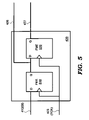
- FIG. 5 is a block diagram of a de-multiplexer block in an embodiment of the present invention.
- FIG. 6 is an example timing diagram illustrating the de-multiplexing of a test vector into sub-chains in an embodiment of the present invention.
- FIG. 7 is a block diagram of a multiplexer block in an embodiment of the present invention.
- FIG. 8 is an example timing diagram illustrating the multiplexing of response vectors from sub-chains to form a single serial output stream in an embodiment of the present invention.
- test vector is scanned serially into a functional memory element at a first frequency, which then de-multiplexes the bits in the test vector to multiple sub-chains at a lower frequency.
- FIG. 1 is a block diagram of an example integrated circuit (IC) in which several aspects of the present invention can be implemented.
- IC 100 is shown containing functional memory elements (FME) 110 A through FME 110 N, boundary scan registers BSR 120 , BSR 130 and BSR 140 , and IC pins 150 , 160 and 170 .
- FME functional memory elements
- BSR 120 boundary scan registers
- BSR 130 boundary scan registers
- BSR 140 IC pins
- IC pins 150 , 160 and 170 IC pins
- Components that implement the desired operational features of IC 100 are indicated in the Figure as being contained in functional portion 180 .
- Operational features refer to the features provided during normal operation of the integrated circuit and the components operative when providing the operational features (even though used for testing also according to scan techniques, as described below) of the IC are deemed to be contained in the functional portion.
- components such as boundary scan registers are not used to provide operational features (and used exclusively for testing), and are therefore deemed not to be functional components.
- BSRs 120 , 130 and 140 represent boundary scan cells used to implement boundary scan testing, for example, according to IEEE 1149.1 standard.
- Each of BSR 120 , 130 and 140 maybe a flip flop (memory element) and is associated with a corresponding IC pin used for input/output.
- BSR 120 is associated with pin 150
- BSR 130 is associated with pin 160
- BSR 140 is associated with pin 170 , and the bit value in each BSR may be provided to the corresponding pin. It may be appreciated that each BSR is associated with a single corresponding I/O pin and thus the number of BSRs is generally limited.
- Boundary scan cells such as BSR 120 , BSR 130 and BSR 140 are configured to form a boundary scan register during a boundary scan test mode.
- the boundary scan register is controlled by a state machine (not shown) that can be accessed through a four or five pin Test Access Port (TAP, not shown) at the chip's boundary.
- TAP Test Access Port
- the state machine loads various instructions that enable the generation of desired signals on the IC pins via the boundary scan cells.
- IC 100 is a processor chip (with portion 180 being the central processing unit—CPU), and is connected to an external memory (not shown)
- memory read/memory write cycles may be generated by loading the corresponding signal (bit) values in the boundary scan cells, and providing the values on the pins that connect to the memory.
- Boundary scan cells are operational only during such testing operations, and are in a power-down mode during normal operation of IC 100 . For example, when CPU 180 is operational (to perform corresponding CPU related operations), boundary scan cells are disabled.
- Functional memory elements (FME) 110 A- 110 N represent memory storage elements (e.g, flip-flops) used in implementing operational features of IC 100 , in addition to facilitating the testing of the IC. Due to such use, the FMEs are powered-on (contrary to the operation of the boundary scan cells) during normal operation. With respect to the example noted above, assuming that portion 180 is a central processing unit (CPU), FMEs 110 A- 110 N maybe used as part of corresponding circuitry that implements the CPU.
- CPU central processing unit
- FME 110 A through 110 N are configured as a scan chain (scan chain 1 , in FIG. 1 ), with the output of one memory element being connected to the input of a next memory element.
- scan chain 1 scan chain 1 , in FIG. 1
- output 162 of FME 110 A is connected to the input of FME 110 B
- output 163 of FME 110 B is connected to the input of FME 110 C (not shown), and so forth.
- Each of FME 110 A through 110 N may be clocked by a clock signal 170 (provided externally on pin/path 170 ). Test vectors are shifted in to scan chain 1 from an external test equipment (not shown) via pin/path 160 . The output of scan chain 1 is provided from the last flip flop 110 N in the scan chain to the external test equipment via pin/path 150 .
- IC 100 may contain several such scan chains. Details of the operation of a portion of scan chain 1 during a scan test are described next.
- FIG. 2 is a block diagram illustrating the operation of a portion of a scan chain during a scan test.
- FIG. 2 is shown containing FME 110 A, FME 110 B (of FIG. 1 ), and combinational logic 230 . Though not shown in FIG. 1 , combinational logic 230 is also part of CPU 180 of FIG. 1 .
- FME 110 A is shown containing multiplexer (MUX) 210 and flip-flop (FF) 220 .
- MUX 210 receives the corresponding bits of a test vector (in serial form) on path 160 , and a functional input on path 201 .
- the functional input on path 201 may be received from another flip flop (not shown) in circuit portion 180 .
- MUX 210 provides one of inputs 160 and 201 on path 212 to FF 220 depending on the value of a select bit on path 202 .
- the select bit on path 202 may be controlled from an external test equipment such that the bit is set to one value during testing and another value during normal operation.
- FF 220 transfers the bit received on path 212 as an output bit on path 162 in response to clock signal 170 .
- Combinational logic 230 receives an input on path 162 , and provides an output on path 234 .
- Output 234 contains the result of the combinational logic operation performed on input 162 by combination logic 230 .
- Paths such as path 162 -combinational logic 230 -path 234 are often termed functional paths.
- a single combinational logic 230 being tested based on inputs from a single memory cell.
- an integrated circuit typically contains many such logics, which are tested based on multiple inputs received from respective FMEs.
- FME 110 B is shown containing multiplexer (MUX) 240 and flip-flop (FF) 250 .
- MUX 240 provides one of inputs 162 and 234 on path 245 to FF 250 depending on the value of the select bit on path 202 .
- FF 250 provides an output bit on path 163 , which may be connected to a next (FME 110 C, not shown) memory element in the scan chain.
- FF 220 and 250 receive a clock signal on path 170 .
- select bit 202 (scan enable) is activated to cause MUX 210 to provide input 160 on path 162 , and MUX 240 to provide input 162 on path 245 .
- a test vector is then shifted into scan chain 1 by clock 170 . Consequently, corresponding test bits are stored in FF 220 and FF 250 .
- scan enable 202 is deactivated.
- MUX 240 provides output 234 of combinational logic 230 on path 245 to FF 250 .
- a capture pulse is applied on clock 170 .
- the output of combinational logic 230 is captured by FF 250 . It may be appreciated that scan enable 202 is deactivated even during the normal operation of the integrated circuit.
- flip flops similarly capture the response of corresponding combinational logic blocks.
- the operation of providing test bits of the test vector to the combination logic blocks, and capturing the corresponding outputs of the combinational logic blocks is generally termed as performing a functional test.
- Scan enable 202 is then activated again, and the response (outputs) of the combinational logic blocks to the test vector is shifted out via path 150 ( FIG. 1 ).
- test time may consume a large amount of time.
- Test time may be reduced by increasing the frequency of clock 170 used for shifting in and shifting out.
- such an approach may cause proportionately more power to be dissipated in the memory elements (in a given time duration), and potentially violate the maximum power rating of the integrated circuit.
- Various aspects of the present invention provide a scalable scan-based architecture that enables minimizing both test time as well as power consumption during a scan test, as described next with respect to a flowchart.
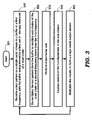
- FIG. 3 is a flowchart illustrating the manner in which a scan-based test can be performed in an embodiment of the present invention.
- the flowchart is described with respect to FIG. 1 , and in relation to IC 100 , merely for illustration. However, various features can be implemented in other environments and with other components. Furthermore, the steps are described in a specific sequence merely for illustration.
- step 301 control passes immediately to step 310 .
- step 310 IC 100 receives a test pattern in a single serial stream in a buffer at a first frequency, with the buffer being formed by a first set of functional memory elements of a scan chain.
- the first frequency may be selected to be sufficiently high such that test time is minimized. Control then passes to step 320 .
- step 320 the test pattern received in the buffer is de-multiplexed to multiple sub-chains of the scan chain at a second frequency lower than the first frequency.
- the sub-chains contain other functional memory elements (not included in the first set) of the scan chain.
- the second frequency is generally chosen such that power consumption in the components of the scan chain is below a desired level. Control then passes to step 330 .
- step 330 a functional test is performed. As noted above, during a functional test, the respective test bits in the test pattern are provided to corresponding combinational logic blocks. Control then passes to step 340 .
- step 340 results of the functional test are captured back in the sub-chains. Control then passes to step 350 .
- step 350 the result bits are multiplexed to form a single serial output stream. Control then passes to step 310 , and steps 310 through 350 may be repeated to perform another functional test.
- FIG. 4 is a block diagram of an IC implementing a scan-based test architecture in an embodiment of the present invention.
- IC 400 is shown containing scan splitter block 410 , functional memory elements 460 A- 460 N, and functional memory elements 470 A- 470 N. Each block is described in detail below.
- Functional memory elements 460 A- 460 N and 470 A- 47 ON are shown connected to from two sub-chains 460 and 470 respectively. Within each sub-chain, the corresponding functional memory elements are connected serially, with the output of functional memory element being provided as input to a next functional memory element.
- output of FME 460 A is provided as input to FME 460 B (in sub-chain 460 )
- output of FME 470 A is provided as input to FME 470 B (in sub-chain 470 ), etc, in a manner similar to that described above with respect to FIG. 1 .
- the outputs of each FME 460 A- 460 N and 470 A- 470 N is also connected to a corresponding combinational logic block to be tested (similar to combination logic 230 shown in FIG. 2 ).
- Scan splitter block 410 receives a test vector on path 412 and de-multiplexes the test vector into sub-vectors provided on paths 426 and 427 respectively. Each of the vectors contains a corresponding sequence of bits. In the described embodiments, alternative bits are provided on the paths 426 and 427 , however, other approaches can be chosen as suited in the specific environments. According to an aspect of the present invention, scan splitter block 410 is implemented using one or more functional memory elements, which are also used during normal operation of the IC 400 .
- scan splitter block 410 is shown containing de-multiplexer (DEMUX) block 420 , clock divider block 430 and multiplexer (MUX) block 440 .
- DEMUX block 420 receives a test vector (SI) in serial form on path 412 , stores (buffers) the serial test vector, and demultiplexes the test vector on path 426 to sub-chain 460 , and path 427 to sub-chain 470 .
- DEMUX block 420 also receives test clock (TCK).
- Scan splitter block 410 receives the bits on path 412 at twice the speed compared to the bits transmitted in each of paths 426 and 427 in the present example.
- Clock divider block 430 receives a test clock (TCK) on path 423 , and provides on path 436 a lower speed clock (for example, obtained by dividing TCK 423 ) to the functional memory elements in sub-chains 460 and 470 .
- Clock divider block 430 also generates a ‘select’ clock 434 provided to MUX block 440 .
- An external test equipment may provide SI and TCK.
- Clock divider block 430 may be implemented in a known way.
- MUX block 440 receives serial streams containing the response (result) of a functional test from sub-chains 460 and 470 on paths 446 and 447 respectively, multiplexes the multiple streams to form a single output stream (SO) provided on path 443 .
- An external test equipment may receive the output stream.
- MUX block 440 also receives test clock (TCK) and provides each of the bits according to TCK.
- Paths 412 , 423 and 443 may be connected to pins of IC 400 .
- scan splitter block 410 may demultiplex a received test vector across all of such sub-chains, and multiplex result streams from all such sub-chains to form a single output stream.
- scan splitter block 410 in an embodiment of the present invention is described below.
- FIG. 5 is a block diagram of a de-multiplexer block in an embodiment of the present invention.
- DEMUX block 420 is shown containing FME 510 and FME 520 . Both FME 510 and 520 receive a test clock on path 423 .
- FME 510 receives on path 412 (SI) bits of a test vector in serial form, and stores each bit at a time instance specified by an edge of clock 423 .
- FME 510 provides the stored bit as input to FME 520 , as well as on path 426 to sub-chain 460 ( FIG. 4 ).
- FME 520 stores the input on received from FME 510 at an edge of clock 423 , and provides the stored bit on path 427 to sub-chain 470 ( FIG. 4 ).
- DEMUX block 420 operates as a buffer, receiving (storing) bits of a test vector at a higher frequency (frequency of clock 423 ), and de-multiplexing the received bits on paths 426 and 427 in the form of corresponding sub-vectors.
- the bits multiplexed by DEMUX block 420 are shifted through sub-chains 460 and 470 at a lower frequency by divided clock 436 ( FIG. 4 ).
- the clock signal on path 436 has a frequency half that of the clock signal on path 423 .
- FIG. 6 is an example timing diagram illustrating the relative time instances (with respect to clocks 423 and 436 ) at which bits received on path 412 are stored (in the process of shifting-in) in FMEs 510 , 520 , and FMEs 460 A and 470 A ( FIG. 4 ). For simplicity only a few illustrative cycles (corresponding to storage of four bits of the test vector) are illustrated in the Figure.
- the bit stored in FME 510 at clock edge 610 of clock 423 is stored in FME 460 A at the clock edge 650 of clock 436 .
- the bit stored in FME 520 at clock edge 620 of clock 423 is stored in FME 470 A also at the clock edge 650 of clock 436 .
- the bits stored in FME 510 at clock edge 630 of clock 423 and FME 520 at clock edge 640 of clock 423 are respectively stored in FME 460 A and FME 470 A at clock edge 660 of clock 436 . It may be noted that clock edges 630 and 650 occur substantially simultaneously.
- bit sequence 0110 (being a portion of the test vector received on path 412 ) is assumed to be shifted in via path 412 , with the bits 0 , 1 , 1 and 0 corresponding to clock edges 610 , 620 , 630 and 640 respectively, at edge clock edge 650 FME 510 and 520 respectively store a 0 and 1 , while at edge clock edge 660 FME 510 and 520 respectively store a 1 and 0 .
- bits of the test vector are shifted through sub-chains 460 and 470 at half the rate at which the bits are received in DEMUX block 420 . Since there are two sub-chains as many bits are shifted in through the sub-chains as are received on pin 412 . However, each functional memory element in a sub-chain is toggled only at half the frequency.
- test time is decreased while reducing test power.
- the scan frequency is to be increased further to 32 MHz (to further reduce test time)
- internal shift frequency being maintained at 8 MHz
- four sub-chains may be used, with one test bit being provided to each of the four sub-chains in one clock cycle duration of the internal 8 Mhz clock, i.e., in 125 nano seconds.
- the reduction in test time is approximately 37%.
- dynamic test power will reduce by approximately 20% since the dynamic test power is directly proportional to frequency.
- test pin count number of test pins (test pin count) to be reduced.
- test pin count number of test pins (test pin count) to be reduced.
- scan chain 1 and scan chain 2 the test bits corresponding to both the scan chains
- Scan splitter block 410 may be implemented to split the single serial stream into two sub-chains, with each sub-chain now corresponding to scan chain 1 and scan chain 2 respectively.
- the response of the sub-chains may be multiplexed onto a single pin. Thus, only 2 pins (a relative reduction of 50%) are required for supporting both the scan chains.
- each of the scan chains 1 and 2 may be further split into two sub-chains each, with a total of four sub-chains.
- DEMUX block 420 may be implemented as 1:4 de-multiplexer
- MUX block 440 may be implemented as a 4:1 multiplexer
- clock divider block 430 generating a divide-by-4 clock to drive the corresponding sub-chains.
- the techniques of the present invention enable reducing test time, test power as well as test pin-count simultaneously.
- the technique can be customized to reduce one or more of the three factors (test time, test power, test pin count) in scan based testing.
- the reduction in test time is approximately 1/N of the “original” test time (i.e., test time required when test vector is not demultiplexed to multiple sub-chains).
- the approximate reduction in test power is 1/N of the “original” test power
- the reduction in test pin-count is 1/N of the “original” test pin-count required to test the IC.
- the scan-based test architecture described above is scalable to support potentially any number of scan chains simultaneously.
- the technique described above requires fewer number of pins to be connected from an external tester. Assuming that the technique of multiplexing and de-multiplexing of the present invention were not used, the number of scan chains would generally depend on (and limited by) the number of pins available for scan-ins and scan-outs (similar to pins 412 and 443 respectively).
- a multiplexer block used in an embodiment of the present invention is described next.
- FIG. 7 is a block diagram of a multiplexer block in an embodiment of the present invention.
- MUX block 440 is shown containing FME 710 and multiplexer 730 .
- FME 710 receives test clock (TCK) 423 .
- TCK test clock
- Multiplexer 730 receives response bits (results of a functional test on corresponding combinational logic blocks) from sub-chain 460 on path 446 , as well as response bits from sub-chain 470 on path 447 . Multiplexer 730 provides on path 731 either of the bits on path 446 or the bits on path 447 based on the value of the select signal on path 434 .
- FME 710 receives bits forwarded by multiplexer 730 on path 731 , and provides (at time instances specified by an edge of clock 423 ) the bits as a single serial output stream on path 443 (SO) as the response to a functional test.
- FIG. 8 is an example timing diagram illustrating the relative time instances (with respect to clocks 423 , 436 and 434 ) at which response bits in the output stream are provided on path 443 . For simplicity only a few illustrative cycles (corresponding to four bits of the output stream) are illustrated in the Figure. In the Figure it is assumed that multiplexer 730 forwards input 446 on path 731 when select signal 434 is at logic high, and forwards input 447 on path 731 when select signal 434 is at logic low
- each of FME 460 N and FME 470 N ( FIG. 4 ) provide an output bit (respectively on paths 446 and 447 ) at clock edge 810 of clock 423 .
- select signal 434 is at logic high, and multiplexer 730 forwards the bit on path 446 on path 731 . Therefore, FME 710 provides the bit on path 446 on output 443 .
- select signal 434 is at logic low, and multiplexer 730 forwards the bit on path 447 on path 731 . Therefore, FME 710 provides the bit on path 447 on output 443 . Similarly, the respective bits provided by FME 460 N and FME 470 N at clock edge 820 are shifted out on output 443 at clock edges 850 and 860 respectively. It may be noted that clock edges 820 and 840 may occur substantially simultaneously.
- DEMUX block 420 is described as containing two functional memory elements, alternative embodiments of DEMUX block 420 may be implemented using more or fewer than two functional memory elements, and/or different combination of components and interconnections.
- DEMUX block 420 may be implemented to contain only one functional memory element (for example only FME 510 ) to perform a multiplexing operation.
- FME 510 receives test vectors at the frequency of clock 423 , and elements of sub-chains 460 and 470 may be clocked by anti-phase clocks (phase difference of 180 degrees) at half (or some divided) frequency of clock 423 .
- FME 460 A and FME 470 A store every alternate output of FME 510 .
- MUX block 440 may be similarly modified to contain only one functional memory element.
- the functional memory elements of FIGS. 5 and 7 would each provide an input to combinational logic at least in some scenarios of normal operation of IC 400 .
- the functional memory elements can also provide inputs to respective combinational logics in the functional test mode as well, depending on the specific portions of the integrated circuit being tested. Further, assuming that several scan splitter blocks (similar to scan splitter block 410 ) are present, the functional memory elements in such scan splitter blocks may be connected as a separate (single) scan chain, and scan test may be performed to test the corresponding combinational logic blocks.
Landscapes
- Engineering & Computer Science (AREA)
- General Engineering & Computer Science (AREA)
- Physics & Mathematics (AREA)
- General Physics & Mathematics (AREA)
- Power Engineering (AREA)
- Tests Of Electronic Circuits (AREA)
Abstract
A scalable scan-based architecture with reduced test time, test power and test pin-count in scan based testing of ICs. In an embodiment, a test vector is scanned serially into a functional memory element at a first frequency, which then de-multiplexes the bits in the test vector to multiple sub-chains at a lower frequency. Due to the use of lower frequency to scan-in, the power dissipation is reduced. Due to the use of the higher frequency to scan-in the test vector as well as multiple sub-chains, the test time is reduced. Due to the use of the functional memory elements for scanning in the test vector at higher frequency, any number of chains can potentially be supported.
Description
- 1. Field of Disclosure
- The present disclosure relates generally to Integrated Circuit testing, and more specifically to a scalable scan-based architecture with reduced test time and power consumed during testing.
- 2. Related Art
- Integrated circuits (IC) generally need to be tested after fabrication. One technique for testing ICs is scan-based testing. Scan-based testing generally refers to a technique in which registers (or more generally storage elements) in the IC are connected serially to form a shift register, often termed a scan chain. A test pattern (test vector) from an external test equipment is then shifted serially into the scan chain.
- Once the test vector is loaded in the scan chain, a functional test is performed, with each bit in the test vector being provided as in input to a corresponding combinational logic. The output bit of each combinational logic is captured back in a scan chain, and the captured data is then shifted out to the test equipment. The test equipment then compares the captured data with a desired response.
- It is generally desirable to reduce test time, and power consumed. Test time during a scan-based test generally refers to the total length of time needed to load (serially shift in) a test vector into a scan chain, perform a functional test and provide (serially shift out) the results of the test. Test time is inversely proportional to the speed (frequency) at which the test vector and response are shifted through the scan chain.
- On the other hand, power consumed in the IC during testing is generally directly proportional to frequency at which the test vector and response are shifted through the scan chain. In general, it is desirable that a scan-based test architecture reduce both the test time as well as the power consumed in an IC during a scan-based test.
- It may be desirable that the approach also be scalable. Scalability of a scan-based test architecture generally refers to the ability of the architecture/approach to accommodate a larger number of flip-flops. The approach often needs to be designed while keeping the test time and power consumption within acceptable levels.
- Several aspects of the present invention provide a scalable scan-based test architecture with at least one of reduced test time and power.
- Example embodiments will be described with reference to the following accompanying drawings, which are described briefly below.
-
FIG. 1 is a block diagram of an example integrated circuit (IC) in which several aspects of the present invention can be implemented. -
FIG. 2 is a block diagram illustrating the operation of a portion of a scan chain during scan test. -
FIG. 3 is a flowchart illustrating the manner in which a scan-based test can be performed in an embodiment of the present invention. -
FIG. 4 is a block diagram of an IC implementing a scan-based test architecture in an embodiment of the present invention. -
FIG. 5 is a block diagram of a de-multiplexer block in an embodiment of the present invention. -
FIG. 6 is an example timing diagram illustrating the de-multiplexing of a test vector into sub-chains in an embodiment of the present invention. -
FIG. 7 is a block diagram of a multiplexer block in an embodiment of the present invention. -
FIG. 8 is an example timing diagram illustrating the multiplexing of response vectors from sub-chains to form a single serial output stream in an embodiment of the present invention. - In the drawings, like reference numbers generally indicate identical, functionally similar, and/or structurally similar elements. The drawing in which an element first appears is indicated by the leftmost digit(s) in the corresponding reference number.
- 1. Overview
- An aspect of the present invention provides a scalable scan-based architecture with reduced test time, and power consumed during testing. In an embodiment, the test vector is scanned serially into a functional memory element at a first frequency, which then de-multiplexes the bits in the test vector to multiple sub-chains at a lower frequency.
- Due to the use of lower frequency in load and unload of test vector into the scan chains, the power dissipation is reduced. Due to the use of the higher frequency to shift-in and shift-out the test vector into the IC the test time is reduced. Due to the use of the functional memory elements for scanning in the test vector at higher frequency, any number of chains can potentially be supported.
- Several aspects of the invention are described below with reference to examples for illustration. It should be understood that numerous specific details, relationships, and methods are set forth to provide a full understanding of the invention. One skilled in the relevant arts, however, will readily recognize that the invention can be practiced without one or more of the specific details, or with other methods, etc. In other instances, well-known structures or operations are not shown in detail to avoid obscuring the features of the invention.
- 2. Integrated Circuit
-
FIG. 1 is a block diagram of an example integrated circuit (IC) in which several aspects of the present invention can be implemented. IC 100 is shown containing functional memory elements (FME) 110A through FME 110N, boundaryscan registers BSR 120, BSR 130 and BSR 140, andIC pins FIG. 1 are merely for illustrative purposes, and a typical IC contains many more components, both in number and types. Each block is described below in further detail. - Components (including FME 110A through 110N) that implement the desired operational features of
IC 100 are indicated in the Figure as being contained infunctional portion 180. Operational features refer to the features provided during normal operation of the integrated circuit and the components operative when providing the operational features (even though used for testing also according to scan techniques, as described below) of the IC are deemed to be contained in the functional portion. In contrast, as described below, components such as boundary scan registers are not used to provide operational features (and used exclusively for testing), and are therefore deemed not to be functional components. -
BSRs BSR pin 150, BSR 130 is associated withpin 160, and BSR 140 is associated withpin 170, and the bit value in each BSR may be provided to the corresponding pin. It may be appreciated that each BSR is associated with a single corresponding I/O pin and thus the number of BSRs is generally limited. - As is well known in the relevant arts, the IEEE 1149.1 standard is used to test circuit components on a printed circuit board (PCB). Boundary scan cells such as
BSR 120, BSR 130 and BSR 140 are configured to form a boundary scan register during a boundary scan test mode. The boundary scan register is controlled by a state machine (not shown) that can be accessed through a four or five pin Test Access Port (TAP, not shown) at the chip's boundary. - The state machine loads various instructions that enable the generation of desired signals on the IC pins via the boundary scan cells. As an example, assuming
IC 100 is a processor chip (withportion 180 being the central processing unit—CPU), and is connected to an external memory (not shown), memory read/memory write cycles may be generated by loading the corresponding signal (bit) values in the boundary scan cells, and providing the values on the pins that connect to the memory. - Boundary scan cells (as well as the TAP) are operational only during such testing operations, and are in a power-down mode during normal operation of
IC 100. For example, whenCPU 180 is operational (to perform corresponding CPU related operations), boundary scan cells are disabled. - Functional memory elements (FME) 110A-110N represent memory storage elements (e.g, flip-flops) used in implementing operational features of
IC 100, in addition to facilitating the testing of the IC. Due to such use, the FMEs are powered-on (contrary to the operation of the boundary scan cells) during normal operation. With respect to the example noted above, assuming thatportion 180 is a central processing unit (CPU),FMEs 110A-110N maybe used as part of corresponding circuitry that implements the CPU. - As is well known in the relevant arts, components of CPU 180 (typically combinational logic) may be tested after fabrication using scan-based test approaches. As noted above, in such scan-based
test FME 110A through 110N are configured as a scan chain (scanchain 1, inFIG. 1 ), with the output of one memory element being connected to the input of a next memory element. Thus, as shown inFIG. 1 , during a scan test,output 162 ofFME 110A is connected to the input ofFME 110B,output 163 ofFME 110B is connected to the input of FME 110C (not shown), and so forth. - Each of
FME 110A through 110N may be clocked by a clock signal 170 (provided externally on pin/path 170). Test vectors are shifted in to scanchain 1 from an external test equipment (not shown) via pin/path 160. The output ofscan chain 1 is provided from thelast flip flop 110N in the scan chain to the external test equipment via pin/path 150. - Although not shown in
FIG. 1 ,IC 100 may contain several such scan chains. Details of the operation of a portion ofscan chain 1 during a scan test are described next. - 3. Scan Test
-
FIG. 2 is a block diagram illustrating the operation of a portion of a scan chain during a scan test.FIG. 2 is shown containingFME 110A,FME 110B (ofFIG. 1 ), andcombinational logic 230. Though not shown inFIG. 1 ,combinational logic 230 is also part ofCPU 180 ofFIG. 1 . -
FME 110A is shown containing multiplexer (MUX) 210 and flip-flop (FF) 220.MUX 210 receives the corresponding bits of a test vector (in serial form) onpath 160, and a functional input onpath 201. The functional input onpath 201 may be received from another flip flop (not shown) incircuit portion 180.MUX 210 provides one ofinputs path 212 toFF 220 depending on the value of a select bit onpath 202. The select bit onpath 202 may be controlled from an external test equipment such that the bit is set to one value during testing and another value during normal operation.FF 220 transfers the bit received onpath 212 as an output bit onpath 162 in response toclock signal 170. -
Combinational logic 230 receives an input onpath 162, and provides an output onpath 234.Output 234 contains the result of the combinational logic operation performed oninput 162 bycombination logic 230. Paths such as path 162-combinational logic 230-path 234 are often termed functional paths. Merely for conciseness, only asingle combinational logic 230 being tested based on inputs from a single memory cell. However, in real-world implementations, an integrated circuit typically contains many such logics, which are tested based on multiple inputs received from respective FMEs. -
FME 110B is shown containing multiplexer (MUX) 240 and flip-flop (FF) 250.MUX 240 provides one ofinputs path 245 to FF 250 depending on the value of the select bit onpath 202. FF 250 provides an output bit onpath 163, which may be connected to a next (FME 110C, not shown) memory element in the scan chain.FF 220 and 250 receive a clock signal onpath 170. - During a scan test, select bit 202 (scan enable) is activated to cause
MUX 210 to provideinput 160 onpath 162, andMUX 240 to provideinput 162 onpath 245. A test vector is then shifted intoscan chain 1 byclock 170. Consequently, corresponding test bits are stored inFF 220 and FF 250. - Once the test vector is shifted into
scan chain 1, scan enable 202 is deactivated. As a result, each memory element (and corresponding flip flop) receives the output of the corresponding combination logic. For example,MUX 240 providesoutput 234 ofcombinational logic 230 onpath 245 to FF 250. A capture pulse is applied onclock 170. As a result, the output ofcombinational logic 230 is captured by FF 250. It may be appreciated that scan enable 202 is deactivated even during the normal operation of the integrated circuit. - Other flip flops (not shown) similarly capture the response of corresponding combinational logic blocks. The operation of providing test bits of the test vector to the combination logic blocks, and capturing the corresponding outputs of the combinational logic blocks is generally termed as performing a functional test.
- Scan enable 202 is then activated again, and the response (outputs) of the combinational logic blocks to the test vector is shifted out via path 150 (
FIG. 1 ). - Since the number of memory elements in a scan chain (e.g., scan chain 1) is typically large, shifting in the test vector and shifting out the response (test time) may consume a large amount of time. Test time may be reduced by increasing the frequency of
clock 170 used for shifting in and shifting out. However, such an approach may cause proportionately more power to be dissipated in the memory elements (in a given time duration), and potentially violate the maximum power rating of the integrated circuit. - Various aspects of the present invention provide a scalable scan-based architecture that enables minimizing both test time as well as power consumption during a scan test, as described next with respect to a flowchart.
- 4. Approach
-
FIG. 3 is a flowchart illustrating the manner in which a scan-based test can be performed in an embodiment of the present invention. The flowchart is described with respect toFIG. 1 , and in relation toIC 100, merely for illustration. However, various features can be implemented in other environments and with other components. Furthermore, the steps are described in a specific sequence merely for illustration. - Alternative embodiments in other environments, using other components and different sequence of steps can also be implemented without departing from the scope and spirit of several aspects of the present invention, as will be apparent to one skilled in the relevant arts by reading the disclosure provided herein. The flowchart starts in
step 301, in which control passes immediately to step 310. - In
step 310,IC 100 receives a test pattern in a single serial stream in a buffer at a first frequency, with the buffer being formed by a first set of functional memory elements of a scan chain. The first frequency may be selected to be sufficiently high such that test time is minimized. Control then passes to step 320. - In
step 320, the test pattern received in the buffer is de-multiplexed to multiple sub-chains of the scan chain at a second frequency lower than the first frequency. The sub-chains contain other functional memory elements (not included in the first set) of the scan chain. The second frequency is generally chosen such that power consumption in the components of the scan chain is below a desired level. Control then passes to step 330. - In
step 330, a functional test is performed. As noted above, during a functional test, the respective test bits in the test pattern are provided to corresponding combinational logic blocks. Control then passes to step 340. - In
step 340, results of the functional test are captured back in the sub-chains. Control then passes to step 350. - In
step 350, the result bits are multiplexed to form a single serial output stream. Control then passes to step 310, and steps 310 through 350 may be repeated to perform another functional test. - The features described above can be implemented using various approaches. The manner in which the approach described above may be implemented is described next with examples.
- 5. Architecture
-
FIG. 4 is a block diagram of an IC implementing a scan-based test architecture in an embodiment of the present invention.IC 400 is shown containingscan splitter block 410,functional memory elements 460A-460N, andfunctional memory elements 470A-470N. Each block is described in detail below. -
Functional memory elements 460A-460N and 470A-47ON are shown connected to from twosub-chains - Thus, output of
FME 460A is provided as input toFME 460B (in sub-chain 460), output ofFME 470A is provided as input toFME 470B (in sub-chain 470), etc, in a manner similar to that described above with respect toFIG. 1 . Although not shown, the outputs of eachFME 460A-460N and 470A-470N is also connected to a corresponding combinational logic block to be tested (similar tocombination logic 230 shown inFIG. 2 ). -
Scan splitter block 410 receives a test vector onpath 412 and de-multiplexes the test vector into sub-vectors provided onpaths paths splitter block 410 is implemented using one or more functional memory elements, which are also used during normal operation of theIC 400. - In the example of
FIG. 4 , scansplitter block 410 is shown containing de-multiplexer (DEMUX) block 420,clock divider block 430 and multiplexer (MUX)block 440.DEMUX block 420 receives a test vector (SI) in serial form onpath 412, stores (buffers) the serial test vector, and demultiplexes the test vector onpath 426 to sub-chain 460, andpath 427 to sub-chain 470. DEMUX block 420 also receives test clock (TCK).Scan splitter block 410 receives the bits onpath 412 at twice the speed compared to the bits transmitted in each ofpaths -
Clock divider block 430 receives a test clock (TCK) onpath 423, and provides on path 436 a lower speed clock (for example, obtained by dividing TCK 423) to the functional memory elements insub-chains Clock divider block 430 also generates a ‘select’clock 434 provided toMUX block 440. An external test equipment may provide SI and TCK.Clock divider block 430 may be implemented in a known way. -
MUX block 440 receives serial streams containing the response (result) of a functional test fromsub-chains paths path 443. An external test equipment may receive the output stream.MUX block 440 also receives test clock (TCK) and provides each of the bits according to TCK.Paths IC 400. - Although only two sub-chains are shown in
FIG. 4 , it must be understood that any number of sub-chains similar to 460 and 470 may be created, and scansplitter block 410 may demultiplex a received test vector across all of such sub-chains, and multiplex result streams from all such sub-chains to form a single output stream. - The internal details of
scan splitter block 410 in an embodiment of the present invention are described below. - 6. De-Multiplexer Block
-
FIG. 5 is a block diagram of a de-multiplexer block in an embodiment of the present invention.DEMUX block 420 is shown containingFME 510 andFME 520. BothFME path 423. -
FME 510 receives on path 412 (SI) bits of a test vector in serial form, and stores each bit at a time instance specified by an edge ofclock 423.FME 510 provides the stored bit as input toFME 520, as well as onpath 426 to sub-chain 460 (FIG. 4 ).FME 520 stores the input on received fromFME 510 at an edge ofclock 423, and provides the stored bit onpath 427 to sub-chain 470 (FIG. 4 ). - It may be appreciated that
DEMUX block 420 operates as a buffer, receiving (storing) bits of a test vector at a higher frequency (frequency of clock 423), and de-multiplexing the received bits onpaths - As noted above, the bits multiplexed by
DEMUX block 420 are shifted throughsub-chains FIG. 4 ). In an embodiment the clock signal onpath 436 has a frequency half that of the clock signal onpath 423. -
FIG. 6 is an example timing diagram illustrating the relative time instances (with respect toclocks 423 and 436) at which bits received onpath 412 are stored (in the process of shifting-in) inFMEs FMEs FIG. 4 ). For simplicity only a few illustrative cycles (corresponding to storage of four bits of the test vector) are illustrated in the Figure. - With respect to
FIG. 6 , the bit stored inFME 510 at clock edge610 ofclock 423 is stored inFME 460A at the clock edge650 ofclock 436. The bit stored inFME 520 at clock edge620 ofclock 423 is stored inFME 470A also at the clock edge650 ofclock 436. Similarly, the bits stored inFME 510 at clock edge630 ofclock 423 andFME 520 at clock edge640 ofclock 423 are respectively stored inFME 460A andFME 470A at clock edge660 ofclock 436. It may be noted that clock edges 630 and 650 occur substantially simultaneously. - As an example, if the bit sequence 0110 (being a portion of the test vector received on path 412) is assumed to be shifted in via
path 412, with thebits edge clock edge 650FME edge clock edge 660FME - It may be appreciated that bits of the test vector are shifted through
sub-chains DEMUX block 420. Since there are two sub-chains as many bits are shifted in through the sub-chains as are received onpin 412. However, each functional memory element in a sub-chain is toggled only at half the frequency. - It may be appreciated that the technique described above enables test time to be decreased while reducing test power. As an example, assume that it is desired to increase the scan frequency (frequency of
clock 423 ofFIG. 4 ) from 10 MHz to 16 MHz to reduce test time. Since the shift frequency insub-chains sub-chains - Continuing with the example, assuming that the scan frequency is to be increased further to 32 MHz (to further reduce test time), with internal shift frequency being maintained at 8 MHz, four sub-chains may be used, with one test bit being provided to each of the four sub-chains in one clock cycle duration of the internal 8 Mhz clock, i.e., in 125 nano seconds. The reduction in test time is approximately 37%. At the same time, due to the reduction in internal shift frequency from 10 MHz to 8 MHz ( a reduction of 20%), dynamic test power will reduce by approximately 20% since the dynamic test power is directly proportional to frequency.
- Further, the features of the present invention may also enable the number of test pins (test pin count) to be reduced. To illustrate, assuming there are two (separate) scan chains to be tested, a prior approach may require four test pins (one scan-in pin and one scan-out pin for each of the scan chains). However, according to features of the present invention, the test bits corresponding to both the scan chains (referred to as
scan chain 1 and scan chain 2 below) may be provided from an external tester on a single pin. -
Scan splitter block 410 may be implemented to split the single serial stream into two sub-chains, with each sub-chain now corresponding to scanchain 1 and scan chain 2 respectively. The response of the sub-chains may be multiplexed onto a single pin. Thus, only 2 pins (a relative reduction of 50%) are required for supporting both the scan chains. - Alternatively, or in addition, each of the
scan chains 1 and 2, may be further split into two sub-chains each, with a total of four sub-chains.DEMUX block 420 may be implemented as 1:4 de-multiplexer, MUX block 440 may be implemented as a 4:1 multiplexer, withclock divider block 430 generating a divide-by-4 clock to drive the corresponding sub-chains. Again, only two pins to connect to an external tester would be required for the test, while reduction in test time and test power is also obtained at the same time. - Thus, it may be appreciated that the techniques of the present invention enable reducing test time, test power as well as test pin-count simultaneously. The technique can be customized to reduce one or more of the three factors (test time, test power, test pin count) in scan based testing.
- It is noted that even though the shift frequency within
DEMUX block 420 andMUX block 440 is at the same rate asclock 423, the number of FMEs in these blocks may be few, and thus do not appreciably cause an increase in power dissipation. - In general, when the number of sub-chains into which a scan vector (on path 412) is de-multiplexed equals “N” (with
scan splitter block 410 being termed an Nth order splitter), the reduction in test time is approximately 1/N of the “original” test time ( i.e., test time required when test vector is not demultiplexed to multiple sub-chains). Similarly, the approximate reduction in test power is 1/N of the “original” test power, and the reduction in test pin-count is 1/N of the “original” test pin-count required to test the IC. - Further, since a potentially large number of functional memory elements may be available in a functional portion of
IC 400, and since DEMUX and MUX blocks are implemented using functional memory elements, several blocks and corresponding sub-chains (similar to DEMUX block 420,MUX block 440 and sub-chains 460 and 470) may be operated simultaneously. Thus, the scan-based test architecture described above is scalable to support potentially any number of scan chains simultaneously. - It may also be appreciated that the technique described above requires fewer number of pins to be connected from an external tester. Assuming that the technique of multiplexing and de-multiplexing of the present invention were not used, the number of scan chains would generally depend on (and limited by) the number of pins available for scan-ins and scan-outs (similar to
pins - According to the approaches described above, since a single scan-in input (e.g., on pin 412) can be provided potentially to any number of parallel sub-chains, the total number of external pins for supporting multiple scan chains is reduced. Consequently, multiple scan chains (internal to an IC) can be tested using one pair of scan-in and scan-out pins (in general fewer scan-in and scan-out pins), with very little or no impact on test application time and/or test power consumption.
- A multiplexer block used in an embodiment of the present invention is described next.
- 7. Multiplexer Block
-
FIG. 7 is a block diagram of a multiplexer block in an embodiment of the present invention.MUX block 440 is shown containing FME 710 andmultiplexer 730. FME 710 receives test clock (TCK) 423. -
Multiplexer 730 receives response bits (results of a functional test on corresponding combinational logic blocks) fromsub-chain 460 onpath 446, as well as response bits from sub-chain 470 onpath 447.Multiplexer 730 provides onpath 731 either of the bits onpath 446 or the bits onpath 447 based on the value of the select signal onpath 434. - FME 710 receives bits forwarded by
multiplexer 730 onpath 731, and provides (at time instances specified by an edge of clock 423) the bits as a single serial output stream on path 443 (SO) as the response to a functional test. -
FIG. 8 is an example timing diagram illustrating the relative time instances (with respect toclocks path 443. For simplicity only a few illustrative cycles (corresponding to four bits of the output stream) are illustrated in the Figure. In the Figure it is assumed thatmultiplexer 730 forwards input 446 onpath 731 whenselect signal 434 is at logic high, and forwards input 447 onpath 731 whenselect signal 434 is at logic low - With respect to
FIG. 8 , it is assumed that each ofFME 460N andFME 470N (FIG. 4 ) provide an output bit (respectively onpaths 446 and 447) atclock edge 810 ofclock 423. Atclock edge 830 ofclock 423,select signal 434 is at logic high, andmultiplexer 730 forwards the bit onpath 446 onpath 731. Therefore, FME 710 provides the bit onpath 446 onoutput 443. - At
clock edge 840,select signal 434 is at logic low, andmultiplexer 730 forwards the bit onpath 447 onpath 731. Therefore, FME 710 provides the bit onpath 447 onoutput 443. Similarly, the respective bits provided byFME 460N andFME 470N atclock edge 820 are shifted out onoutput 443 at clock edges 850 and 860 respectively. It may be noted that clock edges 820 and 840 may occur substantially simultaneously. - It should be appreciated that several details described above are merely examples. Several alternative embodiments will be apparent to one skilled in the relevant arts by reading the disclosure provided herein. For example, though
DEMUX block 420 is described as containing two functional memory elements, alternative embodiments ofDEMUX block 420 may be implemented using more or fewer than two functional memory elements, and/or different combination of components and interconnections. - For example, DEMUX block 420 may be implemented to contain only one functional memory element (for example only FME 510) to perform a multiplexing operation. In such an example embodiment,
FME 510 receives test vectors at the frequency ofclock 423, and elements ofsub-chains clock 423. In such an embodiment,FME 460A andFME 470A store every alternate output ofFME 510.MUX block 440 may be similarly modified to contain only one functional memory element. - Though not expressly shown, the functional memory elements of
FIGS. 5 and 7 would each provide an input to combinational logic at least in some scenarios of normal operation ofIC 400. The functional memory elements can also provide inputs to respective combinational logics in the functional test mode as well, depending on the specific portions of the integrated circuit being tested. Further, assuming that several scan splitter blocks (similar to scan splitter block 410) are present, the functional memory elements in such scan splitter blocks may be connected as a separate (single) scan chain, and scan test may be performed to test the corresponding combinational logic blocks. - 8. Conclusion
- While various embodiments of the present invention have been described above, it should be understood that they have been presented by way of example only, and not limitation. Thus, the breadth and scope of the present invention should not be limited by any of the above described exemplary embodiments, but should be defined only in accordance with the following claims and their equivalents.
Claims (17)
1. A circuit comprising:
a first sub-chain containing a first sequence of functional memory elements;
a second sub-chain containing a second sequence of functional memory elements;
a scan splitter block formed from at least one functional memory element, said scan splitter block to receive a test vector containing a sequence of bits at a first frequency and to de-multiplex said sequence of bits such that a first subset of bits is sent to said first sub-chain and a second subset of bits is sent to said second sub-chain at a second frequency and a third frequency respectively in a scan mode, said first subset of bits and said second subset of bits being contained in said sequence of bits; and
a combinational logic to receive at least one input from said first sub-chain and said second sub-chain and to generate an output bit in a functional test mode,
wherein said first frequency is greater than each of said second frequency and said third frequency,
wherein said first sequence of functional memory elements, said second sequence of functional memory elements, and said at least one functional memory element are contained in a functional portion of said circuit.
2. The circuit of claim 1 , wherein said at least one functional memory element contains a same number of memory elements as a number of sub-chains including said first sub-chain and said second sub-chain.
3. The circuit of claim 2 , wherein said same number comprises two, wherein said second frequency is equal to said third frequency and also to half of said first frequency.
4. The circuit of claim 3 , wherein said scan splitter block comprises a clock divider which receives a clock signal with said first frequency and generates a divided clock signal at said second frequency, wherein said divided clock signal drives scanning into said first sub-chain and said second sub-chain and said clock signal is used to receive said sequence of bits.
5. The circuit of claim 4 , wherein said at least one functional memory element comprises:
a first functional memory element and a second functional memory element,
wherein an output of said first functional memory element is connected to an input of said second functional memory element and also as an input to said first sub-chain,
wherein an output of said second functional memory element is connected as an input to said second sub-chain,
both of said first functional memory element and said second functional memory element being clocked by said clock signal.
6. The circuit of claim 4 , wherein said scan splitter block further comprises at least one another functional memory element used to multiplex a first set of response bits from said first sub-chain and a second set of response bits from said second sub-chain to form a single serial output stream as a result of scan testing,
wherein said first set of response bits and said second set of response bits are generated by said combinational logic during said functional test mode.
7. The circuit of claim 6 , wherein said at least one another functional memory element comprises:
a multiplexer having a control input, a first input, a second input and an output, said multiplexer selecting a bit on either said first input or said second input based on said control input and providing the selected bit on said output, wherein said control input is designed to select respective bits from said first input and said second input in alternative clock cycles,
wherein said first input is coupled to receive said first set of response bits and said second input is coupled to receive said second set of response bits,
a third functional memory element receiving said output of said multiplexer,
wherein said third functional memory element is clocked by said clock signal such that said single serial output stream is provided as an output of said third functional memory element.
8. The circuit of claim 1 , wherein said at least one functional memory element contains a single functional memory element.
9. The circuit of claim 1 , further comprising a plurality of boundary scan registers.
10. An integrated circuit comprising:
means for receiving a test vector containing a sequence of bits at first frequency using at least one functional memory element;
means for de-multiplexing said test vector into a plurality of sub-chains in the form of a corresponding number of sub-vectors, each sub-chain containing a corresponding set of functional memory elements connected in series, wherein each sub-vector is scanned into the corresponding sub-chain at a frequency lower than said first frequency;
means for performing a functional test on a combinational logic contained in said integrated circuit after said de-multiplexing;
means for capturing in said plurality of sub-chains the results generated by said combinational logic in said functional test; and
means for examining said results to determine whether said integrated circuit operates according to a desired specification,
wherein the sets of functional memory elements and said at least one functional memory element together form a functional portion of said integrated circuit.
11. The integrated circuit of claim 10 , further comprising:
means for multiplexing the results captured by said plurality of sub-chains to form a single serial output stream,
wherein said examining examines said single serial output stream.
12. The integrated circuit of claim 11 , wherein said plurality of sub-chains comprises a first sub-chain and a second sub-chain, wherein each of a frequency at which a first sub-vector is scanned into said first sub-chain and a frequency at which a second sub-vector is scanned into said second sub-chain is equal to half of said first frequency, wherein said first sub-vector and said second sub-vector are contained in said sub-vectors.
13. A method of testing an integrated circuit, said method comprising:
receiving a test vector containing a sequence of bits at first frequency using at least one functional memory element;
de-multiplexing said test vector into a plurality of sub-chains in the form of a corresponding number of sub-vectors, each sub-chain containing a corresponding set of functional memory elements connected in series, wherein each sub-vector is scanned into the corresponding sub-chain at a frequency lower than said first frequency;
performing a functional test on a combinational logic contained in said integrated circuit after said de-multiplexing;
capturing in said plurality of sub-chains the results generated by said combinational logic in said functional test; and
examining said results to determine whether said integrated circuit operates according to a desired specification,
wherein the sets of functional memory elements and said at least one functional memory element together form a functional portion of said integrated circuit.
14. The method of claim 13 , further comprising:
multiplexing the results captured by said plurality of sub-chains to form a single serial output stream,
wherein said examining examines said single serial output stream.
15. The method of claim 14 , further comprising:
sending said single output stream at said first frequency to a test equipment, which performs said examining,
wherein the response bits in each of said plurality of sub-chains are received at said frequency lower than said first frequency.
16. The method of claim 14 , wherein said plurality of sub-chains comprises a first sub-chain and a second sub-chain, wherein each of a frequency at which a first sub-vector is scanned into said first sub-chain and a frequency at which a second sub-vector is scanned into said second sub-chain is equal to half of said first frequency, wherein said first sub-vector and said second sub-vector are contained in said sub-vectors.
17. The method of claim 13 , wherein said first frequency is an integral multiple of the frequency at which the sub-vectors are scanned into the corresponding sub-chains.
Priority Applications (1)
| Application Number | Priority Date | Filing Date | Title |
|---|---|---|---|
| US12/031,699 US8510616B2 (en) | 2008-02-14 | 2008-02-14 | Scalable scan-based test architecture with reduced test time and test power |
Applications Claiming Priority (1)
| Application Number | Priority Date | Filing Date | Title |
|---|---|---|---|
| US12/031,699 US8510616B2 (en) | 2008-02-14 | 2008-02-14 | Scalable scan-based test architecture with reduced test time and test power |
Publications (2)
| Publication Number | Publication Date |
|---|---|
| US20090210759A1 true US20090210759A1 (en) | 2009-08-20 |
| US8510616B2 US8510616B2 (en) | 2013-08-13 |
Family
ID=40956275
Family Applications (1)
| Application Number | Title | Priority Date | Filing Date |
|---|---|---|---|
| US12/031,699 Active 2028-05-03 US8510616B2 (en) | 2008-02-14 | 2008-02-14 | Scalable scan-based test architecture with reduced test time and test power |
Country Status (1)
| Country | Link |
|---|---|
| US (1) | US8510616B2 (en) |
Cited By (2)
| Publication number | Priority date | Publication date | Assignee | Title |
|---|---|---|---|---|
| CN103116069A (en) * | 2013-01-18 | 2013-05-22 | 深圳市海思半导体有限公司 | Method, device and system of testing of chip frequency |
| US9651623B2 (en) * | 2015-09-11 | 2017-05-16 | International Business Machines Corporation | Reducing power requirements and switching during logic built-in-self-test and scan test |
Families Citing this family (4)
| Publication number | Priority date | Publication date | Assignee | Title |
|---|---|---|---|---|
| US8745200B2 (en) * | 2008-05-06 | 2014-06-03 | Nvidia Corporation | Testing operation of processors setup to operate in different modes |
| US8943457B2 (en) * | 2008-11-24 | 2015-01-27 | Nvidia Corporation | Simulating scan tests with reduced resources |
| US8914693B2 (en) | 2012-02-15 | 2014-12-16 | International Business Machines Corporation | Apparatus for JTAG-driven remote scanning |
| US9081061B1 (en) | 2014-04-27 | 2015-07-14 | Freescale Semiconductor, Inc. | Scan flip-flop |
Citations (90)
| Publication number | Priority date | Publication date | Assignee | Title |
|---|---|---|---|---|
| US2795755A (en) * | 1956-05-31 | 1957-06-11 | Test M Mfg Co Inc U | Electronic tube testers |
| US3870953A (en) * | 1972-08-01 | 1975-03-11 | Roger Boatman & Associates Inc | In circuit electronic component tester |
| US4700293A (en) * | 1985-05-14 | 1987-10-13 | The United States Of America As Represented By The Secretary Of The Air Force | Maintenance port system incorporating software development package |
| US5247689A (en) * | 1985-02-25 | 1993-09-21 | Ewert Alfred P | Parallel digital processor including lateral transfer buses with interrupt switches to form bus interconnection segments |
| US5257223A (en) * | 1991-11-13 | 1993-10-26 | Hewlett-Packard Company | Flip-flop circuit with controllable copying between slave and scan latches |
| US5258648A (en) * | 1991-06-27 | 1993-11-02 | Motorola, Inc. | Composite flip chip semiconductor device with an interposer having test contacts formed along its periphery |
| US5262719A (en) * | 1991-09-19 | 1993-11-16 | International Business Machines Corporation | Test structure for multi-layer, thin-film modules |
| US5409568A (en) * | 1992-08-04 | 1995-04-25 | Vasche; Gregory S. | Method of fabricating a microelectronic vacuum triode structure |
| US5428622A (en) * | 1993-03-05 | 1995-06-27 | Cyrix Corporation | Testing architecture with independent scan paths |
| US5499248A (en) * | 1993-02-23 | 1996-03-12 | Hewlett-Packard Company | Test vector generator comprising a decompression control unit and a conditional vector processing unit and method for generating a test vector |
| US5579510A (en) * | 1993-07-21 | 1996-11-26 | Synopsys, Inc. | Method and structure for use in static timing verification of synchronous circuits |
| US5635718A (en) * | 1996-01-16 | 1997-06-03 | Minnesota Mining And Manufacturing Company | Multi-module radiation detecting device and fabrication method |
| US5807763A (en) * | 1997-05-05 | 1998-09-15 | International Business Machines Corporation | Electric field test of integrated circuit component |
| US5818252A (en) * | 1996-09-19 | 1998-10-06 | Vivid Semiconductor, Inc. | Reduced output test configuration for tape automated bonding |
| US5834844A (en) * | 1995-03-24 | 1998-11-10 | Shinko Electric Industries Co., Ltd. | Semiconductor device having an element with circuit pattern thereon |
| US5880592A (en) * | 1993-07-15 | 1999-03-09 | Micron Technology, Inc. | Modular design for an IC testing burn-in oven |
| US5907562A (en) * | 1996-07-31 | 1999-05-25 | Nokia Mobile Phones Limited | Testable integrated circuit with reduced power dissipation |
| US5913034A (en) * | 1996-08-27 | 1999-06-15 | Compaq Computer Corp. | Administrator station for a computer system |
| US5930269A (en) * | 1996-06-27 | 1999-07-27 | Nec Corporation | Testing system for semiconductor device without influence of defective device |
| US5946372A (en) * | 1997-04-30 | 1999-08-31 | Southwestern Bell Telephone Company | Apparatus and method for testing digital communications circuits |
| US5966021A (en) * | 1996-04-03 | 1999-10-12 | Pycon, Inc. | Apparatus for testing an integrated circuit in an oven during burn-in |
| US5996099A (en) * | 1995-04-11 | 1999-11-30 | Schlumberger Industries | Method and apparatus for automatically testing electronic components in parallel utilizing different timing signals for each electronic component |
| US6011748A (en) * | 1996-10-03 | 2000-01-04 | Credence Systems Corporation | Method and apparatus for built-in self test of integrated circuits providing for separate row and column addresses |
| US6049900A (en) * | 1995-04-19 | 2000-04-11 | Schlumberger Industries | Automatic parallel electronic component testing method and equipment |
| US6055619A (en) * | 1997-02-07 | 2000-04-25 | Cirrus Logic, Inc. | Circuits, system, and methods for processing multiple data streams |
| US6057698A (en) * | 1996-11-12 | 2000-05-02 | Samsung Electronics Co., Ltd. | Test system for variable selection of IC devices for testing |
| US6056784A (en) * | 1996-10-04 | 2000-05-02 | Synopsys, Inc. | Circuit synthesis verification method and apparatus |
| US6081429A (en) * | 1999-01-20 | 2000-06-27 | Micron Technology, Inc. | Test interposer for use with ball grid array packages assemblies and ball grid array packages including same and methods |
| US6085346A (en) * | 1996-09-03 | 2000-07-04 | Credence Systems Corporation | Method and apparatus for built-in self test of integrated circuits |
| US6097087A (en) * | 1997-10-31 | 2000-08-01 | Micron Technology, Inc. | Semiconductor package including flex circuit, interconnects and dense array external contacts |
| US6114892A (en) * | 1998-08-31 | 2000-09-05 | Adaptec, Inc. | Low power scan test cell and method for making the same |
| US6133744A (en) * | 1995-04-28 | 2000-10-17 | Nec Corporation | Apparatus for testing semiconductor wafer |
| US6246252B1 (en) * | 1999-07-30 | 2001-06-12 | Sun Microsystems, Inc. | Efficient debug package design |
| US6247165B1 (en) * | 1998-03-31 | 2001-06-12 | Synopsys, Inc. | System and process of extracting gate-level descriptions from simulation tables for formal verification |
| US20010006233A1 (en) * | 1997-02-25 | 2001-07-05 | Vallett David P. | Semiconductor devices having backside probing capability |
| US20010010356A1 (en) * | 1997-03-03 | 2001-08-02 | Talbot Christopher Graham | Through-the-substrate investigation of flip-chip IC's |
| US6297654B1 (en) * | 1999-07-14 | 2001-10-02 | Cerprobe Corporation | Test socket and method for testing an IC device in a dead bug orientation |
| US6307162B1 (en) * | 1996-12-09 | 2001-10-23 | International Business Machines Corporation | Integrated circuit wiring |
| US6336212B1 (en) * | 1998-08-21 | 2002-01-01 | Advanced Micro Devices, Inc. | Self modifying code to test all possible addressing modes |
| US20020016952A1 (en) * | 1998-09-30 | 2002-02-07 | Cadence Design Systems, Inc. | Block based design methodology |
| US6380555B1 (en) * | 1999-12-24 | 2002-04-30 | Micron Technology, Inc. | Bumped semiconductor component having test pads, and method and system for testing bumped semiconductor components |
| US6392432B1 (en) * | 2000-06-26 | 2002-05-21 | Advanced Micro Devices, Inc. | Automated protection of IC devices from EOS (electro over stress) damage due to an undesired DC transient |
| US6420888B1 (en) * | 2000-09-29 | 2002-07-16 | Schlumberger Technologies, Inc. | Test system and associated interface module |
| US6429532B1 (en) * | 2000-05-09 | 2002-08-06 | United Microelectronics Corp. | Pad design |
| US6472895B2 (en) * | 2000-12-06 | 2002-10-29 | Advanced Micro Devices, Inc. | Method and system for adapting burn-in boards to multiple burn-in systems |
| US20030018945A1 (en) * | 2001-07-20 | 2003-01-23 | Foster Harry D. | System and method for evaluating functional coverage linked to a verification test plan |
| US20030023912A1 (en) * | 2001-07-24 | 2003-01-30 | Xilinx, Inc. | Integrated testing of serializer/deserializer in FPGA |
| US6519729B1 (en) * | 1998-06-27 | 2003-02-11 | Texas Instruments Incorporated | Reduced power testing with equally divided scan paths |
| US6534853B2 (en) * | 2001-06-05 | 2003-03-18 | Chipmos Technologies Inc. | Semiconductor wafer designed to avoid probed marks while testing |
| US20030101395A1 (en) * | 2001-11-26 | 2003-05-29 | Albert Man | System for testing devices and method thereof |
| US20030119297A1 (en) * | 1999-11-05 | 2003-06-26 | Lam Ken M. | Metal redistribution layer having solderable pads and wire bondable pads |
| US20030120829A1 (en) * | 2001-07-11 | 2003-06-26 | Sun Microsystems, Inc. | Registry service for use in a distributed processing framework system and methods for implementing the same |
| US20030124816A1 (en) * | 2001-12-27 | 2003-07-03 | Texas Instruments | Semiconductor wafer with grouped integrated circuit die having inter-die connections for group testing |
| US6590294B1 (en) * | 2002-02-13 | 2003-07-08 | Industrial Technology Research Institute | Device for bump probing and method of fabrication |
| US20030131717A1 (en) * | 2002-01-16 | 2003-07-17 | Yamaha Corporation | Ensemble system, method used therein and information storage medium for storing computer program representative of the method |
| US6622273B1 (en) * | 1999-08-24 | 2003-09-16 | Stmicroelectronics Limited | Scan latch circuit |
| US6625784B1 (en) * | 1999-08-23 | 2003-09-23 | Matsushita Electric Industrial Co., Ltd. | Semiconductor integrated circuit device, method of testing the same, database for design of the same and method of designing the same |
| US20040015762A1 (en) * | 2002-07-22 | 2004-01-22 | Finisar Corporation | Scalable system testing tools |
| US6686615B1 (en) * | 2002-08-20 | 2004-02-03 | Chipmos Technologies (Bermuda) Ltd. | Flip-chip type semiconductor device for reducing signal skew |
| US6750646B1 (en) * | 2002-10-04 | 2004-06-15 | Nvidia Corporation | Apparatus for environmental testing of a device in situ, and method thereof |
| US6763488B2 (en) * | 2000-03-09 | 2004-07-13 | Texas Instruments Incorporated | Generator/compactor scan circuit low power adapter with counter |
| US6769080B2 (en) * | 2000-03-09 | 2004-07-27 | Texas Instruments Incorporated | Scan circuit low power adapter with counter |
| US6788105B2 (en) * | 2000-11-13 | 2004-09-07 | Hitachi, Ltd. | Semiconductor integrated circuit |
| US20050055617A1 (en) * | 2003-08-01 | 2005-03-10 | Laung-Terng Wang | Method and apparatus for shifting at-speed scan patterns in a scan-based integrated circuit |
| US6873927B2 (en) * | 2002-07-30 | 2005-03-29 | Via Technologies, Inc. | Control method of an automatic integrated circuit full testing system |
| US6876215B1 (en) * | 2003-02-27 | 2005-04-05 | Credence Systems Corporation | Apparatus for testing semiconductor integrated circuit devices in wafer form |
| US6878172B2 (en) * | 2002-05-15 | 2005-04-12 | Micron Technology, Inc. | Systems employing elevated temperatures to enhance quality control in microelectronic component manufacture |
| US6884642B2 (en) * | 2003-01-17 | 2005-04-26 | Micron Technology, Inc. | Wafer-level testing apparatus and method |
| US6914424B2 (en) * | 2002-01-29 | 2005-07-05 | Via Technologies, Inc. | Automatic integrated circuit testing system and device using an integrative computer and method for the same |
| US6915468B2 (en) * | 2000-08-08 | 2005-07-05 | Sun Microsystems, Inc. | Apparatus for testing computer memory |
| US20050166110A1 (en) * | 2004-01-28 | 2005-07-28 | Travis Swanson | Generation of memory test patterns for DLL calibration |
| US20050229058A1 (en) * | 2004-04-09 | 2005-10-13 | Tsunaaki Shidei | Semiconductor intergrated circuit |
| US6990642B2 (en) * | 2002-08-21 | 2006-01-24 | Fujitsu Limited | Design method for integrated circuit having scan function |
| US7020699B2 (en) * | 2001-09-11 | 2006-03-28 | Sun Microsystems, Inc. | Test result analyzer in a distributed processing framework system and methods for implementing the same |
| US20070016834A1 (en) * | 2005-07-13 | 2007-01-18 | Texas Instruments Incorporated | Reducing Power Dissipation During Sequential Scan Tests |
| US7216050B1 (en) * | 2004-12-07 | 2007-05-08 | Nvidia Corporation | System and method for testing a printed circuit board assembly |
| US7279887B1 (en) * | 2004-08-06 | 2007-10-09 | Nvidia Corporation | In-process system level test before surface mount |
| US20080021669A1 (en) * | 2006-07-10 | 2008-01-24 | Blancha Barry E | System and method for performing processing in a testing system |
| US20080092002A1 (en) * | 2006-10-13 | 2008-04-17 | Nec Electronics Corporation | Semiconductor integrated circuit and control method thereof |
| US20080115005A1 (en) * | 2006-11-09 | 2008-05-15 | Kabushiki Kaisha Toshiba | Scan-based integrated circuit |
| US20080122463A1 (en) * | 2006-06-30 | 2008-05-29 | Sanjay Dabral | Testing microelectronic devices using electro-optic modulator probes |
| US20080222205A1 (en) * | 2005-09-12 | 2008-09-11 | Nxp B.V. | Development of Assertions for Integrated Circuit Design Simulation |
| US7428715B2 (en) * | 2005-10-27 | 2008-09-23 | International Business Machines Corporation | Hole query for functional coverage analysis |
| US7523369B2 (en) * | 2005-08-17 | 2009-04-21 | Advanced Semiconductor Engineering, Inc. | Substrate and testing method thereof |
| US7568142B2 (en) * | 2000-01-10 | 2009-07-28 | Texas Instruments Incorporated | Boundary scan path method and system with functional and non-functional scan cell memories |
| US7636871B1 (en) * | 2008-10-24 | 2009-12-22 | International Business Machines Corporation | Method for comparing customer and test load data with comparative functional coverage hole analysis |
| US7761751B1 (en) * | 2006-05-12 | 2010-07-20 | Credence Systems Corporation | Test and diagnosis of semiconductors |
| US7765443B1 (en) * | 2001-03-19 | 2010-07-27 | Credence Systems Corporation | Test systems and methods for integrated circuit devices |
| US7842948B2 (en) * | 2004-02-27 | 2010-11-30 | Nvidia Corporation | Flip chip semiconductor die internal signal access system and method |
| US7919981B2 (en) * | 2007-07-31 | 2011-04-05 | Renesas Electronics Corporation | Integrated circuit design based on scan design technology |
Family Cites Families (1)
| Publication number | Priority date | Publication date | Assignee | Title |
|---|---|---|---|---|
| DE19515591C2 (en) | 1995-04-28 | 1997-05-22 | Schroeder Hans Ulrich Dipl Ing | Arrangement for forming vertical contacts between two interconnects in microelectronic circuits with more than two metallization layers |
-
2008
- 2008-02-14 US US12/031,699 patent/US8510616B2/en active Active
Patent Citations (94)
| Publication number | Priority date | Publication date | Assignee | Title |
|---|---|---|---|---|
| US2795755A (en) * | 1956-05-31 | 1957-06-11 | Test M Mfg Co Inc U | Electronic tube testers |
| US3870953A (en) * | 1972-08-01 | 1975-03-11 | Roger Boatman & Associates Inc | In circuit electronic component tester |
| US5247689A (en) * | 1985-02-25 | 1993-09-21 | Ewert Alfred P | Parallel digital processor including lateral transfer buses with interrupt switches to form bus interconnection segments |
| US4700293A (en) * | 1985-05-14 | 1987-10-13 | The United States Of America As Represented By The Secretary Of The Air Force | Maintenance port system incorporating software development package |
| US5258648A (en) * | 1991-06-27 | 1993-11-02 | Motorola, Inc. | Composite flip chip semiconductor device with an interposer having test contacts formed along its periphery |
| US5262719A (en) * | 1991-09-19 | 1993-11-16 | International Business Machines Corporation | Test structure for multi-layer, thin-film modules |
| US5257223A (en) * | 1991-11-13 | 1993-10-26 | Hewlett-Packard Company | Flip-flop circuit with controllable copying between slave and scan latches |
| US5409568A (en) * | 1992-08-04 | 1995-04-25 | Vasche; Gregory S. | Method of fabricating a microelectronic vacuum triode structure |
| US5499248A (en) * | 1993-02-23 | 1996-03-12 | Hewlett-Packard Company | Test vector generator comprising a decompression control unit and a conditional vector processing unit and method for generating a test vector |
| US5428622A (en) * | 1993-03-05 | 1995-06-27 | Cyrix Corporation | Testing architecture with independent scan paths |
| US5880592A (en) * | 1993-07-15 | 1999-03-09 | Micron Technology, Inc. | Modular design for an IC testing burn-in oven |
| US5579510A (en) * | 1993-07-21 | 1996-11-26 | Synopsys, Inc. | Method and structure for use in static timing verification of synchronous circuits |
| US5834844A (en) * | 1995-03-24 | 1998-11-10 | Shinko Electric Industries Co., Ltd. | Semiconductor device having an element with circuit pattern thereon |
| US5996099A (en) * | 1995-04-11 | 1999-11-30 | Schlumberger Industries | Method and apparatus for automatically testing electronic components in parallel utilizing different timing signals for each electronic component |
| US6049900A (en) * | 1995-04-19 | 2000-04-11 | Schlumberger Industries | Automatic parallel electronic component testing method and equipment |
| US6133744A (en) * | 1995-04-28 | 2000-10-17 | Nec Corporation | Apparatus for testing semiconductor wafer |
| US5635718A (en) * | 1996-01-16 | 1997-06-03 | Minnesota Mining And Manufacturing Company | Multi-module radiation detecting device and fabrication method |
| US5966021A (en) * | 1996-04-03 | 1999-10-12 | Pycon, Inc. | Apparatus for testing an integrated circuit in an oven during burn-in |
| US5930269A (en) * | 1996-06-27 | 1999-07-27 | Nec Corporation | Testing system for semiconductor device without influence of defective device |
| US5907562A (en) * | 1996-07-31 | 1999-05-25 | Nokia Mobile Phones Limited | Testable integrated circuit with reduced power dissipation |
| US5913034A (en) * | 1996-08-27 | 1999-06-15 | Compaq Computer Corp. | Administrator station for a computer system |
| US6085346A (en) * | 1996-09-03 | 2000-07-04 | Credence Systems Corporation | Method and apparatus for built-in self test of integrated circuits |
| US5818252A (en) * | 1996-09-19 | 1998-10-06 | Vivid Semiconductor, Inc. | Reduced output test configuration for tape automated bonding |
| US6011748A (en) * | 1996-10-03 | 2000-01-04 | Credence Systems Corporation | Method and apparatus for built-in self test of integrated circuits providing for separate row and column addresses |
| US6056784A (en) * | 1996-10-04 | 2000-05-02 | Synopsys, Inc. | Circuit synthesis verification method and apparatus |
| US6057698A (en) * | 1996-11-12 | 2000-05-02 | Samsung Electronics Co., Ltd. | Test system for variable selection of IC devices for testing |
| US6307162B1 (en) * | 1996-12-09 | 2001-10-23 | International Business Machines Corporation | Integrated circuit wiring |
| US6055619A (en) * | 1997-02-07 | 2000-04-25 | Cirrus Logic, Inc. | Circuits, system, and methods for processing multiple data streams |
| US20010006233A1 (en) * | 1997-02-25 | 2001-07-05 | Vallett David P. | Semiconductor devices having backside probing capability |
| US20010010356A1 (en) * | 1997-03-03 | 2001-08-02 | Talbot Christopher Graham | Through-the-substrate investigation of flip-chip IC's |
| US5946372A (en) * | 1997-04-30 | 1999-08-31 | Southwestern Bell Telephone Company | Apparatus and method for testing digital communications circuits |
| US5807763A (en) * | 1997-05-05 | 1998-09-15 | International Business Machines Corporation | Electric field test of integrated circuit component |
| US6097087A (en) * | 1997-10-31 | 2000-08-01 | Micron Technology, Inc. | Semiconductor package including flex circuit, interconnects and dense array external contacts |
| US6247165B1 (en) * | 1998-03-31 | 2001-06-12 | Synopsys, Inc. | System and process of extracting gate-level descriptions from simulation tables for formal verification |
| US6519729B1 (en) * | 1998-06-27 | 2003-02-11 | Texas Instruments Incorporated | Reduced power testing with equally divided scan paths |
| US6336212B1 (en) * | 1998-08-21 | 2002-01-01 | Advanced Micro Devices, Inc. | Self modifying code to test all possible addressing modes |
| US6114892A (en) * | 1998-08-31 | 2000-09-05 | Adaptec, Inc. | Low power scan test cell and method for making the same |
| US20020016952A1 (en) * | 1998-09-30 | 2002-02-07 | Cadence Design Systems, Inc. | Block based design methodology |
| US6081429A (en) * | 1999-01-20 | 2000-06-27 | Micron Technology, Inc. | Test interposer for use with ball grid array packages assemblies and ball grid array packages including same and methods |
| US6297654B1 (en) * | 1999-07-14 | 2001-10-02 | Cerprobe Corporation | Test socket and method for testing an IC device in a dead bug orientation |
| US6472900B1 (en) * | 1999-07-30 | 2002-10-29 | Sun Microsystems, Inc. | Efficient device debug system |
| US6246252B1 (en) * | 1999-07-30 | 2001-06-12 | Sun Microsystems, Inc. | Efficient debug package design |
| US6625784B1 (en) * | 1999-08-23 | 2003-09-23 | Matsushita Electric Industrial Co., Ltd. | Semiconductor integrated circuit device, method of testing the same, database for design of the same and method of designing the same |
| US6622273B1 (en) * | 1999-08-24 | 2003-09-16 | Stmicroelectronics Limited | Scan latch circuit |
| US20030119297A1 (en) * | 1999-11-05 | 2003-06-26 | Lam Ken M. | Metal redistribution layer having solderable pads and wire bondable pads |
| US6380555B1 (en) * | 1999-12-24 | 2002-04-30 | Micron Technology, Inc. | Bumped semiconductor component having test pads, and method and system for testing bumped semiconductor components |
| US6933524B2 (en) * | 1999-12-24 | 2005-08-23 | Micron Technology, Inc. | Semiconductor component having test contacts |
| US7568142B2 (en) * | 2000-01-10 | 2009-07-28 | Texas Instruments Incorporated | Boundary scan path method and system with functional and non-functional scan cell memories |
| US7051257B2 (en) * | 2000-03-09 | 2006-05-23 | Texas Instruments Incorporated | Means scanning scan path parts sequentially and capturing response simultaneously |
| US6769080B2 (en) * | 2000-03-09 | 2004-07-27 | Texas Instruments Incorporated | Scan circuit low power adapter with counter |
| US6763488B2 (en) * | 2000-03-09 | 2004-07-13 | Texas Instruments Incorporated | Generator/compactor scan circuit low power adapter with counter |
| US6429532B1 (en) * | 2000-05-09 | 2002-08-06 | United Microelectronics Corp. | Pad design |
| US6392432B1 (en) * | 2000-06-26 | 2002-05-21 | Advanced Micro Devices, Inc. | Automated protection of IC devices from EOS (electro over stress) damage due to an undesired DC transient |
| US6915468B2 (en) * | 2000-08-08 | 2005-07-05 | Sun Microsystems, Inc. | Apparatus for testing computer memory |
| US6420888B1 (en) * | 2000-09-29 | 2002-07-16 | Schlumberger Technologies, Inc. | Test system and associated interface module |
| US6788105B2 (en) * | 2000-11-13 | 2004-09-07 | Hitachi, Ltd. | Semiconductor integrated circuit |
| US6472895B2 (en) * | 2000-12-06 | 2002-10-29 | Advanced Micro Devices, Inc. | Method and system for adapting burn-in boards to multiple burn-in systems |
| US7765443B1 (en) * | 2001-03-19 | 2010-07-27 | Credence Systems Corporation | Test systems and methods for integrated circuit devices |
| US6534853B2 (en) * | 2001-06-05 | 2003-03-18 | Chipmos Technologies Inc. | Semiconductor wafer designed to avoid probed marks while testing |
| US20030120829A1 (en) * | 2001-07-11 | 2003-06-26 | Sun Microsystems, Inc. | Registry service for use in a distributed processing framework system and methods for implementing the same |
| US20030018945A1 (en) * | 2001-07-20 | 2003-01-23 | Foster Harry D. | System and method for evaluating functional coverage linked to a verification test plan |
| US20030023912A1 (en) * | 2001-07-24 | 2003-01-30 | Xilinx, Inc. | Integrated testing of serializer/deserializer in FPGA |
| US7020699B2 (en) * | 2001-09-11 | 2006-03-28 | Sun Microsystems, Inc. | Test result analyzer in a distributed processing framework system and methods for implementing the same |
| US20030101395A1 (en) * | 2001-11-26 | 2003-05-29 | Albert Man | System for testing devices and method thereof |
| US20030124816A1 (en) * | 2001-12-27 | 2003-07-03 | Texas Instruments | Semiconductor wafer with grouped integrated circuit die having inter-die connections for group testing |
| US20030131717A1 (en) * | 2002-01-16 | 2003-07-17 | Yamaha Corporation | Ensemble system, method used therein and information storage medium for storing computer program representative of the method |
| US6914424B2 (en) * | 2002-01-29 | 2005-07-05 | Via Technologies, Inc. | Automatic integrated circuit testing system and device using an integrative computer and method for the same |
| US6590294B1 (en) * | 2002-02-13 | 2003-07-08 | Industrial Technology Research Institute | Device for bump probing and method of fabrication |
| US6878172B2 (en) * | 2002-05-15 | 2005-04-12 | Micron Technology, Inc. | Systems employing elevated temperatures to enhance quality control in microelectronic component manufacture |
| US20040015762A1 (en) * | 2002-07-22 | 2004-01-22 | Finisar Corporation | Scalable system testing tools |
| US6873927B2 (en) * | 2002-07-30 | 2005-03-29 | Via Technologies, Inc. | Control method of an automatic integrated circuit full testing system |
| US6686615B1 (en) * | 2002-08-20 | 2004-02-03 | Chipmos Technologies (Bermuda) Ltd. | Flip-chip type semiconductor device for reducing signal skew |
| US6990642B2 (en) * | 2002-08-21 | 2006-01-24 | Fujitsu Limited | Design method for integrated circuit having scan function |
| US6750646B1 (en) * | 2002-10-04 | 2004-06-15 | Nvidia Corporation | Apparatus for environmental testing of a device in situ, and method thereof |
| US6884642B2 (en) * | 2003-01-17 | 2005-04-26 | Micron Technology, Inc. | Wafer-level testing apparatus and method |
| US6876215B1 (en) * | 2003-02-27 | 2005-04-05 | Credence Systems Corporation | Apparatus for testing semiconductor integrated circuit devices in wafer form |
| US20050055617A1 (en) * | 2003-08-01 | 2005-03-10 | Laung-Terng Wang | Method and apparatus for shifting at-speed scan patterns in a scan-based integrated circuit |
| US20050166110A1 (en) * | 2004-01-28 | 2005-07-28 | Travis Swanson | Generation of memory test patterns for DLL calibration |
| US7842948B2 (en) * | 2004-02-27 | 2010-11-30 | Nvidia Corporation | Flip chip semiconductor die internal signal access system and method |
| US20050229058A1 (en) * | 2004-04-09 | 2005-10-13 | Tsunaaki Shidei | Semiconductor intergrated circuit |
| US7444569B2 (en) * | 2004-04-09 | 2008-10-28 | Oki Electric Industry Co., Ltd. | Semiconductor integrated circuit having test circuitry with reduced power consumption |
| US7279887B1 (en) * | 2004-08-06 | 2007-10-09 | Nvidia Corporation | In-process system level test before surface mount |
| US7216050B1 (en) * | 2004-12-07 | 2007-05-08 | Nvidia Corporation | System and method for testing a printed circuit board assembly |
| US20070016834A1 (en) * | 2005-07-13 | 2007-01-18 | Texas Instruments Incorporated | Reducing Power Dissipation During Sequential Scan Tests |
| US7523369B2 (en) * | 2005-08-17 | 2009-04-21 | Advanced Semiconductor Engineering, Inc. | Substrate and testing method thereof |
| US20080222205A1 (en) * | 2005-09-12 | 2008-09-11 | Nxp B.V. | Development of Assertions for Integrated Circuit Design Simulation |
| US7428715B2 (en) * | 2005-10-27 | 2008-09-23 | International Business Machines Corporation | Hole query for functional coverage analysis |
| US7761751B1 (en) * | 2006-05-12 | 2010-07-20 | Credence Systems Corporation | Test and diagnosis of semiconductors |
| US20080122463A1 (en) * | 2006-06-30 | 2008-05-29 | Sanjay Dabral | Testing microelectronic devices using electro-optic modulator probes |
| US20080021669A1 (en) * | 2006-07-10 | 2008-01-24 | Blancha Barry E | System and method for performing processing in a testing system |
| US20080092002A1 (en) * | 2006-10-13 | 2008-04-17 | Nec Electronics Corporation | Semiconductor integrated circuit and control method thereof |
| US20080115005A1 (en) * | 2006-11-09 | 2008-05-15 | Kabushiki Kaisha Toshiba | Scan-based integrated circuit |
| US7919981B2 (en) * | 2007-07-31 | 2011-04-05 | Renesas Electronics Corporation | Integrated circuit design based on scan design technology |
| US7636871B1 (en) * | 2008-10-24 | 2009-12-22 | International Business Machines Corporation | Method for comparing customer and test load data with comparative functional coverage hole analysis |
Cited By (5)
| Publication number | Priority date | Publication date | Assignee | Title |
|---|---|---|---|---|
| CN103116069A (en) * | 2013-01-18 | 2013-05-22 | 深圳市海思半导体有限公司 | Method, device and system of testing of chip frequency |
| US9651623B2 (en) * | 2015-09-11 | 2017-05-16 | International Business Machines Corporation | Reducing power requirements and switching during logic built-in-self-test and scan test |
| US9651616B2 (en) * | 2015-09-11 | 2017-05-16 | International Business Machines Corporation | Reducing power requirements and switching during logic built-in-self-test and scan test |
| US10018672B2 (en) | 2015-09-11 | 2018-07-10 | International Business Machines Corporation | Reducing power requirements and switching during logic built-in-self-test and scan test |
| US10018671B2 (en) | 2015-09-11 | 2018-07-10 | International Business Machines Corporation | Reducing power requirements and switching during logic built-in-self-test and scan test |
Also Published As
| Publication number | Publication date |
|---|---|
| US8510616B2 (en) | 2013-08-13 |
Similar Documents
| Publication | Publication Date | Title |
|---|---|---|
| JP5679236B2 (en) | Improved control in scan testing of integrated circuits with partitioned scan chains | |
| KR100448706B1 (en) | System on a chip and test/debug method thereof | |
| US8904255B2 (en) | Integrated circuit having clock gating circuitry responsive to scan shift control signal | |
| US7249298B2 (en) | Multiple scan chains with pin sharing | |
| US20030056183A1 (en) | Scan test circuit, and semiconductor integrated circuit including the circuit | |
| US7426670B2 (en) | Connecting multiple test access port controllers on a single test access port | |
| US8510616B2 (en) | Scalable scan-based test architecture with reduced test time and test power | |
| US8819508B2 (en) | Scan test circuitry configured to prevent violation of multiplexer select signal constraints during scan testing | |
| US20040187058A1 (en) | Semiconductor integrated circuit and scan test method therefor | |
| US20140149812A1 (en) | Scan test circuitry with control circuitry configured to support a debug mode of operation | |
| US8898527B2 (en) | At-speed scan testing of clock divider logic in a clock module of an integrated circuit | |
| US9632140B2 (en) | Circuit for testing integrated circuits | |
| US20070294606A1 (en) | Accelerating scan test by re-using response data as stimulus data | |
| US8700962B2 (en) | Scan test circuitry configured to prevent capture of potentially non-deterministic values | |
| US20110175638A1 (en) | Semiconductor integrated circuit and core test circuit | |
| US20160349318A1 (en) | Dynamic Clock Chain Bypass | |
| US8799731B2 (en) | Clock control for reducing timing exceptions in scan testing of an integrated circuit | |
| US7406639B2 (en) | Scan chain partition for reducing power in shift mode | |
| US7032147B2 (en) | Boundary scan circuit | |
| US7228478B2 (en) | Built-in self-test (BIST) for high performance circuits | |
| US6691289B2 (en) | Semiconductor integrated circuit including circuit for selecting embedded tap cores | |
| US7539913B2 (en) | Systems and methods for chip testing | |
| US20060041806A1 (en) | Testing method for semiconductor device and testing circuit for semiconductor device | |
| JP2003121497A (en) | Scan path circuit for logic circuit test and integrated circuit device provided with it | |
| US20140201584A1 (en) | Scan test circuitry comprising at least one scan chain and associated reset multiplexing circuitry |
Legal Events
| Date | Code | Title | Description |
|---|---|---|---|
| AS | Assignment |
Owner name: NVIDIA CORPORATION, CALIFORNIA Free format text: ASSIGNMENT OF ASSIGNORS INTEREST;ASSIGNOR:SINGHAL, RAKSHIT KUMAR;REEL/FRAME:020513/0296 Effective date: 20080214 |
|
| STCF | Information on status: patent grant |
Free format text: PATENTED CASE |
|
| FPAY | Fee payment |
Year of fee payment: 4 |
|
| MAFP | Maintenance fee payment |
Free format text: PAYMENT OF MAINTENANCE FEE, 8TH YEAR, LARGE ENTITY (ORIGINAL EVENT CODE: M1552); ENTITY STATUS OF PATENT OWNER: LARGE ENTITY Year of fee payment: 8 |