US20090135067A1 - Antenna device - Google Patents
Antenna device Download PDFInfo
- Publication number
- US20090135067A1 US20090135067A1 US11/969,227 US96922708A US2009135067A1 US 20090135067 A1 US20090135067 A1 US 20090135067A1 US 96922708 A US96922708 A US 96922708A US 2009135067 A1 US2009135067 A1 US 2009135067A1
- Authority
- US
- United States
- Prior art keywords
- antenna
- circuit board
- antenna device
- ground plane
- radiation portion
- Prior art date
- Legal status (The legal status is an assumption and is not a legal conclusion. Google has not performed a legal analysis and makes no representation as to the accuracy of the status listed.)
- Granted
Links
- 230000005855 radiation Effects 0.000 claims abstract description 31
- NJPPVKZQTLUDBO-UHFFFAOYSA-N novaluron Chemical compound C1=C(Cl)C(OC(F)(F)C(OC(F)(F)F)F)=CC=C1NC(=O)NC(=O)C1=C(F)C=CC=C1F NJPPVKZQTLUDBO-UHFFFAOYSA-N 0.000 claims description 13
- 238000005516 engineering process Methods 0.000 claims description 7
- 238000000465 moulding Methods 0.000 claims description 5
- 239000000463 material Substances 0.000 claims description 4
- 238000004891 communication Methods 0.000 description 4
- 238000005259 measurement Methods 0.000 description 4
- 230000000694 effects Effects 0.000 description 3
- 229920001690 polydopamine Polymers 0.000 description 3
- 238000010586 diagram Methods 0.000 description 2
- 239000002184 metal Substances 0.000 description 2
- 238000012986 modification Methods 0.000 description 2
- 230000004048 modification Effects 0.000 description 2
- 229910000906 Bronze Inorganic materials 0.000 description 1
- OAICVXFJPJFONN-UHFFFAOYSA-N Phosphorus Chemical compound [P] OAICVXFJPJFONN-UHFFFAOYSA-N 0.000 description 1
- 230000005540 biological transmission Effects 0.000 description 1
- 239000010974 bronze Substances 0.000 description 1
- KUNSUQLRTQLHQQ-UHFFFAOYSA-N copper tin Chemical compound [Cu].[Sn] KUNSUQLRTQLHQQ-UHFFFAOYSA-N 0.000 description 1
- 238000013461 design Methods 0.000 description 1
- 238000004519 manufacturing process Methods 0.000 description 1
- 238000000034 method Methods 0.000 description 1
Images


Classifications
-
- H—ELECTRICITY
- H01—ELECTRIC ELEMENTS
- H01Q—ANTENNAS, i.e. RADIO AERIALS
- H01Q9/00—Electrically-short antennas having dimensions not more than twice the operating wavelength and consisting of conductive active radiating elements
- H01Q9/04—Resonant antennas
- H01Q9/0407—Substantially flat resonant element parallel to ground plane, e.g. patch antenna
- H01Q9/0421—Substantially flat resonant element parallel to ground plane, e.g. patch antenna with a shorting wall or a shorting pin at one end of the element
-
- H—ELECTRICITY
- H01—ELECTRIC ELEMENTS
- H01Q—ANTENNAS, i.e. RADIO AERIALS
- H01Q1/00—Details of, or arrangements associated with, antennas
- H01Q1/12—Supports; Mounting means
- H01Q1/22—Supports; Mounting means by structural association with other equipment or articles
- H01Q1/2258—Supports; Mounting means by structural association with other equipment or articles used with computer equipment
- H01Q1/2266—Supports; Mounting means by structural association with other equipment or articles used with computer equipment disposed inside the computer
-
- H—ELECTRICITY
- H01—ELECTRIC ELEMENTS
- H01Q—ANTENNAS, i.e. RADIO AERIALS
- H01Q1/00—Details of, or arrangements associated with, antennas
- H01Q1/12—Supports; Mounting means
- H01Q1/22—Supports; Mounting means by structural association with other equipment or articles
- H01Q1/24—Supports; Mounting means by structural association with other equipment or articles with receiving set
- H01Q1/241—Supports; Mounting means by structural association with other equipment or articles with receiving set used in mobile communications, e.g. GSM
- H01Q1/242—Supports; Mounting means by structural association with other equipment or articles with receiving set used in mobile communications, e.g. GSM specially adapted for hand-held use
- H01Q1/243—Supports; Mounting means by structural association with other equipment or articles with receiving set used in mobile communications, e.g. GSM specially adapted for hand-held use with built-in antennas
-
- H—ELECTRICITY
- H01—ELECTRIC ELEMENTS
- H01Q—ANTENNAS, i.e. RADIO AERIALS
- H01Q1/00—Details of, or arrangements associated with, antennas
- H01Q1/36—Structural form of radiating elements, e.g. cone, spiral, umbrella; Particular materials used therewith
- H01Q1/38—Structural form of radiating elements, e.g. cone, spiral, umbrella; Particular materials used therewith formed by a conductive layer on an insulating support
-
- H—ELECTRICITY
- H01—ELECTRIC ELEMENTS
- H01Q—ANTENNAS, i.e. RADIO AERIALS
- H01Q9/00—Electrically-short antennas having dimensions not more than twice the operating wavelength and consisting of conductive active radiating elements
- H01Q9/04—Resonant antennas
- H01Q9/0407—Substantially flat resonant element parallel to ground plane, e.g. patch antenna
Definitions
- the present invention generally relates to an antenna device, in particular, to a planar inverted F antenna (PIFA) device applied in a global positioning system (GPS).
- PIFA planar inverted F antenna
- GPS global positioning system
- the conventional GPS antenna applied in the wireless device is usually a chip antenna, a patch antenna, or a planar inverted F antenna.
- the chip antenna has a higher price and cost since the manufacturing process of the chip is more complicated than other metal antennas.
- the patch antenna or the planar inverted F antenna requires a large area, and occupies an effective radiation area on the circuit board, thus greatly lowering the space utilization of the circuit board.
- the metal radiator thereof is spaced by a suitable distance from the circuit board, and the energy is resonated between the antenna and the circuit board and is radiated in the form of a linearly polarized wave.
- the architecture of the patch antenna mainly is the chip antenna, and includes a signal feed point, utilizes a ground plane as an energy resonance surface, and radiates in the form of a circularly polarized wave.
- This antenna has a higher directivity, but requires a larger antenna area and a higher price, and is not applicable to the mobile mode of mobile phones.
- the conventional GPS antenna usually contacts the signal feed point or short pad through a pogo-pin or a leaf spring, thus resulting in the difficulties in controlling the resistance.
- FIG. 1 shows a structure of a conventional planar inverted F antenna.
- the planar inverted F antenna 3 includes a planar radiator 31 , a feed portion 32 , and a ground portion 33 .
- the radiator 31 is disposed above the circuit board 4
- the ground portion 33 extends downwardly from the radiator 31 to electrically connect the ground plane 42 on the circuit board 4 through a ground leaf spring (not shown).
- the feed portion 32 extends downwardly from a position approximately in the middle of the radiator 31 to electrically connect the signal feed point 41 . Therefore, in the conventional planar inverted F antenna 3 , the signal feed point 41 and the ground plane 42 of the circuit board 4 are not connected.
- the present invention is directed to an antenna device, which includes a ground plane, a circuit board, an antenna, and a conductive wire.
- the circuit board includes a signal feed point
- the antenna includes a radiation portion and a feed portion extending externally from the radiation portion.
- the feed portion is electrically connected to the signal feed point
- the conductive wire is disposed on the circuit board and electrically connected to the ground plane and the signal feed point.
- the ground plane may be a part of the circuit board or separate from the circuit board.
- the conductive wire is, for example, a printed trace formed on the circuit board.
- the length of the conductive wire is preferably between 2 mm and 5 mm, and the width of the conductive wire is preferably between 0.25 mm and 0.5 mm.
- the distance between the radiation portion and the ground plane of the antenna is at least 2 mm.
- the radiation portion of the antenna forms a plane substantially parallel to the circuit board or substantially perpendicular to the circuit board.
- the antenna is fixed by insert-molding to an antenna pedestal, and mounted on the circuit board by a surface mounting technology (SMT).
- SMT surface mounting technology
- the antenna device of the present invention may be applied not only in a GPS antenna, but also in a wireless LAN (WiFi) antenna or a Bluetooth communication antenna.
- WiFi wireless LAN
- the antenna device includes a ground plane, a signal feed point, an antenna, and a conductive wire.
- the antenna includes a radiation portion and a feed portion which extends from the radiation portion and is electrically connected to the signal feed point.
- the conductive wire is electrically connected to the ground plane and the signal feed point.
- the radiation portion has a plane and the plane of the radiation portion is either substantially perpendicular to the ground plane or substantially parallel to the ground plane.
- the ground effect of the conventional inverted F antenna can also be achieved without disposing an additional ground portion to ground the antenna.
- the ground portion of the antenna is not required by the antenna device of the present invention, and thus the hardware space for the electronic device is effectively reduced, thereby meeting the requirements of lower cost and miniaturization.
- FIG. 1 is a schematic view of a conventional planar inverted F antenna.
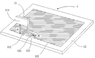
- FIG. 2 is a schematic view of an antenna device according to an embodiment of the present invention.
- FIG. 3 is a diagram showing an actual measurement of a voltage standing-wave ratio of the antenna device according to an embodiment of the present invention when resonated at 1575.42 MHz.
- FIG. 4 is a schematic view of an antenna device according to another embodiment of the present invention.
- the antenna device 1 in an embodiment of the present invention is an inverted F antenna applied in GPS.
- the antenna device 1 includes an antenna 11 disposed on a printed circuit board 12 .
- a radiation portion 111 of the antenna 11 is spaced by a suitable distance from the printed circuit board 12 , and a feed portion 112 of the antenna 11 extends downwardly from the radiation portion 111 to electrically connect a signal feed point 121 on the printed circuit board 12 .
- a conductive wire 123 is disposed on the printed circuit board 12 .
- the conductive wire 123 is, for example, a printed trace directly formed on the printed circuit board 12 , and extending externally from the signal feed point 121 to electrically connect a ground plane 122 on the printed circuit board 12 .
- the ground plane 122 is, for example, a short pad.
- the distance dl between the radiation portion 111 of the antenna 11 and the ground plane of the printed circuit board 12 is at least 2 mm.
- the length d 2 of the conductive wire 123 formed by the printed trace is preferably between 2 mm and 5 mm, and the width of the conductive wire 123 is preferably between 0.25 mm and 0.5 mm.
- the length of the conductive wire 123 is concerned, if the length d 2 of the conductive wire 123 is less than 2 mm, the signal energy on the antenna 11 is directly conducted into the ground plane 122 . If the length d 2 of the conductive wire 123 is greater than 5 mm, the loss of the signal energy on the antenna 11 may occur, and the volume of the antenna is increased, which further influences the performance of the antenna device 1 .
- the antenna device 1 in this embodiment is an inverted F antenna for GPS.
- the radiation portion 111 of the antenna 11 forms a plane substantially perpendicular to the printed circuit board 12 .
- the feed portion 112 of the antenna 11 may be mounted on the signal feed point 121 of the circuit board 12 by a surface mounting technology (SMT), and meanwhile, may be embedded by insert-molding into an antenna pedestal (not shown) made of a plastic. Then one end of the antenna pedestal is fixed on the printed circuit board 12 by heat stacking.
- SMT surface mounting technology
- the radiation portion 111 of the new-type antenna 11 of the present invention is located at the upper left edge of the printed circuit board 12 of a hand-held antenna device 1 (e.g., a smart phone), and is 21 mm ⁇ 3 mm ⁇ 5 mm in volume, which is much smaller than that of the common patch antenna (15 mm ⁇ 15 mm ⁇ 5 mm in volume) applied in the GPS.
- the material of antenna 11 of the antenna device 1 in this embodiment is, for example, phosphor bronze, which has a more stable characteristic and lower cost than the material of the conventional chip antenna used in the GPS.
- FIG. 3 is a diagram showing an actual measurement of the voltage standing-wave ratio of the antenna device 1 in the above embodiment when resonated at 1575.42 MHz. It can be seen from FIG. 3 that, in the actual measurement, the center frequency of the antenna device 1 is 1575.42 MHz. Therefore, the actual measurement data in the above embodiment is in consistent with the operating frequency range of the GPS.
- FIG. 4 shows an antenna device 1 according to another embodiment of the present invention.
- the antenna device 1 is also applied in an inverted F antenna of the GPS.
- the antenna device 1 includes an antenna 11 disposed on a printed circuit board 12 .
- a radiation portion 111 of the antenna 11 is spaced by a suitable distance from the printed circuit board 12 , and a feed portion 112 of the antenna 11 extends downwardly from the radiation portion 111 to electrically connect a signal feed point 121 of the printed circuit board 12 .
- a conductive wire 123 is disposed on the printed circuit board 12 .
- the conductive wire 123 is, for example, a printed trace directly formed on the printed circuit board 12 , and extending externally from the signal feed point 121 to electrically connect a ground plane 122 on the printed circuit board 12 .
- the ground plane 122 is, for example, a short pad.
- the antenna device of the present invention is the GPS antenna.
- the antenna device of the present invention may also be applied in a wireless LAN (WiFi) antenna or a Bluetooth communication antenna.
- the antenna device of the present invention may be, but not limited to, a PDA mobile phone, a smart phone, a satellite navigator, or a PDA.
- the ground effect of the conventional inverted F antenna can also be achieved without disposing an additional ground portion to ground the antenna.
- the ground portion of the antenna is not disposed in the antenna device of the present invention, and thus the hardware space for electronic device is effectively reduced, thereby meeting the requirements on low cost and miniaturization.
- the antenna body is mounted on the circuit board by a surface mounting technology (SMT), and meanwhile, the antenna body is embedded by insert-molding into the antenna pedestal made of a plastic. Then, one end of the antenna pedestal is fixed on the printed circuit board by heat stacking.
- SMT surface mounting technology
- the members can be fixed more stably, and a better resistance control can be achieved.
- ground plane is included in the circuit board in the above embodiments, the ground plane may be a standalone component separate from the circuit board in some other embodiments of the present invention.
Landscapes
- Engineering & Computer Science (AREA)
- Computer Hardware Design (AREA)
- General Engineering & Computer Science (AREA)
- Computer Networks & Wireless Communication (AREA)
- Waveguide Aerials (AREA)
- Support Of Aerials (AREA)
- Details Of Aerials (AREA)
Abstract
Description
- This application claims the priority benefit of Taiwan application serial no. 96144308, filed on Nov. 22, 2007. The entirety of the above-mentioned patent application is hereby incorporated by reference herein and made a part of this specification.
- 1. Field of the Invention
- The present invention generally relates to an antenna device, in particular, to a planar inverted F antenna (PIFA) device applied in a global positioning system (GPS).
- 2. Description of Related Art
- Nowadays, communities of people have growing demands for wireless communication, and various types of wireless communication devices have been developed, including smart phones, multimedia players, PDAs, and satellite navigators using the global positioning system (GPS). Electronic devices provided with the wireless transmission function are improved complying with the design notion of “thin, light, short, and small”, so as to meet the requirements of daily use electronic products.
- The conventional GPS antenna applied in the wireless device is usually a chip antenna, a patch antenna, or a planar inverted F antenna. Among them, the chip antenna has a higher price and cost since the manufacturing process of the chip is more complicated than other metal antennas. The patch antenna or the planar inverted F antenna requires a large area, and occupies an effective radiation area on the circuit board, thus greatly lowering the space utilization of the circuit board. In the planar inverted F antenna, the metal radiator thereof is spaced by a suitable distance from the circuit board, and the energy is resonated between the antenna and the circuit board and is radiated in the form of a linearly polarized wave. The architecture of the patch antenna mainly is the chip antenna, and includes a signal feed point, utilizes a ground plane as an energy resonance surface, and radiates in the form of a circularly polarized wave. This antenna has a higher directivity, but requires a larger antenna area and a higher price, and is not applicable to the mobile mode of mobile phones. In addition, the conventional GPS antenna usually contacts the signal feed point or short pad through a pogo-pin or a leaf spring, thus resulting in the difficulties in controlling the resistance.
-
FIG. 1 shows a structure of a conventional planar inverted F antenna. The planar invertedF antenna 3 includes aplanar radiator 31, afeed portion 32, and aground portion 33. Theradiator 31 is disposed above thecircuit board 4, and theground portion 33 extends downwardly from theradiator 31 to electrically connect theground plane 42 on thecircuit board 4 through a ground leaf spring (not shown). And, thefeed portion 32 extends downwardly from a position approximately in the middle of theradiator 31 to electrically connect thesignal feed point 41. Therefore, in the conventional planar invertedF antenna 3, thesignal feed point 41 and theground plane 42 of thecircuit board 4 are not connected. - In the above conventional art, an extending space for the
ground portion 33 of theantenna 3 must be provided on thecircuit board 4, so as to achieve a better antenna performance. However, under the requirements of improved functions and miniaturization of the hand-held electronic devices, it is difficult to provide extra room for the planar inverted F antenna to ground downwardly. And, as for the GPS antenna, when the planar inverted F antenna is not grounded, even if the size of the radiator is greatly increased, the required frequency cannot be achieved, which not only causes a higher cost, but also goes against the requirements of the miniaturization of the electronic devices. - Accordingly, the present invention is directed to an antenna device, which includes a ground plane, a circuit board, an antenna, and a conductive wire. The circuit board includes a signal feed point, and the antenna includes a radiation portion and a feed portion extending externally from the radiation portion. The feed portion is electrically connected to the signal feed point, and the conductive wire is disposed on the circuit board and electrically connected to the ground plane and the signal feed point. The ground plane may be a part of the circuit board or separate from the circuit board.
- According to an embodiment of the present invention, the conductive wire is, for example, a printed trace formed on the circuit board. The length of the conductive wire is preferably between 2 mm and 5 mm, and the width of the conductive wire is preferably between 0.25 mm and 0.5 mm. Moreover, the distance between the radiation portion and the ground plane of the antenna is at least 2 mm.
- In the antenna device according to an embodiment of the present invention, the radiation portion of the antenna forms a plane substantially parallel to the circuit board or substantially perpendicular to the circuit board.
- In the antenna device according to an embodiment of the present invention, the antenna is fixed by insert-molding to an antenna pedestal, and mounted on the circuit board by a surface mounting technology (SMT).
- Moreover, the antenna device of the present invention may be applied not only in a GPS antenna, but also in a wireless LAN (WiFi) antenna or a Bluetooth communication antenna.
- According to another embodiment of the present invention, another antenna device is provided. The antenna device includes a ground plane, a signal feed point, an antenna, and a conductive wire. The antenna includes a radiation portion and a feed portion which extends from the radiation portion and is electrically connected to the signal feed point. The conductive wire is electrically connected to the ground plane and the signal feed point.
- In an embodiment of the present invention, the radiation portion has a plane and the plane of the radiation portion is either substantially perpendicular to the ground plane or substantially parallel to the ground plane.
- In the present invention, since the printed trace formed on the circuit board is electrically connected to the signal feed point and the ground plane on the circuit board, the ground effect of the conventional inverted F antenna can also be achieved without disposing an additional ground portion to ground the antenna. Compared with the conventional art, the ground portion of the antenna is not required by the antenna device of the present invention, and thus the hardware space for the electronic device is effectively reduced, thereby meeting the requirements of lower cost and miniaturization.
- The accompanying drawings are included to provide a further understanding of the invention, and are incorporated in and constitute a part of this specification. The drawings illustrate embodiments of the invention and, together with the description, serve to explain the principles of the invention.
-
FIG. 1 is a schematic view of a conventional planar inverted F antenna. -
FIG. 2 is a schematic view of an antenna device according to an embodiment of the present invention. -
FIG. 3 is a diagram showing an actual measurement of a voltage standing-wave ratio of the antenna device according to an embodiment of the present invention when resonated at 1575.42 MHz. -
FIG. 4 is a schematic view of an antenna device according to another embodiment of the present invention. - Reference will now be made in detail to the present embodiments of the invention, examples of which are illustrated in the accompanying drawings. Wherever possible, the same reference numbers are used in the drawings and the description to refer to the same or like parts.
- Referring to
FIG. 2 , theantenna device 1 in an embodiment of the present invention is an inverted F antenna applied in GPS. Theantenna device 1 includes anantenna 11 disposed on a printedcircuit board 12. Aradiation portion 111 of theantenna 11 is spaced by a suitable distance from the printedcircuit board 12, and afeed portion 112 of theantenna 11 extends downwardly from theradiation portion 111 to electrically connect asignal feed point 121 on the printedcircuit board 12. - In this embodiment, a
conductive wire 123 is disposed on the printedcircuit board 12. Theconductive wire 123 is, for example, a printed trace directly formed on the printedcircuit board 12, and extending externally from thesignal feed point 121 to electrically connect aground plane 122 on the printedcircuit board 12. Theground plane 122 is, for example, a short pad. - In order to achieve better performance of the
antenna device 1, the distance dl between theradiation portion 111 of theantenna 11 and the ground plane of the printedcircuit board 12 is at least 2 mm. Moreover, the length d2 of theconductive wire 123 formed by the printed trace is preferably between 2 mm and 5 mm, and the width of theconductive wire 123 is preferably between 0.25 mm and 0.5 mm. As far as the length of theconductive wire 123 is concerned, if the length d2 of theconductive wire 123 is less than 2 mm, the signal energy on theantenna 11 is directly conducted into theground plane 122. If the length d2 of theconductive wire 123 is greater than 5 mm, the loss of the signal energy on theantenna 11 may occur, and the volume of the antenna is increased, which further influences the performance of theantenna device 1. - The
antenna device 1 in this embodiment is an inverted F antenna for GPS. Theradiation portion 111 of theantenna 11 forms a plane substantially perpendicular to the printedcircuit board 12. In this embodiment, in order to achieve a better effect of fixing theantenna 11 on the printedcircuit board 12, thefeed portion 112 of theantenna 11 may be mounted on thesignal feed point 121 of thecircuit board 12 by a surface mounting technology (SMT), and meanwhile, may be embedded by insert-molding into an antenna pedestal (not shown) made of a plastic. Then one end of the antenna pedestal is fixed on the printedcircuit board 12 by heat stacking. Moreover, in the above embodiment, theradiation portion 111 of the new-type antenna 11 of the present invention is located at the upper left edge of the printedcircuit board 12 of a hand-held antenna device 1 (e.g., a smart phone), and is 21 mm×3 mm×5 mm in volume, which is much smaller than that of the common patch antenna (15 mm×15 mm×5 mm in volume) applied in the GPS. Moreover, the material ofantenna 11 of theantenna device 1 in this embodiment is, for example, phosphor bronze, which has a more stable characteristic and lower cost than the material of the conventional chip antenna used in the GPS. - Referring to
FIG. 3 , for the performance and the actual operating frequency range of the antenna, it is known that the operating frequency range of the GPS is 1575.42±2 MHz.FIG. 3 is a diagram showing an actual measurement of the voltage standing-wave ratio of theantenna device 1 in the above embodiment when resonated at 1575.42 MHz. It can be seen fromFIG. 3 that, in the actual measurement, the center frequency of theantenna device 1 is 1575.42 MHz. Therefore, the actual measurement data in the above embodiment is in consistent with the operating frequency range of the GPS. -
FIG. 4 shows anantenna device 1 according to another embodiment of the present invention. In this embodiment, theantenna device 1 is also applied in an inverted F antenna of the GPS. Theantenna device 1 includes anantenna 11 disposed on a printedcircuit board 12. Aradiation portion 111 of theantenna 11 is spaced by a suitable distance from the printedcircuit board 12, and afeed portion 112 of theantenna 11 extends downwardly from theradiation portion 111 to electrically connect asignal feed point 121 of the printedcircuit board 12. - A
conductive wire 123 is disposed on the printedcircuit board 12. Theconductive wire 123 is, for example, a printed trace directly formed on the printedcircuit board 12, and extending externally from thesignal feed point 121 to electrically connect aground plane 122 on the printedcircuit board 12. Theground plane 122 is, for example, a short pad. - The difference between this embodiment and the above embodiment lies in that the plane formed by the
radiation portion 111 of theantenna 11 in this embodiment is substantially parallel to the printed circuit board. Other conditions and methods in the two embodiments are substantially the same, and will not be repeated herein. - In the above embodiment, the antenna device of the present invention is the GPS antenna. However, the antenna device of the present invention may also be applied in a wireless LAN (WiFi) antenna or a Bluetooth communication antenna. The antenna device of the present invention may be, but not limited to, a PDA mobile phone, a smart phone, a satellite navigator, or a PDA.
- In the present invention, since the printed trace formed on the circuit board is electrically connected to the signal feed point and the ground plane on the circuit board, the ground effect of the conventional inverted F antenna can also be achieved without disposing an additional ground portion to ground the antenna. Compared with the conventional art, the ground portion of the antenna is not disposed in the antenna device of the present invention, and thus the hardware space for electronic device is effectively reduced, thereby meeting the requirements on low cost and miniaturization.
- Moreover, the antenna body is mounted on the circuit board by a surface mounting technology (SMT), and meanwhile, the antenna body is embedded by insert-molding into the antenna pedestal made of a plastic. Then, one end of the antenna pedestal is fixed on the printed circuit board by heat stacking. Thus, different from the conventional GPS antenna which contacts the signal feed point or short pad through the pogo-pin or leaf spring, in the present invention, the members can be fixed more stably, and a better resistance control can be achieved.
- Although the ground plane is included in the circuit board in the above embodiments, the ground plane may be a standalone component separate from the circuit board in some other embodiments of the present invention.
- It will be apparent to those skilled in the art that various modifications and variations can be made to the structure of the present invention without departing from the scope or spirit of the invention. In view of the foregoing, it is intended that the present invention cover modifications and variations of this invention provided they fall within the scope of the following claims and their equivalents.
Claims (25)
Applications Claiming Priority (3)
| Application Number | Priority Date | Filing Date | Title |
|---|---|---|---|
| TW96144308 | 2007-11-22 | ||
| TW96144308A | 2007-11-22 | ||
| TW096144308A TWI388088B (en) | 2007-11-22 | 2007-11-22 | Antenna device |
Publications (2)
| Publication Number | Publication Date |
|---|---|
| US20090135067A1 true US20090135067A1 (en) | 2009-05-28 |
| US7714786B2 US7714786B2 (en) | 2010-05-11 |
Family
ID=39267876
Family Applications (1)
| Application Number | Title | Priority Date | Filing Date |
|---|---|---|---|
| US11/969,227 Active US7714786B2 (en) | 2007-11-22 | 2008-01-04 | Antenna device |
Country Status (4)
| Country | Link |
|---|---|
| US (1) | US7714786B2 (en) |
| EP (1) | EP2063485A1 (en) |
| JP (1) | JP2009130925A (en) |
| TW (1) | TWI388088B (en) |
Cited By (5)
| Publication number | Priority date | Publication date | Assignee | Title |
|---|---|---|---|---|
| US20090195478A1 (en) * | 2008-02-04 | 2009-08-06 | Quanta Computer Inc. | Low-Profile Antenna |
| CN108051996A (en) * | 2018-01-17 | 2018-05-18 | 出门问问信息科技有限公司 | A kind of substrate and smartwatch |
| US20190293728A1 (en) * | 2018-03-24 | 2019-09-26 | Melexis Technologies Sa | Magnetic sensor component and assembly |
| CN114824765A (en) * | 2022-06-23 | 2022-07-29 | 深圳华大北斗科技股份有限公司 | Dual-frequency GNSS antenna |
| US11543466B2 (en) | 2018-03-24 | 2023-01-03 | Melexis Technologies Sa | Magnetic sensor component and assembly |
Families Citing this family (7)
| Publication number | Priority date | Publication date | Assignee | Title |
|---|---|---|---|---|
| CN101719584B (en) * | 2009-12-24 | 2013-08-28 | 华为终端有限公司 | Reconfigurable mobile phone built-in antenna and implementation method thereof |
| CN201616506U (en) * | 2010-03-26 | 2010-10-27 | 华为终端有限公司 | Mobile communication antenna equipment and mobile communication terminal equipment |
| CN102646864A (en) * | 2011-02-18 | 2012-08-22 | 英华达(上海)科技有限公司 | Flexible multiple antenna |
| CN106299638A (en) * | 2016-05-20 | 2017-01-04 | 北京小鸟听听科技有限公司 | A kind of for surface-pasted antenna and design and production method thereof |
| TWI626791B (en) * | 2016-08-31 | 2018-06-11 | 宏碁股份有限公司 | Wearable communication device |
| CN107808995B (en) * | 2016-09-08 | 2020-07-14 | 宏碁股份有限公司 | Wearable communication device |
| CN207338628U (en) * | 2017-08-18 | 2018-05-08 | 咏业科技股份有限公司 | The antenna assembly of particular radiation field pattern can be produced |
Citations (7)
| Publication number | Priority date | Publication date | Assignee | Title |
|---|---|---|---|---|
| US6239765B1 (en) * | 1999-02-27 | 2001-05-29 | Rangestar Wireless, Inc. | Asymmetric dipole antenna assembly |
| US20030174092A1 (en) * | 2002-03-15 | 2003-09-18 | Sullivan Jonathan Lee | Planar inverted-F antenna including a matching network having transmission line stubs and capacitor/inductor tank circuits |
| US20040066334A1 (en) * | 2002-10-08 | 2004-04-08 | Wistron Neweb Corporation | Multifrequency inverted-F antenna |
| US20040070548A1 (en) * | 2002-09-09 | 2004-04-15 | Cake Brian Victor | Physically small antenna elements and antennas based thereon |
| US20040140938A1 (en) * | 2002-09-20 | 2004-07-22 | Kadambi Govind Rangaswamy | Compact, low profile, single feed, multi-band, printed antenna |
| US20040169606A1 (en) * | 2002-11-28 | 2004-09-02 | Kyocera Corporation | Surface-mount type antenna and antenna apparatus |
| US20050093752A1 (en) * | 2003-10-31 | 2005-05-05 | Ping-Xi Cheng | Antenna set for mobile devices |
Family Cites Families (5)
| Publication number | Priority date | Publication date | Assignee | Title |
|---|---|---|---|---|
| JP2004015500A (en) * | 2002-06-07 | 2004-01-15 | Nec Tokin Corp | Antenna element and antenna device |
| TW583783B (en) * | 2003-04-17 | 2004-04-11 | Htc Corp | Perpendicularly-oriented inverted F antenna |
| DE602004031989D1 (en) | 2003-12-25 | 2011-05-05 | Mitsubishi Materials Corp | Antenna device and communication device |
| JP2006319767A (en) * | 2005-05-13 | 2006-11-24 | Sony Corp | Flat antenna |
| CN100592572C (en) * | 2005-06-10 | 2010-02-24 | 鸿富锦精密工业(深圳)有限公司 | Dual-frequency antenna |
-
2007
- 2007-11-22 TW TW096144308A patent/TWI388088B/en active
-
2008
- 2008-01-04 US US11/969,227 patent/US7714786B2/en active Active
- 2008-01-16 EP EP08250214A patent/EP2063485A1/en not_active Ceased
- 2008-01-16 JP JP2008006540A patent/JP2009130925A/en active Pending
Patent Citations (8)
| Publication number | Priority date | Publication date | Assignee | Title |
|---|---|---|---|---|
| US6239765B1 (en) * | 1999-02-27 | 2001-05-29 | Rangestar Wireless, Inc. | Asymmetric dipole antenna assembly |
| US20030174092A1 (en) * | 2002-03-15 | 2003-09-18 | Sullivan Jonathan Lee | Planar inverted-F antenna including a matching network having transmission line stubs and capacitor/inductor tank circuits |
| US20040070548A1 (en) * | 2002-09-09 | 2004-04-15 | Cake Brian Victor | Physically small antenna elements and antennas based thereon |
| US20040140938A1 (en) * | 2002-09-20 | 2004-07-22 | Kadambi Govind Rangaswamy | Compact, low profile, single feed, multi-band, printed antenna |
| US20040066334A1 (en) * | 2002-10-08 | 2004-04-08 | Wistron Neweb Corporation | Multifrequency inverted-F antenna |
| US20060250309A1 (en) * | 2002-10-08 | 2006-11-09 | Wistron Neweb Corporation | Multifrequency inverted-F antenna |
| US20040169606A1 (en) * | 2002-11-28 | 2004-09-02 | Kyocera Corporation | Surface-mount type antenna and antenna apparatus |
| US20050093752A1 (en) * | 2003-10-31 | 2005-05-05 | Ping-Xi Cheng | Antenna set for mobile devices |
Cited By (7)
| Publication number | Priority date | Publication date | Assignee | Title |
|---|---|---|---|---|
| US20090195478A1 (en) * | 2008-02-04 | 2009-08-06 | Quanta Computer Inc. | Low-Profile Antenna |
| CN108051996A (en) * | 2018-01-17 | 2018-05-18 | 出门问问信息科技有限公司 | A kind of substrate and smartwatch |
| US20190293728A1 (en) * | 2018-03-24 | 2019-09-26 | Melexis Technologies Sa | Magnetic sensor component and assembly |
| US11067645B2 (en) * | 2018-03-24 | 2021-07-20 | Melexis Technologies Sa | Magnetic sensor component and assembly |
| US11474165B2 (en) | 2018-03-24 | 2022-10-18 | Melexis Technologies Sa | Magnetic sensor component and assembly |
| US11543466B2 (en) | 2018-03-24 | 2023-01-03 | Melexis Technologies Sa | Magnetic sensor component and assembly |
| CN114824765A (en) * | 2022-06-23 | 2022-07-29 | 深圳华大北斗科技股份有限公司 | Dual-frequency GNSS antenna |
Also Published As
| Publication number | Publication date |
|---|---|
| EP2063485A1 (en) | 2009-05-27 |
| JP2009130925A (en) | 2009-06-11 |
| TWI388088B (en) | 2013-03-01 |
| US7714786B2 (en) | 2010-05-11 |
| TW200924293A (en) | 2009-06-01 |
Similar Documents
| Publication | Publication Date | Title |
|---|---|---|
| US7714786B2 (en) | Antenna device | |
| US10680314B2 (en) | Antenna device of mobile terminal | |
| US7161543B2 (en) | Antenna set for mobile devices | |
| US9502750B2 (en) | Electronic device with reduced emitted radiation during loaded antenna operating conditions | |
| US9070985B2 (en) | Mobile device and antenna structure therein | |
| US7821470B2 (en) | Antenna arrangement | |
| US7486245B2 (en) | Mobile terminal with plural antennas | |
| US7969371B2 (en) | Small monopole antenna having loop element included feeder | |
| US6492952B1 (en) | Antenna device, a communication device including such an antenna device and a method of operating the communication device | |
| US20100289702A1 (en) | Dual-band antenna and portable wireless communication device using the same | |
| US8299972B2 (en) | Antenna for portable device | |
| CN101442152B (en) | Antenna device | |
| US20170025759A1 (en) | Mobile device | |
| US20100177005A1 (en) | Multi-Band Antenna | |
| US20110074647A1 (en) | Antenna module | |
| US20110156960A1 (en) | Antenna module | |
| US7696942B2 (en) | Slot antenna | |
| KR20100030025A (en) | Small-sized patch antenna | |
| US8681054B2 (en) | PIFA/monopole hybrid antenna and mobile communications device having the same | |
| US7439921B2 (en) | Chip antenna apparatus for receiving global positioning system signals | |
| US20130099978A1 (en) | Internal printed antenna | |
| CN212848804U (en) | Circularly polarized antenna and electronic equipment | |
| US7710332B2 (en) | Mobile communications device with a compact-sized three-dimensional antenna | |
| EP3053220B1 (en) | Electronic device with pifa type antenna and wireless signal transmitting/receiving device thereof | |
| Lin et al. | A λ/2 loop antenna for GPS application in mini-laptop |
Legal Events
| Date | Code | Title | Description |
|---|---|---|---|
| AS | Assignment |
Owner name: HIGH TECH COMPUTER, CORP., TAIWAN Free format text: ASSIGNMENT OF ASSIGNORS INTEREST;ASSIGNORS:CHEN, MIN-CHE;CHEN, KUO-CHENG;WANG, CHING-SUNG;REEL/FRAME:020380/0003 Effective date: 20071231 Owner name: HIGH TECH COMPUTER, CORP.,TAIWAN Free format text: ASSIGNMENT OF ASSIGNORS INTEREST;ASSIGNORS:CHEN, MIN-CHE;CHEN, KUO-CHENG;WANG, CHING-SUNG;REEL/FRAME:020380/0003 Effective date: 20071231 |
|
| AS | Assignment |
Owner name: HTC CORPORATION,TAIWAN Free format text: ASSIGNMENT OF ASSIGNORS INTEREST;ASSIGNOR:HIGH TECH COMPUTER CORPORATION;REEL/FRAME:023972/0542 Effective date: 20090318 |
|
| STCF | Information on status: patent grant |
Free format text: PATENTED CASE |
|
| FPAY | Fee payment |
Year of fee payment: 4 |
|
| MAFP | Maintenance fee payment |
Free format text: PAYMENT OF MAINTENANCE FEE, 8TH YEAR, LARGE ENTITY (ORIGINAL EVENT CODE: M1552) Year of fee payment: 8 |
|
| MAFP | Maintenance fee payment |
Free format text: PAYMENT OF MAINTENANCE FEE, 12TH YEAR, LARGE ENTITY (ORIGINAL EVENT CODE: M1553); ENTITY STATUS OF PATENT OWNER: LARGE ENTITY Year of fee payment: 12 |