US20060292786A1 - Semiconductor constructions, and methods of forming semiconductor constructions - Google Patents
Semiconductor constructions, and methods of forming semiconductor constructions Download PDFInfo
- Publication number
- US20060292786A1 US20060292786A1 US11/167,011 US16701105A US2006292786A1 US 20060292786 A1 US20060292786 A1 US 20060292786A1 US 16701105 A US16701105 A US 16701105A US 2006292786 A1 US2006292786 A1 US 2006292786A1
- Authority
- US
- United States
- Prior art keywords
- composition
- construction
- copper
- over
- atomic percent
- Prior art date
- Legal status (The legal status is an assumption and is not a legal conclusion. Google has not performed a legal analysis and makes no representation as to the accuracy of the status listed.)
- Granted
Links
- 238000010276 construction Methods 0.000 title claims abstract description 76
- 239000004065 semiconductor Substances 0.000 title claims abstract description 72
- 238000000034 method Methods 0.000 title claims abstract description 39
- 239000000463 material Substances 0.000 claims abstract description 222
- 239000000203 mixture Substances 0.000 claims abstract description 155
- RYGMFSIKBFXOCR-UHFFFAOYSA-N Copper Chemical compound [Cu] RYGMFSIKBFXOCR-UHFFFAOYSA-N 0.000 claims abstract description 91
- 229910052802 copper Inorganic materials 0.000 claims abstract description 91
- 239000010949 copper Substances 0.000 claims abstract description 91
- 229910052715 tantalum Inorganic materials 0.000 claims abstract description 83
- GUVRBAGPIYLISA-UHFFFAOYSA-N tantalum atom Chemical compound [Ta] GUVRBAGPIYLISA-UHFFFAOYSA-N 0.000 claims abstract description 62
- 229910052741 iridium Inorganic materials 0.000 claims abstract description 51
- 239000000758 substrate Substances 0.000 claims description 32
- 229910052751 metal Inorganic materials 0.000 claims description 29
- 239000002184 metal Substances 0.000 claims description 29
- BASFCYQUMIYNBI-UHFFFAOYSA-N platinum Chemical compound [Pt] BASFCYQUMIYNBI-UHFFFAOYSA-N 0.000 claims description 28
- 239000003990 capacitor Substances 0.000 claims description 23
- KDLHZDBZIXYQEI-UHFFFAOYSA-N Palladium Chemical compound [Pd] KDLHZDBZIXYQEI-UHFFFAOYSA-N 0.000 claims description 20
- VYPSYNLAJGMNEJ-UHFFFAOYSA-N Silicium dioxide Chemical compound O=[Si]=O VYPSYNLAJGMNEJ-UHFFFAOYSA-N 0.000 claims description 18
- 238000005498 polishing Methods 0.000 claims description 16
- 229910052697 platinum Inorganic materials 0.000 claims description 14
- 229910021421 monocrystalline silicon Inorganic materials 0.000 claims description 12
- 229910000510 noble metal Inorganic materials 0.000 claims description 12
- 229910052710 silicon Inorganic materials 0.000 claims description 11
- 239000010703 silicon Substances 0.000 claims description 11
- 229910052763 palladium Inorganic materials 0.000 claims description 10
- BQCADISMDOOEFD-UHFFFAOYSA-N Silver Chemical compound [Ag] BQCADISMDOOEFD-UHFFFAOYSA-N 0.000 claims description 9
- 238000009713 electroplating Methods 0.000 claims description 9
- PCHJSUWPFVWCPO-UHFFFAOYSA-N gold Chemical compound [Au] PCHJSUWPFVWCPO-UHFFFAOYSA-N 0.000 claims description 9
- 229910052737 gold Inorganic materials 0.000 claims description 9
- 239000010931 gold Substances 0.000 claims description 9
- 235000012239 silicon dioxide Nutrition 0.000 claims description 9
- 239000000377 silicon dioxide Substances 0.000 claims description 9
- 229910052709 silver Inorganic materials 0.000 claims description 9
- 239000004332 silver Substances 0.000 claims description 9
- 230000015572 biosynthetic process Effects 0.000 claims description 8
- 239000003989 dielectric material Substances 0.000 claims description 8
- 239000005380 borophosphosilicate glass Substances 0.000 claims description 5
- 239000005360 phosphosilicate glass Substances 0.000 claims description 5
- 238000007747 plating Methods 0.000 claims 1
- 230000004888 barrier function Effects 0.000 abstract description 44
- GKOZUEZYRPOHIO-UHFFFAOYSA-N iridium atom Chemical compound [Ir] GKOZUEZYRPOHIO-UHFFFAOYSA-N 0.000 abstract description 32
- 238000009792 diffusion process Methods 0.000 abstract description 23
- 238000012545 processing Methods 0.000 description 44
- 230000015654 memory Effects 0.000 description 29
- 239000012634 fragment Substances 0.000 description 27
- NJPPVKZQTLUDBO-UHFFFAOYSA-N novaluron Chemical compound C1=C(Cl)C(OC(F)(F)C(OC(F)(F)F)F)=CC=C1NC(=O)NC(=O)C1=C(F)C=CC=C1F NJPPVKZQTLUDBO-UHFFFAOYSA-N 0.000 description 21
- MZLGASXMSKOWSE-UHFFFAOYSA-N tantalum nitride Chemical compound [Ta]#N MZLGASXMSKOWSE-UHFFFAOYSA-N 0.000 description 17
- 239000004020 conductor Substances 0.000 description 15
- KJTLSVCANCCWHF-UHFFFAOYSA-N Ruthenium Chemical compound [Ru] KJTLSVCANCCWHF-UHFFFAOYSA-N 0.000 description 7
- 238000010586 diagram Methods 0.000 description 7
- 150000002739 metals Chemical class 0.000 description 7
- 229910052707 ruthenium Inorganic materials 0.000 description 7
- XUIMIQQOPSSXEZ-UHFFFAOYSA-N Silicon Chemical compound [Si] XUIMIQQOPSSXEZ-UHFFFAOYSA-N 0.000 description 6
- 238000004891 communication Methods 0.000 description 5
- QVGXLLKOCUKJST-UHFFFAOYSA-N atomic oxygen Chemical compound [O] QVGXLLKOCUKJST-UHFFFAOYSA-N 0.000 description 4
- 230000008901 benefit Effects 0.000 description 4
- 238000002425 crystallisation Methods 0.000 description 4
- 230000008025 crystallization Effects 0.000 description 4
- 238000004519 manufacturing process Methods 0.000 description 4
- 239000001301 oxygen Substances 0.000 description 4
- 229910052760 oxygen Inorganic materials 0.000 description 4
- 229920002120 photoresistant polymer Polymers 0.000 description 4
- 229910000575 Ir alloy Inorganic materials 0.000 description 3
- 229910052581 Si3N4 Inorganic materials 0.000 description 3
- 229910001362 Ta alloys Inorganic materials 0.000 description 3
- 230000010354 integration Effects 0.000 description 3
- BPUBBGLMJRNUCC-UHFFFAOYSA-N oxygen(2-);tantalum(5+) Chemical compound [O-2].[O-2].[O-2].[O-2].[O-2].[Ta+5].[Ta+5] BPUBBGLMJRNUCC-UHFFFAOYSA-N 0.000 description 3
- 230000001681 protective effect Effects 0.000 description 3
- HQVNEWCFYHHQES-UHFFFAOYSA-N silicon nitride Chemical compound N12[Si]34N5[Si]62N3[Si]51N64 HQVNEWCFYHHQES-UHFFFAOYSA-N 0.000 description 3
- 229910045601 alloy Inorganic materials 0.000 description 2
- 239000000956 alloy Substances 0.000 description 2
- 238000000429 assembly Methods 0.000 description 2
- 230000000712 assembly Effects 0.000 description 2
- 230000007423 decrease Effects 0.000 description 2
- 238000000151 deposition Methods 0.000 description 2
- 239000002019 doping agent Substances 0.000 description 2
- 238000002955 isolation Methods 0.000 description 2
- 150000002736 metal compounds Chemical class 0.000 description 2
- 230000005012 migration Effects 0.000 description 2
- 238000013508 migration Methods 0.000 description 2
- 230000008520 organization Effects 0.000 description 2
- 238000004886 process control Methods 0.000 description 2
- 125000006850 spacer group Chemical group 0.000 description 2
- PBCFLUZVCVVTBY-UHFFFAOYSA-N tantalum pentoxide Inorganic materials O=[Ta](=O)O[Ta](=O)=O PBCFLUZVCVVTBY-UHFFFAOYSA-N 0.000 description 2
- XKRFYHLGVUSROY-UHFFFAOYSA-N argon Substances [Ar] XKRFYHLGVUSROY-UHFFFAOYSA-N 0.000 description 1
- 229910052786 argon Inorganic materials 0.000 description 1
- -1 argon ions Chemical class 0.000 description 1
- 238000003491 array Methods 0.000 description 1
- 230000009286 beneficial effect Effects 0.000 description 1
- 230000001351 cycling effect Effects 0.000 description 1
- 230000008021 deposition Effects 0.000 description 1
- 230000009977 dual effect Effects 0.000 description 1
- 230000000694 effects Effects 0.000 description 1
- 238000005530 etching Methods 0.000 description 1
- 230000006870 function Effects 0.000 description 1
- 238000011065 in-situ storage Methods 0.000 description 1
- 230000003993 interaction Effects 0.000 description 1
- 229910021645 metal ion Inorganic materials 0.000 description 1
- 239000007769 metal material Substances 0.000 description 1
- 238000001465 metallisation Methods 0.000 description 1
- 238000012986 modification Methods 0.000 description 1
- 230000004048 modification Effects 0.000 description 1
- TWNQGVIAIRXVLR-UHFFFAOYSA-N oxo(oxoalumanyloxy)alumane Chemical compound O=[Al]O[Al]=O TWNQGVIAIRXVLR-UHFFFAOYSA-N 0.000 description 1
- 238000000059 patterning Methods 0.000 description 1
- 230000002093 peripheral effect Effects 0.000 description 1
- 239000012466 permeate Substances 0.000 description 1
- 230000000704 physical effect Effects 0.000 description 1
- 230000008569 process Effects 0.000 description 1
- 238000005389 semiconductor device fabrication Methods 0.000 description 1
- 239000000126 substance Substances 0.000 description 1
- 229910001936 tantalum oxide Inorganic materials 0.000 description 1
Images


Classifications
-
- H—ELECTRICITY
- H10—SEMICONDUCTOR DEVICES; ELECTRIC SOLID-STATE DEVICES NOT OTHERWISE PROVIDED FOR
- H10B—ELECTRONIC MEMORY DEVICES
- H10B12/00—Dynamic random access memory [DRAM] devices
- H10B12/01—Manufacture or treatment
- H10B12/02—Manufacture or treatment for one transistor one-capacitor [1T-1C] memory cells
- H10B12/03—Making the capacitor or connections thereto
- H10B12/033—Making the capacitor or connections thereto the capacitor extending over the transistor
- H10B12/0335—Making a connection between the transistor and the capacitor, e.g. plug
-
- H—ELECTRICITY
- H01—ELECTRIC ELEMENTS
- H01L—SEMICONDUCTOR DEVICES NOT COVERED BY CLASS H10
- H01L21/00—Processes or apparatus adapted for the manufacture or treatment of semiconductor or solid state devices or of parts thereof
- H01L21/02—Manufacture or treatment of semiconductor devices or of parts thereof
- H01L21/04—Manufacture or treatment of semiconductor devices or of parts thereof the devices having potential barriers, e.g. a PN junction, depletion layer or carrier concentration layer
- H01L21/18—Manufacture or treatment of semiconductor devices or of parts thereof the devices having potential barriers, e.g. a PN junction, depletion layer or carrier concentration layer the devices having semiconductor bodies comprising elements of Group IV of the Periodic Table or AIIIBV compounds with or without impurities, e.g. doping materials
- H01L21/28—Manufacture of electrodes on semiconductor bodies using processes or apparatus not provided for in groups H01L21/20 - H01L21/268
- H01L21/283—Deposition of conductive or insulating materials for electrodes conducting electric current
- H01L21/285—Deposition of conductive or insulating materials for electrodes conducting electric current from a gas or vapour, e.g. condensation
- H01L21/28506—Deposition of conductive or insulating materials for electrodes conducting electric current from a gas or vapour, e.g. condensation of conductive layers
- H01L21/28512—Deposition of conductive or insulating materials for electrodes conducting electric current from a gas or vapour, e.g. condensation of conductive layers on semiconductor bodies comprising elements of Group IV of the Periodic Table
- H01L21/28568—Deposition of conductive or insulating materials for electrodes conducting electric current from a gas or vapour, e.g. condensation of conductive layers on semiconductor bodies comprising elements of Group IV of the Periodic Table the conductive layers comprising transition metals
-
- H—ELECTRICITY
- H01—ELECTRIC ELEMENTS
- H01L—SEMICONDUCTOR DEVICES NOT COVERED BY CLASS H10
- H01L21/00—Processes or apparatus adapted for the manufacture or treatment of semiconductor or solid state devices or of parts thereof
- H01L21/70—Manufacture or treatment of devices consisting of a plurality of solid state components formed in or on a common substrate or of parts thereof; Manufacture of integrated circuit devices or of parts thereof
- H01L21/71—Manufacture of specific parts of devices defined in group H01L21/70
- H01L21/768—Applying interconnections to be used for carrying current between separate components within a device comprising conductors and dielectrics
- H01L21/76838—Applying interconnections to be used for carrying current between separate components within a device comprising conductors and dielectrics characterised by the formation and the after-treatment of the conductors
- H01L21/76841—Barrier, adhesion or liner layers
- H01L21/76843—Barrier, adhesion or liner layers formed in openings in a dielectric
- H01L21/76844—Bottomless liners
-
- H—ELECTRICITY
- H01—ELECTRIC ELEMENTS
- H01L—SEMICONDUCTOR DEVICES NOT COVERED BY CLASS H10
- H01L21/00—Processes or apparatus adapted for the manufacture or treatment of semiconductor or solid state devices or of parts thereof
- H01L21/70—Manufacture or treatment of devices consisting of a plurality of solid state components formed in or on a common substrate or of parts thereof; Manufacture of integrated circuit devices or of parts thereof
- H01L21/71—Manufacture of specific parts of devices defined in group H01L21/70
- H01L21/768—Applying interconnections to be used for carrying current between separate components within a device comprising conductors and dielectrics
- H01L21/76838—Applying interconnections to be used for carrying current between separate components within a device comprising conductors and dielectrics characterised by the formation and the after-treatment of the conductors
- H01L21/76841—Barrier, adhesion or liner layers
- H01L21/7687—Thin films associated with contacts of capacitors
-
- H—ELECTRICITY
- H01—ELECTRIC ELEMENTS
- H01L—SEMICONDUCTOR DEVICES NOT COVERED BY CLASS H10
- H01L21/00—Processes or apparatus adapted for the manufacture or treatment of semiconductor or solid state devices or of parts thereof
- H01L21/70—Manufacture or treatment of devices consisting of a plurality of solid state components formed in or on a common substrate or of parts thereof; Manufacture of integrated circuit devices or of parts thereof
- H01L21/71—Manufacture of specific parts of devices defined in group H01L21/70
- H01L21/768—Applying interconnections to be used for carrying current between separate components within a device comprising conductors and dielectrics
- H01L21/76838—Applying interconnections to be used for carrying current between separate components within a device comprising conductors and dielectrics characterised by the formation and the after-treatment of the conductors
- H01L21/76841—Barrier, adhesion or liner layers
- H01L21/76871—Layers specifically deposited to enhance or enable the nucleation of further layers, i.e. seed layers
- H01L21/76873—Layers specifically deposited to enhance or enable the nucleation of further layers, i.e. seed layers for electroplating
-
- H—ELECTRICITY
- H01—ELECTRIC ELEMENTS
- H01L—SEMICONDUCTOR DEVICES NOT COVERED BY CLASS H10
- H01L21/00—Processes or apparatus adapted for the manufacture or treatment of semiconductor or solid state devices or of parts thereof
- H01L21/70—Manufacture or treatment of devices consisting of a plurality of solid state components formed in or on a common substrate or of parts thereof; Manufacture of integrated circuit devices or of parts thereof
- H01L21/71—Manufacture of specific parts of devices defined in group H01L21/70
- H01L21/768—Applying interconnections to be used for carrying current between separate components within a device comprising conductors and dielectrics
- H01L21/76838—Applying interconnections to be used for carrying current between separate components within a device comprising conductors and dielectrics characterised by the formation and the after-treatment of the conductors
- H01L21/76877—Filling of holes, grooves or trenches, e.g. vias, with conductive material
- H01L21/76879—Filling of holes, grooves or trenches, e.g. vias, with conductive material by selective deposition of conductive material in the vias, e.g. selective C.V.D. on semiconductor material, plating
-
- H—ELECTRICITY
- H01—ELECTRIC ELEMENTS
- H01L—SEMICONDUCTOR DEVICES NOT COVERED BY CLASS H10
- H01L23/00—Details of semiconductor or other solid state devices
- H01L23/48—Arrangements for conducting electric current to or from the solid state body in operation, e.g. leads, terminal arrangements ; Selection of materials therefor
- H01L23/482—Arrangements for conducting electric current to or from the solid state body in operation, e.g. leads, terminal arrangements ; Selection of materials therefor consisting of lead-in layers inseparably applied to the semiconductor body (electrodes)
- H01L23/485—Arrangements for conducting electric current to or from the solid state body in operation, e.g. leads, terminal arrangements ; Selection of materials therefor consisting of lead-in layers inseparably applied to the semiconductor body (electrodes) consisting of layered constructions comprising conductive layers and insulating layers, e.g. planar contacts
-
- H—ELECTRICITY
- H01—ELECTRIC ELEMENTS
- H01L—SEMICONDUCTOR DEVICES NOT COVERED BY CLASS H10
- H01L23/00—Details of semiconductor or other solid state devices
- H01L23/52—Arrangements for conducting electric current within the device in operation from one component to another, i.e. interconnections, e.g. wires, lead frames
- H01L23/522—Arrangements for conducting electric current within the device in operation from one component to another, i.e. interconnections, e.g. wires, lead frames including external interconnections consisting of a multilayer structure of conductive and insulating layers inseparably formed on the semiconductor body
- H01L23/532—Arrangements for conducting electric current within the device in operation from one component to another, i.e. interconnections, e.g. wires, lead frames including external interconnections consisting of a multilayer structure of conductive and insulating layers inseparably formed on the semiconductor body characterised by the materials
- H01L23/53204—Conductive materials
- H01L23/53209—Conductive materials based on metals, e.g. alloys, metal silicides
- H01L23/53228—Conductive materials based on metals, e.g. alloys, metal silicides the principal metal being copper
- H01L23/53238—Additional layers associated with copper layers, e.g. adhesion, barrier, cladding layers
-
- H01L28/65—
-
- H01L28/75—
-
- H—ELECTRICITY
- H01—ELECTRIC ELEMENTS
- H01L—SEMICONDUCTOR DEVICES NOT COVERED BY CLASS H10
- H01L2924/00—Indexing scheme for arrangements or methods for connecting or disconnecting semiconductor or solid-state bodies as covered by H01L24/00
- H01L2924/0001—Technical content checked by a classifier
- H01L2924/0002—Not covered by any one of groups H01L24/00, H01L24/00 and H01L2224/00
Definitions
- the invention pertains to semiconductor constructions and to methods of forming semiconductor constructions.
- barrier layers are provided to impede, and preferably prevent, migration of various materials therethrough.
- copper diffusion can be a problem when utilizing copper interconnects, and accordingly barrier materials are provided proximate the copper interconnects to preclude copper diffusion.
- a common copper-barrier material is tantalum nitride.
- tantalum nitride it is difficult to deposit copper directly on tantalum nitride, and accordingly the tantalum nitride will typically be utilized as part of a tantalum nitride/tantalum bi-layer.
- the tantalum of the bi-layer is provided as a material onto which copper can be readily deposited.
- the tantalum is utilized in bi-layers with tantalum nitride, rather than alone, because pure tantalum is a poor barrier to copper diffusion. Pure tantalum can contain crystallization-induced columnar textures. Copper can permeate the tantalum along boundaries between adjacent columnar grains.
- the copper barrier materials create numerous difficulties as copper line size decreases.
- the copper diffusion barrier begins to limit the amount by which a copper line can be shrunk.
- barrier materials comprising tantalum there can be a challenge in that the columnar tantalum texture can create difficulties in forming the film to be 25 ⁇ or less in thickness.
- tantalum nitride/ruthenium has been studied as a bi-layer material for utilization with copper.
- the tantalum nitride is an amorphous material which precludes copper diffusion
- the ruthenium is a seed material for growing the copper.
- the tantalum nitride/ruthenium bi-layer is utilized instead of a single barrier layer in that the ruthenium lacks suitable barrier properties and the tantalum nitride lacks suitable properties for growing copper thereon. Accordingly, the tantalum nitride is utilized as a barrier to copper diffusion and the ruthenium is utilized to provide a substrate onto which copper can be grown.
- a continuing goal in semiconductor device fabrication is to decrease the dimension of circuit elements in order to increase the level of integration.
- it is desired to develop new barrier materials suitable for alleviating copper diffusion.
- Barrier materials can have other applications besides the above-discussed applications of alleviating copper diffusion.
- barrier materials can be utilized to alleviate silicon diffusion, oxygen diffusion, and/or diffusion of numerous other materials.
- metal-insulator-metal (MIM) capacitors are formed over conductively-doped semiconductor pedestals (such as, for example, conductively-doped silicon pedestals).
- the electrode of the capacitor closest to the conductively-doped semiconductor pedestal i.e., the lower electrode
- the electrode of the capacitor closest to the conductively-doped semiconductor pedestal i.e., the lower electrode
- a diffusion barrier material can be provided between the lower capacitor electrode and the conductively-doped semiconductor pedestal in order to alleviate, and preferably prevent, oxygen diffusion from the high-k dielectric through the lower electrode and into the conductively-doped semiconductor.
- barrier material including, for example, tantalum nitride.
- there can be difficulties associated with the various prior art barrier materials and it would therefore be desirable to develop new materials which can be utilized for barriers between a capacitor electrode and a conductively-doped
- barrier materials including, for example, between conductively-doped diffusion regions and conductive interconnects. It would be desirable to develop new barrier materials that are suitable for utilization in a wide variety of applications.
- the invention includes a semiconductor construction comprising a composition that contains both Ir and Ta.
- the composition can be provided between a copper-containing material and an electrically insulative material.
- the composition can be provided between a capacitor electrode comprising one or more of gold, silver, palladium and platinum, and a semiconductor material (such as, for example, conductively-doped silicon).
- the composition can be provided between a conductive interconnect and a conductively-doped diffusion region formed within a monocrystalline semiconductor material.
- the composition containing Ir and Ta can, in some applications, consist essentially of iridium and tantalum. In such applications, the composition can contain the tantalum to a concentration of from about 40 atomic % to about 70 atomic %, and in exemplary applications will contain the tantalum to a concentration of from about 50 atomic % to about 65 atomic %.
- the invention includes a method of forming a semiconductor construction.
- a semiconductor substrate is provided, and such substrate has an electrically insulative material thereover.
- a composition containing Ir and Ta is formed over the electrically insulative material, and a copper-containing material is formed over the composition.
- the invention includes another method of forming a semiconductor construction.
- a semiconductor material is provided.
- a first composition is formed over the semiconductor material, with the first composition comprising Ta and Ir.
- a second composition is formed over the first composition, with the second composition comprising one or more of gold, silver, palladium, and platinum.
- FIG. 1 is a diagrammatic, cross-sectional view of a semiconductor wafer fragment at a preliminary processing stage of an exemplary aspect of the present invention.
- FIG. 2 is a view of the FIG. 1 wafer fragment shown at a processing stage subsequent to that of FIG. 1 .
- FIG. 3 is a view of the FIG. 1 wafer fragment shown at a processing stage subsequent to that of FIG. 2 .
- FIG. 4 is a view of the FIG. 1 wafer fragment shown at a processing stage subsequent to that of FIG. 3 .
- FIG. 5 is a view of the FIG. 1 wafer fragment shown at a processing stage subsequent to that of FIG. 4 .
- FIG. 6 is a top view of a region of a semiconductor wafer comprising the fragment of FIG. 5 .
- the fragment of FIG. 5 is shown along the line 5 - 5 of FIG. 6 .
- FIG. 7 is a view of the FIG. 1 wafer fragment shown at a processing stage subsequent to that of FIG. 3 in accordance with a second aspect of the invention.
- FIG. 8 is a view of the FIG. 1 wafer fragment shown at a processing stage subsequent of that of FIG. 7 .
- FIG. 9 is a diagrammatic, cross-sectional view of a semiconductor wafer fragment shown at a preliminary processing stage of another aspect of the present invention.
- FIG. 10 is a view of the FIG. 9 wafer fragment shown at a processing stage subsequent to that of FIG. 9 .
- FIG. 11 is a diagrammatic, cross-sectional view of a semiconductor wafer fragment shown at a preliminary processing stage of yet another aspect of the present invention.
- FIG. 12 is a view of the FIG. 11 wafer fragment shown at a processing stage subsequent to that of FIG. 11 .
- FIG. 13 is a view of the FIG. 11 wafer fragment shown at a processing stage subsequent to that of FIG. 12 .
- FIG. 14 is a view of the FIG. 11 wafer fragment shown at a processing stage subsequent to that of FIG. 13 .
- FIG. 15 is a view of the FIG. 11 wafer fragment shown at a processing stage subsequent to that of FIG. 12 in accordance with yet another aspect of the present invention.
- FIG. 16 is a view of the FIG. 11 wafer fragment shown at a processing stage subsequent to that of FIG. 15 .
- FIG. 17 is a view of the FIG. 11 wafer fragment shown at a processing stage subsequent to that of FIG. 16 .
- FIG. 18 is a view of the FIG. 11 wafer fragment shown at a processing stage subsequent to that of FIG. 15 in accordance with yet another aspect of the present invention.
- FIG. 19 is a view of the FIG. 11 wafer fragment shown at a processing stage subsequent to that of FIG. 18 .
- FIG. 20 is a diagrammatic, cross-sectional view of a semiconductor wafer fragment at a preliminary processing stage of another exemplary aspect of the present invention.
- FIG. 21 is a view of the FIG. 20 wafer fragment shown at a processing stage subsequent to that of FIG. 20 .
- FIG. 22 is a view of the FIG. 20 wafer fragment shown at a processing stage subsequent to that of FIG. 21 .
- FIG. 23 is a view of the FIG. 20 wafer fragment shown at a processing stage subsequent to that of FIG. 20 in accordance with another aspect of the invention.
- FIG. 24 is a view of the FIG. 20 wafer fragment shown at a processing stage subsequent to that of FIG. 23 .
- FIG. 25 is a diagrammatic, cross-sectional view of a semiconductor wafer fragment illustrating an exemplary aspect of the present invention.
- FIG. 26 is a diagrammatic view of a computer illustrating an exemplary application of the present invention.
- FIG. 27 is a block diagram showing particular features of the motherboard of the FIG. 26 computer.
- FIG. 28 is a high level block diagram of an electronic system according to an exemplary aspect of the present invention.
- FIG. 29 is a simplified block diagram of an exemplary memory device according to an aspect of the present invention.
- the invention includes methods for utilizing compositions containing iridium and tantalum in semiconductor constructions.
- a thin layer for instance, a layer having a thickness of from about 10 ⁇ to about 200 ⁇ , and in exemplary aspects from about 15 ⁇ to about 50 ⁇
- the layer can consist essentially of, or consist of iridium and tantalum, and can contain from about 40 atomic % to about 70 atomic % tantalum in some aspects, and in particular aspects can contain from about 50 atomic % to about 65 atomic % tantalum.
- the alloy can be Ir 45 Ta 55 .
- the iridium/tantalum material can not only be utilized as a barrier material, but can also be utilized as a substrate for electroplating of a desired metal thereover.
- the iridium/tantalum material can be utilized as a substrate for electroplating copper thereover.
- the iridium/tantalum material can overcome problems associated with prior art barrier materials, such as, for example, the problems discussed in the “Background” section of this disclosure regarding tantalum nitride/tantalum bi-layers and tantalum nitride/ruthenium bi-layers.
- the present invention can comprise a significant departure from conventional bi-layer barrier materials.
- the present invention utilizes a single material which can have suitable barrier properties, and yet can also provide a substrate to which copper can be adhered.
- the single material is a composition comprising-both iridium and tantalum.
- Such composition can have amorphous properties which preclude diffusion of copper therethrough, and yet can have suitable properties for electroplating copper directly thereon, or for retaining a copper seed onto which copper is subsequently electroplated.
- Iridium/tantalum alloys can have very high crystallization temperatures, which can be beneficial since the amorphous forms of the alloys will generally have better barrier properties than the crystalline forms.
- An exemplary iridium/tantalum alloy is Ir 45 Ta 55 , which has a crystallization temperature of about 1010° C.
- iridium/tantalum materials can also have good adhesion to dielectric materials, such as, for example, low-k dielectrics like borophosphosilicate glass (BPSG), phosphosilicate glass (PSG), silicon dioxide, etc.
- dielectric materials such as, for example, low-k dielectrics like borophosphosilicate glass (BPSG), phosphosilicate glass (PSG), silicon dioxide, etc.
- FIGS. 1-6 An exemplary aspect of the invention is described with reference to FIGS. 1-6 .
- a semiconductor wafer construction 10 is illustrated in cross-sectional view.
- Such construction comprises a semiconductor substrate 12 having an insulative material 14 thereover.
- Substrate 12 can, for example, comprise, consist essentially of, or consist of monocrystalline silicon lightly-background doped with p-type dopant.
- semiconductor substrate and “semiconductor substrate” are defined to mean any construction comprising semiconductive material, including, but not limited to, bulk semiconductive materials such as a semiconductive wafer (either alone or in assemblies comprising other materials thereon), and semiconductive material layers (either alone or in assemblies comprising other materials).
- substrate refers to any supporting structure, including, but not limited to, the semiconductive substrates described above.
- Insulative material 14 can comprise any suitable electrically insulative composition, including, for example, one or more of BPSG, PSG and silicon dioxide.
- trenches 16 and 18 are formed into insulative material 14 .
- the trenches can be formed with any suitable processing, including, for example, utilization of a photolithographically patterned photoresist mask to define the locations of the trenches, followed by etching into the defined locations to form the trenches and subsequent removal of the photoresist mask.
- a layer 20 is formed over insulative material 14 and within trenches 16 and 18 .
- Layer 20 can comprise a composition containing iridium and tantalum, and in particular aspects will consist essentially of, or consist of iridium and tantalum.
- the layer can be formed to a thickness of from about 10 ⁇ to about 200 ⁇ , and in particular aspects will be formed very thin, such as, for example, to a thickness of from about 15 ⁇ to about 50 ⁇ , or even from about 15 ⁇ to about 30 ⁇ .
- composition of layer 20 consists essentially of iridium and tantalum, or consists of iridium and tantalum
- such composition can contain the tantalum to a concentration of from about 40 atomic % to about 70 atomic %, and in particular aspects can contain the tantalum to a concentration to from about 50 atomic % to about 65 atomic %.
- the composition can consist essentially of, or consist of Ir 45 Ta 55 .
- the layer 20 can be formed utilizing any suitable processing, but preferably will have amorphous properties, and accordingly will be formed at a temperature of less than the crystallization temperature of the iridium/tantalum material therein.
- the copper-containing layer 22 can comprise, consist essentially of, or consist of copper.
- Copper-containing material 22 can be formed over layer 20 utilizing any suitable processing.
- the copper layer 22 can be directly electroplated onto the iridium/tantalum-containing material 20 .
- a copper-containing seed can be first formed over layer 20 , and subsequently the layer 22 can be electroplated onto the copper-containing seed.
- copper-containing material 22 is provided to completely fill trenches 16 and 18 . It is to be understood, however, that the invention encompasses other aspects (not shown) in which the copper-containing material only partially fills the trenches.
- the layer 20 can be considered to form a liner which completely lines the peripheries of the trenches, and the copper-containing material 22 can be considered to be formed directly on the liner.
- copper-containing material 22 is separated from the insulative material by only the liner.
- the iridium/tantalum-containing composition of layer 20 physically contacts both the copper-containing material 22 and the insulative material 14 .
- FIGS. 1-4 can be utilized during formation of any level of metal layer, with various metal layer levels being typically referred to as Metal I, Metal II, Metal III, etc.
- FIGS. 20 and 21 illustrate a typical Metal I or Metal N (where N is an integer greater than 1) metal level that can be formed in accordance with some aspects of the invention.
- the fragment 10 is shown at a processing stage subsequent to FIG. 4 .
- Copper-containing material 22 and iridium/tantalum-containing layer 20 are removed from over insulative material 14 by planarization to form a planarized upper surface 23 extending across insulative material 14 , layer 20 and material 22 .
- the planarization can comprise, for example, chemical-mechanical polishing.
- the chemical-mechanical polishing can stop on an uppermost surface of layer 14 , or can penetrate partially into layer 14 .
- compositions tend to be relatively soft.
- the compositions can be relatively easily removed by chemical-mechanical polishing.
- FIG. 6 shows a top view of the construction of FIG. 5 , and shows that the copper-containing material 22 and barrier layer 20 can form lines extending across a region of the semiconductor substrate. Such lines can be considered a shape of the copper-containing material 22 at the processing stage of FIGS. 5 and 6 , and it is to be understood that the material 22 can also be formed in other shapes including, for example, pedestals, pads, etc. for various applications in semiconductor constructions.
- the semiconductor construction 10 at the processing stage of FIGS. 5 and 6 can correspond to any suitable level of semiconductor fabrication.
- semiconductor fabrication typically involves formation of multiple levels of circuitry over and within a semiconductor substrate.
- levels of circuitry include circuit devices, and include various wiring levels, with the wiring levels frequently being referred to as level I, level II, level III, etc.
- the structures 12 and 14 of FIGS. 1-6 can have various levels of semiconductor devices (not shown) formed therein, or can be at a preliminary stage of semiconductor fabrication in which no levels of circuitry have yet been formed.
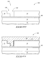
- FIGS. 1-6 Although the invention described with reference to FIGS. 1-6 has the copper-containing material formed over layer 20 prior to chemical-mechanical polishing of layer 20 , it is to be understood that the invention encompasses other aspects in which the chemical-mechanical polishing (or other planarization process) occurs before formation of the copper-containing material. Such aspect is described with reference to FIGS. 7 and 8 .
- construction 10 is shown at a processing stage subsequent to that of FIG. 3 , and specifically is shown after chemical-mechanical polishing (or other suitable planarization) has been utilized to remove layer 20 from over insulative material 14 and thereby form a planarized upper surface 25 .
- the insulative material 14 can be considered to comprise segments 26 proximate the trenches 16 and 18 , and the planarization can be considered to remove layer 20 from over such segments.
- the planarization can also remove some of the insulative material 14 associated with the segments, but regardless the planarization has removed layer 20 from over the segments.
- the shown aspect of the invention forms two trenches and three segments proximate the trenches, but it is to be understood that the invention encompasses other aspects in which other numbers of trenches and segments are formed.
- copper-containing material 22 is formed within trenches 16 and 18 and over layer 20 .
- the copper-containing material 22 can be formed selectively onto layer 20 by electroplating material 22 onto layer 20 ; either directly on layer 20 , or onto a copper-seed which is provided onto layer 20 prior to the electroplating. Such forms the copper-containing material 22 only within trenches 16 and 18 , and not over the segments of insulative material 14 between the trenches.
- copper-containing material 22 can be formed by other methods which form the copper-containing material 22 both within the trenches and over the insulative material 14 between the trenches, and subsequently the copper-containing material can be patterned to leave the material only within the trenches. Such patterning can be accomplished by planarization of the copper-containing material (for instance, chemical-mechanical polishing), or by any other suitable method.
- barrier layer 20 can be used both as a barrier layer and as a substrate for copper growth, and thus can replace the bi-layer constructions traditionally utilized to provide a copper barrier and a substrate for copper growth (for example, the tantalum nitride/tantalum bi-layers or tantalum nitride/ruthenium bi-layers).
- the barrier layer 20 can be formed to be much thinner than bi-layer constructions, while still achieving the same benefits as are obtained with the bi-layer constructions. Thus, the barrier layer 20 can be more suitable for high levels of integration than the bi-layer constructions.
- FIGS. 9 and 10 Another aspect of the invention is described with reference to FIGS. 9 and 10 .
- similar numbering will be used as was utilized above in describing the aspect of FIGS. 1-8 , where appropriate.
- a semiconductor construction 50 comprises a substrate 12 .
- Such substrate can, for example, comprise, consist essentially of, or consist of monocrystalline silicon lightly-doped with appropriate background-type dopant.
- a trenched isolation region 52 extends within the substrate.
- the trenched isolation region can comprise any suitable electrically insulative composition or combination of compositions, and in particular aspects will comprise, consist essentially of, or consist of silicon dioxide.
- a transistor device 54 is supported by substrate 12 .
- the transistor device comprises a transistor gate 56 and a pair of source/drain regions 58 and 60 .
- the transistor gate 56 comprises a gate dielectric 62 , a conductive gate region 64 , and an electrically insulative cap 66 .
- the gate dielectric 62 can comprise any suitable composition or combination of compositions, and in particular aspects will comprise, consist essentially of, or consist of silicon dioxide.
- the conductive gate region 64 can comprise any suitable composition or combination of compositions, and in particular aspects will comprise one or more of various metals, metal compounds, and conductively-doped semiconductor materials (such as, for example, conductively-doped silicon).
- the insulative cap 66 can comprise any suitable composition or combination of compositions, and in particular aspects will comprise one or both of silicon dioxide and silicon nitride.
- Source/drain regions 58 and 60 are conductively-doped diffusion regions extending into substrate 12 .
- substrate 12 can comprise monocrystalline silicon
- source/drain regions 58 and 60 can comprise p-type doped regions and/or n-type doped regions extending into the monocrystalline silicon.
- Sidewall spacers 68 are along opposing sidewalls of gate 56 .
- the sidewall spacers can comprise any suitable composition or combination of compositions, and in particular aspects will comprise one or both of silicon dioxide and silicon nitride.
- Insulative material 70 is over substrate 12 and transistor device 54 .
- Insulative material 70 can comprise any suitable composition or combination of compositions, and in particular aspects will comprise one or more of BPSG, PSG and silicon dioxide.
- Conductive pedestal 72 can comprise any suitable composition or combination of compositions, and in particular aspects will comprise one or more of various metals, metal compounds, and conductively-doped semiconductor material (with an exemplary conductively-doped semiconductor material being conductively-doped silicon).
- Planar surface 73 extends across pedestal 72 and insulative material 70 .
- Planar surface 73 can be formed by, for example, chemical-mechanical polishing.
- Barrier layer 80 is formed over surface 73 .
- Barrier layer 80 can comprise iridium and tantalum, and can have identical compositions and thicknesses as the layer 20 discussed above with reference to FIG. 3 .
- a capacitor stack 82 is formed over layer 80 .
- the capacitor stack comprises a first capacitor electrode 84 , a dielectric material 86 , and a second capacitor electrode 88 .
- the first and second capacitor electrodes can comprise any suitable electrically conductive material or combination of materials, including, for example, various metals, metal compositions, and conductively-doped semiconductor materials.
- the capacitor stack can be considered to have a first composition 84 , second composition 86 , and third composition 88 ; with the first and third compositions being capacitively coupled to one another.
- the capacitor construction 82 will correspond to a metal-insulator-metal construction, and accordingly electrodes 84 and 88 will comprise various metals.
- Such metals can be noble metals or near noble metals, and in particular aspects can comprise, consist essentially of, or consist of one or more of gold, silver, platinum, and palladium.
- both of the electrodes 84 and 88 can consist essentially of, or consist of platinum or palladium.
- the dielectric material 86 can be any suitable composition or combination of compositions, and in particular aspects can comprise, consist essentially of, or consist of one or more of silicon dioxide, silicon nitride, and various high-k dielectric materials (such as, for example, tantalum oxide and aluminum oxide).
- the composition 80 comprising tantalum and iridium separates the capacitor construction 82 from the conductively-doped semiconductor material of pedestal 72 .
- the lower electrode 84 is directly against the layer 80 comprising tantalum and iridium
- the pedestal 72 is also directly against the layer 80 comprising tantalum and iridium.
- the dielectric 86 can comprise a substance that can migrate through lower electrode 84 , and which is blocked by layer 80 from reaching materials underlying electrode 84 .
- dielectric material 86 can comprise tantalum pentoxide
- lower electrode 84 can comprise platinum
- pedestal 72 can comprise conductively-doped semiconductor material.
- oxygen from the tantalum pentoxide can migrate through the platinum of layer 84 .
- the iridium/tantalum composition of layer 80 can be a barrier to prevent such oxygen from reaching the conductively-doped semiconductor material of pedestal 72 .
- the tantalum/iridium composition of layer 80 can function as a barrier to prevent migration of materials from capacitor construction 82 into conductively-doped semiconductor material (such as, for example, conductively-doped silicon) of pedestal 72 .
- An advantage of using iridium/tantalum of layer 80 as a barrier can be that the electrode 84 can be electroplated onto material 80 .
- Another advantage of utilizing the iridium/tantalum material as a barrier is that such can provide a thinner barrier material than prior art barrier materials.
- the transistor 54 and capacitor stack 82 can together form a dynamic random access memory (DRAM) unit cell.
- the source/drain region 58 can be connected to a bitline 90 in some aspects of the invention so that the DRAM unit cell can be incorporated into a DRAM array.
- Capacitor constructions formed utilizing methodology of the present invention can have numerous geometries, including, for example, the planar geometry of FIG. 10 , a pedestal configuration, or a container capacitor geometry of the type discussed below with reference to FIG. 22 .
- FIGS. 11-19 Additional aspects of the invention are discussed with reference to FIGS. 11-19 .
- similar number will be used as was utilized above in describing the aspects of FIGS. 1-6 , where appropriate.
- the construction 100 comprises a substrate 12 having an insulative material 14 thereover.
- the construction also comprises a conductively-doped diffusion region 102 extending into substrate 12 .
- the conductively-doped diffusion region is an exemplary conductive node, and it is to be understood that other conductive nodes can be provided, with other exemplary conductive nodes being metal-containing materials.
- an opening 104 is formed to extend through insulative material 14 and to the diffusion region 102 .
- the opening can be formed by any suitable processing, including, for example, formation of a photolithographically patterned photoresist mask over insulative material 14 to define the location of the opening, an etch through material 14 to form the opening, and subsequent removal of the photoresist mask.
- a layer 106 is formed along the bottom of opening 104 .
- the layer 106 can comprise, consist essentially of, or consist of Ir/Ta, and can have a thickness and composition identical to the thicknesses and compositions discussed above for layer 20 of FIG. 3 .
- Conductive material 108 can comprise, consist essentially of, or consist of conductively-doped semiconductor material, various metals and/or various metal compositions. Exemplary metals that can be utilized in material 108 are copper, noble metals and near noble metals; with exemplary noble metals and near noble metals including gold, silver, platinum and palladium.
- the material 108 can be referred to as a second composition to distinguish such material from the first composition of layer 106 .
- the conductive material 108 directly contacts an uppermost surface of layer 106
- layer 106 directly contacts an uppermost surface of substrate 12 .
- substrate 12 can comprise, consist essentially of, or consist of monocrystalline silicon, and the layer 106 comprising tantalum/iridium can thus be in direct physical contact with such monocrystalline silicon. Also, the layer 106 can be in direct physical contact with material 108 .
- the conductive material 108 can ultimately be formed into a conductive pedestal contained within opening 104 by, for example, chemical-mechanical polishing to remove layer 108 from over insulative material 104 while leaving the material 108 within the opening 104 .
- the conductive material 108 is shown entirely filling opening 104 , it is to be understood that the invention encompasses other aspects in which material 108 only partially fills opening 104 .
- FIG. 15 such shows construction 100 at a processing stage subsequent to FIG. 12 in accordance with another aspect of the invention.
- the layer 106 is shown to extend over an uppermost surface of insulative material 14 , as well as within opening 104 and along sidewalls of the opening.
- the construction of FIG. 16 can be considered to comprise segments 110 of insulative material 14 proximate opening 104 , and to comprise Ir/Ta-containing layer 106 extending over such segments.
- construction 100 is shown at a processing stage subsequent to FIG. 15 .
- Conductive material 108 has been formed over layer 106 and within opening 104 to fill the remainder of the opening.
- the conductive 108 also extends over segments 110 of material 14 .
- FIG. 17 shows a processing stage subsequent to FIG. 16 .
- Materials 106 and 108 have been subjected to planarization (such as, for example, chemical-mechanical polishing) to remove materials 106 and 108 from over segments 110 of insulative material 14 , and to thereby form a planarized upper surface 111 .
- the materials 106 and 108 thus form a conductive interconnect extending upwardly from diffusion region 102 to the upper surface 111 .
- FIG. 18 such shows construction 100 at a processing stage subsequent to that of FIG. 15 in accordance with another aspect of the invention. Specifically, the material 106 has been removed from over segments 110 , but left within opening 104 . Such removal can be accomplished by, for example, chemical-mechanical polishing.
- conductive material 108 is selectively formed on material 106 relative to insulative material 14 . Such can be accomplished by, for example, electroplating material 108 onto conductive material 106 .
- conductive material 108 can comprise any metal which can be electroplated onto material 106 ; which can include, for example, one or more of copper, platinum, palladium, gold and silver in various aspects of the invention.
- the conductive material 108 forms a conductive interconnect which can subsequently be utilized for connecting electrically conductive circuitry (not shown) with diffusion region 102 .
- FIGS. 20-24 show exemplary metal interconnects which can be formed in accordance with aspects of the present invention.
- the numbering utilized in FIGS. 20-24 is identical to that used in FIG. 4 , where appropriate.
- FIG. 20 shows a structure 150 comprising a metal layer 160 extending within insulative material 14 .
- the metal layer can correspond to any metal level, including, for example, a Metal I level, a Metal II level, a Metal III, level, etc.; and can be generally referred to as a Metal N level, where “N” is an integer.
- the metal layer 160 can comprise any suitable metal, and in some aspects can comprise, consist essentially of, or consist of copper. In such aspects, the layer can be formed against a Ta/Ir barrier material (not shown) of the type described previously in this disclosure.
- An opening 154 extends through material 14 and to an upper surface of metal layer 160 .
- the opening comprises a trench 156 extending in a direction orthogonal to the cross-sectional view of FIG. 20 , and a via 158 extending through the trench and connecting to layer 160 .
- the opening 154 is a typical opening utilized for damascene fabrication of metal layers associated with integrated circuitry, as will be recognized by persons of ordinary skill in the art.
- the Ta/Ir material 20 discussed previously is formed over an upper surface of material 14 and within opening 154 ; and copper-containing material 22 is formed over material 20 .
- the processing utilized to form materials 20 and 22 can be identical to methods discussed previously in this disclosure.
- materials 20 and 22 are polished from over the uppermost surface of material 14 , and left within opening 154 .
- the polishing can correspond to, for example, chemical-mechanical polishing.
- the materials 20 and 22 within the trench 156 of opening 154 form a metal line extending orthogonally to the line 160 .
- the line 160 can be a metal line at a level “N”, and the line formed within trench 156 can be at the level “N+1”.
- FIG. 22 has Ta/Ir material 20 at the interface between material 22 and the conductive material of line 160 .
- it can be desired for the conductive material 22 to directly contact the conductive material of line 160 .
- it can be desired to remove material 22 from the bottom of via 158 prior to forming material 22 within the via.
- FIG. 23 shows construction 150 at a processing stage subsequent to that of FIG. 20 , and shows material 20 formed within opening 154 and removed from the bottom of via 158 . Such removal can be accomplished by protecting portions of material 20 that are not at the bottom of via 158 with a protective mask (not shown), and then subjecting the material 20 at the bottom of via 158 to any suitable etch which removes the material 20 .
- the protective mask can then be removed to leave the structure of FIG. 23 .
- the structure of FIG. 23 can be formed by depositing material 20 in a manner which forms the material within trench 156 , but not along the bottom of via 158 .
- Another exemplary method of forming a structure having the FIG. 23 exposed material 160 at the bottom of via 158 is to use an in situ sputter etch (using for example, metal ions or argon ions), post deposition of the material 20 .
- the sputter etch can clear the material 20 from the bottom of the via while leaving the material along the sidewalls of the via 158 and trench 156 , and can be conducted without utilization of a protective mask.
- construction 150 is shown after material 22 is provided within opening 154 , and after polishing to remove materials 20 and 22 from over an uppermost surface material 14 (in other words, after processing analogous to that discussed above with reference to FIGS. 21 and 22 ).
- the construction of FIG. 24 has copper-containing material 22 directly contacting the conductive material of line 160 .
- FIG. 25 shows an exemplary container-type metal-insulator-metal capacitor which can be formed in accordance with aspects of the present invention.
- the capacitor is shown electrically connected with a transistor, and thus incorporated into a DRAM unit cell.
- the numbering utilized in FIG. 25 is identical to that utilized in FIG. 10 .
- FIG. 26 illustrates generally, by way of example but not by way of limitation, an embodiment of a computer system 400 according to an aspect of the present invention.
- Computer system 400 includes a monitor 401 or other communication output device, a keyboard 402 or other communication input device, and a motherboard 404 .
- Motherboard 404 can carry a microprocessor 406 or other data processing unit, and at least one memory device 408 .
- Memory device 408 can comprise various aspects of the invention described above, including, for example, the DRAM unit cell of FIG. 10 and/or that of FIG. 25 .
- Memory device 408 can comprise an array of memory cells, and such array can be coupled with addressing circuitry for accessing individual memory cells in the array.
- the memory cell array can be coupled to a read circuit for reading data from the memory cells.
- the addressing and read circuitry can be utilized for conveying information between memory device 408 and processor 406 . Such is illustrated in the block diagram of the motherboard 404 shown in FIG. 27 . In such block diagram, the addressing circuitry is illustrated as 410 and the read circuitry is illustrated as 412 .
- Various components of computer system 400 including processor 406 , can comprise one or more of the memory constructions described previously in this disclosure.
- Processor device 406 can correspond to a processor module, and associated memory utilized with the module can comprise teachings of the present invention.
- Memory device 408 can correspond to a memory module.
- SIMMs single in-line memory modules
- DIMMs dual in-line memory modules
- the memory device can be incorporated into any of a variety of designs which provide different methods of reading from and writing to memory cells of the device.
- One such method is the page mode operation.
- Page mode operations in a DRAM are defined by the method of accessing a row of a memory cell arrays and randomly accessing different columns of the array. Data stored at the row and column intersection can be read and output while that column is accessed.
- EDO extended data output
- Memory device 408 can comprise memory formed in accordance with one or more aspects of the present invention described above with reference to FIGS. 1-22 .
- FIG. 28 illustrates a simplified block diagram of a high-level organization of various embodiments of an exemplary electronic system 700 of the present invention.
- System 700 can correspond to, for example, a computer system, a process control system, or any other system that employs a processor and associated memory.
- Electronic system 700 has functional elements, including a processor or arithmetic/logic unit (ALU) 702 , a control unit 704 , a memory device unit 706 and an input/output (I/O) device 708 .
- ALU arithmetic/logic unit
- control unit 704 controls the a memory device unit 706
- I/O input/output
- electronic system 700 will have a native set of instructions that specify operations to be performed on data by the processor 702 and other interactions between the processor 702 , the memory device unit 706 and the I/O devices 708 .
- the control unit 704 coordinates all operations of the processor 702 , the memory device 706 and the I/O devices 708 by continuously cycling through a set of operations that cause instructions to be fetched from the memory device 706 and executed.
- the memory device 706 includes, but is not limited to, random access memory (RAM) devices, read-only memory (ROM) devices, and peripheral devices such as a floppy disk drive and a compact disk CD-ROM drive.
- RAM random access memory
- ROM read-only memory
- peripheral devices such as a floppy disk drive and a compact disk CD-ROM drive.
- FIG. 29 is a simplified block diagram of a high-level organization of various embodiments of an exemplary electronic system 800 .
- the system 800 includes a memory device 802 that has an array of memory cells 804 , address decoder 806 , row access circuitry 808 , column access circuitry 810 , read/write control circuitry 812 for controlling operations, and input/output circuitry 814 .
- the memory device 802 further includes power circuitry 816 , and sensors 820 , such as current sensors for determining whether a memory cell is in a low-threshold conducting state or in a high-threshold non-conducting state.
- the illustrated power circuitry 816 includes power supply circuitry 880 , circuitry 882 for providing a reference voltage, circuitry 884 for providing the first wordline with pulses, circuitry 886 for providing the second wordline with pulses, and circuitry 888 for providing the bitline with pulses.
- the system 800 also includes a processor 822 , or memory controller for memory accessing.
- the memory device 802 receives control signals from the processor 822 over wiring or metallization lines.
- the memory device 802 is used to store data which is accessed via I/O lines. It will be appreciated by those skilled in the art that additional circuitry and control signals can be provided, and that the memory device 802 has been simplified to help focus on the invention.
- At least one of the processor 822 or memory device 802 can include a memory construction of the type described previously in this disclosure.
- Applications for memory cells and other structures of the present invention can include electronic systems for use in memory modules, device drivers, power modules, communication modems, processor modules, and application-specific modules, and may include multilayer, multichip modules.
- Such circuitry can further be a subcomponent of a variety of electronic systems, such as a clock, a television, a cell phone, a personal computer, an automobile, an industrial control system, an aircraft, and others.
Landscapes
- Engineering & Computer Science (AREA)
- Power Engineering (AREA)
- Physics & Mathematics (AREA)
- Condensed Matter Physics & Semiconductors (AREA)
- General Physics & Mathematics (AREA)
- Computer Hardware Design (AREA)
- Microelectronics & Electronic Packaging (AREA)
- Manufacturing & Machinery (AREA)
- Chemical & Material Sciences (AREA)
- Crystallography & Structural Chemistry (AREA)
- Internal Circuitry In Semiconductor Integrated Circuit Devices (AREA)
Abstract
Description
- The invention pertains to semiconductor constructions and to methods of forming semiconductor constructions.
- It is frequently desired to utilize barrier layers in semiconductor constructions. The barrier layers are provided to impede, and preferably prevent, migration of various materials therethrough. For instance, copper diffusion can be a problem when utilizing copper interconnects, and accordingly barrier materials are provided proximate the copper interconnects to preclude copper diffusion. A common copper-barrier material is tantalum nitride. However, it is difficult to deposit copper directly on tantalum nitride, and accordingly the tantalum nitride will typically be utilized as part of a tantalum nitride/tantalum bi-layer. The tantalum of the bi-layer is provided as a material onto which copper can be readily deposited. The tantalum is utilized in bi-layers with tantalum nitride, rather than alone, because pure tantalum is a poor barrier to copper diffusion. Pure tantalum can contain crystallization-induced columnar textures. Copper can permeate the tantalum along boundaries between adjacent columnar grains.
- It is desired to form thinner copper lines as the level of integration increases, and copper barrier materials create numerous difficulties as copper line size decreases. For instance, it is typical to utilize a tantalum nitride/tantalum bi-layer having a thickness of from about 75 Å to about 150 Å, and there are numerous hardware/process control challenges to forming the bi-layer to be less than 50 Å. Thus, the copper diffusion barrier begins to limit the amount by which a copper line can be shrunk. Also, for barrier materials comprising tantalum there can be a challenge in that the columnar tantalum texture can create difficulties in forming the film to be 25 Å or less in thickness.
- There have been some attempts to utilize barrier materials other than the tantalum nitride/tantalum bi-layer. For instance, tantalum nitride/ruthenium has been studied as a bi-layer material for utilization with copper. The tantalum nitride is an amorphous material which precludes copper diffusion, and the ruthenium is a seed material for growing the copper. The tantalum nitride/ruthenium bi-layer is utilized instead of a single barrier layer in that the ruthenium lacks suitable barrier properties and the tantalum nitride lacks suitable properties for growing copper thereon. Accordingly, the tantalum nitride is utilized as a barrier to copper diffusion and the ruthenium is utilized to provide a substrate onto which copper can be grown.
- A continuing goal in semiconductor device fabrication is to decrease the dimension of circuit elements in order to increase the level of integration. Thus, it is desired to develop new barrier materials suitable for alleviating copper diffusion.
- Barrier materials can have other applications besides the above-discussed applications of alleviating copper diffusion. For instance, barrier materials can be utilized to alleviate silicon diffusion, oxygen diffusion, and/or diffusion of numerous other materials.
- In some applications, metal-insulator-metal (MIM) capacitors are formed over conductively-doped semiconductor pedestals (such as, for example, conductively-doped silicon pedestals). The electrode of the capacitor closest to the conductively-doped semiconductor pedestal (i.e., the lower electrode) can comprise a noble metal or near noble metal, such as, for example, gold, silver, platinum, palladium, etc. A diffusion barrier material can be provided between the lower capacitor electrode and the conductively-doped semiconductor pedestal in order to alleviate, and preferably prevent, oxygen diffusion from the high-k dielectric through the lower electrode and into the conductively-doped semiconductor. Various materials have been utilized for such barrier material, including, for example, tantalum nitride. However, there can be difficulties associated with the various prior art barrier materials, and it would therefore be desirable to develop new materials which can be utilized for barriers between a capacitor electrode and a conductively-doped semiconductor pedestal.
- Persons of ordinary skill in the art will also recognize that there are numerous other applications for barrier materials, including, for example, between conductively-doped diffusion regions and conductive interconnects. It would be desirable to develop new barrier materials that are suitable for utilization in a wide variety of applications.
- In one aspect, the invention includes a semiconductor construction comprising a composition that contains both Ir and Ta. In some embodiments, the composition can be provided between a copper-containing material and an electrically insulative material. In other embodiments, the composition can be provided between a capacitor electrode comprising one or more of gold, silver, palladium and platinum, and a semiconductor material (such as, for example, conductively-doped silicon). In yet other embodiments, the composition can be provided between a conductive interconnect and a conductively-doped diffusion region formed within a monocrystalline semiconductor material. The composition containing Ir and Ta can, in some applications, consist essentially of iridium and tantalum. In such applications, the composition can contain the tantalum to a concentration of from about 40 atomic % to about 70 atomic %, and in exemplary applications will contain the tantalum to a concentration of from about 50 atomic % to about 65 atomic %.
- In one aspect, the invention includes a method of forming a semiconductor construction. A semiconductor substrate is provided, and such substrate has an electrically insulative material thereover. A composition containing Ir and Ta is formed over the electrically insulative material, and a copper-containing material is formed over the composition.
- In one aspect, the invention includes another method of forming a semiconductor construction. A semiconductor material is provided. A first composition is formed over the semiconductor material, with the first composition comprising Ta and Ir. A second composition is formed over the first composition, with the second composition comprising one or more of gold, silver, palladium, and platinum.
- Preferred embodiments of the invention are described below with reference to the following accompanying drawings.
-
FIG. 1 is a diagrammatic, cross-sectional view of a semiconductor wafer fragment at a preliminary processing stage of an exemplary aspect of the present invention. -
FIG. 2 is a view of theFIG. 1 wafer fragment shown at a processing stage subsequent to that ofFIG. 1 . -
FIG. 3 is a view of theFIG. 1 wafer fragment shown at a processing stage subsequent to that ofFIG. 2 . -
FIG. 4 is a view of theFIG. 1 wafer fragment shown at a processing stage subsequent to that ofFIG. 3 . -
FIG. 5 is a view of theFIG. 1 wafer fragment shown at a processing stage subsequent to that ofFIG. 4 . -
FIG. 6 is a top view of a region of a semiconductor wafer comprising the fragment ofFIG. 5 . The fragment ofFIG. 5 is shown along the line 5-5 ofFIG. 6 . -
FIG. 7 is a view of theFIG. 1 wafer fragment shown at a processing stage subsequent to that ofFIG. 3 in accordance with a second aspect of the invention. -
FIG. 8 is a view of theFIG. 1 wafer fragment shown at a processing stage subsequent of that ofFIG. 7 . -
FIG. 9 is a diagrammatic, cross-sectional view of a semiconductor wafer fragment shown at a preliminary processing stage of another aspect of the present invention. -
FIG. 10 is a view of theFIG. 9 wafer fragment shown at a processing stage subsequent to that ofFIG. 9 . -
FIG. 11 is a diagrammatic, cross-sectional view of a semiconductor wafer fragment shown at a preliminary processing stage of yet another aspect of the present invention. -
FIG. 12 is a view of theFIG. 11 wafer fragment shown at a processing stage subsequent to that ofFIG. 11 . -
FIG. 13 is a view of theFIG. 11 wafer fragment shown at a processing stage subsequent to that ofFIG. 12 . -
FIG. 14 is a view of theFIG. 11 wafer fragment shown at a processing stage subsequent to that ofFIG. 13 . -
FIG. 15 is a view of theFIG. 11 wafer fragment shown at a processing stage subsequent to that ofFIG. 12 in accordance with yet another aspect of the present invention. -
FIG. 16 is a view of theFIG. 11 wafer fragment shown at a processing stage subsequent to that ofFIG. 15 . -
FIG. 17 is a view of theFIG. 11 wafer fragment shown at a processing stage subsequent to that ofFIG. 16 . -
FIG. 18 is a view of theFIG. 11 wafer fragment shown at a processing stage subsequent to that ofFIG. 15 in accordance with yet another aspect of the present invention. -
FIG. 19 is a view of theFIG. 11 wafer fragment shown at a processing stage subsequent to that ofFIG. 18 . -
FIG. 20 is a diagrammatic, cross-sectional view of a semiconductor wafer fragment at a preliminary processing stage of another exemplary aspect of the present invention. -
FIG. 21 is a view of theFIG. 20 wafer fragment shown at a processing stage subsequent to that ofFIG. 20 . -
FIG. 22 is a view of theFIG. 20 wafer fragment shown at a processing stage subsequent to that ofFIG. 21 . -
FIG. 23 is a view of theFIG. 20 wafer fragment shown at a processing stage subsequent to that ofFIG. 20 in accordance with another aspect of the invention. -
FIG. 24 is a view of theFIG. 20 wafer fragment shown at a processing stage subsequent to that ofFIG. 23 . -
FIG. 25 is a diagrammatic, cross-sectional view of a semiconductor wafer fragment illustrating an exemplary aspect of the present invention. -
FIG. 26 is a diagrammatic view of a computer illustrating an exemplary application of the present invention. -
FIG. 27 is a block diagram showing particular features of the motherboard of theFIG. 26 computer. -
FIG. 28 is a high level block diagram of an electronic system according to an exemplary aspect of the present invention. -
FIG. 29 is a simplified block diagram of an exemplary memory device according to an aspect of the present invention. - This disclosure of the invention is submitted in furtherance of the constitutional purposes of the U.S. Patent Laws “to promote the progress of science and useful arts” (Article 1, Section 8).
- The invention includes methods for utilizing compositions containing iridium and tantalum in semiconductor constructions. In some aspects, a thin layer (for instance, a layer having a thickness of from about 10 Å to about 200 Å, and in exemplary aspects from about 15 Å to about 50 Å) of Ir/Ta alloy is provided in amorphous form and utilized as a barrier. The layer can consist essentially of, or consist of iridium and tantalum, and can contain from about 40 atomic % to about 70 atomic % tantalum in some aspects, and in particular aspects can contain from about 50 atomic % to about 65 atomic % tantalum. For instance, the alloy can be Ir45Ta55.
- The iridium/tantalum material can not only be utilized as a barrier material, but can also be utilized as a substrate for electroplating of a desired metal thereover. For instance, the iridium/tantalum material can be utilized as a substrate for electroplating copper thereover.
- The iridium/tantalum material can overcome problems associated with prior art barrier materials, such as, for example, the problems discussed in the “Background” section of this disclosure regarding tantalum nitride/tantalum bi-layers and tantalum nitride/ruthenium bi-layers.
- The present invention can comprise a significant departure from conventional bi-layer barrier materials. In some aspects, the present invention utilizes a single material which can have suitable barrier properties, and yet can also provide a substrate to which copper can be adhered. The single material is a composition comprising-both iridium and tantalum. Such composition can have amorphous properties which preclude diffusion of copper therethrough, and yet can have suitable properties for electroplating copper directly thereon, or for retaining a copper seed onto which copper is subsequently electroplated. Iridium/tantalum alloys can have very high crystallization temperatures, which can be beneficial since the amorphous forms of the alloys will generally have better barrier properties than the crystalline forms. An exemplary iridium/tantalum alloy is Ir45Ta55, which has a crystallization temperature of about 1010° C.
- In addition to having desired barrier characteristics, and desired characteristics for allowing electroplating of copper or other metallic materials thereon, iridium/tantalum materials can also have good adhesion to dielectric materials, such as, for example, low-k dielectrics like borophosphosilicate glass (BPSG), phosphosilicate glass (PSG), silicon dioxide, etc.
- An exemplary aspect of the invention is described with reference to
FIGS. 1-6 . - Referring to
FIG. 1 , asemiconductor wafer construction 10 is illustrated in cross-sectional view. Such construction comprises asemiconductor substrate 12 having aninsulative material 14 thereover.Substrate 12 can, for example, comprise, consist essentially of, or consist of monocrystalline silicon lightly-background doped with p-type dopant. To aid in interpretation of the claims that follow, the terms “semiconductive substrate” and “semiconductor substrate” are defined to mean any construction comprising semiconductive material, including, but not limited to, bulk semiconductive materials such as a semiconductive wafer (either alone or in assemblies comprising other materials thereon), and semiconductive material layers (either alone or in assemblies comprising other materials). The term “substrate” refers to any supporting structure, including, but not limited to, the semiconductive substrates described above. -
Insulative material 14 can comprise any suitable electrically insulative composition, including, for example, one or more of BPSG, PSG and silicon dioxide. - Referring to
FIG. 2 ,trenches insulative material 14. The trenches can be formed with any suitable processing, including, for example, utilization of a photolithographically patterned photoresist mask to define the locations of the trenches, followed by etching into the defined locations to form the trenches and subsequent removal of the photoresist mask. - Referring to
FIG. 3 , alayer 20 is formed overinsulative material 14 and withintrenches Layer 20 can comprise a composition containing iridium and tantalum, and in particular aspects will consist essentially of, or consist of iridium and tantalum. The layer can be formed to a thickness of from about 10 Å to about 200 Å, and in particular aspects will be formed very thin, such as, for example, to a thickness of from about 15 Å to about 50 Å, or even from about 15 Å to about 30 Å. In aspects in which the composition oflayer 20 consists essentially of iridium and tantalum, or consists of iridium and tantalum, such composition can contain the tantalum to a concentration of from about 40 atomic % to about 70 atomic %, and in particular aspects can contain the tantalum to a concentration to from about 50 atomic % to about 65 atomic %. For instance, the composition can consist essentially of, or consist of Ir45Ta55. - The
layer 20 can be formed utilizing any suitable processing, but preferably will have amorphous properties, and accordingly will be formed at a temperature of less than the crystallization temperature of the iridium/tantalum material therein. - Referring to
FIG. 4 , a copper-containingmaterial 22 is formed over thelayer 20. The copper-containinglayer 22 can comprise, consist essentially of, or consist of copper. - Copper-containing
material 22 can be formed overlayer 20 utilizing any suitable processing. In some aspects, thecopper layer 22 can be directly electroplated onto the iridium/tantalum-containingmaterial 20. In other aspects, a copper-containing seed can be first formed overlayer 20, and subsequently thelayer 22 can be electroplated onto the copper-containing seed. - In the shown aspect of the invention, copper-containing
material 22 is provided to completely filltrenches - The
layer 20 can be considered to form a liner which completely lines the peripheries of the trenches, and the copper-containingmaterial 22 can be considered to be formed directly on the liner. In the shown aspect of the invention, copper-containingmaterial 22 is separated from the insulative material by only the liner. Thus, in the shown aspect of the invention the iridium/tantalum-containing composition oflayer 20 physically contacts both the copper-containingmaterial 22 and theinsulative material 14. - The processing of
FIGS. 1-4 can be utilized during formation of any level of metal layer, with various metal layer levels being typically referred to as Metal I, Metal II, Metal III, etc.FIGS. 20 and 21 (discussed below) illustrate a typical Metal I or Metal N (where N is an integer greater than 1) metal level that can be formed in accordance with some aspects of the invention. - Referring to
FIG. 5 , thefragment 10 is shown at a processing stage subsequent toFIG. 4 . Copper-containingmaterial 22 and iridium/tantalum-containinglayer 20 are removed from overinsulative material 14 by planarization to form a planarizedupper surface 23 extending acrossinsulative material 14,layer 20 andmaterial 22. The planarization can comprise, for example, chemical-mechanical polishing. The chemical-mechanical polishing can stop on an uppermost surface oflayer 14, or can penetrate partially intolayer 14. - One of the physical properties of iridium/tantalum compositions that can be useful in exemplary aspects of the present invention is that the compositions tend to be relatively soft. Thus, the compositions can be relatively easily removed by chemical-mechanical polishing.
-
FIG. 6 shows a top view of the construction ofFIG. 5 , and shows that the copper-containingmaterial 22 andbarrier layer 20 can form lines extending across a region of the semiconductor substrate. Such lines can be considered a shape of the copper-containingmaterial 22 at the processing stage ofFIGS. 5 and 6 , and it is to be understood that the material 22 can also be formed in other shapes including, for example, pedestals, pads, etc. for various applications in semiconductor constructions. - The
semiconductor construction 10 at the processing stage ofFIGS. 5 and 6 can correspond to any suitable level of semiconductor fabrication. Specifically, as is known to persons of ordinary skill in the art, semiconductor fabrication typically involves formation of multiple levels of circuitry over and within a semiconductor substrate. Such levels of circuitry include circuit devices, and include various wiring levels, with the wiring levels frequently being referred to as level I, level II, level III, etc. Thestructures FIGS. 1-6 can have various levels of semiconductor devices (not shown) formed therein, or can be at a preliminary stage of semiconductor fabrication in which no levels of circuitry have yet been formed. - Although the invention described with reference to
FIGS. 1-6 has the copper-containing material formed overlayer 20 prior to chemical-mechanical polishing oflayer 20, it is to be understood that the invention encompasses other aspects in which the chemical-mechanical polishing (or other planarization process) occurs before formation of the copper-containing material. Such aspect is described with reference toFIGS. 7 and 8 . - Referring to
FIG. 7 ,construction 10 is shown at a processing stage subsequent to that ofFIG. 3 , and specifically is shown after chemical-mechanical polishing (or other suitable planarization) has been utilized to removelayer 20 from overinsulative material 14 and thereby form a planarizedupper surface 25. Theinsulative material 14 can be considered to comprisesegments 26 proximate thetrenches layer 20 from over such segments. In some aspects, the planarization can also remove some of theinsulative material 14 associated with the segments, but regardless the planarization has removedlayer 20 from over the segments. The shown aspect of the invention forms two trenches and three segments proximate the trenches, but it is to be understood that the invention encompasses other aspects in which other numbers of trenches and segments are formed. Generally, there will be at least one trench, and at least one segment proximate the trench. - Referring to
FIG. 8 , copper-containingmaterial 22 is formed withintrenches layer 20. The copper-containingmaterial 22 can be formed selectively ontolayer 20 by electroplatingmaterial 22 ontolayer 20; either directly onlayer 20, or onto a copper-seed which is provided ontolayer 20 prior to the electroplating. Such forms the copper-containingmaterial 22 only withintrenches insulative material 14 between the trenches. Alternatively, copper-containingmaterial 22 can be formed by other methods which form the copper-containingmaterial 22 both within the trenches and over theinsulative material 14 between the trenches, and subsequently the copper-containing material can be patterned to leave the material only within the trenches. Such patterning can be accomplished by planarization of the copper-containing material (for instance, chemical-mechanical polishing), or by any other suitable method. - An advantage of the processing of
FIGS. 1-8 , relative to prior art processing, is thatbarrier layer 20 can be used both as a barrier layer and as a substrate for copper growth, and thus can replace the bi-layer constructions traditionally utilized to provide a copper barrier and a substrate for copper growth (for example, the tantalum nitride/tantalum bi-layers or tantalum nitride/ruthenium bi-layers). Thebarrier layer 20 can be formed to be much thinner than bi-layer constructions, while still achieving the same benefits as are obtained with the bi-layer constructions. Thus, thebarrier layer 20 can be more suitable for high levels of integration than the bi-layer constructions. - Another aspect of the invention is described with reference to
FIGS. 9 and 10 . In referring toFIGS. 9 and 10 , similar numbering will be used as was utilized above in describing the aspect ofFIGS. 1-8 , where appropriate. - Referring to
FIG. 9 , asemiconductor construction 50 comprises asubstrate 12. Such substrate can, for example, comprise, consist essentially of, or consist of monocrystalline silicon lightly-doped with appropriate background-type dopant. - A trenched
isolation region 52 extends within the substrate. The trenched isolation region can comprise any suitable electrically insulative composition or combination of compositions, and in particular aspects will comprise, consist essentially of, or consist of silicon dioxide. - A
transistor device 54 is supported bysubstrate 12. The transistor device comprises atransistor gate 56 and a pair of source/drain regions - The
transistor gate 56 comprises agate dielectric 62, aconductive gate region 64, and an electricallyinsulative cap 66. Thegate dielectric 62 can comprise any suitable composition or combination of compositions, and in particular aspects will comprise, consist essentially of, or consist of silicon dioxide. Theconductive gate region 64 can comprise any suitable composition or combination of compositions, and in particular aspects will comprise one or more of various metals, metal compounds, and conductively-doped semiconductor materials (such as, for example, conductively-doped silicon). Theinsulative cap 66 can comprise any suitable composition or combination of compositions, and in particular aspects will comprise one or both of silicon dioxide and silicon nitride. - Source/
drain regions substrate 12. For instance,substrate 12 can comprise monocrystalline silicon, and source/drain regions -
Sidewall spacers 68 are along opposing sidewalls ofgate 56. The sidewall spacers can comprise any suitable composition or combination of compositions, and in particular aspects will comprise one or both of silicon dioxide and silicon nitride. - An electrically
insulative material 70 is oversubstrate 12 andtransistor device 54.Insulative material 70 can comprise any suitable composition or combination of compositions, and in particular aspects will comprise one or more of BPSG, PSG and silicon dioxide. - An opening extends through
insulative material 70 to source/drain region 60, and aconductive pedestal 72 is within such opening.Conductive pedestal 72 can comprise any suitable composition or combination of compositions, and in particular aspects will comprise one or more of various metals, metal compounds, and conductively-doped semiconductor material (with an exemplary conductively-doped semiconductor material being conductively-doped silicon). - A
planar surface 73 extends acrosspedestal 72 andinsulative material 70.Planar surface 73 can be formed by, for example, chemical-mechanical polishing. - Referring to
FIG. 10 , abarrier layer 80 is formed oversurface 73.Barrier layer 80 can comprise iridium and tantalum, and can have identical compositions and thicknesses as thelayer 20 discussed above with reference toFIG. 3 . - A
capacitor stack 82 is formed overlayer 80. The capacitor stack comprises afirst capacitor electrode 84, adielectric material 86, and asecond capacitor electrode 88. The first and second capacitor electrodes can comprise any suitable electrically conductive material or combination of materials, including, for example, various metals, metal compositions, and conductively-doped semiconductor materials. The capacitor stack can be considered to have afirst composition 84,second composition 86, andthird composition 88; with the first and third compositions being capacitively coupled to one another. - In particular aspects, the
capacitor construction 82 will correspond to a metal-insulator-metal construction, and accordinglyelectrodes electrodes - The
dielectric material 86 can be any suitable composition or combination of compositions, and in particular aspects can comprise, consist essentially of, or consist of one or more of silicon dioxide, silicon nitride, and various high-k dielectric materials (such as, for example, tantalum oxide and aluminum oxide). - The
composition 80 comprising tantalum and iridium separates thecapacitor construction 82 from the conductively-doped semiconductor material ofpedestal 72. In the shown aspect of the invention, thelower electrode 84 is directly against thelayer 80 comprising tantalum and iridium, and thepedestal 72 is also directly against thelayer 80 comprising tantalum and iridium. In exemplary aspects of the invention, the dielectric 86 can comprise a substance that can migrate throughlower electrode 84, and which is blocked bylayer 80 from reachingmaterials underlying electrode 84. For instance,dielectric material 86 can comprise tantalum pentoxide,lower electrode 84 can comprise platinum, andpedestal 72 can comprise conductively-doped semiconductor material. In such aspects, oxygen from the tantalum pentoxide can migrate through the platinum oflayer 84. However, the iridium/tantalum composition oflayer 80 can be a barrier to prevent such oxygen from reaching the conductively-doped semiconductor material ofpedestal 72. Thus, the tantalum/iridium composition oflayer 80 can function as a barrier to prevent migration of materials fromcapacitor construction 82 into conductively-doped semiconductor material (such as, for example, conductively-doped silicon) ofpedestal 72. - An advantage of using iridium/tantalum of
layer 80 as a barrier can be that theelectrode 84 can be electroplated ontomaterial 80. Another advantage of utilizing the iridium/tantalum material as a barrier is that such can provide a thinner barrier material than prior art barrier materials. - The
transistor 54 andcapacitor stack 82 can together form a dynamic random access memory (DRAM) unit cell. The source/drain region 58 can be connected to abitline 90 in some aspects of the invention so that the DRAM unit cell can be incorporated into a DRAM array. - Capacitor constructions formed utilizing methodology of the present invention can have numerous geometries, including, for example, the planar geometry of
FIG. 10 , a pedestal configuration, or a container capacitor geometry of the type discussed below with reference toFIG. 22 . - Additional aspects of the invention are discussed with reference to
FIGS. 11-19 . In referring toFIGS. 11-19 , similar number will be used as was utilized above in describing the aspects ofFIGS. 1-6 , where appropriate. - Referring initially to
FIG. 11 , asemiconductor construction 100 is illustrated at a preliminary processing stage. Theconstruction 100 comprises asubstrate 12 having aninsulative material 14 thereover. The construction also comprises a conductively-dopeddiffusion region 102 extending intosubstrate 12. The conductively-doped diffusion region is an exemplary conductive node, and it is to be understood that other conductive nodes can be provided, with other exemplary conductive nodes being metal-containing materials. - Referring to
FIG. 12 , anopening 104 is formed to extend throughinsulative material 14 and to thediffusion region 102. The opening can be formed by any suitable processing, including, for example, formation of a photolithographically patterned photoresist mask overinsulative material 14 to define the location of the opening, an etch throughmaterial 14 to form the opening, and subsequent removal of the photoresist mask. - Referring to
FIG. 13 , alayer 106 is formed along the bottom ofopening 104. Thelayer 106 can comprise, consist essentially of, or consist of Ir/Ta, and can have a thickness and composition identical to the thicknesses and compositions discussed above forlayer 20 ofFIG. 3 . - Referring to
FIG. 14 , opening 104 is filled withconductive material 108.Conductive material 108 can comprise, consist essentially of, or consist of conductively-doped semiconductor material, various metals and/or various metal compositions. Exemplary metals that can be utilized inmaterial 108 are copper, noble metals and near noble metals; with exemplary noble metals and near noble metals including gold, silver, platinum and palladium. Thematerial 108 can be referred to as a second composition to distinguish such material from the first composition oflayer 106. In the shown aspect of the invention, theconductive material 108 directly contacts an uppermost surface oflayer 106, andlayer 106 directly contacts an uppermost surface ofsubstrate 12. In particular aspects,substrate 12 can comprise, consist essentially of, or consist of monocrystalline silicon, and thelayer 106 comprising tantalum/iridium can thus be in direct physical contact with such monocrystalline silicon. Also, thelayer 106 can be in direct physical contact withmaterial 108. - The
conductive material 108 can ultimately be formed into a conductive pedestal contained withinopening 104 by, for example, chemical-mechanical polishing to removelayer 108 from overinsulative material 104 while leaving thematerial 108 within theopening 104. Although theconductive material 108 is shown entirely fillingopening 104, it is to be understood that the invention encompasses other aspects in whichmaterial 108 only partially fillsopening 104. - Referring next to
FIG. 15 ,such shows construction 100 at a processing stage subsequent toFIG. 12 in accordance with another aspect of the invention. Specifically, thelayer 106 is shown to extend over an uppermost surface ofinsulative material 14, as well as withinopening 104 and along sidewalls of the opening. The construction ofFIG. 16 can be considered to comprisesegments 110 ofinsulative material 14proximate opening 104, and to comprise Ir/Ta-containinglayer 106 extending over such segments. - Referring to
FIG. 16 ,construction 100 is shown at a processing stage subsequent toFIG. 15 .Conductive material 108 has been formed overlayer 106 and withinopening 104 to fill the remainder of the opening. The conductive 108 also extends oversegments 110 ofmaterial 14. -
FIG. 17 shows a processing stage subsequent toFIG. 16 .Materials materials segments 110 ofinsulative material 14, and to thereby form a planarizedupper surface 111. Thematerials diffusion region 102 to theupper surface 111. - Referring next to
FIG. 18 ,such shows construction 100 at a processing stage subsequent to that ofFIG. 15 in accordance with another aspect of the invention. Specifically, thematerial 106 has been removed from oversegments 110, but left withinopening 104. Such removal can be accomplished by, for example, chemical-mechanical polishing. - Referring next to
FIG. 19 ,conductive material 108 is selectively formed onmaterial 106 relative to insulativematerial 14. Such can be accomplished by, for example,electroplating material 108 ontoconductive material 106. For instance, ifmaterial 106 consists essentially of, or consists of tantalum/iridium,conductive material 108 can comprise any metal which can be electroplated ontomaterial 106; which can include, for example, one or more of copper, platinum, palladium, gold and silver in various aspects of the invention. Theconductive material 108 forms a conductive interconnect which can subsequently be utilized for connecting electrically conductive circuitry (not shown) withdiffusion region 102. -
FIGS. 20-24 show exemplary metal interconnects which can be formed in accordance with aspects of the present invention. The numbering utilized inFIGS. 20-24 is identical to that used inFIG. 4 , where appropriate. -
FIG. 20 shows astructure 150 comprising ametal layer 160 extending withininsulative material 14. The metal layer can correspond to any metal level, including, for example, a Metal I level, a Metal II level, a Metal III, level, etc.; and can be generally referred to as a Metal N level, where “N” is an integer. Themetal layer 160 can comprise any suitable metal, and in some aspects can comprise, consist essentially of, or consist of copper. In such aspects, the layer can be formed against a Ta/Ir barrier material (not shown) of the type described previously in this disclosure. - An
opening 154 extends throughmaterial 14 and to an upper surface ofmetal layer 160. The opening comprises atrench 156 extending in a direction orthogonal to the cross-sectional view ofFIG. 20 , and a via 158 extending through the trench and connecting tolayer 160. Theopening 154 is a typical opening utilized for damascene fabrication of metal layers associated with integrated circuitry, as will be recognized by persons of ordinary skill in the art. - Referring to
FIG. 21 , the Ta/Ir material 20 discussed previously is formed over an upper surface ofmaterial 14 and withinopening 154; and copper-containingmaterial 22 is formed overmaterial 20. The processing utilized to formmaterials - Referring to
FIG. 22 ,materials material 14, and left withinopening 154. The polishing can correspond to, for example, chemical-mechanical polishing. Thematerials trench 156 ofopening 154 form a metal line extending orthogonally to theline 160. Theline 160 can be a metal line at a level “N”, and the line formed withintrench 156 can be at the level “N+1”. - The structure of
FIG. 22 has Ta/Ir material 20 at the interface betweenmaterial 22 and the conductive material ofline 160. In some aspects, it can be desired for theconductive material 22 to directly contact the conductive material ofline 160. In such aspects, it can be desired to removematerial 22 from the bottom of via 158 prior to formingmaterial 22 within the via.FIG. 23 showsconstruction 150 at a processing stage subsequent to that ofFIG. 20 , and showsmaterial 20 formed withinopening 154 and removed from the bottom of via 158. Such removal can be accomplished by protecting portions ofmaterial 20 that are not at the bottom of via 158 with a protective mask (not shown), and then subjecting the material 20 at the bottom of via 158 to any suitable etch which removes thematerial 20. The protective mask can then be removed to leave the structure ofFIG. 23 . Alternatively, the structure ofFIG. 23 can be formed by depositingmaterial 20 in a manner which forms the material withintrench 156, but not along the bottom of via 158. Another exemplary method of forming a structure having theFIG. 23 exposedmaterial 160 at the bottom of via 158 is to use an in situ sputter etch (using for example, metal ions or argon ions), post deposition of thematerial 20. The sputter etch can clear the material 20 from the bottom of the via while leaving the material along the sidewalls of the via 158 andtrench 156, and can be conducted without utilization of a protective mask. - Referring to
FIG. 24 ,construction 150 is shown aftermaterial 22 is provided withinopening 154, and after polishing to removematerials FIGS. 21 and 22 ). The construction ofFIG. 24 has copper-containingmaterial 22 directly contacting the conductive material ofline 160. -
FIG. 25 shows an exemplary container-type metal-insulator-metal capacitor which can be formed in accordance with aspects of the present invention. The capacitor is shown electrically connected with a transistor, and thus incorporated into a DRAM unit cell. The numbering utilized inFIG. 25 is identical to that utilized inFIG. 10 . - The various devices described above can be utilized in numerous systems. For instance,
FIG. 26 illustrates generally, by way of example but not by way of limitation, an embodiment of acomputer system 400 according to an aspect of the present invention.Computer system 400 includes amonitor 401 or other communication output device, akeyboard 402 or other communication input device, and amotherboard 404.Motherboard 404 can carry amicroprocessor 406 or other data processing unit, and at least onememory device 408.Memory device 408 can comprise various aspects of the invention described above, including, for example, the DRAM unit cell ofFIG. 10 and/or that ofFIG. 25 .Memory device 408 can comprise an array of memory cells, and such array can be coupled with addressing circuitry for accessing individual memory cells in the array. Further, the memory cell array can be coupled to a read circuit for reading data from the memory cells. The addressing and read circuitry can be utilized for conveying information betweenmemory device 408 andprocessor 406. Such is illustrated in the block diagram of themotherboard 404 shown inFIG. 27 . In such block diagram, the addressing circuitry is illustrated as 410 and the read circuitry is illustrated as 412. Various components ofcomputer system 400, includingprocessor 406, can comprise one or more of the memory constructions described previously in this disclosure. -
Processor device 406 can correspond to a processor module, and associated memory utilized with the module can comprise teachings of the present invention. -
Memory device 408 can correspond to a memory module. For example, single in-line memory modules (SIMMs) and dual in-line memory modules (DIMMs) may be used in the implementation which utilize the teachings of the present invention. The memory device can be incorporated into any of a variety of designs which provide different methods of reading from and writing to memory cells of the device. One such method is the page mode operation. Page mode operations in a DRAM are defined by the method of accessing a row of a memory cell arrays and randomly accessing different columns of the array. Data stored at the row and column intersection can be read and output while that column is accessed. - An alternate type of device is the extended data output (EDO) memory which allows data stored at a memory array address to be available as output after the addressed column has been closed. This memory can increase some communication speeds by allowing shorter access signals without reducing the time in which memory output data is available on a memory bus. Other alternative types of devices include SDRAM, DDR SDRAM, SLDRAM, VRAM and Direct RDRAM, as well as others such as SRAM or Flash memories.
-
Memory device 408 can comprise memory formed in accordance with one or more aspects of the present invention described above with reference toFIGS. 1-22 . -
FIG. 28 illustrates a simplified block diagram of a high-level organization of various embodiments of an exemplaryelectronic system 700 of the present invention.System 700 can correspond to, for example, a computer system, a process control system, or any other system that employs a processor and associated memory.Electronic system 700 has functional elements, including a processor or arithmetic/logic unit (ALU) 702, acontrol unit 704, amemory device unit 706 and an input/output (I/O)device 708. Generally,electronic system 700 will have a native set of instructions that specify operations to be performed on data by theprocessor 702 and other interactions between theprocessor 702, thememory device unit 706 and the I/O devices 708. Thecontrol unit 704 coordinates all operations of theprocessor 702, thememory device 706 and the I/O devices 708 by continuously cycling through a set of operations that cause instructions to be fetched from thememory device 706 and executed. In various embodiments, thememory device 706 includes, but is not limited to, random access memory (RAM) devices, read-only memory (ROM) devices, and peripheral devices such as a floppy disk drive and a compact disk CD-ROM drive. One of ordinary skill in the art will understand, upon reading and comprehending this disclosure, that any of the illustrated electrical components are capable of being fabricated to include memory constructions in accordance with various aspects of the present invention. -
FIG. 29 is a simplified block diagram of a high-level organization of various embodiments of an exemplaryelectronic system 800. Thesystem 800 includes amemory device 802 that has an array ofmemory cells 804,address decoder 806,row access circuitry 808,column access circuitry 810, read/writecontrol circuitry 812 for controlling operations, and input/output circuitry 814. Thememory device 802 further includespower circuitry 816, andsensors 820, such as current sensors for determining whether a memory cell is in a low-threshold conducting state or in a high-threshold non-conducting state. The illustratedpower circuitry 816 includespower supply circuitry 880,circuitry 882 for providing a reference voltage,circuitry 884 for providing the first wordline with pulses,circuitry 886 for providing the second wordline with pulses, andcircuitry 888 for providing the bitline with pulses. Thesystem 800 also includes aprocessor 822, or memory controller for memory accessing. - The
memory device 802 receives control signals from theprocessor 822 over wiring or metallization lines. Thememory device 802 is used to store data which is accessed via I/O lines. It will be appreciated by those skilled in the art that additional circuitry and control signals can be provided, and that thememory device 802 has been simplified to help focus on the invention. At least one of theprocessor 822 ormemory device 802 can include a memory construction of the type described previously in this disclosure. - The various illustrated systems of this disclosure are intended to provide a general understanding of various applications for the circuitry and structures of the present invention, and are not intended to serve as a complete description of all the elements and features of an electronic system using memory cells in accordance with aspects of the present invention. One of the ordinary skill in the art will understand that the various electronic systems can be fabricated in single-package processing units, or even on a single semiconductor chip, in order to reduce the communication time between the processor and the memory device(s).
- Applications for memory cells and other structures of the present invention can include electronic systems for use in memory modules, device drivers, power modules, communication modems, processor modules, and application-specific modules, and may include multilayer, multichip modules. Such circuitry can further be a subcomponent of a variety of electronic systems, such as a clock, a television, a cell phone, a personal computer, an automobile, an industrial control system, an aircraft, and others.
- In compliance with the statute, the invention has been described in language more or less specific as to structural and methodical features. It is to be understood, however, that the invention is not limited to the specific features shown and described, since the means herein disclosed comprise preferred forms of putting the invention into effect. The invention is, therefore, claimed in any of its forms or modifications within the proper scope of the appended claims appropriately interpreted in accordance with the doctrine of equivalents.
Claims (68)
Priority Applications (3)
| Application Number | Priority Date | Filing Date | Title |
|---|---|---|---|
| US11/167,011 US7999330B2 (en) | 2005-06-24 | 2005-06-24 | Dynamic random access memory device and electronic systems |
| US11/655,638 US20070117308A1 (en) | 2005-06-24 | 2007-01-17 | Semiconductor constructions, and methods of forming semiconductor constructions |
| US13/185,872 US8659064B2 (en) | 2005-06-24 | 2011-07-19 | Semiconductor barrier layer constructions, and methods of forming semiconductor barrier layer constructions |
Applications Claiming Priority (1)
| Application Number | Priority Date | Filing Date | Title |
|---|---|---|---|
| US11/167,011 US7999330B2 (en) | 2005-06-24 | 2005-06-24 | Dynamic random access memory device and electronic systems |
Related Child Applications (2)
| Application Number | Title | Priority Date | Filing Date |
|---|---|---|---|
| US11/655,638 Division US20070117308A1 (en) | 2005-06-24 | 2007-01-17 | Semiconductor constructions, and methods of forming semiconductor constructions |
| US13/185,872 Division US8659064B2 (en) | 2005-06-24 | 2011-07-19 | Semiconductor barrier layer constructions, and methods of forming semiconductor barrier layer constructions |
Publications (2)
| Publication Number | Publication Date |
|---|---|
| US20060292786A1 true US20060292786A1 (en) | 2006-12-28 |
| US7999330B2 US7999330B2 (en) | 2011-08-16 |
Family
ID=37568057
Family Applications (3)
| Application Number | Title | Priority Date | Filing Date |
|---|---|---|---|
| US11/167,011 Active 2025-08-25 US7999330B2 (en) | 2005-06-24 | 2005-06-24 | Dynamic random access memory device and electronic systems |
| US11/655,638 Abandoned US20070117308A1 (en) | 2005-06-24 | 2007-01-17 | Semiconductor constructions, and methods of forming semiconductor constructions |
| US13/185,872 Active 2025-08-01 US8659064B2 (en) | 2005-06-24 | 2011-07-19 | Semiconductor barrier layer constructions, and methods of forming semiconductor barrier layer constructions |
Family Applications After (2)
| Application Number | Title | Priority Date | Filing Date |
|---|---|---|---|
| US11/655,638 Abandoned US20070117308A1 (en) | 2005-06-24 | 2007-01-17 | Semiconductor constructions, and methods of forming semiconductor constructions |
| US13/185,872 Active 2025-08-01 US8659064B2 (en) | 2005-06-24 | 2011-07-19 | Semiconductor barrier layer constructions, and methods of forming semiconductor barrier layer constructions |
Country Status (1)
| Country | Link |
|---|---|
| US (3) | US7999330B2 (en) |
Cited By (5)
| Publication number | Priority date | Publication date | Assignee | Title |
|---|---|---|---|---|
| US20120112259A1 (en) * | 2010-11-10 | 2012-05-10 | Stmicroelectronics (Crolles 2) Sas | Integrated circuit with protection from copper extrusion |
| US20150129885A1 (en) * | 2010-02-03 | 2015-05-14 | Samsung Display Co., Ltd. | Manufacturing method of thin film and metal line for display using the same, thin film transistor array panel, and method for manufacturing the same |
| US10580783B2 (en) | 2018-03-01 | 2020-03-03 | Sandisk Technologies Llc | Multi-tier three-dimensional memory device containing differential etch rate field oxides and method of making the same |
| CN113056821A (en) * | 2018-11-20 | 2021-06-29 | 美光科技公司 | Integrated assembly having semiconductor oxide channel material and method of forming an integrated assembly |
| CN113161320A (en) * | 2020-04-28 | 2021-07-23 | 台湾积体电路制造股份有限公司 | Semiconductor device and method of forming the same |
Families Citing this family (3)
| Publication number | Priority date | Publication date | Assignee | Title |
|---|---|---|---|---|
| US7951708B2 (en) * | 2009-06-03 | 2011-05-31 | International Business Machines Corporation | Copper interconnect structure with amorphous tantalum iridium diffusion barrier |
| CN103700699A (en) * | 2013-12-19 | 2014-04-02 | 深圳市华星光电技术有限公司 | Gate metal structure and manufacturing method thereof |
| CA2948023A1 (en) | 2015-11-09 | 2017-05-09 | Gojo Industries, Inc. | Systems for providing condition-based data from a user interactive device |
Citations (16)
| Publication number | Priority date | Publication date | Assignee | Title |
|---|---|---|---|---|
| US4546373A (en) * | 1983-02-07 | 1985-10-08 | The General Electric Company, P.L.C. | Semiconductor device with a tantalum iridium barrier layer contact structure |
| US5573979A (en) * | 1995-02-13 | 1996-11-12 | Texas Instruments Incorporated | Sloped storage node for a 3-D dram cell structure |
| US20010013637A1 (en) * | 1999-03-05 | 2001-08-16 | Fengyan Zhang | Iridium conductive electrode/barrier structure and method for same |
| US6309969B1 (en) * | 1998-11-03 | 2001-10-30 | The John Hopkins University | Copper metallization structure and method of construction |
| US6339020B1 (en) * | 1998-06-26 | 2002-01-15 | The Regents Of The University Of California | Method for forming a barrier layer |
| US20020096737A1 (en) * | 2000-08-24 | 2002-07-25 | Takashi Nakamura | Semiconductor device and method for manufacturing the same |
| US20020102791A1 (en) * | 2001-01-31 | 2002-08-01 | Fujitsu Limited | Capacitor and method for fabricating the same, and semiconductor device and method for fabricating the same |
| US6500761B1 (en) * | 2001-10-24 | 2002-12-31 | Tokyo Electron Limited | Method for improving the adhesion and durability of CVD tantalum and tantalum nitride modulated films by plasma treatment |
| US20030077874A1 (en) * | 2001-09-19 | 2003-04-24 | Wei-Yung Hsu | Versatile system for chromium based diffusion barriers in electrode structures |
| US6593616B2 (en) * | 1999-12-06 | 2003-07-15 | Micron Technology Inc. | Buried bit line memory circuitry |
| US20040192021A1 (en) * | 2003-03-27 | 2004-09-30 | Wei-Min Li | Method of producing adhesion-barrier layer for integrated circuits |
| US20040188748A1 (en) * | 2000-06-26 | 2004-09-30 | Hideaki Matsuhashi | Method of manufacturing a capacitor with copper electrodes and diffusion barriers |
| US20050003654A1 (en) * | 2002-10-11 | 2005-01-06 | Hiroshi Horikoshi | Method of producing semiconductor device |
| US6846711B2 (en) * | 2000-03-02 | 2005-01-25 | Tokyo Electron Limited | Method of making a metal oxide capacitor, including a barrier film |
| US20060063375A1 (en) * | 2004-09-20 | 2006-03-23 | Lsi Logic Corporation | Integrated barrier and seed layer for copper interconnect technology |
| US20060292785A1 (en) * | 2005-06-22 | 2006-12-28 | National Chiao Tung University | Cu-metalized compound semiconductor device |
Family Cites Families (8)
| Publication number | Priority date | Publication date | Assignee | Title |
|---|---|---|---|---|
| US5622886A (en) * | 1994-03-31 | 1997-04-22 | Atmel Corporation | Method of making a high voltage rectifier for an integrated circuit chip |
| US7001848B1 (en) * | 1997-11-26 | 2006-02-21 | Texas Instruments Incorporated | Hydrogen plasma photoresist strip and polymeric residue cleanup process for oxygen-sensitive materials |
| JP3967544B2 (en) * | 1999-12-14 | 2007-08-29 | 株式会社東芝 | MIM capacitor |
| WO2001045149A1 (en) * | 1999-12-15 | 2001-06-21 | Genitech Co., Ltd. | Method of forming copper interconnections and thin films using chemical vapor deposition with catalyst |
| TW439176B (en) * | 2000-03-17 | 2001-06-07 | United Microelectronics Corp | Manufacturing method of capacitors |
| KR100366632B1 (en) * | 2000-10-10 | 2003-01-09 | 삼성전자 주식회사 | Semiconductor device for suppressing detachment of conducting layer and method thereof |
| US6852605B2 (en) * | 2003-05-01 | 2005-02-08 | Chartered Semiconductor Manufacturing Ltd. | Method of forming an inductor with continuous metal deposition |
| US7432928B2 (en) * | 2005-06-14 | 2008-10-07 | Microsoft Corporation | User interface state reconfiguration through animation |
-
2005
- 2005-06-24 US US11/167,011 patent/US7999330B2/en active Active
-
2007
- 2007-01-17 US US11/655,638 patent/US20070117308A1/en not_active Abandoned
-
2011
- 2011-07-19 US US13/185,872 patent/US8659064B2/en active Active
Patent Citations (16)
| Publication number | Priority date | Publication date | Assignee | Title |
|---|---|---|---|---|
| US4546373A (en) * | 1983-02-07 | 1985-10-08 | The General Electric Company, P.L.C. | Semiconductor device with a tantalum iridium barrier layer contact structure |
| US5573979A (en) * | 1995-02-13 | 1996-11-12 | Texas Instruments Incorporated | Sloped storage node for a 3-D dram cell structure |
| US6339020B1 (en) * | 1998-06-26 | 2002-01-15 | The Regents Of The University Of California | Method for forming a barrier layer |
| US6309969B1 (en) * | 1998-11-03 | 2001-10-30 | The John Hopkins University | Copper metallization structure and method of construction |
| US20010013637A1 (en) * | 1999-03-05 | 2001-08-16 | Fengyan Zhang | Iridium conductive electrode/barrier structure and method for same |
| US6593616B2 (en) * | 1999-12-06 | 2003-07-15 | Micron Technology Inc. | Buried bit line memory circuitry |
| US6846711B2 (en) * | 2000-03-02 | 2005-01-25 | Tokyo Electron Limited | Method of making a metal oxide capacitor, including a barrier film |
| US20040188748A1 (en) * | 2000-06-26 | 2004-09-30 | Hideaki Matsuhashi | Method of manufacturing a capacitor with copper electrodes and diffusion barriers |
| US20020096737A1 (en) * | 2000-08-24 | 2002-07-25 | Takashi Nakamura | Semiconductor device and method for manufacturing the same |
| US20020102791A1 (en) * | 2001-01-31 | 2002-08-01 | Fujitsu Limited | Capacitor and method for fabricating the same, and semiconductor device and method for fabricating the same |
| US20030077874A1 (en) * | 2001-09-19 | 2003-04-24 | Wei-Yung Hsu | Versatile system for chromium based diffusion barriers in electrode structures |
| US6500761B1 (en) * | 2001-10-24 | 2002-12-31 | Tokyo Electron Limited | Method for improving the adhesion and durability of CVD tantalum and tantalum nitride modulated films by plasma treatment |
| US20050003654A1 (en) * | 2002-10-11 | 2005-01-06 | Hiroshi Horikoshi | Method of producing semiconductor device |
| US20040192021A1 (en) * | 2003-03-27 | 2004-09-30 | Wei-Min Li | Method of producing adhesion-barrier layer for integrated circuits |
| US20060063375A1 (en) * | 2004-09-20 | 2006-03-23 | Lsi Logic Corporation | Integrated barrier and seed layer for copper interconnect technology |
| US20060292785A1 (en) * | 2005-06-22 | 2006-12-28 | National Chiao Tung University | Cu-metalized compound semiconductor device |
Cited By (7)
| Publication number | Priority date | Publication date | Assignee | Title |
|---|---|---|---|---|
| US20150129885A1 (en) * | 2010-02-03 | 2015-05-14 | Samsung Display Co., Ltd. | Manufacturing method of thin film and metal line for display using the same, thin film transistor array panel, and method for manufacturing the same |
| US9799678B2 (en) * | 2010-02-03 | 2017-10-24 | Samsung Display Co., Ltd. | Manufacturing method of thin film and metal line for display using the same, thin film transistor array panel, and method for manufacturing the same |
| US20120112259A1 (en) * | 2010-11-10 | 2012-05-10 | Stmicroelectronics (Crolles 2) Sas | Integrated circuit with protection from copper extrusion |
| US8853760B2 (en) * | 2010-11-10 | 2014-10-07 | Stmicroelectronics (Crolles 2) Sas | Integrated circuit with protection from copper extrusion |
| US10580783B2 (en) | 2018-03-01 | 2020-03-03 | Sandisk Technologies Llc | Multi-tier three-dimensional memory device containing differential etch rate field oxides and method of making the same |
| CN113056821A (en) * | 2018-11-20 | 2021-06-29 | 美光科技公司 | Integrated assembly having semiconductor oxide channel material and method of forming an integrated assembly |
| CN113161320A (en) * | 2020-04-28 | 2021-07-23 | 台湾积体电路制造股份有限公司 | Semiconductor device and method of forming the same |
Also Published As
| Publication number | Publication date |
|---|---|
| US7999330B2 (en) | 2011-08-16 |
| US8659064B2 (en) | 2014-02-25 |
| US20120012914A1 (en) | 2012-01-19 |
| US20070117308A1 (en) | 2007-05-24 |
Similar Documents
| Publication | Publication Date | Title |
|---|---|---|
| US8659064B2 (en) | Semiconductor barrier layer constructions, and methods of forming semiconductor barrier layer constructions | |
| US7279379B2 (en) | Methods of forming memory arrays; and methods of forming contacts to bitlines | |
| US7550345B2 (en) | Methods of forming hafnium-containing materials | |
| US8232206B2 (en) | Methods of forming electrical contacts to structures that are at different heights over a substrate relative to one another | |
| US8349687B2 (en) | Transistor gate forming methods and transistor structures | |
| US7262089B2 (en) | Methods of forming semiconductor structures | |
| US20020149044A1 (en) | Semiconductor integrated circuit device and method of manufacturing the same | |
| US7440255B2 (en) | Capacitor constructions and methods of forming | |
| US7115929B2 (en) | Semiconductor constructions comprising aluminum oxide and metal oxide dielectric materials | |
| JP2003224203A (en) | Semiconductor integrated circuit device and its fabricating method | |
| US10971500B2 (en) | Methods used in the fabrication of integrated circuitry |
Legal Events
| Date | Code | Title | Description |
|---|---|---|---|
| AS | Assignment |
Owner name: MICRON TECHNOLOGY, INC., CALIFORNIA Free format text: ASSIGNMENT OF ASSIGNORS INTEREST;ASSIGNOR:HU, YONGJUN JEFF;REEL/FRAME:016731/0990 Effective date: 20050620 |
|
| FEPP | Fee payment procedure |
Free format text: PAYOR NUMBER ASSIGNED (ORIGINAL EVENT CODE: ASPN); ENTITY STATUS OF PATENT OWNER: LARGE ENTITY |
|
| STCF | Information on status: patent grant |
Free format text: PATENTED CASE |
|
| CC | Certificate of correction | ||
| FPAY | Fee payment |
Year of fee payment: 4 |
|
| AS | Assignment |
Owner name: U.S. BANK NATIONAL ASSOCIATION, AS COLLATERAL AGENT, CALIFORNIA Free format text: SECURITY INTEREST;ASSIGNOR:MICRON TECHNOLOGY, INC.;REEL/FRAME:038669/0001 Effective date: 20160426 Owner name: U.S. BANK NATIONAL ASSOCIATION, AS COLLATERAL AGEN Free format text: SECURITY INTEREST;ASSIGNOR:MICRON TECHNOLOGY, INC.;REEL/FRAME:038669/0001 Effective date: 20160426 |
|
| AS | Assignment |
Owner name: MORGAN STANLEY SENIOR FUNDING, INC., AS COLLATERAL AGENT, MARYLAND Free format text: PATENT SECURITY AGREEMENT;ASSIGNOR:MICRON TECHNOLOGY, INC.;REEL/FRAME:038954/0001 Effective date: 20160426 Owner name: MORGAN STANLEY SENIOR FUNDING, INC., AS COLLATERAL Free format text: PATENT SECURITY AGREEMENT;ASSIGNOR:MICRON TECHNOLOGY, INC.;REEL/FRAME:038954/0001 Effective date: 20160426 |
|
| AS | Assignment |
Owner name: U.S. BANK NATIONAL ASSOCIATION, AS COLLATERAL AGENT, CALIFORNIA Free format text: CORRECTIVE ASSIGNMENT TO CORRECT THE REPLACE ERRONEOUSLY FILED PATENT #7358718 WITH THE CORRECT PATENT #7358178 PREVIOUSLY RECORDED ON REEL 038669 FRAME 0001. ASSIGNOR(S) HEREBY CONFIRMS THE SECURITY INTEREST;ASSIGNOR:MICRON TECHNOLOGY, INC.;REEL/FRAME:043079/0001 Effective date: 20160426 Owner name: U.S. BANK NATIONAL ASSOCIATION, AS COLLATERAL AGEN Free format text: CORRECTIVE ASSIGNMENT TO CORRECT THE REPLACE ERRONEOUSLY FILED PATENT #7358718 WITH THE CORRECT PATENT #7358178 PREVIOUSLY RECORDED ON REEL 038669 FRAME 0001. ASSIGNOR(S) HEREBY CONFIRMS THE SECURITY INTEREST;ASSIGNOR:MICRON TECHNOLOGY, INC.;REEL/FRAME:043079/0001 Effective date: 20160426 |
|
| AS | Assignment |
Owner name: JPMORGAN CHASE BANK, N.A., AS COLLATERAL AGENT, ILLINOIS Free format text: SECURITY INTEREST;ASSIGNORS:MICRON TECHNOLOGY, INC.;MICRON SEMICONDUCTOR PRODUCTS, INC.;REEL/FRAME:047540/0001 Effective date: 20180703 Owner name: JPMORGAN CHASE BANK, N.A., AS COLLATERAL AGENT, IL Free format text: SECURITY INTEREST;ASSIGNORS:MICRON TECHNOLOGY, INC.;MICRON SEMICONDUCTOR PRODUCTS, INC.;REEL/FRAME:047540/0001 Effective date: 20180703 |
|
| AS | Assignment |
Owner name: MICRON TECHNOLOGY, INC., IDAHO Free format text: RELEASE BY SECURED PARTY;ASSIGNOR:U.S. BANK NATIONAL ASSOCIATION, AS COLLATERAL AGENT;REEL/FRAME:047243/0001 Effective date: 20180629 |
|
| MAFP | Maintenance fee payment |
Free format text: PAYMENT OF MAINTENANCE FEE, 8TH YEAR, LARGE ENTITY (ORIGINAL EVENT CODE: M1552); ENTITY STATUS OF PATENT OWNER: LARGE ENTITY Year of fee payment: 8 |
|
| AS | Assignment |
Owner name: MICRON TECHNOLOGY, INC., IDAHO Free format text: RELEASE BY SECURED PARTY;ASSIGNOR:MORGAN STANLEY SENIOR FUNDING, INC., AS COLLATERAL AGENT;REEL/FRAME:050937/0001 Effective date: 20190731 |
|
| AS | Assignment |
Owner name: MICRON SEMICONDUCTOR PRODUCTS, INC., IDAHO Free format text: RELEASE BY SECURED PARTY;ASSIGNOR:JPMORGAN CHASE BANK, N.A., AS COLLATERAL AGENT;REEL/FRAME:051028/0001 Effective date: 20190731 Owner name: MICRON TECHNOLOGY, INC., IDAHO Free format text: RELEASE BY SECURED PARTY;ASSIGNOR:JPMORGAN CHASE BANK, N.A., AS COLLATERAL AGENT;REEL/FRAME:051028/0001 Effective date: 20190731 |
|
| MAFP | Maintenance fee payment |
Free format text: PAYMENT OF MAINTENANCE FEE, 12TH YEAR, LARGE ENTITY (ORIGINAL EVENT CODE: M1553); ENTITY STATUS OF PATENT OWNER: LARGE ENTITY Year of fee payment: 12 |