US20020070902A1 - Single or dual band parasitic antenna assembly - Google Patents
Single or dual band parasitic antenna assembly Download PDFInfo
- Publication number
- US20020070902A1 US20020070902A1 US09/828,532 US82853201A US2002070902A1 US 20020070902 A1 US20020070902 A1 US 20020070902A1 US 82853201 A US82853201 A US 82853201A US 2002070902 A1 US2002070902 A1 US 2002070902A1
- Authority
- US
- United States
- Prior art keywords
- antenna assembly
- driven
- parasitic
- leg
- ground plane
- Prior art date
- Legal status (The legal status is an assumption and is not a legal conclusion. Google has not performed a legal analysis and makes no representation as to the accuracy of the status listed.)
- Granted
Links
Images


Classifications
-
- H—ELECTRICITY
- H01—ELECTRIC ELEMENTS
- H01Q—ANTENNAS, i.e. RADIO AERIALS
- H01Q9/00—Electrically-short antennas having dimensions not more than twice the operating wavelength and consisting of conductive active radiating elements
- H01Q9/04—Resonant antennas
- H01Q9/0407—Substantially flat resonant element parallel to ground plane, e.g. patch antenna
-
- H—ELECTRICITY
- H01—ELECTRIC ELEMENTS
- H01Q—ANTENNAS, i.e. RADIO AERIALS
- H01Q1/00—Details of, or arrangements associated with, antennas
- H01Q1/12—Supports; Mounting means
- H01Q1/22—Supports; Mounting means by structural association with other equipment or articles
- H01Q1/24—Supports; Mounting means by structural association with other equipment or articles with receiving set
- H01Q1/241—Supports; Mounting means by structural association with other equipment or articles with receiving set used in mobile communications, e.g. GSM
- H01Q1/242—Supports; Mounting means by structural association with other equipment or articles with receiving set used in mobile communications, e.g. GSM specially adapted for hand-held use
- H01Q1/243—Supports; Mounting means by structural association with other equipment or articles with receiving set used in mobile communications, e.g. GSM specially adapted for hand-held use with built-in antennas
-
- H—ELECTRICITY
- H01—ELECTRIC ELEMENTS
- H01Q—ANTENNAS, i.e. RADIO AERIALS
- H01Q19/00—Combinations of primary active antenna elements and units with secondary devices, e.g. with quasi-optical devices, for giving the antenna a desired directional characteristic
- H01Q19/005—Patch antenna using one or more coplanar parasitic elements
-
- H—ELECTRICITY
- H01—ELECTRIC ELEMENTS
- H01Q—ANTENNAS, i.e. RADIO AERIALS
- H01Q9/00—Electrically-short antennas having dimensions not more than twice the operating wavelength and consisting of conductive active radiating elements
- H01Q9/04—Resonant antennas
- H01Q9/0407—Substantially flat resonant element parallel to ground plane, e.g. patch antenna
- H01Q9/0421—Substantially flat resonant element parallel to ground plane, e.g. patch antenna with a shorting wall or a shorting pin at one end of the element
-
- H—ELECTRICITY
- H01—ELECTRIC ELEMENTS
- H01Q—ANTENNAS, i.e. RADIO AERIALS
- H01Q9/00—Electrically-short antennas having dimensions not more than twice the operating wavelength and consisting of conductive active radiating elements
- H01Q9/04—Resonant antennas
- H01Q9/0407—Substantially flat resonant element parallel to ground plane, e.g. patch antenna
- H01Q9/0442—Substantially flat resonant element parallel to ground plane, e.g. patch antenna with particular tuning means
Definitions
- the present invention relates to an antenna assembly suitable for wireless transmission of analog and/or digital data, and more particularly to a parasitic element antenna assembly for single or multiple band wireless communications devices.
- Known antenna assemblies for wireless communication devices include:
- this antenna includes an external half wave antenna operating over one or more frequency range; a typical gain of +2 dBi; negligible front-to-back ratio; and minimal specific absorption rate (SAR) reduction (SAR 2.7 mw/g typ @ 0.5 watt transmit power level).
- SAR absorption rate
- Multiple band operation is possible with this antenna by including LC (inductor and capacitor) traps used to achieve multi band resonances.
- this antenna includes an external quarter wave antenna operating over one or more frequency range; typical gain of +2 dBi; and minimal front-to-back ratio and SAR reduction.
- LC traps may also be used to achieve multi-band resonance.
- This antenna includes a quarter wave resonant conductor traces, which may be located on a planar printed circuit board; typical gain of +1-2 dBi; slight front-to-back ratio and reduced SAR (2.1 mw/g.).
- This antenna may include one or more feedpoints for multiple band operation.
- a second conductor may be necessary for additional band resonance.
- FIG. 1 A dual band PIFA antenna for 824-894/1850-1990 MHz operation may exhibit 2 dB gain and present minimal front-to-back ratio and reduced SAR of 2 mw/g in the lower frequency band.
- a compact single or multiple band antenna assembly for wireless communications devices is described.
- One multi-band implementation includes a high frequency portion and a low frequency portion, both fed at a common point by a single feedline. Both portions may be formed as a single stamped metal part or metallized plastic part. The overall size is suitable for integration within a wireless device such as a cellphone.
- the low frequency portion consists of two resonant sections which are stagger tuned to achieve a wide resonant bandwidth, thus allowing greater tolerance for manufacturing variations and temperature than a single resonant section.
- This feature is useful for single band antennas as well as multi-band antennas. This feature may also be used to enhance bandwidth for both sections of a dual band antenna as well.
- the resonant sections for single or multi-band antennas operate in conjunction with a second planar conductor, which may be provided by the ground trace portion of the printed wiring board of a wireless communications device.
- An antenna assembly so formed provides a moderate front-to-back ratio of 3-12 dB and forward gain of +1 to +5 dBi.
- the front to back ratio reduces the near field toward the user of a hand held wireless communications device, thus reducing SAR (specific absorption rate) of RF energy by the body during transmit.
- Antenna pattern beamwidth and bandwidth is increased for a handset during normal user operation, as compared to a half wave dipole.
- An antenna assembly according to the present invention may provide increase beamwidth when the WCD is near the user head in the talk position, by a factor of 1.5-2.
- An object of the present invention is thus to satisfy the current trends which demand a reduction in size, weight, and cost for wireless communication devices.
- Another object of the present invention is the provision of multiple stagger-tuned resonant elements to enhance operational beamwidth and bandwidth, and providing an improved margin for manufacturing tolerances and environmental effects.
- An improved beamwidth and bandwidth of the handset may translate into improved communication by increasing the number of illuminated cell sites during operation.
- Another object of the present invention is the provision of an antenna assembly which is extremely compact in size relative to existing antenna assemblies.
- the antenna assembly may be incorporated internally within a wireless handset.
- a unique feed system without matching components is employed to couple the antenna to the RF port of the wireless handset.
- the antenna assembly requires three small-area RF ground lands for mounting, and is effectively a surface mount device (SMD).
- SMD surface mount device
- the antenna assembly may be handled and soldered like any other SMD electronic component. Because the antenna is small, the danger of damage is prevented as there are no external projections out of the WCD's housing. Additionally, portions of the antenna assembly may be disposed away from the printed wiring board and components thereof, allowing components to be disposed between the antenna assembly and the printed wiring board (PWB).
- Another object of the present invention is an antenna assembly providing substantially improved electrical performance versus volume ratio, and electrical performance versus cost as compared to known antenna assemblies.
- Gain of the antenna assembly according to the present invention may be nominally equal to an external 1 ⁇ 4 wave wire antenna, with SAR level less than 1.6 mw/g achieved at 0.5 watt input for an internally mounted antenna.
- the 3 dB beamwidths are significantly higher than a dipole antenna during normal user operation.
- the performance characteristics are found across a wide range of environmental operating conditions, e.g, at temperatures ranging from ⁇ 40 to +60 degrees C.
- the antenna assembly may be manufactured in different ways. It is conceivable for example that the antenna can be formed from a punched or etched sheet. In a preferred embodiment, the antenna may be formed from a single-piece metal stamping adaptable to high volume production. Additionally, capacitor elements may be coupled to the antenna assembly through known high volume production techniques.
- Another object of the present invention is to provide an antenna assembly having improved operational characteristics, including an increased front-to-back ratio and a decreased specific absorption rate of RF energy to the user of an associated wireless communications device.
- the primary object of the present invention to provide an improved antenna assembly for communications devices including portable cellular telephones and PCS devices with improved directionality, broadband input impedance and increased signal strength.
- the present invention additionally reduces radio frequency radiation incident to the user's body and reduces the physical size requirements for a directional antenna assembly used on communications devices.
- the current invention provides compact, discrete antenna assembly without external appendages, such as provided by known external dipole antennas.
- FIG. 1 is a perspective view of a communication device incorporating an antenna assembly according to the present invention
- FIG. 2 is a perspective view of an antenna assembly according to the present invention.
- FIG. 3 is a perspective view of an antenna assembly according to the present invention.
- FIG. 4 is a perspective view of another embodiment of an antenna assembly according to the present invention.
- FIG. 5 is a perspective view of yet another embodiment of an antenna assembly according to the present invention including a dual band antenna circuit with parasitically coupled stagger tuned sections for the lower frequency band, and a single resonant section for the higher frequency band;
- FIG. 6 is a perspective view of yet another embodiment of an antenna assembly according to the present invention providing sections joined to facilitate construction as a single stamped part;
- FIG. 7 is a perspective view of yet another embodiment of an antenna assembly according to the present invention.
- FIG. 8 is a top plan view of an antenna assembly according to the present invention as represented in FIGS. 1 - 7 ;
- FIG. 9 is a side elevational view of the antenna assembly of FIG. 8;
- FIG. 10 is a perspective view of yet another embodiment of an antenna assembly according to the present invention.
- FIG. 11 is a perspective view of yet another embodiment of an antenna assembly according to the present invention.
- FIG. 12 is a perspective view of yet another embodiment of an antenna assembly according to the present invention.
- FIG. 13 is a perspective view of yet another embodiment of an antenna assembly according to the present invention.
- FIG. 14 is a perspective view of yet another embodiment of an antenna assembly according to the present invention.
- FIG. 15 is a perspective view of yet another embodiment of an antenna assembly according to the present invention.
- FIG. 16 is a perspective view of a hand-held communications device according to another aspect of the present invention wherein the ground plane element of the antenna assembly is extended into a flip-portion of the communications device.
- FIG. 1 illustrates a wireless communication device 8 , such as a cellular telephone, utilizing an antenna assembly 10 according to the present invention and operating over the cell band frequency range of 824-894 MHz.
- the antenna assembly 10 may be disposed within the communication device 8 at the rear panel 14 and proximate the upper portion of the handset (away from a user's hand), as illustrated in the embodiment of FIG. 1.
- a first embodiment of an antenna assembly 10 includes a driven conductor element 16 and a parasitic conductor element 18 each disposed relative to a ground plane element 20 of the wireless communication device 8 is illustrated in FIGS. 2 and 3.
- the ground plane element 20 may be defined as a portion of the printed wiring board (PWB) 22 of the communication device 8 .
- Driven conductor element 16 includes a conductive surface 24 with first and second leg elements 26 , 28 and may be a singularly formed metallic member.
- Driven conductor element 16 may be a metallic chassis made, for example, of copper or a copper alloy.
- the driven conductor element 16 is approximately “C” shaped when viewed from its side and defines an interior region 30 disposed between the conductive surface 24 and the ground plane element 20 . Components of the communication device 8 may thus be disposed within the interior region 30 to effect a reduction in overall volume of the device.
- the conductive surface 24 is disposed a predetermined distance above the ground plane element 20 and includes a plurality of sections having different widths for effecting optimal operation over the cell band frequency range (824-894 MHz.).
- a first rectangular section 32 is approximately 0.42 inch by 0.61 inch in size for a preferred embodiment.
- a second rectangular section 34 disposed at an upper edge of the first section 32 is approximately 0.1 inch by 0.42 inch in size.
- a third rectangular section 36 disposed at an upper edge of the second section 34 is approximately 0.2 inch by 0.25 inch in size.
- a fourth rectangular section 38 disposed at an upper edge of the third section 36 is approximately 0.15 inch by 0.13 inch in size.
- Other dimensions for a preferred embodiment of the present invention are disclosed in FIGS. 8 - 9 and Table 1.
- Conductive surface 24 is electrically or operatively connected at an upper edge of the fourth section 38 to a downwardly-directed, perpendicular first leg element 26 which is shorted to the ground plane 20 at foot 40 .
- One or more feet 40 may be practicable to provide for stability of the driven element 16 or routing requirements of the printed wiring board 22 of the communication device. Preferably a single foot 40 is utilized to minimize the contact requirements to the ground plane 20 and otherwise minimize physical interference with other components of the printed wiring board 22 .
- Conductive surface 24 is also coupled at a lower edge of the first section 32 to a downwardly-directed perpendicular second leg element surface 28 .
- Second leg element 28 includes a ‘T’ shaped profile to minimize the interference with other components of the printed wiring board 22 .
- Second leg element 28 includes a perpendicular foot 42 for capacitively coupling driven conductor 16 to the ground plane member 20 .
- One or more feet 42 may be practicable to provide for conductor stability or wire routing requirements of the printed circuit board 22 the communication device.
- Ground plane element 20 preferably has a minimum length in a direction of polarization ‘DP’ of approximately one-quarter wavelength (for a wavelength within the range of operation). Reference may be made to FIG. 16, wherein an approach to extending the ground plane member 20 of a small hand-held communication device is provided.
- Driven conductor element 16 may be a single metallic formed element having a thickness within the range of 0.005 to 0.09 inch.
- Second leg element 28 includes a foot 42 which defines one side or plate of a two plate capacitor 46 . Foot 42 is spaced away from the ground plane element 20 by a dielectric element 48 so as to form a capacitor. Dielectric element 48 may have a dielectric constant of between 1-10, and preferably approximately 3.0.
- the parasitic element 18 of antenna assembly includes a ‘C’-shaped element which is spaced away from the driven element 16 .
- Parasitic element 18 includes a conductive portion 50 with first and second leg portions 52 , 54 .
- the conductive leg portions 50 , 52 , 54 of the parasitic element are substantially parallel with and correspond to conductive surfaces and the first and second leg elements 24 , 26 , 28 of the driven element 16 .
- Parasitic element 18 is supported above ground plane 20 by the second leg portion 54 which is capacitively coupled to the ground plane 20 via foot 56 and dielectric member 58 .
- the foot 56 and the dielectric element 58 of the parasitic element 18 form a two plate capacitor 60 .
- the parasitic element 18 is further supported by a first leg portion 52 which is electrically or operatively connected to the ground plane element 20 via foot 40 .
- the parasitic element 18 includes an interior region 68 similar to the interior region 30 of the driven element.
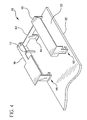
- FIG. 4 illustrates another embodiment of an antenna assembly 10 according to the present invention.
- the driven element 16 and the parasitic element 18 are coupled together via a coupling element 62 .
- the coupling element 62 includes a foot 64 for operatively coupling both the driven element 16 and the parasitic element 18 to the ground plane 20 of the communication device.
- the driven element 16 , parasitic element 18 , and coupling element 62 may be formed from as a single metal part and be fabricated, for example, using high-speed metal stamping processes. In this manner, a compact antenna assembly is provided which is suitable for incorporation within efficient, high volume production of communication devices.
- the antenna element may thus be utilized in conjunction with surface mount device (SMD) production techniques.
- SMD surface mount device
- FIG. 5 illustrates another embodiment of an antenna assembly according to the present invention.
- the antenna of FIG. 5 optimally operates over a pair of frequency ranges, for example, such as cell band (824-894 MHz.) and PCS band (1850-1990 MHz.) ranges. Operation over a higher frequency range is attained by addition of an extension element 66 to the driven conductor element 16 .
- extension element 66 is disposed at a left side edge of the third portion 36 of the driven element 16 .
- Dimensions of the extension element 66 which are sized to effectuate resonance at the higher frequency range, are provided in FIG. 8 and Table 1.
- FIG. 6 illustrates another embodiment of an antenna assembly according to the present invention.
- the driven element 16 , parasitic element 18 , and coupling element 62 are formed as a single unit and operatively connected to the ground plane member 20 at a single ground location via foot 64 .
- FIG. 7 illustrates yet another embodiment of an antenna assembly according to the present invention.
- the driven element 16 , parasitic element 18 , and coupling element 62 are disposed upon a dielectric block or substrate 72 .
- the driven element 16 , parasitic element 18 , and coupling element 62 may be a metal deposition upon the dielectric substrate 72 or formed using other known metal deposition or metal etching processes as those skilled in the relevant arts may appreciate.
- FIGS. 8 and 9, in conjunction with Table 1, disclose dimensions for preferred embodiments of an antenna assembly according to the present invention.
- FIG. 10 illustrates another embodiment of an antenna assembly according to the present invention, in particular a dual band antenna assembly suitable for operation over the cell band (824-894 MHz.) and PCS band (1850-1990 MHz.) frequency ranges.
- This antenna assembly includes low frequency and high frequency driven elements 16 , 17 and low frequency and high frequency parasitic elements 18 , 19 , and for example, all elements being formed as a single stamped metal part.
- a coupling element 62 operatively connects the driven elements 16 , 17 to the parasitic elements 18 , 19 and is formed as a portion of the stamped metal part.
- Coupling element 62 is, in turn, operatively connected to the ground plane member 20 of the communication device 8 at an upper edge thereof.
- Low frequency driven element 16 , low frequency parasitic element 18 , and high frequency parasitic element 19 are each defined by a substantially rectangular planar top surface 74 , 76 , 78 .
- the top surfaces 74 , 76 , 78 are substantially co-planar.
- the high frequency driven element 17 is defined by a substantially rectangular element 80 disposed at a side of the low frequency driven element 16 and downwardly angled toward a foot 82 . Foot 82 is disposed upon a dielectric element 84 to capacitively couple the high frequency driven element 17 to the ground plane member 20 of the communication device.
- Dielectric member 84 may be a ⁇ fraction (1/32) ⁇ inch thickness dielectric substrate having a dielectric constant between 1 and 10, and preferably about 3.0.
- Dielectric member 84 may be a dielectric substrate such as used for printed circuit boards, having a dielectric constant in the range of 1-10, or dielectric member 84 may be a chip capacitor.
- Low frequency driven element 16 and low frequency parasitic element 18 are each operatively coupled at one end to the ground plane member 20 of the communication device via a capacitive coupling 86 , 88 defined between a foot member 90 , 92 and the ground plane 20 .
- a dielectric element 94 may be disposed within each capacitive coupling 86 , 88 .
- high frequency parasitic element 19 includes a free end.
- the antenna assembly of FIG. 10 includes a feed point 12 at which a single conductor from the communication device may be coupled thereto. Operation at alternative frequency ranges may be practicable utilizing the concepts of this embodiment by scaling the relevant dimensions provided herein as those skilled in the arts will appreciate.
- FIG. 11 illustrates another embodiment a multiple band antenna assembly of the present invention.
- Driven element 16 is coupled at feed point 12 to the communication device via a single conductor.
- Driven element 16 is approximately ‘C’ shaped when view in profile and includes a top planar surface including the feed point 12 , a first leg element 26 operatively connected near the upper edge of the ground plane element 20 of the printed wiring board via foot member 40 , and a second leg element 28 capacitively coupled to the ground plane element 20 via foot 92 and capacitor element 94 .
- a parasitic element 18 is disposed relative the driven element 16 and is similarly shaped.
- Parasitic element 18 is directly or operatively connected at one end near the upper edge of the ground plane element 20 , and capacitively coupled at another end to the ground plane element 20 .
- a perpendicular coupling section 98 is disposed between the driven element 16 and the low frequency parasitic element 18 .
- Coupling section 98 is capactively coupled to the driven element 16 and the low frequency parasitic element 18 via capacitor elements 96 .
- the dielectric constant of the capacitor elements 96 may range from 1 (air) to approximately 10.
- Antenna assembly of FIG. 11 further includes a high frequency parasitic element 19 directly or operatively connected at one end to the ground plane element 20 of the telecommunication device.
- High frequency parasitic element 19 may be a conductive wire element having a nominal 0.05 inch thickness and including an upper portion substantially aligned with the conductive surface and conductive portion 24 , 50 , respectively, of the driven element 16 and low frequency parasitic element 18 .
- high frequency parasitic element 19 is angled relative to the low frequency parasitic element 18 by an angle “ ⁇ ” of between approximately 5-25 degrees.
- FIG. 12 illustrates yet another embodiment of an antenna assembly 10 according to the present invention.
- the low frequency driven element 16 is directly or operatively connected at a first end to an upper portion 102 of the printed wiring board 22 , and at a lower portion 104 of the printed wiring board 22 through capacitive coupler 86 , and at feed point 12 .
- Low frequency driven element 16 includes a top planar surface 106 including first and second portions 108 , 110 , the first portion 108 defined by a substantially rectangular area and the second portion 110 defined by a relatively smaller rectangular area.
- Feed point 12 is disposed within the second portion 110 of the top planar surface 106 .
- High frequency driven element 80 is directly coupled at an edge of the low frequency driven element 16 (at the second portion 110 ) and is capacitively coupled at the other end to the ground plane 20 of the printed wiring board via foot element 82 and dielectric element 84 .
- High frequency parasitic element 19 which is defined by a substantially rectangular area, is also capacitively coupled to the ground plane member 20 through common foot element 82 and dielectric element 84 .
- the low frequency parasitic element 18 which is disposed on the opposite side of the low frequency driven element 16 , is capacitively coupled at a first end to the ground plane element 20 of the printed wiring board and at the opposite end to a coupling element 62 directly connected to the ground plane element 20 .
- Low frequency parasitic element 18 includes a top planar surface 112 having a plurality of portions defined by varying width dimension. Coupling element 62 electrically connects the low frequency parasitic element 18 to the low frequency driven element 16 .
- FIG. 13 illustrates yet another embodiment of an antenna assembly 10 according to the present invention.
- the driven element 16 is directly or operatively connected at a first end to an upper portion 102 of the printed wiring board 22 , and at a lower portion 104 of the printed wiring board 22 through capacitive coupler 86 .
- the driven element 16 includes a top planar surface including first and second portions 108 , 110 , the first portion 108 defined by a substantially rectangular area and the second portion 110 defined by a relatively smaller rectangular area.
- Driven element 16 further includes a downwardly directed conductive surface 16 a which is coupled at a lower foot surface to a feed point 12 . Operation over a higher frequency range is attained by addition of an extension element 66 to the driven conductor element 16 .
- extension element 66 is disposed at a side edge away from the parasitic element 18 .
- Extension element 66 includes a downwardly directed conductive surface 66 a which is coupled at a lower foot surface to the feed point 12 .
- the feed point 12 is preferably disposed a predetermined distance above the surface of the printed wiring board 22 .
- the foot surface defining the feedpoint 12 is illustrated as a planar surface, though alternatively, the pair of downwardly directed surfaces 16 a , 66 a could be joined without the planar foot surface.
- the parasitic element 18 which is disposed on the side of the driven element 16 opposite the extension element 66 , is capacitively coupled at a first end to the ground plane element 20 of the printed wiring board 22 and at the opposite end to a coupling element 62 directly connected to the ground plane element 20 .
- Parasitic element 18 includes a top planar surface having a plurality of portions defined by varying width dimension. Coupling element 62 electrically connects the parasitic element 18 to the low frequency driven element 16 .
- a dual band antenna includes a driven element 16 for the lower frequency band and a high frequency driven element 17 disposed away therefrom.
- the high frequency and low frequency driven elements 16 , 17 are each defined by substantially planar rectangular portions which are coupled via a conductive spacer portion 114 .
- a feed point 12 is provided between the driven elements 16 , 17 and a signal conductor from the printed wiring board 22 .
- a low frequency parasitic element 18 is disposed further away from the low frequency driven element 16 as indicated.
- FIG. 15 illustrates another preferred embodiment of an antenna assembly according to the present invention wherein the driven elements 16 , 17 and the parasitic element 18 are disposed upon an upper major surface 118 of a dielectric block element 120 .
- the driven elements 16 , 17 and parasitic element 18 may be made as metal depositions upon the dielectric block or otherwise patterned from a plated dielectric stock material.
- Dielectric block element 120 has a dielectric constant of between 1 and 10, and more preferably approximately 3.0.
- the dielectric block 120 is supported a distance away from the printed wiring board 22 of the communication device by conductive spacer elements 124 .
- the spacer elements 124 additionally operatively or directly connect the driven elements 16 , 17 and parasitic elements 19 to the ground plane member 22 at attachment points 134 .
- Low frequency driven element 16 and the parasitic element 18 are each capacitively coupled at respective ends to the ground plane 20 .
- bottom plate elements 126 are disposed upon the opposite major surface 128 of the dielectric substrate 120 and are electrically coupled to the ground plane member 20 via truncated conductive spacer elements 124 .
- a tuner element 130 is disposed at one end of high frequency driven element 17 and may be adjusted relative to the ground plane element 20 to adjust the resonant frequency of the higher frequency antenna.
- FIG. 16 illustrates another aspect of the present invention which provides for an extended ground plane element 140 for use in conjunction with the antenna assemblies disclosed herein.
- the overall length of the ground plane member 20 , 140 (the electrical length) is preferably greater than one-quarter wavelength for a preselected wavelength in the operational frequency band. Applicants have determined that the electrical length of the ground plane 20 , 140 in large part determines the gain of the antenna assembly.
- One limitation of smaller hand held communication devices is that the ground plane 20 , 140 has an electrical length which is less than optimal.
- the ground plane length 20 , 140 may be extended by coupling a conductive panel 144 of the flip panel portion 142 to the main ground plane 20 of the printed wiring board 22 .
- the conductive panel 144 may be a separate conductor element or a conductive layer disposed upon an existing surface of the flip panel portion 142 .
- the coupling device 146 may be selected from among a group of known electrical coupling techniques as appreciated by those skilled in the relevant arts.
- the antenna assemblies provide improved directivity, broadband input impedance, increased signal strength, and increased battery life.
- the antenna of the present invention reduces radio frequency radiation incident to the user's body, and reduces the physical size requirements of directional antenna used in cell phone handsets, PCS devices and the like.
- the disclosed antenna also increases front-to-back ratios, reduces multipath interference, and is easily integrated into the rear panel portion of a cellular transceiver device to minimizes the risk of damage or interference. Additionally, beamwidth and bandwidth enhancement in the direction away from the user is achieved particularly when the antenna assembly is used in conjunction with hand-held wireless communication devices. Beamwidths of 1.5-2 times greater than for a dipole antenna have been recognized.
Landscapes
- Engineering & Computer Science (AREA)
- Computer Networks & Wireless Communication (AREA)
- Support Of Aerials (AREA)
- Details Of Aerials (AREA)
Abstract
Description
- This application claims the benefit of priority pursuant to 35 U.S.C. §119 of copending PCT application Ser. No. PCT/US00/30428 filed Nov. 4, 2000.
- PCT application Ser. No. PCT/US00/30428 filed Nov. 4, 2000, claimed the benefit of U.S. Provisional Application No. 60/163,515 filed Nov. 4, 1999.
- This application is a continuation-in-part application pursuant to 37 C.F.R. 1.53(b) of pending application Ser. No. 09/374,782, filed Sep. 16, 1999, which was a continuation-in-part of application Ser. No. 08/008,618 filed on Jan. 16, 1998, now U.S. Pat. No. 5,945,954.
- The present invention relates to an antenna assembly suitable for wireless transmission of analog and/or digital data, and more particularly to a parasitic element antenna assembly for single or multiple band wireless communications devices.
- There exists a need for an improved antenna assembly that provides a single and/or dual band response and which can be readily incorporated into a small wireless communications device (WCD). Size restrictions continue to be imposed on the radio components used in products such as portable telephones, personal digital assistants, pagers, etc. For wireless communications devices requiring a dual band response the problem is further complicated. Positioning the antenna assembly within the WCD remains critical to the overall appearance and performance of the device.
- Known antenna assemblies for wireless communication devices include:
- 1. External Single or Multi Band Wire Dipole
- Features of this antenna includes an external half wave antenna operating over one or more frequency range; a typical gain of +2 dBi; negligible front-to-back ratio; and minimal specific absorption rate (SAR) reduction (SAR 2.7 mw/g typ @ 0.5 watt transmit power level). Multiple band operation is possible with this antenna by including LC (inductor and capacitor) traps used to achieve multi band resonances.
- 2. External Single or Multi Band Asymmetric Wire Dipole
- Features of this antenna include an external quarter wave antenna operating over one or more frequency range; typical gain of +2 dBi; and minimal front-to-back ratio and SAR reduction. LC traps may also be used to achieve multi-band resonance.
- 3. Internal Single or Multi Band Asymmetric Dipole
- Features of this antenna include a quarter wave resonant conductor traces, which may be located on a planar printed circuit board; typical gain of +1-2 dBi; slight front-to-back ratio and reduced SAR (2.1 mw/g.). This antenna may include one or more feedpoints for multiple band operation. A second conductor may be necessary for additional band resonance.
- 4. Internal or Single Multi Band PIFA (Planar Inverted F Antenna)
- Features of this antenn include a single or multiple resonant planar conductor; typical gain of +1.5 dBi; and front-to-back ratio and SAR values being a function of frequency. A dual band PIFA antenna for 824-894/1850-1990 MHz operation may exhibit 2 dB gain and present minimal front-to-back ratio and reduced SAR of 2 mw/g in the lower frequency band.
- A compact single or multiple band antenna assembly for wireless communications devices is described. One multi-band implementation includes a high frequency portion and a low frequency portion, both fed at a common point by a single feedline. Both portions may be formed as a single stamped metal part or metallized plastic part. The overall size is suitable for integration within a wireless device such as a cellphone.
- Further, the low frequency portion consists of two resonant sections which are stagger tuned to achieve a wide resonant bandwidth, thus allowing greater tolerance for manufacturing variations and temperature than a single resonant section. This feature is useful for single band antennas as well as multi-band antennas. This feature may also be used to enhance bandwidth for both sections of a dual band antenna as well.
- The resonant sections for single or multi-band antennas operate in conjunction with a second planar conductor, which may be provided by the ground trace portion of the printed wiring board of a wireless communications device. An antenna assembly so formed provides a moderate front-to-back ratio of 3-12 dB and forward gain of +1 to +5 dBi. The front to back ratio reduces the near field toward the user of a hand held wireless communications device, thus reducing SAR (specific absorption rate) of RF energy by the body during transmit. Antenna pattern beamwidth and bandwidth is increased for a handset during normal user operation, as compared to a half wave dipole. An antenna assembly according to the present invention may provide increase beamwidth when the WCD is near the user head in the talk position, by a factor of 1.5-2.
- An object of the present invention is thus to satisfy the current trends which demand a reduction in size, weight, and cost for wireless communication devices.
- Another object of the present invention is the provision of multiple stagger-tuned resonant elements to enhance operational beamwidth and bandwidth, and providing an improved margin for manufacturing tolerances and environmental effects. An improved beamwidth and bandwidth of the handset may translate into improved communication by increasing the number of illuminated cell sites during operation.
- Another object of the present invention is the provision of an antenna assembly which is extremely compact in size relative to existing antenna assemblies. The antenna assembly may be incorporated internally within a wireless handset. A unique feed system without matching components is employed to couple the antenna to the RF port of the wireless handset. The antenna assembly requires three small-area RF ground lands for mounting, and is effectively a surface mount device (SMD). Beneficially, the antenna assembly may be handled and soldered like any other SMD electronic component. Because the antenna is small, the danger of damage is prevented as there are no external projections out of the WCD's housing. Additionally, portions of the antenna assembly may be disposed away from the printed wiring board and components thereof, allowing components to be disposed between the antenna assembly and the printed wiring board (PWB).
- Another object of the present invention is an antenna assembly providing substantially improved electrical performance versus volume ratio, and electrical performance versus cost as compared to known antenna assemblies. Gain of the antenna assembly according to the present invention may be nominally equal to an external ¼ wave wire antenna, with SAR level less than 1.6 mw/g achieved at 0.5 watt input for an internally mounted antenna. The 3 dB beamwidths are significantly higher than a dipole antenna during normal user operation. The performance characteristics are found across a wide range of environmental operating conditions, e.g, at temperatures ranging from −40 to +60 degrees C.
- Components of the antenna assembly may be manufactured in different ways. It is conceivable for example that the antenna can be formed from a punched or etched sheet. In a preferred embodiment, the antenna may be formed from a single-piece metal stamping adaptable to high volume production. Additionally, capacitor elements may be coupled to the antenna assembly through known high volume production techniques.
- Another object of the present invention is to provide an antenna assembly having improved operational characteristics, including an increased front-to-back ratio and a decreased specific absorption rate of RF energy to the user of an associated wireless communications device.
- Accordingly, it is the primary object of the present invention to provide an improved antenna assembly for communications devices including portable cellular telephones and PCS devices with improved directionality, broadband input impedance and increased signal strength. The present invention additionally reduces radio frequency radiation incident to the user's body and reduces the physical size requirements for a directional antenna assembly used on communications devices.
- It is still an additional object of the present invention to provide a compact antenna assembly suitable for incorporation within the housing of a portable wireless communication device. The current invention provides compact, discrete antenna assembly without external appendages, such as provided by known external dipole antennas.
- The accompanying drawings illustrate preferred embodiments of the invention and together with the description, serve to explain the principles of the invention. In the drawings:
- FIG. 1 is a perspective view of a communication device incorporating an antenna assembly according to the present invention;
- FIG. 2 is a perspective view of an antenna assembly according to the present invention;
- FIG. 3 is a perspective view of an antenna assembly according to the present invention;
- FIG. 4 is a perspective view of another embodiment of an antenna assembly according to the present invention;
- FIG. 5 is a perspective view of yet another embodiment of an antenna assembly according to the present invention including a dual band antenna circuit with parasitically coupled stagger tuned sections for the lower frequency band, and a single resonant section for the higher frequency band;
- FIG. 6 is a perspective view of yet another embodiment of an antenna assembly according to the present invention providing sections joined to facilitate construction as a single stamped part;
- FIG. 7 is a perspective view of yet another embodiment of an antenna assembly according to the present invention;
- FIG. 8 is a top plan view of an antenna assembly according to the present invention as represented in FIGS. 1-7;
- FIG. 9 is a side elevational view of the antenna assembly of FIG. 8;
- FIG. 10 is a perspective view of yet another embodiment of an antenna assembly according to the present invention;
- FIG. 11 is a perspective view of yet another embodiment of an antenna assembly according to the present invention;
- FIG. 12 is a perspective view of yet another embodiment of an antenna assembly according to the present invention;
- FIG. 13 is a perspective view of yet another embodiment of an antenna assembly according to the present invention;
- FIG. 14 is a perspective view of yet another embodiment of an antenna assembly according to the present invention;
- FIG. 15 is a perspective view of yet another embodiment of an antenna assembly according to the present invention; and
- FIG. 16 is a perspective view of a hand-held communications device according to another aspect of the present invention wherein the ground plane element of the antenna assembly is extended into a flip-portion of the communications device.
- Referring now to the drawings, wherein like numerals depict like parts throughout, FIG. 1 illustrates a
wireless communication device 8, such as a cellular telephone, utilizing anantenna assembly 10 according to the present invention and operating over the cell band frequency range of 824-894 MHz. Theantenna assembly 10 may be disposed within thecommunication device 8 at therear panel 14 and proximate the upper portion of the handset (away from a user's hand), as illustrated in the embodiment of FIG. 1. A first embodiment of anantenna assembly 10 includes a drivenconductor element 16 and aparasitic conductor element 18 each disposed relative to aground plane element 20 of thewireless communication device 8 is illustrated in FIGS. 2 and 3. Theground plane element 20 may be defined as a portion of the printed wiring board (PWB) 22 of thecommunication device 8. Drivenconductor element 16 includes aconductive surface 24 with first andsecond leg elements conductor element 16 may be a metallic chassis made, for example, of copper or a copper alloy. The drivenconductor element 16 is approximately “C” shaped when viewed from its side and defines aninterior region 30 disposed between theconductive surface 24 and theground plane element 20. Components of thecommunication device 8 may thus be disposed within theinterior region 30 to effect a reduction in overall volume of the device. - The
conductive surface 24 is disposed a predetermined distance above theground plane element 20 and includes a plurality of sections having different widths for effecting optimal operation over the cell band frequency range (824-894 MHz.). A firstrectangular section 32 is approximately 0.42 inch by 0.61 inch in size for a preferred embodiment. A secondrectangular section 34 disposed at an upper edge of thefirst section 32 is approximately 0.1 inch by 0.42 inch in size. A thirdrectangular section 36 disposed at an upper edge of thesecond section 34 is approximately 0.2 inch by 0.25 inch in size. A fourthrectangular section 38 disposed at an upper edge of thethird section 36 is approximately 0.15 inch by 0.13 inch in size. Other dimensions for a preferred embodiment of the present invention are disclosed in FIGS. 8-9 and Table 1. -
Conductive surface 24 is electrically or operatively connected at an upper edge of thefourth section 38 to a downwardly-directed, perpendicularfirst leg element 26 which is shorted to theground plane 20 atfoot 40. One ormore feet 40 may be practicable to provide for stability of the drivenelement 16 or routing requirements of the printedwiring board 22 of the communication device. Preferably asingle foot 40 is utilized to minimize the contact requirements to theground plane 20 and otherwise minimize physical interference with other components of the printedwiring board 22. -
Conductive surface 24 is also coupled at a lower edge of thefirst section 32 to a downwardly-directed perpendicular secondleg element surface 28.Second leg element 28 includes a ‘T’ shaped profile to minimize the interference with other components of the printedwiring board 22.Second leg element 28 includes aperpendicular foot 42 for capacitively coupling drivenconductor 16 to theground plane member 20. One ormore feet 42 may be practicable to provide for conductor stability or wire routing requirements of the printedcircuit board 22 the communication device.Ground plane element 20 preferably has a minimum length in a direction of polarization ‘DP’ of approximately one-quarter wavelength (for a wavelength within the range of operation). Reference may be made to FIG. 16, wherein an approach to extending theground plane member 20 of a small hand-held communication device is provided. Driven conductor element 16may be a single metallic formed element having a thickness within the range of 0.005 to 0.09 inch. -
Second leg element 28 includes afoot 42 which defines one side or plate of a twoplate capacitor 46.Foot 42 is spaced away from theground plane element 20 by adielectric element 48 so as to form a capacitor.Dielectric element 48 may have a dielectric constant of between 1-10, and preferably approximately 3.0. - The parasitic element 18of antenna assembly includes a ‘C’-shaped element which is spaced away from the driven
element 16.Parasitic element 18 includes aconductive portion 50 with first andsecond leg portions conductive leg portions second leg elements element 16.Parasitic element 18 is supported aboveground plane 20 by thesecond leg portion 54 which is capacitively coupled to theground plane 20 viafoot 56 anddielectric member 58. As with thefoot 42 and thedielectric element 48 of the drivenelement 16 forming a twoplate capacitor 46, thefoot 56 and thedielectric element 58 of theparasitic element 18 form a twoplate capacitor 60. Theparasitic element 18 is further supported by afirst leg portion 52 which is electrically or operatively connected to theground plane element 20 viafoot 40. Note that theparasitic element 18 includes aninterior region 68 similar to theinterior region 30 of the driven element. - FIG. 4 illustrates another embodiment of an
antenna assembly 10 according to the present invention. The drivenelement 16 and theparasitic element 18 are coupled together via acoupling element 62. Thecoupling element 62 includes afoot 64 for operatively coupling both the drivenelement 16 and theparasitic element 18 to theground plane 20 of the communication device. The drivenelement 16,parasitic element 18, andcoupling element 62 may be formed from as a single metal part and be fabricated, for example, using high-speed metal stamping processes. In this manner, a compact antenna assembly is provided which is suitable for incorporation within efficient, high volume production of communication devices. The antenna element may thus be utilized in conjunction with surface mount device (SMD) production techniques. - FIG. 5 illustrates another embodiment of an antenna assembly according to the present invention. The antenna of FIG. 5 optimally operates over a pair of frequency ranges, for example, such as cell band (824-894 MHz.) and PCS band (1850-1990 MHz.) ranges. Operation over a higher frequency range is attained by addition of an
extension element 66 to the drivenconductor element 16. Preferably,extension element 66 is disposed at a left side edge of thethird portion 36 of the drivenelement 16. Dimensions of theextension element 66, which are sized to effectuate resonance at the higher frequency range, are provided in FIG. 8 and Table 1. - FIG. 6 illustrates another embodiment of an antenna assembly according to the present invention. Similarly to FIG. 4, the driven
element 16,parasitic element 18, andcoupling element 62 are formed as a single unit and operatively connected to theground plane member 20 at a single ground location viafoot 64. - FIG. 7 illustrates yet another embodiment of an antenna assembly according to the present invention. The driven
element 16,parasitic element 18, andcoupling element 62 are disposed upon a dielectric block orsubstrate 72. The drivenelement 16,parasitic element 18, andcoupling element 62 may be a metal deposition upon thedielectric substrate 72 or formed using other known metal deposition or metal etching processes as those skilled in the relevant arts may appreciate. - FIGS. 8 and 9, in conjunction with Table 1, disclose dimensions for preferred embodiments of an antenna assembly according to the present invention.
- FIG. 10 illustrates another embodiment of an antenna assembly according to the present invention, in particular a dual band antenna assembly suitable for operation over the cell band (824-894 MHz.) and PCS band (1850-1990 MHz.) frequency ranges. This antenna assembly includes low frequency and high frequency driven
elements parasitic elements coupling element 62 operatively connects the drivenelements parasitic elements element 62 is, in turn, operatively connected to theground plane member 20 of thecommunication device 8 at an upper edge thereof. Low frequency drivenelement 16, low frequencyparasitic element 18, and high frequencyparasitic element 19 are each defined by a substantially rectangular planartop surface element 17 is defined by a substantiallyrectangular element 80 disposed at a side of the low frequency drivenelement 16 and downwardly angled toward afoot 82.Foot 82 is disposed upon adielectric element 84 to capacitively couple the high frequency drivenelement 17 to theground plane member 20 of the communication device.Dielectric member 84 may be a {fraction (1/32)} inch thickness dielectric substrate having a dielectric constant between 1 and 10, and preferably about 3.0.Dielectric member 84 may be a dielectric substrate such as used for printed circuit boards, having a dielectric constant in the range of 1-10, ordielectric member 84 may be a chip capacitor. - Low frequency driven
element 16 and low frequencyparasitic element 18 are each operatively coupled at one end to theground plane member 20 of the communication device via acapacitive coupling foot member ground plane 20. Adielectric element 94 may be disposed within eachcapacitive coupling parasitic element 19 includes a free end. - The antenna assembly of FIG. 10 includes a
feed point 12 at which a single conductor from the communication device may be coupled thereto. Operation at alternative frequency ranges may be practicable utilizing the concepts of this embodiment by scaling the relevant dimensions provided herein as those skilled in the arts will appreciate. - FIG. 11 illustrates another embodiment a multiple band antenna assembly of the present invention. Driven
element 16 is coupled atfeed point 12 to the communication device via a single conductor. Drivenelement 16 is approximately ‘C’ shaped when view in profile and includes a top planar surface including thefeed point 12, afirst leg element 26 operatively connected near the upper edge of theground plane element 20 of the printed wiring board viafoot member 40, and asecond leg element 28 capacitively coupled to theground plane element 20 viafoot 92 andcapacitor element 94. Aparasitic element 18 is disposed relative the drivenelement 16 and is similarly shaped.Parasitic element 18 is directly or operatively connected at one end near the upper edge of theground plane element 20, and capacitively coupled at another end to theground plane element 20. Aperpendicular coupling section 98 is disposed between the drivenelement 16 and the low frequencyparasitic element 18. Couplingsection 98 is capactively coupled to the drivenelement 16 and the low frequencyparasitic element 18 viacapacitor elements 96. The dielectric constant of thecapacitor elements 96 may range from 1 (air) to approximately 10. - Antenna assembly of FIG. 11 further includes a high frequency
parasitic element 19 directly or operatively connected at one end to theground plane element 20 of the telecommunication device. High frequencyparasitic element 19 may be a conductive wire element having a nominal 0.05 inch thickness and including an upper portion substantially aligned with the conductive surface andconductive portion element 16 and low frequencyparasitic element 18. Note that high frequencyparasitic element 19 is angled relative to the low frequencyparasitic element 18 by an angle “α” of between approximately 5-25 degrees. - FIG. 12 illustrates yet another embodiment of an
antenna assembly 10 according to the present invention. The low frequency drivenelement 16 is directly or operatively connected at a first end to anupper portion 102 of the printedwiring board 22, and at alower portion 104 of the printedwiring board 22 throughcapacitive coupler 86, and atfeed point 12. Low frequency drivenelement 16 includes a topplanar surface 106 including first andsecond portions first portion 108 defined by a substantially rectangular area and thesecond portion 110 defined by a relatively smaller rectangular area.Feed point 12 is disposed within thesecond portion 110 of the topplanar surface 106. High frequency drivenelement 80 is directly coupled at an edge of the low frequency driven element 16 (at the second portion 110) and is capacitively coupled at the other end to theground plane 20 of the printed wiring board viafoot element 82 anddielectric element 84. High frequencyparasitic element 19, which is defined by a substantially rectangular area, is also capacitively coupled to theground plane member 20 throughcommon foot element 82 anddielectric element 84. - Still referring to FIG. 12, the low frequency
parasitic element 18, which is disposed on the opposite side of the low frequency drivenelement 16, is capacitively coupled at a first end to theground plane element 20 of the printed wiring board and at the opposite end to acoupling element 62 directly connected to theground plane element 20. Low frequencyparasitic element 18 includes a topplanar surface 112 having a plurality of portions defined by varying width dimension. Couplingelement 62 electrically connects the low frequencyparasitic element 18 to the low frequency drivenelement 16. - FIG. 13 illustrates yet another embodiment of an
antenna assembly 10 according to the present invention. The drivenelement 16 is directly or operatively connected at a first end to anupper portion 102 of the printedwiring board 22, and at alower portion 104 of the printedwiring board 22 throughcapacitive coupler 86. The drivenelement 16 includes a top planar surface including first andsecond portions first portion 108 defined by a substantially rectangular area and thesecond portion 110 defined by a relatively smaller rectangular area. Drivenelement 16 further includes a downwardly directedconductive surface 16 a which is coupled at a lower foot surface to afeed point 12. Operation over a higher frequency range is attained by addition of anextension element 66 to the drivenconductor element 16. Preferably,extension element 66 is disposed at a side edge away from theparasitic element 18.Extension element 66 includes a downwardly directedconductive surface 66 a which is coupled at a lower foot surface to thefeed point 12. Thefeed point 12 is preferably disposed a predetermined distance above the surface of the printedwiring board 22. The foot surface defining thefeedpoint 12 is illustrated as a planar surface, though alternatively, the pair of downwardly directedsurfaces - Still referring to FIG. 13, the
parasitic element 18, which is disposed on the side of the drivenelement 16 opposite theextension element 66, is capacitively coupled at a first end to theground plane element 20 of the printedwiring board 22 and at the opposite end to acoupling element 62 directly connected to theground plane element 20.Parasitic element 18 includes a top planar surface having a plurality of portions defined by varying width dimension. Couplingelement 62 electrically connects theparasitic element 18 to the low frequency drivenelement 16. - Referring now to FIG. 14, another embodiment of an antenna assembly according to the present invention is provided. A dual band antenna includes a driven
element 16 for the lower frequency band and a high frequency drivenelement 17 disposed away therefrom. The high frequency and low frequency drivenelements conductive spacer portion 114. Afeed point 12 is provided between the drivenelements wiring board 22. A low frequencyparasitic element 18 is disposed further away from the low frequency drivenelement 16 as indicated. - FIG. 15 illustrates another preferred embodiment of an antenna assembly according to the present invention wherein the driven
elements parasitic element 18 are disposed upon an uppermajor surface 118 of adielectric block element 120. The drivenelements parasitic element 18 may be made as metal depositions upon the dielectric block or otherwise patterned from a plated dielectric stock material.Dielectric block element 120 has a dielectric constant of between 1 and 10, and more preferably approximately 3.0. Thedielectric block 120 is supported a distance away from the printedwiring board 22 of the communication device byconductive spacer elements 124. Thespacer elements 124 additionally operatively or directly connect the drivenelements parasitic elements 19 to theground plane member 22 at attachment points 134. Low frequency drivenelement 16 and theparasitic element 18 are each capacitively coupled at respective ends to theground plane 20. Note thatbottom plate elements 126 are disposed upon the oppositemajor surface 128 of thedielectric substrate 120 and are electrically coupled to theground plane member 20 via truncated conductivespacer elements 124. Atuner element 130 is disposed at one end of high frequency drivenelement 17 and may be adjusted relative to theground plane element 20 to adjust the resonant frequency of the higher frequency antenna. - FIG. 16 illustrates another aspect of the present invention which provides for an extended
ground plane element 140 for use in conjunction with the antenna assemblies disclosed herein. The overall length of theground plane member 20, 140 (the electrical length) is preferably greater than one-quarter wavelength for a preselected wavelength in the operational frequency band. Applicants have determined that the electrical length of theground plane ground plane flip panel portion 142, theground plane length conductive panel 144 of theflip panel portion 142 to themain ground plane 20 of the printedwiring board 22. Theconductive panel 144 may be a separate conductor element or a conductive layer disposed upon an existing surface of theflip panel portion 142. Thecoupling device 146 may be selected from among a group of known electrical coupling techniques as appreciated by those skilled in the relevant arts. - Particular dimensions for preferred embodiments according to the present invention are included as Table 1.
TABLE 1 Dimension Inch i. 1.600 j. 1.260 k. .925 l. .775 m. .725 n. .400 o. .200 p. .395 q. .200 r. 1.330 s. .100 t. .640 u. .420 v. .360 w. .610 x. .530 y. .950 z. 1.080 AA. 1.200 - In operation and use the antenna assemblies according to the present invention are extremely efficient and effective. The antenna assemblies provide improved directivity, broadband input impedance, increased signal strength, and increased battery life. The antenna of the present invention reduces radio frequency radiation incident to the user's body, and reduces the physical size requirements of directional antenna used in cell phone handsets, PCS devices and the like. The disclosed antenna also increases front-to-back ratios, reduces multipath interference, and is easily integrated into the rear panel portion of a cellular transceiver device to minimizes the risk of damage or interference. Additionally, beamwidth and bandwidth enhancement in the direction away from the user is achieved particularly when the antenna assembly is used in conjunction with hand-held wireless communication devices. Beamwidths of 1.5-2 times greater than for a dipole antenna have been recognized.
- Additional advantages and modification will readily occur to those skilled in the art. The invention in its broader aspects is, therefore, not limited to the specific details, representative apparatus and illustrative examples shown and described. Accordingly, departures from such details may be made without departing from the spirit or scope of the applicant's general inventive concept.
Claims (30)
Priority Applications (1)
| Application Number | Priority Date | Filing Date | Title |
|---|---|---|---|
| US09/828,532 US6429818B1 (en) | 1998-01-16 | 2001-04-06 | Single or dual band parasitic antenna assembly |
Applications Claiming Priority (6)
| Application Number | Priority Date | Filing Date | Title |
|---|---|---|---|
| US09/008,618 US5945954A (en) | 1998-01-16 | 1998-01-16 | Antenna assembly for telecommunication devices |
| US09/374,782 US6215447B1 (en) | 1998-01-16 | 1999-08-16 | Antenna assembly for communications devices |
| US16351599P | 1999-11-04 | 1999-11-04 | |
| PCT/US2000/030428 WO2001033665A1 (en) | 1999-11-04 | 2000-11-04 | Single or dual band parasitic antenna assembly |
| USPCT/US00/30428 | 2000-11-04 | ||
| US09/828,532 US6429818B1 (en) | 1998-01-16 | 2001-04-06 | Single or dual band parasitic antenna assembly |
Related Parent Applications (1)
| Application Number | Title | Priority Date | Filing Date |
|---|---|---|---|
| US09/374,782 Continuation-In-Part US6215447B1 (en) | 1998-01-16 | 1999-08-16 | Antenna assembly for communications devices |
Publications (2)
| Publication Number | Publication Date |
|---|---|
| US20020070902A1 true US20020070902A1 (en) | 2002-06-13 |
| US6429818B1 US6429818B1 (en) | 2002-08-06 |
Family
ID=27358655
Family Applications (1)
| Application Number | Title | Priority Date | Filing Date |
|---|---|---|---|
| US09/828,532 Expired - Fee Related US6429818B1 (en) | 1998-01-16 | 2001-04-06 | Single or dual band parasitic antenna assembly |
Country Status (1)
| Country | Link |
|---|---|
| US (1) | US6429818B1 (en) |
Cited By (27)
| Publication number | Priority date | Publication date | Assignee | Title |
|---|---|---|---|---|
| US20040046701A1 (en) * | 2001-03-07 | 2004-03-11 | Stefan Huber | Radio communications device comprising an sar value-reducing correction element |
| EP1414106A1 (en) * | 2002-10-22 | 2004-04-28 | Sony Ericsson Mobile Communications AB | Multiband radio antenna |
| WO2004038856A1 (en) * | 2002-10-22 | 2004-05-06 | Sony Ericsson Mobile Communications Ab | Multiband radio antenna |
| US20040145526A1 (en) * | 2001-04-16 | 2004-07-29 | Carles Puente Baliarda | Dual-band dual-polarized antenna array |
| US20050093750A1 (en) * | 2003-10-31 | 2005-05-05 | Vance Scott L. | Multi-band planar inverted-F antennas including floating parasitic elements and wireless terminals incorporating the same |
| EP1536242A1 (en) * | 2003-11-28 | 2005-06-01 | Maschek Elekronik | Dosimeter for electromagnetic fields |
| US20050116875A1 (en) * | 2003-11-28 | 2005-06-02 | Alps Electric Co., Ltd. | Antenna device suitable for miniaturization |
| US20050122268A1 (en) * | 2003-12-05 | 2005-06-09 | Alps Electric Co., Ltd. | Miniaturized antenna-coupled module |
| US20060033667A1 (en) * | 2002-02-13 | 2006-02-16 | Greg Johnson | Oriented PIFA-type device and method of use for reducing RF interference |
| US20060038721A1 (en) * | 2004-08-20 | 2006-02-23 | Mete Ozkar | Planar inverted "F" antenna and method of tuning same |
| US20060170600A1 (en) * | 2003-10-20 | 2006-08-03 | Lk Products Oy | Internal multiband antenna |
| US20060290575A1 (en) * | 2003-05-09 | 2006-12-28 | Heiko Pelzer | Antenna integrated into a housing |
| WO2007107101A1 (en) * | 2006-03-20 | 2007-09-27 | Matsushita Electric Industrial Co., Ltd. | Single feed internal antenna with multi-band for mobile communication terminals |
| US20080062045A1 (en) * | 2006-09-08 | 2008-03-13 | Motorola, Inc. | Communication device with a low profile antenna |
| US20080169984A1 (en) * | 2007-01-15 | 2008-07-17 | Naoyuki Takagi | Antenna |
| CN100420092C (en) * | 2002-06-21 | 2008-09-17 | 捷讯研究有限公司 | Multiple-element antenna with parasitic coupler |
| US7573424B2 (en) * | 2005-06-10 | 2009-08-11 | Hon Hai Precision Industry Co., Ltd. | Dual-band antenna for radiating electromagnetic signals of different frequencies |
| WO2010042853A1 (en) * | 2008-10-09 | 2010-04-15 | Johnson Greg F | Antenna system having compact pifa resonator with open section |
| US20110312393A1 (en) * | 2010-06-18 | 2011-12-22 | Motorola, Inc. | Antenna system with parasitic element for hearing aid compliant electromagnetic emission |
| US20120235871A1 (en) * | 2007-12-26 | 2012-09-20 | Murata Manufacturing Co., Ltd. | Antenna device and radio frequency ic device |
| US20130154895A1 (en) * | 2011-12-19 | 2013-06-20 | Microsoft Corporation | Integrated antenna structure |
| KR20160061178A (en) * | 2014-11-21 | 2016-05-31 | 삼성전자주식회사 | Antenna and electronic device having it |
| US20170077598A1 (en) * | 2015-09-11 | 2017-03-16 | Aclara Technologies Llc | Pit lid trident antenna arrangement |
| WO2018208363A1 (en) * | 2017-05-12 | 2018-11-15 | Commscope Technologies Llc | Base station antennas having parasitic coupling units |
| US11183775B2 (en) * | 2019-03-21 | 2021-11-23 | Commscope Technologies Llc | Base station antennas having parasitic assemblies for improving cross-polarization discrimination performance |
| US20210376478A1 (en) * | 2020-05-28 | 2021-12-02 | Avx Antenna, Inc. D/B/A Ethertronics, Inc. | Modal Antenna System Including Closed-Loop Parasitic Element |
| US11962102B2 (en) | 2021-06-17 | 2024-04-16 | Neptune Technology Group Inc. | Multi-band stamped sheet metal antenna |
Families Citing this family (66)
| Publication number | Priority date | Publication date | Assignee | Title |
|---|---|---|---|---|
| DE69924535T2 (en) | 1999-09-20 | 2006-02-16 | Fractus, S.A. | MULTILEVEL ANTENNA |
| EP1329985A3 (en) * | 2002-01-18 | 2004-12-22 | Matsushita Electric Industrial Co., Ltd. | Antenna apparatus; communication apparatus; and antenna apparatus designing method |
| WO2004030143A1 (en) * | 2002-09-27 | 2004-04-08 | Radiall Antenna Technologies, Inc. | Compact vehicle-mounted antenna |
| TW547785U (en) * | 2002-11-13 | 2003-08-11 | Hon Hai Prec Ind Co Ltd | Wide-band antenna |
| US20040110481A1 (en) * | 2002-12-07 | 2004-06-10 | Umesh Navsariwala | Antenna and wireless device utilizing the antenna |
| FI116332B (en) * | 2002-12-16 | 2005-10-31 | Lk Products Oy | Antenna for a flat radio |
| WO2005006494A1 (en) * | 2003-06-11 | 2005-01-20 | Bae Systems Information And Electronic Systems Integration Inc. | Method and appartus for limiting vswr spikes in a compact broadband meander line loaded antenna assembly |
| KR100625121B1 (en) * | 2003-07-01 | 2006-09-19 | 에스케이 텔레콤주식회사 | Method and Apparatus for Reducing SAR Exposure in a Communication Handset Device |
| JP4152840B2 (en) * | 2003-09-11 | 2008-09-17 | 太陽誘電株式会社 | Communication device |
| US7034769B2 (en) * | 2003-11-24 | 2006-04-25 | Sandbridge Technologies, Inc. | Modified printed dipole antennas for wireless multi-band communication systems |
| US7095382B2 (en) * | 2003-11-24 | 2006-08-22 | Sandbridge Technologies, Inc. | Modified printed dipole antennas for wireless multi-band communications systems |
| US20060001576A1 (en) * | 2004-06-30 | 2006-01-05 | Ethertronics, Inc. | Compact, multi-element volume reuse antenna |
| FI20055420A0 (en) | 2005-07-25 | 2005-07-25 | Lk Products Oy | Adjustable multi-band antenna |
| FI119009B (en) | 2005-10-03 | 2008-06-13 | Pulse Finland Oy | Multiple-band antenna |
| FI118782B (en) | 2005-10-14 | 2008-03-14 | Pulse Finland Oy | Adjustable antenna |
| TWM307204U (en) * | 2006-05-02 | 2007-03-01 | Hon Hai Prec Ind Co Ltd | Multi-band antenna assembly |
| US8618990B2 (en) | 2011-04-13 | 2013-12-31 | Pulse Finland Oy | Wideband antenna and methods |
| FI20075269A0 (en) | 2007-04-19 | 2007-04-19 | Pulse Finland Oy | Method and arrangement for antenna matching |
| US9035836B2 (en) * | 2007-08-20 | 2015-05-19 | Ethertronics, Inc. | Superimposed multimode antenna for enhanced system filtering |
| FI120427B (en) | 2007-08-30 | 2009-10-15 | Pulse Finland Oy | Adjustable multiband antenna |
| TWI369028B (en) * | 2007-09-10 | 2012-07-21 | Hon Hai Prec Ind Co Ltd | Multi-band antenna |
| US9917359B2 (en) | 2008-03-05 | 2018-03-13 | Ethertronics, Inc. | Repeater with multimode antenna |
| US9748637B2 (en) | 2008-03-05 | 2017-08-29 | Ethertronics, Inc. | Antenna and method for steering antenna beam direction for wifi applications |
| US8988289B2 (en) * | 2008-03-05 | 2015-03-24 | Ethertronics, Inc. | Antenna system for interference supression |
| US9761940B2 (en) | 2008-03-05 | 2017-09-12 | Ethertronics, Inc. | Modal adaptive antenna using reference signal LTE protocol |
| US20130109333A1 (en) * | 2011-07-25 | 2013-05-02 | Sebastian Rowson | Method and system for switched combined diversity with a modal antenna |
| US8339322B2 (en) | 2009-02-19 | 2012-12-25 | Galtronics Corporation Ltd. | Compact multi-band antennas |
| FI20096134A0 (en) | 2009-11-03 | 2009-11-03 | Pulse Finland Oy | Adjustable antenna |
| FI20096251A0 (en) | 2009-11-27 | 2009-11-27 | Pulse Finland Oy | MIMO antenna |
| US8847833B2 (en) | 2009-12-29 | 2014-09-30 | Pulse Finland Oy | Loop resonator apparatus and methods for enhanced field control |
| FI20105158A (en) | 2010-02-18 | 2011-08-19 | Pulse Finland Oy | SHELL RADIATOR ANTENNA |
| US9406998B2 (en) | 2010-04-21 | 2016-08-02 | Pulse Finland Oy | Distributed multiband antenna and methods |
| FI20115072A0 (en) | 2011-01-25 | 2011-01-25 | Pulse Finland Oy | Multi-resonance antenna, antenna module and radio unit |
| US9673507B2 (en) | 2011-02-11 | 2017-06-06 | Pulse Finland Oy | Chassis-excited antenna apparatus and methods |
| US8648752B2 (en) | 2011-02-11 | 2014-02-11 | Pulse Finland Oy | Chassis-excited antenna apparatus and methods |
| US8638265B2 (en) | 2011-03-11 | 2014-01-28 | Microsoft Corporation | Slot antenna |
| US8866689B2 (en) | 2011-07-07 | 2014-10-21 | Pulse Finland Oy | Multi-band antenna and methods for long term evolution wireless system |
| US9450291B2 (en) | 2011-07-25 | 2016-09-20 | Pulse Finland Oy | Multiband slot loop antenna apparatus and methods |
| US8963794B2 (en) | 2011-08-23 | 2015-02-24 | Apple Inc. | Distributed loop antennas |
| US8854266B2 (en) | 2011-08-23 | 2014-10-07 | Apple Inc. | Antenna isolation elements |
| US9123990B2 (en) | 2011-10-07 | 2015-09-01 | Pulse Finland Oy | Multi-feed antenna apparatus and methods |
| CN202276339U (en) * | 2011-10-18 | 2012-06-13 | 中兴通讯股份有限公司 | Wireless terminal |
| US9178278B2 (en) | 2011-11-17 | 2015-11-03 | Apple Inc. | Distributed loop antennas with extended tails |
| US9531058B2 (en) | 2011-12-20 | 2016-12-27 | Pulse Finland Oy | Loosely-coupled radio antenna apparatus and methods |
| US9484619B2 (en) | 2011-12-21 | 2016-11-01 | Pulse Finland Oy | Switchable diversity antenna apparatus and methods |
| US8988296B2 (en) | 2012-04-04 | 2015-03-24 | Pulse Finland Oy | Compact polarized antenna and methods |
| US9203139B2 (en) | 2012-05-04 | 2015-12-01 | Apple Inc. | Antenna structures having slot-based parasitic elements |
| US9979078B2 (en) | 2012-10-25 | 2018-05-22 | Pulse Finland Oy | Modular cell antenna apparatus and methods |
| US10069209B2 (en) | 2012-11-06 | 2018-09-04 | Pulse Finland Oy | Capacitively coupled antenna apparatus and methods |
| US10079428B2 (en) | 2013-03-11 | 2018-09-18 | Pulse Finland Oy | Coupled antenna structure and methods |
| US9647338B2 (en) | 2013-03-11 | 2017-05-09 | Pulse Finland Oy | Coupled antenna structure and methods |
| US9634383B2 (en) | 2013-06-26 | 2017-04-25 | Pulse Finland Oy | Galvanically separated non-interacting antenna sector apparatus and methods |
| US9680212B2 (en) | 2013-11-20 | 2017-06-13 | Pulse Finland Oy | Capacitive grounding methods and apparatus for mobile devices |
| CN104681979B (en) * | 2013-11-30 | 2019-04-12 | 深圳富泰宏精密工业有限公司 | Wide frequency antenna structure and wireless communication device with the wide frequency antenna structure |
| US9590308B2 (en) | 2013-12-03 | 2017-03-07 | Pulse Electronics, Inc. | Reduced surface area antenna apparatus and mobile communications devices incorporating the same |
| US10069479B1 (en) | 2013-12-31 | 2018-09-04 | Ethertronics, Inc. | Tunable filter for RF circuits |
| US9350081B2 (en) | 2014-01-14 | 2016-05-24 | Pulse Finland Oy | Switchable multi-radiator high band antenna apparatus |
| TWI538307B (en) * | 2014-06-16 | 2016-06-11 | 智易科技股份有限公司 | Dual-band three-dimensional antenna |
| US9973228B2 (en) | 2014-08-26 | 2018-05-15 | Pulse Finland Oy | Antenna apparatus with an integrated proximity sensor and methods |
| US9948002B2 (en) | 2014-08-26 | 2018-04-17 | Pulse Finland Oy | Antenna apparatus with an integrated proximity sensor and methods |
| US9722308B2 (en) | 2014-08-28 | 2017-08-01 | Pulse Finland Oy | Low passive intermodulation distributed antenna system for multiple-input multiple-output systems and methods of use |
| CN204375915U (en) * | 2014-11-10 | 2015-06-03 | 瑞声科技(南京)有限公司 | Multiband antenna |
| US9906260B2 (en) | 2015-07-30 | 2018-02-27 | Pulse Finland Oy | Sensor-based closed loop antenna swapping apparatus and methods |
| US10498030B2 (en) * | 2016-06-27 | 2019-12-03 | Intel IP Corporation | Frequency reconfigurable antenna decoupling for wireless communication |
| USD824885S1 (en) * | 2017-02-25 | 2018-08-07 | Airgain Incorporated | Multiple antennas assembly |
| GB2571279B (en) | 2018-02-21 | 2022-03-09 | Pet Tech Limited | Antenna arrangement and associated method |
Family Cites Families (8)
| Publication number | Priority date | Publication date | Assignee | Title |
|---|---|---|---|---|
| AT393054B (en) | 1989-07-27 | 1991-08-12 | Siemens Ag Oesterreich | TRANSMITTER AND / OR RECEIVING ARRANGEMENT FOR PORTABLE DEVICES |
| US5598169A (en) * | 1995-03-24 | 1997-01-28 | Lucent Technologies Inc. | Detector and modulator circuits for passive microwave links |
| US5644319A (en) * | 1995-05-31 | 1997-07-01 | Industrial Technology Research Institute | Multi-resonance horizontal-U shaped antenna |
| US5627550A (en) * | 1995-06-15 | 1997-05-06 | Nokia Mobile Phones Ltd. | Wideband double C-patch antenna including gap-coupled parasitic elements |
| EP0795926B1 (en) | 1996-03-13 | 2002-12-11 | Ascom Systec AG | Flat, three-dimensional antenna |
| US5764190A (en) * | 1996-07-15 | 1998-06-09 | The Hong Kong University Of Science & Technology | Capacitively loaded PIFA |
| US5880697A (en) | 1996-09-25 | 1999-03-09 | Torrey Science Corporation | Low-profile multi-band antenna |
| US6114996A (en) * | 1997-03-31 | 2000-09-05 | Qualcomm Incorporated | Increased bandwidth patch antenna |
-
2001
- 2001-04-06 US US09/828,532 patent/US6429818B1/en not_active Expired - Fee Related
Cited By (47)
| Publication number | Priority date | Publication date | Assignee | Title |
|---|---|---|---|---|
| US20040046701A1 (en) * | 2001-03-07 | 2004-03-11 | Stefan Huber | Radio communications device comprising an sar value-reducing correction element |
| US6937206B2 (en) * | 2001-04-16 | 2005-08-30 | Fractus, S.A. | Dual-band dual-polarized antenna array |
| US20040145526A1 (en) * | 2001-04-16 | 2004-07-29 | Carles Puente Baliarda | Dual-band dual-polarized antenna array |
| US7230574B2 (en) * | 2002-02-13 | 2007-06-12 | Greg Johnson | Oriented PIFA-type device and method of use for reducing RF interference |
| US20060033667A1 (en) * | 2002-02-13 | 2006-02-16 | Greg Johnson | Oriented PIFA-type device and method of use for reducing RF interference |
| CN100420092C (en) * | 2002-06-21 | 2008-09-17 | 捷讯研究有限公司 | Multiple-element antenna with parasitic coupler |
| US20060099914A1 (en) * | 2002-10-22 | 2006-05-11 | Johan Andersson | Multiband radio antenna |
| US7415248B2 (en) | 2002-10-22 | 2008-08-19 | Sony Ericsson Mobile Communications Ab | Multiband radio antenna with a flat parasitic element |
| WO2004038856A1 (en) * | 2002-10-22 | 2004-05-06 | Sony Ericsson Mobile Communications Ab | Multiband radio antenna |
| EP1414106A1 (en) * | 2002-10-22 | 2004-04-28 | Sony Ericsson Mobile Communications AB | Multiband radio antenna |
| US20060290575A1 (en) * | 2003-05-09 | 2006-12-28 | Heiko Pelzer | Antenna integrated into a housing |
| US20060170600A1 (en) * | 2003-10-20 | 2006-08-03 | Lk Products Oy | Internal multiband antenna |
| US7256743B2 (en) | 2003-10-20 | 2007-08-14 | Pulse Finland Oy | Internal multiband antenna |
| US6943733B2 (en) * | 2003-10-31 | 2005-09-13 | Sony Ericsson Mobile Communications, Ab | Multi-band planar inverted-F antennas including floating parasitic elements and wireless terminals incorporating the same |
| US20050093750A1 (en) * | 2003-10-31 | 2005-05-05 | Vance Scott L. | Multi-band planar inverted-F antennas including floating parasitic elements and wireless terminals incorporating the same |
| US20050116875A1 (en) * | 2003-11-28 | 2005-06-02 | Alps Electric Co., Ltd. | Antenna device suitable for miniaturization |
| EP1536242A1 (en) * | 2003-11-28 | 2005-06-01 | Maschek Elekronik | Dosimeter for electromagnetic fields |
| US20050122268A1 (en) * | 2003-12-05 | 2005-06-09 | Alps Electric Co., Ltd. | Miniaturized antenna-coupled module |
| US7123197B2 (en) * | 2003-12-05 | 2006-10-17 | Alps Electric Co., Ltd. | Miniaturized antenna-coupled module |
| US20060038721A1 (en) * | 2004-08-20 | 2006-02-23 | Mete Ozkar | Planar inverted "F" antenna and method of tuning same |
| US7345634B2 (en) * | 2004-08-20 | 2008-03-18 | Kyocera Corporation | Planar inverted “F” antenna and method of tuning same |
| US7573424B2 (en) * | 2005-06-10 | 2009-08-11 | Hon Hai Precision Industry Co., Ltd. | Dual-band antenna for radiating electromagnetic signals of different frequencies |
| WO2007107101A1 (en) * | 2006-03-20 | 2007-09-27 | Matsushita Electric Industrial Co., Ltd. | Single feed internal antenna with multi-band for mobile communication terminals |
| US20080062045A1 (en) * | 2006-09-08 | 2008-03-13 | Motorola, Inc. | Communication device with a low profile antenna |
| US20080169984A1 (en) * | 2007-01-15 | 2008-07-17 | Naoyuki Takagi | Antenna |
| US7528783B2 (en) * | 2007-01-15 | 2009-05-05 | Panasonic Corporation | Antenna |
| US8915448B2 (en) * | 2007-12-26 | 2014-12-23 | Murata Manufacturing Co., Ltd. | Antenna device and radio frequency IC device |
| US20120235871A1 (en) * | 2007-12-26 | 2012-09-20 | Murata Manufacturing Co., Ltd. | Antenna device and radio frequency ic device |
| WO2010042853A1 (en) * | 2008-10-09 | 2010-04-15 | Johnson Greg F | Antenna system having compact pifa resonator with open section |
| US20100271279A1 (en) * | 2008-10-09 | 2010-10-28 | Johnson Greg F | Antenna System Having Compact PIFA Resonator with Open Sections |
| US8354964B2 (en) | 2008-10-09 | 2013-01-15 | Johnson Greg F | Antenna system having compact PIFA resonator with open sections |
| US8483415B2 (en) * | 2010-06-18 | 2013-07-09 | Motorola Mobility Llc | Antenna system with parasitic element for hearing aid compliant electromagnetic emission |
| US20130273963A1 (en) * | 2010-06-18 | 2013-10-17 | Motorola Mobiltiy LLC | Antenna system with parasitic element for hearing aid compliant electromagnetic emission |
| US8605922B2 (en) * | 2010-06-18 | 2013-12-10 | Motorola Mobility Llc | Antenna system with parasitic element for hearing aid compliant electromagnetic emission |
| US20110312393A1 (en) * | 2010-06-18 | 2011-12-22 | Motorola, Inc. | Antenna system with parasitic element for hearing aid compliant electromagnetic emission |
| US20130154895A1 (en) * | 2011-12-19 | 2013-06-20 | Microsoft Corporation | Integrated antenna structure |
| KR102207852B1 (en) * | 2014-11-21 | 2021-01-26 | 삼성전자주식회사 | Antenna and electronic device having it |
| KR20160061178A (en) * | 2014-11-21 | 2016-05-31 | 삼성전자주식회사 | Antenna and electronic device having it |
| US20170077598A1 (en) * | 2015-09-11 | 2017-03-16 | Aclara Technologies Llc | Pit lid trident antenna arrangement |
| US10243264B2 (en) * | 2015-09-11 | 2019-03-26 | Aclara Technologies Llc | Pit lid trident antenna arrangement |
| WO2018208363A1 (en) * | 2017-05-12 | 2018-11-15 | Commscope Technologies Llc | Base station antennas having parasitic coupling units |
| US10431877B2 (en) | 2017-05-12 | 2019-10-01 | Commscope Technologies Llc | Base station antennas having parasitic coupling units |
| US11108135B2 (en) | 2017-05-12 | 2021-08-31 | Commscope Technologies Llc | Base station antennas having parasitic coupling units |
| US11183775B2 (en) * | 2019-03-21 | 2021-11-23 | Commscope Technologies Llc | Base station antennas having parasitic assemblies for improving cross-polarization discrimination performance |
| US20210376478A1 (en) * | 2020-05-28 | 2021-12-02 | Avx Antenna, Inc. D/B/A Ethertronics, Inc. | Modal Antenna System Including Closed-Loop Parasitic Element |
| US11735826B2 (en) * | 2020-05-28 | 2023-08-22 | KYOCERA AVX Components (San Diego), Inc. | Modal antenna system including closed-loop parasitic element |
| US11962102B2 (en) | 2021-06-17 | 2024-04-16 | Neptune Technology Group Inc. | Multi-band stamped sheet metal antenna |
Also Published As
| Publication number | Publication date |
|---|---|
| US6429818B1 (en) | 2002-08-06 |
Similar Documents
| Publication | Publication Date | Title |
|---|---|---|
| US6429818B1 (en) | Single or dual band parasitic antenna assembly | |
| US6456249B1 (en) | Single or dual band parasitic antenna assembly | |
| WO2001033665A1 (en) | Single or dual band parasitic antenna assembly | |
| US6215447B1 (en) | Antenna assembly for communications devices | |
| US6404394B1 (en) | Dual polarization slot antenna assembly | |
| US6407710B2 (en) | Compact dual frequency antenna with multiple polarization | |
| US6268831B1 (en) | Inverted-f antennas with multiple planar radiating elements and wireless communicators incorporating same | |
| US6326927B1 (en) | Capacitively-tuned broadband antenna structure | |
| US7319431B2 (en) | Surface mount antenna apparatus having triple land structure | |
| US7564413B2 (en) | Multi-band antenna and mobile communication terminal having the same | |
| US20060033667A1 (en) | Oriented PIFA-type device and method of use for reducing RF interference | |
| US20020075187A1 (en) | Low SAR broadband antenna assembly | |
| US20100060528A1 (en) | Dual-frequency antenna | |
| WO2003069729A1 (en) | Oriented pifa-type device and method of use for reducing rf interference | |
| US7050009B2 (en) | Internal antenna | |
| US6563466B2 (en) | Multi-frequency band inverted-F antennas with coupled branches and wireless communicators incorporating same | |
| US20020177416A1 (en) | Radio communications device | |
| US6646619B2 (en) | Broadband antenna assembly of matching circuitry and ground plane conductive radiating element | |
| US6515627B2 (en) | Multiple band antenna having isolated feeds | |
| US6697023B1 (en) | Built-in multi-band mobile phone antenna with meandering conductive portions | |
| EP1717901B1 (en) | Built-in type antenna apparatus for portable terminal | |
| KR20020065811A (en) | Printed slot microstrip antenna with EM coupling feed system | |
| US6683574B2 (en) | Twin monopole antenna | |
| KR20040051002A (en) | Printed Multiband Antenna | |
| KR20020039920A (en) | Stacked S-type multi-band internal antenna for mobile phone |
Legal Events
| Date | Code | Title | Description |
|---|---|---|---|
| AS | Assignment |
Owner name: RANGESTAR WIRELESS, INC., CALIFORNIA Free format text: ASSIGNMENT OF ASSIGNORS INTEREST;ASSIGNOR:JOHNSON, GREG;REEL/FRAME:011691/0275 Effective date: 20010405 |
|
| AS | Assignment |
Owner name: TYCO ELECTRONICS LOGISTICS AG, SWITZERLAND Free format text: ASSIGNMENT OF ASSIGNORS INTEREST;ASSIGNOR:RANGESTAR WIRELESS, INC.;REEL/FRAME:012683/0307 Effective date: 20010928 |
|
| FPAY | Fee payment |
Year of fee payment: 4 |
|
| FPAY | Fee payment |
Year of fee payment: 8 |
|
| REMI | Maintenance fee reminder mailed | ||
| LAPS | Lapse for failure to pay maintenance fees | ||
| STCH | Information on status: patent discontinuation |
Free format text: PATENT EXPIRED DUE TO NONPAYMENT OF MAINTENANCE FEES UNDER 37 CFR 1.362 |
|
| FP | Lapsed due to failure to pay maintenance fee |
Effective date: 20140806 |