US11476166B2 - Nano-sheet-based complementary metal-oxide-semiconductor devices with asymmetric inner spacers - Google Patents
Nano-sheet-based complementary metal-oxide-semiconductor devices with asymmetric inner spacers Download PDFInfo
- Publication number
- US11476166B2 US11476166B2 US16/875,726 US202016875726A US11476166B2 US 11476166 B2 US11476166 B2 US 11476166B2 US 202016875726 A US202016875726 A US 202016875726A US 11476166 B2 US11476166 B2 US 11476166B2
- Authority
- US
- United States
- Prior art keywords
- source
- semiconductor layers
- pair
- stack
- drain
- Prior art date
- Legal status (The legal status is an assumption and is not a legal conclusion. Google has not performed a legal analysis and makes no representation as to the accuracy of the status listed.)
- Active
Links
- 239000004065 semiconductor Substances 0.000 title claims abstract description 258
- 125000006850 spacer group Chemical group 0.000 title claims description 151
- 239000002135 nanosheet Substances 0.000 title description 44
- 230000000295 complement effect Effects 0.000 title description 3
- 239000000758 substrate Substances 0.000 claims abstract description 41
- 239000000463 material Substances 0.000 claims description 47
- 229910052751 metal Inorganic materials 0.000 claims description 23
- 239000002184 metal Substances 0.000 claims description 23
- 239000002019 doping agent Substances 0.000 claims description 15
- 239000010410 layer Substances 0.000 description 305
- 238000000034 method Methods 0.000 description 194
- 230000008569 process Effects 0.000 description 136
- 238000005530 etching Methods 0.000 description 52
- 239000003989 dielectric material Substances 0.000 description 35
- 238000000926 separation method Methods 0.000 description 25
- 238000012545 processing Methods 0.000 description 19
- 238000002955 isolation Methods 0.000 description 13
- 229910000577 Silicon-germanium Inorganic materials 0.000 description 12
- 238000004519 manufacturing process Methods 0.000 description 12
- 238000001039 wet etching Methods 0.000 description 10
- 238000000231 atomic layer deposition Methods 0.000 description 9
- VYPSYNLAJGMNEJ-UHFFFAOYSA-N Silicium dioxide Chemical compound O=[Si]=O VYPSYNLAJGMNEJ-UHFFFAOYSA-N 0.000 description 8
- XUIMIQQOPSSXEZ-UHFFFAOYSA-N Silicon Chemical compound [Si] XUIMIQQOPSSXEZ-UHFFFAOYSA-N 0.000 description 8
- 239000003990 capacitor Substances 0.000 description 8
- 238000005229 chemical vapour deposition Methods 0.000 description 8
- 229910052710 silicon Inorganic materials 0.000 description 8
- 239000010703 silicon Substances 0.000 description 8
- 229910052814 silicon oxide Inorganic materials 0.000 description 8
- 230000008901 benefit Effects 0.000 description 7
- 230000015572 biosynthetic process Effects 0.000 description 7
- 230000006870 function Effects 0.000 description 7
- 230000012010 growth Effects 0.000 description 7
- 239000000203 mixture Substances 0.000 description 7
- 238000000059 patterning Methods 0.000 description 6
- 229910052581 Si3N4 Inorganic materials 0.000 description 5
- 229910052796 boron Inorganic materials 0.000 description 5
- 238000000151 deposition Methods 0.000 description 5
- 230000000873 masking effect Effects 0.000 description 5
- 230000003647 oxidation Effects 0.000 description 5
- 238000007254 oxidation reaction Methods 0.000 description 5
- 238000005240 physical vapour deposition Methods 0.000 description 5
- 230000002829 reductive effect Effects 0.000 description 5
- 239000000126 substance Substances 0.000 description 5
- OKTJSMMVPCPJKN-UHFFFAOYSA-N Carbon Chemical compound [C] OKTJSMMVPCPJKN-UHFFFAOYSA-N 0.000 description 4
- PXHVJJICTQNCMI-UHFFFAOYSA-N Nickel Chemical compound [Ni] PXHVJJICTQNCMI-UHFFFAOYSA-N 0.000 description 4
- 229910052799 carbon Inorganic materials 0.000 description 4
- 238000000708 deep reactive-ion etching Methods 0.000 description 4
- 238000001312 dry etching Methods 0.000 description 4
- 238000005516 engineering process Methods 0.000 description 4
- 239000012212 insulator Substances 0.000 description 4
- 238000001459 lithography Methods 0.000 description 4
- 238000000206 photolithography Methods 0.000 description 4
- BASFCYQUMIYNBI-UHFFFAOYSA-N platinum Chemical compound [Pt] BASFCYQUMIYNBI-UHFFFAOYSA-N 0.000 description 4
- HQVNEWCFYHHQES-UHFFFAOYSA-N silicon nitride Chemical compound N12[Si]34N5[Si]62N3[Si]51N64 HQVNEWCFYHHQES-UHFFFAOYSA-N 0.000 description 4
- ZOXJGFHDIHLPTG-UHFFFAOYSA-N Boron Chemical compound [B] ZOXJGFHDIHLPTG-UHFFFAOYSA-N 0.000 description 3
- 229910052782 aluminium Inorganic materials 0.000 description 3
- 238000003486 chemical etching Methods 0.000 description 3
- 239000010949 copper Substances 0.000 description 3
- 238000013461 design Methods 0.000 description 3
- 239000002070 nanowire Substances 0.000 description 3
- 238000000623 plasma-assisted chemical vapour deposition Methods 0.000 description 3
- 229910052707 ruthenium Inorganic materials 0.000 description 3
- 229910003468 tantalcarbide Inorganic materials 0.000 description 3
- VHUUQVKOLVNVRT-UHFFFAOYSA-N Ammonium hydroxide Chemical compound [NH4+].[OH-] VHUUQVKOLVNVRT-UHFFFAOYSA-N 0.000 description 2
- JBRZTFJDHDCESZ-UHFFFAOYSA-N AsGa Chemical compound [As]#[Ga] JBRZTFJDHDCESZ-UHFFFAOYSA-N 0.000 description 2
- IJGRMHOSHXDMSA-UHFFFAOYSA-N Atomic nitrogen Chemical compound N#N IJGRMHOSHXDMSA-UHFFFAOYSA-N 0.000 description 2
- OAICVXFJPJFONN-UHFFFAOYSA-N Phosphorus Chemical compound [P] OAICVXFJPJFONN-UHFFFAOYSA-N 0.000 description 2
- KJTLSVCANCCWHF-UHFFFAOYSA-N Ruthenium Chemical compound [Ru] KJTLSVCANCCWHF-UHFFFAOYSA-N 0.000 description 2
- GWEVSGVZZGPLCZ-UHFFFAOYSA-N Titan oxide Chemical compound O=[Ti]=O GWEVSGVZZGPLCZ-UHFFFAOYSA-N 0.000 description 2
- MCMNRKCIXSYSNV-UHFFFAOYSA-N Zirconium dioxide Chemical compound O=[Zr]=O MCMNRKCIXSYSNV-UHFFFAOYSA-N 0.000 description 2
- LEVVHYCKPQWKOP-UHFFFAOYSA-N [Si].[Ge] Chemical compound [Si].[Ge] LEVVHYCKPQWKOP-UHFFFAOYSA-N 0.000 description 2
- UQZIWOQVLUASCR-UHFFFAOYSA-N alumane;titanium Chemical compound [AlH3].[Ti] UQZIWOQVLUASCR-UHFFFAOYSA-N 0.000 description 2
- XAGFODPZIPBFFR-UHFFFAOYSA-N aluminium Chemical compound [Al] XAGFODPZIPBFFR-UHFFFAOYSA-N 0.000 description 2
- 238000000137 annealing Methods 0.000 description 2
- 239000002800 charge carrier Substances 0.000 description 2
- 239000004020 conductor Substances 0.000 description 2
- 229910052802 copper Inorganic materials 0.000 description 2
- 230000008021 deposition Effects 0.000 description 2
- 238000005137 deposition process Methods 0.000 description 2
- 238000011066 ex-situ storage Methods 0.000 description 2
- BHEPBYXIRTUNPN-UHFFFAOYSA-N hydridophosphorus(.) (triplet) Chemical compound [PH] BHEPBYXIRTUNPN-UHFFFAOYSA-N 0.000 description 2
- 238000011065 in-situ storage Methods 0.000 description 2
- 239000011229 interlayer Substances 0.000 description 2
- 230000000670 limiting effect Effects 0.000 description 2
- 239000007769 metal material Substances 0.000 description 2
- NFFIWVVINABMKP-UHFFFAOYSA-N methylidynetantalum Chemical compound [Ta]#C NFFIWVVINABMKP-UHFFFAOYSA-N 0.000 description 2
- 229910052759 nickel Inorganic materials 0.000 description 2
- 229920002120 photoresistant polymer Polymers 0.000 description 2
- 229910052697 platinum Inorganic materials 0.000 description 2
- 238000004151 rapid thermal annealing Methods 0.000 description 2
- 239000010948 rhodium Substances 0.000 description 2
- HBMJWWWQQXIZIP-UHFFFAOYSA-N silicon carbide Chemical compound [Si+]#[C-] HBMJWWWQQXIZIP-UHFFFAOYSA-N 0.000 description 2
- 239000002356 single layer Substances 0.000 description 2
- 239000010936 titanium Substances 0.000 description 2
- 229910052721 tungsten Inorganic materials 0.000 description 2
- RYGMFSIKBFXOCR-UHFFFAOYSA-N Copper Chemical compound [Cu] RYGMFSIKBFXOCR-UHFFFAOYSA-N 0.000 description 1
- 229910003855 HfAlO Inorganic materials 0.000 description 1
- MHAJPDPJQMAIIY-UHFFFAOYSA-N Hydrogen peroxide Chemical compound OO MHAJPDPJQMAIIY-UHFFFAOYSA-N 0.000 description 1
- GPXJNWSHGFTCBW-UHFFFAOYSA-N Indium phosphide Chemical compound [In]#P GPXJNWSHGFTCBW-UHFFFAOYSA-N 0.000 description 1
- 229910003811 SiGeC Inorganic materials 0.000 description 1
- 229910002367 SrTiO Inorganic materials 0.000 description 1
- RTAQQCXQSZGOHL-UHFFFAOYSA-N Titanium Chemical compound [Ti] RTAQQCXQSZGOHL-UHFFFAOYSA-N 0.000 description 1
- NRTOMJZYCJJWKI-UHFFFAOYSA-N Titanium nitride Chemical compound [Ti]#N NRTOMJZYCJJWKI-UHFFFAOYSA-N 0.000 description 1
- CLLOISBGDGWDMZ-UHFFFAOYSA-N [O].FS(F)(F)(F)(F)F Chemical compound [O].FS(F)(F)(F)(F)F CLLOISBGDGWDMZ-UHFFFAOYSA-N 0.000 description 1
- IHLNQRLYBMPPKZ-UHFFFAOYSA-N [P].[C].[Si] Chemical compound [P].[C].[Si] IHLNQRLYBMPPKZ-UHFFFAOYSA-N 0.000 description 1
- 230000004075 alteration Effects 0.000 description 1
- 229910052785 arsenic Inorganic materials 0.000 description 1
- RQNWIZPPADIBDY-UHFFFAOYSA-N arsenic atom Chemical compound [As] RQNWIZPPADIBDY-UHFFFAOYSA-N 0.000 description 1
- WTEOIRVLGSZEPR-UHFFFAOYSA-N boron trifluoride Chemical compound FB(F)F WTEOIRVLGSZEPR-UHFFFAOYSA-N 0.000 description 1
- 229910017052 cobalt Inorganic materials 0.000 description 1
- 239000010941 cobalt Substances 0.000 description 1
- GUTLYIVDDKVIGB-UHFFFAOYSA-N cobalt atom Chemical compound [Co] GUTLYIVDDKVIGB-UHFFFAOYSA-N 0.000 description 1
- 238000010276 construction Methods 0.000 description 1
- 238000007796 conventional method Methods 0.000 description 1
- 230000008878 coupling Effects 0.000 description 1
- 238000010168 coupling process Methods 0.000 description 1
- 238000005859 coupling reaction Methods 0.000 description 1
- 238000001811 cryogenic deep reactive-ion etching Methods 0.000 description 1
- 230000003247 decreasing effect Effects 0.000 description 1
- 238000011161 development Methods 0.000 description 1
- 230000018109 developmental process Effects 0.000 description 1
- 230000000694 effects Effects 0.000 description 1
- 230000005669 field effect Effects 0.000 description 1
- HZXMRANICFIONG-UHFFFAOYSA-N gallium phosphide Chemical compound [Ga]#P HZXMRANICFIONG-UHFFFAOYSA-N 0.000 description 1
- 239000007789 gas Substances 0.000 description 1
- 229910052732 germanium Inorganic materials 0.000 description 1
- GNPVGFCGXDBREM-UHFFFAOYSA-N germanium atom Chemical compound [Ge] GNPVGFCGXDBREM-UHFFFAOYSA-N 0.000 description 1
- 229910000449 hafnium oxide Inorganic materials 0.000 description 1
- CJNBYAVZURUTKZ-UHFFFAOYSA-N hafnium(iv) oxide Chemical compound O=[Hf]=O CJNBYAVZURUTKZ-UHFFFAOYSA-N 0.000 description 1
- QOSATHPSBFQAML-UHFFFAOYSA-N hydrogen peroxide;hydrate Chemical compound O.OO QOSATHPSBFQAML-UHFFFAOYSA-N 0.000 description 1
- WPYVAWXEWQSOGY-UHFFFAOYSA-N indium antimonide Chemical compound [Sb]#[In] WPYVAWXEWQSOGY-UHFFFAOYSA-N 0.000 description 1
- RPQDHPTXJYYUPQ-UHFFFAOYSA-N indium arsenide Chemical compound [In]#[As] RPQDHPTXJYYUPQ-UHFFFAOYSA-N 0.000 description 1
- 238000009616 inductively coupled plasma Methods 0.000 description 1
- 150000002500 ions Chemical class 0.000 description 1
- 229910052741 iridium Inorganic materials 0.000 description 1
- GKOZUEZYRPOHIO-UHFFFAOYSA-N iridium atom Chemical compound [Ir] GKOZUEZYRPOHIO-UHFFFAOYSA-N 0.000 description 1
- 238000005224 laser annealing Methods 0.000 description 1
- 229910044991 metal oxide Inorganic materials 0.000 description 1
- 150000004706 metal oxides Chemical class 0.000 description 1
- 238000002488 metal-organic chemical vapour deposition Methods 0.000 description 1
- 230000005012 migration Effects 0.000 description 1
- 238000013508 migration Methods 0.000 description 1
- 230000000116 mitigating effect Effects 0.000 description 1
- 150000004767 nitrides Chemical class 0.000 description 1
- 229910052757 nitrogen Inorganic materials 0.000 description 1
- 238000005457 optimization Methods 0.000 description 1
- 229910052762 osmium Inorganic materials 0.000 description 1
- SYQBFIAQOQZEGI-UHFFFAOYSA-N osmium atom Chemical compound [Os] SYQBFIAQOQZEGI-UHFFFAOYSA-N 0.000 description 1
- 230000036961 partial effect Effects 0.000 description 1
- 230000037361 pathway Effects 0.000 description 1
- 229910052698 phosphorus Inorganic materials 0.000 description 1
- 239000011574 phosphorus Substances 0.000 description 1
- 239000011295 pitch Substances 0.000 description 1
- 229910021420 polycrystalline silicon Inorganic materials 0.000 description 1
- 229920005591 polysilicon Polymers 0.000 description 1
- 229910052703 rhodium Inorganic materials 0.000 description 1
- MHOVAHRLVXNVSD-UHFFFAOYSA-N rhodium atom Chemical compound [Rh] MHOVAHRLVXNVSD-UHFFFAOYSA-N 0.000 description 1
- 230000035945 sensitivity Effects 0.000 description 1
- HWEYZGSCHQNNEH-UHFFFAOYSA-N silicon tantalum Chemical compound [Si].[Ta] HWEYZGSCHQNNEH-UHFFFAOYSA-N 0.000 description 1
- 238000006467 substitution reaction Methods 0.000 description 1
- 229910052715 tantalum Inorganic materials 0.000 description 1
- GUVRBAGPIYLISA-UHFFFAOYSA-N tantalum atom Chemical compound [Ta] GUVRBAGPIYLISA-UHFFFAOYSA-N 0.000 description 1
- -1 tantalum carbide nitride Chemical class 0.000 description 1
- PBCFLUZVCVVTBY-UHFFFAOYSA-N tantalum pentoxide Inorganic materials O=[Ta](=O)O[Ta](=O)=O PBCFLUZVCVVTBY-UHFFFAOYSA-N 0.000 description 1
- 229910052719 titanium Inorganic materials 0.000 description 1
- WFKWXMTUELFFGS-UHFFFAOYSA-N tungsten Chemical compound [W] WFKWXMTUELFFGS-UHFFFAOYSA-N 0.000 description 1
- 239000010937 tungsten Substances 0.000 description 1
- XLYOFNOQVPJJNP-UHFFFAOYSA-N water Substances O XLYOFNOQVPJJNP-UHFFFAOYSA-N 0.000 description 1
Images


Classifications
-
- H01L27/0924—
-
- B—PERFORMING OPERATIONS; TRANSPORTING
- B82—NANOTECHNOLOGY
- B82Y—SPECIFIC USES OR APPLICATIONS OF NANOSTRUCTURES; MEASUREMENT OR ANALYSIS OF NANOSTRUCTURES; MANUFACTURE OR TREATMENT OF NANOSTRUCTURES
- B82Y10/00—Nanotechnology for information processing, storage or transmission, e.g. quantum computing or single electron logic
-
- H—ELECTRICITY
- H01—ELECTRIC ELEMENTS
- H01L—SEMICONDUCTOR DEVICES NOT COVERED BY CLASS H10
- H01L21/00—Processes or apparatus adapted for the manufacture or treatment of semiconductor or solid state devices or of parts thereof
- H01L21/02—Manufacture or treatment of semiconductor devices or of parts thereof
- H01L21/02104—Forming layers
- H01L21/02365—Forming inorganic semiconducting materials on a substrate
- H01L21/02518—Deposited layers
- H01L21/02521—Materials
- H01L21/02524—Group 14 semiconducting materials
- H01L21/02532—Silicon, silicon germanium, germanium
-
- H—ELECTRICITY
- H01—ELECTRIC ELEMENTS
- H01L—SEMICONDUCTOR DEVICES NOT COVERED BY CLASS H10
- H01L21/00—Processes or apparatus adapted for the manufacture or treatment of semiconductor or solid state devices or of parts thereof
- H01L21/02—Manufacture or treatment of semiconductor devices or of parts thereof
- H01L21/02104—Forming layers
- H01L21/02365—Forming inorganic semiconducting materials on a substrate
- H01L21/02518—Deposited layers
- H01L21/02587—Structure
- H01L21/0259—Microstructure
- H01L21/02603—Nanowires
-
- H01L21/823807—
-
- H01L21/823814—
-
- H01L21/823821—
-
- H01L21/823828—
-
- H01L21/82385—
-
- H01L21/823864—
-
- H01L27/092—
-
- H01L27/0922—
-
- H01L29/0653—
-
- H01L29/0673—
-
- H01L29/4236—
-
- H01L29/42376—
-
- H01L29/42392—
-
- H01L29/66439—
-
- H01L29/66545—
-
- H01L29/66553—
-
- H01L29/66742—
-
- H01L29/775—
-
- H01L29/78618—
-
- H01L29/78696—
-
- H01L29/165—
-
- H01L29/6656—
-
- H01L29/7848—
Definitions
- multi-gate devices have been introduced in an effort to improve gate control by increasing gate-channel coupling, reduce OFF-state current, and reduce short-channel effects (SCEs).
- One such multi-gate device is nano-sheet-based transistor, whose gate structure extends around its channel region providing access to the channel region on all sides.
- the nano-sheet-based transistors are compatible with conventional complementary metal-oxide-semiconductor (CMOS) processes, allowing them to be aggressively scaled down while maintaining gate control and mitigating SCEs.
- CMOS complementary metal-oxide-semiconductor
- conventional methods for nano-sheet-based transistors may experience challenges in separately tuning current flow and capacitances of different device regions thereby falling short of achieving overall balanced and optimized performance. Therefore, although conventional nano-sheet-based transistors have been generally adequate for their intended purposes, they are not satisfactory in every respect.
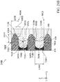
- FIG. 1A is a three-dimensional (3D) perspective view of an embodiment of a nano-sheet-based transistor that may be implemented as a PMOS and/or an NMOS in embodiments of nano-sheet-based CMOS devices of the present disclosure constructed according to some embodiments of the present disclosure.
- FIG. 1B is a cross-sectional view of an embodiment of a nano-sheet-based transistor that may be implemented as a PMOS and/or an NMOS in embodiments of nano-sheet-based CMOS devices of the present disclosure along the line A-A′ in FIG. 1A constructed according to some embodiments of the present disclosure.
- FIGS. 2A-2D are flow charts of embodiments of methods for fabricating nano-sheet-based CMOS devices of the present disclosure according to some embodiments of the present disclosure.
- FIGS. 3, 4, 5, 6, 7, 8, 9, 10, 11, 12, 13, 14, 15, 16, 17, 18, 19, 20, 21A, 21B, 22 , 23 , 24 , 25 , 26 , 27 , 28 A, and 28 B are cross-sectional views of an embodiment of a PMOS and an embodiment of an NMOS in embodiments of nano-sheet-based CMOS devices of the present disclosure along the line A-A′ in FIG. 1A constructed at various fabrication stages according to some embodiments of the present disclosure.
- first and second features are formed in direct contact
- additional features may be formed between the first and second features, such that the first and second features may not be in direct contact
- present disclosure may repeat reference numerals and/or letters in the various examples. This repetition is for the purpose of simplicity and clarity and does not in itself dictate a relationship between the various embodiments and/or configurations discussed.
- spatially relative terms such as “beneath,” “below,” “lower,” “above,” “upper” and the like, may be used herein for ease of description to describe one element or feature's relationship to another element(s) or feature(s) as illustrated in the figures.
- the spatially relative terms are intended to encompass different orientations of the device in use or operation in addition to the orientation depicted in the figures.
- the apparatus may be otherwise oriented (rotated 90 degrees or at other orientations) and the spatially relative descriptors used herein may likewise be interpreted accordingly.
- CMOS complementary metal-oxide-semiconductor
- PMOS p-type transistors
- NMOS n-type transistors
- CMOS technology is used for constructing microprocessors, memory chips, microcontrollers, among others.
- technologies progress towards smaller technology nodes (for example, 20 nm, 16 nm, 10 nm, 7 nm, 5 nm, and below)
- the optimization of CMOS performance increasingly hinges on reducing chip footprint and balancing performance characteristics of PMOS and NMOS transistors.
- nano-sheet-based transistors have become a popular and promising architecture for building CMOS devices.
- the present disclosure provides methods of fabricating nano-sheet-based CMOS transistors. Particularly, the methods of the present disclosure decouple the fabrications of PMOS and NMOS transistors such that these different types of devices may be separately tuned for the optimal overall performance of the nano-sheet-based CMOS devices.
- inner spacers of the PMOS and NMOS transistors of the present disclosure are made to have different physical dimensions, different surface profiles, and/or different material compositions such that the performance of the PMOS and NMOS devices can be separately tuned.
- a nano-sheet-based device includes any device that has a plurality of suspended gate channel layers stacked together to form the gate structure.
- Nano-sheet-based devices include gate-all-around (GAA) devices, multi-bridge-channel (MBC) devices, and other similar devices.
- the nano-sheet-based devices may include gate channel layers of any suitable shapes and/or configurations.
- the gate channel layers may be in one of many different shapes, such as wire (or nanowire), sheet (or nanosheet), bar (or nano-bar), and/or other suitable shapes.
- the term nano-sheet-based devices broadly encompasses devices having gate channel layers in nanowire, nano-bars, and any suitable shapes.
- MOSFETs metal-oxide semiconductor field effect transistors
- planar MOSFETs planar MOSFETs
- FinFETs other multi-gate FETs
- FIGS. 1A and 1B An exemplary nano-sheet-based transistor 100 is illustrated in FIGS. 1A and 1B .
- FIG. 1A is a three-dimensional (3D) perspective view of an embodiment of a nano-sheet-based transistor that may be implemented as a PMOS and/or an NMOS transistor in embodiments of nano-sheet-based CMOS devices of the present disclosure.
- FIG. 1B is a cross-sectional view of the nano-sheet-based transistor in FIG. 1A along the line A-A′.
- the nano-sheet-based transistor 100 includes a semiconductor substrate 105 . Fin structures (or fins), such as fin structures 108 , are formed over the substrate 105 , each extending lengthwise horizontally in an X-direction and separated from each other horizontally in a Y-direction.
- the X-direction and the Y-direction are horizontal directions that are perpendicular to each other, and that the Z-direction is a vertical direction that is orthogonal (or normal) to a horizontal XY plane defined by the X-direction and the Y-direction.
- the semiconductor substrate 105 may have its top surface parallel to the XY plane.
- the fin structures 108 each have a source region, a drain region (collectively, source/drain regions 102 , or, source and drain regions 102 ) disposed along the X-direction and spaced away from each other.
- Epitaxial source/drain features 210 are formed in the source/drain regions 102 .
- the fin structures 108 each further have a channel region 104 disposed between and connecting the source and drain regions 102 .
- a stack of suspended semiconductor layers 120 also referred to as “channel layers 120 ”) are formed in the channel region 104 connecting the epitaxial source/drain features 210 ; and the stack extends vertically (e.g. along the Z-direction) from the substrate 105 .
- the suspended semiconductor layers 120 may each be in one of many different shapes, such as wire (or nanowire), sheet (or nanosheet), bar (or nano-bar), and/or other suitable shapes, and may be spaced away from each other. In the depicted embodiments, there are three semiconductor layers 120 in the stack. However, there may be any appropriate number of layers in the stack, such as 2 to 10 layers.
- the semiconductor layers 120 may each engage with a single, contiguous gate structure 250 . Note that the gate structure 250 is illustrated as a transparent feature in FIG. 1A in order to illustrate the features (such as the semiconductor layers 120 ) that the gate structure 250 covers.
- the nano-sheet-based transistor 100 further includes isolation features 150 within and/or over the substrate 105 , separating adjacent fin structures from each other.
- the isolation features 150 may be shallow trench isolation (STI) features.
- the formation of the isolation features 150 includes etching trenches into the substrate 105 between the active regions (the regions in which the fin structures are formed) and filling the trenches with one or more dielectric materials such as silicon oxide, silicon nitride, silicon oxynitride, other suitable materials, or combinations thereof.
- the isolation features 150 may have a multi-layer structure such as a thermal oxide liner layer over the substrate 105 and a filling layer (e.g., silicon nitride or silicon oxide) over the thermal oxide liner layer.
- the isolation features 150 may be formed using any other isolation technologies. As illustrated in FIG.
- the fin structure 108 is located above the top surface of the isolation features 150 .
- the nano-sheet-based transistor 100 further includes gate spacer layers 200 on both sides of the gate structure 250 ; optionally gate spacer layers 202 on two sides of the gate spacer layers 200 ; optionally contact etch stop layers 220 over the epitaxial source/drain features 210 ; interlayer dielectric (ILD) layer 230 over the epitaxial source/drain features 210 (and over the contact etch stop layers 220 , if present); and optionally source/drain spacers 207 over the isolation features 150 .
- ILD interlayer dielectric
- FIGS. 2A-2D are flow charts illustrating two embodiments of a method 10 for fabricating a nano-sheet-based CMOS device of the present disclosure according to some embodiments of the present disclosure.
- the first embodiment of method 10 (denoted as embodiment 10 A) and the second embodiment of method 10 (denoted as embodiment 10 B) share the same processing steps 12 - 30 , illustrated in FIGS. 2A and 2B .
- the embodiment 10 A continues from step (or block) 30 to 32 A and through 46 A, as illustrated in FIG. 2C .
- the embodiment 10 B continues from step (or block) 30 to 32 B and through 44 B, as illustrated in FIG. 2D .
- FIGS. 22-27, 28A, and 28B are cross-sectional views of a nano-sheet-based CMOS device along the line A-A′ in FIG. 1A constructed at various fabrication stages according to the embodiment 10 B of method 10 .
- the nano-sheet-based CMOS includes a substrate 105 .
- the substrate 105 contains a semiconductor material, such as bulk silicon (Si), germanium (Ge), silicon germanium (SiGe), silicon carbide (SiC), gallium arsenic (GaAs), gallium phosphide (GaP), indium phosphide (InP), indium arsenide (InAs), and/or indium antimonide (InSb), or combinations thereof.
- the substrate 105 may also include a semiconductor-on-insulator substrate, such as Si-on-insulator (SOI), SiGe-on-insulator (SGOI), Ge-on-insulator (GOI) substrates.
- SOI Si-on-insulator
- SGOI SiGe-on-insulator
- GOI Ge-on-insulator
- Some regions of the substrate 105 may be doped.
- a region configured for a PMOS transistor of the nano-sheet-based CMOS may be doped with n-type dopants, such as phosphorus (P) and/or arsenic (As);
- a region configured for an NMOS transistor of the nano-sheet-based CMOS may be doped with p-type dopants, such as boron (B) and/or boron fluoride (BF 3 ).
- the doped regions may be formed directly on the substrate 105 , in a p-well structure, in an n-well structure, in a dual-well structure, or using a raised structure.
- stacks of semiconductor layers are formed over the substrate 105 to later form the PMOS transistor 100 A and the NMOS transistor 100 B.
- the stacks of semiconductor layers include semiconductor layers 110 and semiconductor layers 120 alternating with each other.
- a semiconductor layer 110 is formed over the substrate 105 ;
- a semiconductor layer 120 is formed over the semiconductor layer 110 ;
- another semiconductor layer 110 is formed over the semiconductor layer 120 , so on and so forth.
- the material compositions of the semiconductor layers 110 and 120 are configured such that they have an etching selectivity in a subsequent etching process.
- the semiconductor layers 110 contain silicon germanium (SiGe), while the semiconductor layers 120 contain silicon (Si).
- the semiconductor layers 120 contain SiGe, while the semiconductor layers 110 contain Si.
- the semiconductor layers 110 each have a substantially uniform thickness, referred to as the thickness 300
- the semiconductor layers 120 each have a substantially uniform thickness, referred to as the thickness 310 .
- the thickness 310 may be the same as, or different from, the thickness 300 .
- the stacks of semiconductor layers are patterned into a plurality of fin structures, for example, fin structures 108 A and 108 B, such that they each extend along the X-direction.
- the fin structures 108 A and 108 B may be patterned by any suitable method.
- the fins may be patterned using one or more photolithography processes, including double-patterning or multi-patterning processes.
- double-patterning or multi-patterning processes combine photolithography and self-aligned processes, allowing patterns to be created that have, for example, pitches smaller than what is otherwise obtainable using a single, direct photolithography process.
- a sacrificial layer is formed over a substrate and patterned using a photolithography process.
- Spacers are formed alongside the patterned sacrificial layer using a self-aligned process.
- the sacrificial layer is then removed, and the remaining spacers, or mandrels, may then be used to pattern the fins.
- the patterning may utilize multiple etching processes which may include a dry etching and/or wet etching.
- the fin structures 108 A and 108 B may have lateral widths (not shown) along the Y-direction that are the same between each other or different from each other.
- dummy gate structures 240 are formed over a portion of each of the fin structures 108 A and 108 B. In some embodiments, the dummy gate structures are also formed over the isolation features 150 in between adjacent fin structures.
- the dummy gate structures 240 may be configured to extend lengthwise in parallel to each other, for example, each along the Y-direction. In some embodiments, the dummy gate structures each wrap around the top surface and side surfaces of each of the fin structures 108 A and 108 B.
- the dummy gate structures 240 may include polysilicon. In some embodiments, the dummy gate structures 240 also include one or more mask layers (not shown), which are used to pattern the dummy gate electrode layers.
- the dummy gate structures 240 may undergo a gate replacement process through subsequent processing to form metal gates, such as a high-k metal gate, as discussed in greater detail below.
- the dummy gate structures 240 may be formed by a procedure including deposition, lithography, patterning, and etching processes.
- the deposition processes may include CVD, ALD, PVD, other suitable methods, and/or combinations thereof.
- Gate spacers are formed on the sidewalls of the dummy gate structures 240 and the top layer of the semiconductor layers 120 .
- Gate spacers may include a single layer or a multi-layer structure.
- a gate spacer layer 200 is formed over the top surface of the device, and a gate spacer layer 202 is formed over the gate spacer layer 200 .
- the gate spacer layers 200 and 202 may each include silicon nitride (Si 3 N 4 ), silicon oxide (SiO 2 ), silicon carbide (SiC), silicon oxycarbide (SiOC), silicon oxynitride (SiON), silicon oxycarbon nitride (SiOCN), carbon doped oxide, nitrogen doped oxide, porous oxide, or combinations thereof.
- the gate spacer layers 200 and 202 may collectively has a thickness in the range of a few nanometers (nm).
- the gate spacer layers 200 and/or 202 may be formed by depositing a spacer layer (containing the dielectric material) over the dummy gate structures 240 , followed by an anisotropic etching process to remove portions of the spacer layer from the top surfaces of the dummy gate structures 240 . After the etching process, portions of the spacer layer on the sidewall surfaces of the dummy gate structures 240 substantially remain and become the gate spacer layers 200 and/or 202 .
- the anisotropic etching process is a dry (e.g. plasma) etching process. Additionally or alternatively, the formation of the gate spacer layers 200 and/or 202 may also involve chemical oxidation, thermal oxidation, ALD, CVD, and/or other suitable methods.
- Processing continues to selectively process the region configured for the PMOS transistor 100 A, while leaving the region configured for the NMOS transistor 100 B unaffected.
- a mask layer 350 is formed to cover the region configured for the NMOS transistor 100 B while leaving the region configured for the PMOS transistor 100 A open. Accordingly, subsequent processing affects only the region configured for the PMOS transistor 100 A.
- portions of the fin structure 108 A adjacent to and exposed by the dummy gate structures 240 are at least partially recessed (or etched away) by process 500 A to form the source/drain trenches 204 A.
- the process 500 A removes not only the exposed portions of fin structure 108 A, but also a portion of the underlying substrate 105 . Accordingly, the source/drain trenches 204 A extends below the top surface of the substrate 105 . In some embodiments (not shown), the process 500 A removes only the exposed portions of the fin structure 108 A, such that the top surface of the substrate 105 is exposed in the source/drain trenches 204 A.
- the source/drain trenches 204 A extends to a depth along the top surface of the substrate 105 .
- the process 500 A removes only some, but not all, of the fin structure 108 A adjacent the dummy gate structures 240 , such that the substrate 105 is not exposed in the source/drain trenches 204 A. Accordingly, the source/drain trenches 204 A extends to a depth above the top surface of the substrate 105 .
- the process 500 A may include multiple lithography and etching steps, and may use any suitable methods, such as dry etching and/or wet etching.
- the formation of the source/drain trenches 204 A exposes sidewalls of the stack of semiconductor layers 110 and 120 in the region configured for the PMOS transistor 100 A.
- portions of the semiconductor layers 110 are removed through the exposed sidewall surfaces in the source/drain trenches 204 A via a selective etching process, such as process 520 A.
- the process 520 A is designed to remove portions of the semiconductor layers 110 but only minimally affect the semiconductor layers 120 .
- two side portions of the semiconductor layers 110 may be removed to form openings 205 while the side portions of the semiconductor layers 120 directly above and below the openings 205 are substantially preserved.
- those side portions of the semiconductor layers 120 may have their thicknesses reduced by about 1% to about 10% during the process 520 A.
- the selective etching process may be any suitable processes.
- the semiconductor layers 120 include Si and the semiconductor layers 110 include SiGe.
- the process 520 A may be a wet etching process, such as a Standard Clean 1 (SC-1) solution.
- SC-1 solution includes ammonia hydroxide (NH 4 OH), hydrogen peroxide (H 2 O 2 ), and water (H 2 O).
- the SiGe semiconductor layers 110 may be etched away in the SC-1 solution at a substantially faster rate than the Si semiconductor layers 120 .
- the etching duration is adjusted such that the size of the removed portions of SiGe layers is controlled.
- desired portions of the semiconductor layers 110 are removed while the semiconductor layers 120 are only minimally affected.
- the optimal condition may be reached by additionally adjusting the etching temperature, dopant concentration, as well as other experimental parameters.
- the semiconductor layers 120 include SiGe and the semiconductor layers 110 includes Si.
- a cryogenic deep reactive ion etching (DRIE) process may be used to selectively etch away the Si semiconductor layer 110 .
- the DRIE process may implement a sulfur hexafluoride-oxygen (SF 6 —O 2 ) plasma.
- the optimal condition may be reached by adjusting the etching temperature, the power of the Inductively Coupled Plasma (ICP) power source and/or Radio Frequency (RF) power source, the ratio between the SF 6 concentration and the O 2 concentration, the dopant (such as boron) concentrations, as well as other experimental parameters.
- ICP Inductively Coupled Plasma
- RF Radio Frequency
- the etching rate of a Si semiconductor layer 110 using a SF 6 —O 2 plasma may exceed about 8 ⁇ m/min at a temperature of about ⁇ 80° C.; while the SiGe semiconductor layers 120 are not substantially affected during the process.
- the openings 205 A formed during the process 520 A extend the source/drain trenches 204 A into areas beneath the semiconductor layers 120 and gate spacer layers 200 and/or 202 .
- the extent to which the semiconductor layers 110 are laterally recessed (or the size of the portion removed) is determined by the processing conditions such as the duration that the semiconductor layers 110 is exposed to an etching chemical.
- the duration is controlled such that the opening 205 A has a depth 330 A along the X-direction.
- the etching process conditions cause the openings 205 A to have curved surfaces. For example, as illustrated in FIG.
- the openings 205 A may have a curved interface (surface 410 ) with the remaining portions of the semiconductor layers 110 .
- the surface 410 protrudes from the openings 205 A into the semiconductor layers 110 .
- the openings 205 A may have a larger depth at its mid-height along the Z-direction than at its top or bottom interfaces with the semiconductor layers 120 .
- the depth 330 A represents the average depth of the opening 205 A.
- the depth 330 A determines the upper limit of the lateral widths of inner spacers to be formed within the openings 205 A. In some embodiments, the depth 330 A may be about 5.5 nm to about 11 nm.
- the sidewalls of the semiconductor layers 120 may also have curved surfaces. As described above, although the semiconductor layers 120 are largely preserved during the process 520 due to their etching resistance to the etching chemical, they nevertheless may have their thicknesses slightly reduced. In addition, their sidewalls may be altered. For example, prior to the process 520 A, the semiconductor layers 120 may have substantially straight side surfaces (see FIG. 5 ). But after the process 520 A, the semiconductor layers 120 may have rounded (or curved) surfaces. The surface profiles of the semiconductor layers 120 carry significances in affecting the quality of epitaxial source/drain features subsequently formed in the openings 205 A. This is described in more detail later.
- the semiconductor layers 120 each have a rounded surface 400 protruding into the source/drain trenches 204 A.
- the semiconductor layers 120 may have a larger length along the X-direction at its mid-height along the Z-direction than at its top or bottom interfaces with the semiconductor layers 110 (and the openings 205 ).
- the maximum length of the semiconductor layers 120 at their respective mid-height is about 20 nm to about 300 nm.
- a dielectric material 306 A is deposited into both the source/drain trenches 204 A and the openings 205 A.
- the dielectric material 306 A may be selected from SiO 2 , SiON, SiOC, SiOCN, or combinations thereof. In some embodiments, the proper selection of the dielectric material may be based on its dielectric constant (as described later).
- the deposition of the dielectric material 306 A may be any suitable methods, such as CVD, PVD, PECVD, MOCVD, ALD, PEALD, or combinations thereof. In the depicted embodiment, the dielectric material 306 A may have a top surface that extends along a top surface of the dummy gate structure 240 .
- the dielectric material 306 A may have a top surface that extends above the top surface of the dummy gate structure 240 , and a CMP process may be performed to planarize the top surfaces of the device, and to expose the top surfaces of the dummy gate structure 240 .
- the dielectric material 306 A is partially etched back by process 540 A to form new source/drain trenches 208 A.
- the partial etching-back completely removes the dielectric materials 306 A within the original source/drain trenches 204 A, and removes a portion, but not all, of the dielectric materials 306 A within the original openings 205 A (compare FIG. 6 ).
- the dielectric materials 306 A remaining in the openings 205 A become the inner spacers 206 A. Accordingly, the inner spacers 206 A are formed between vertically adjacent semiconductor layers 120 .
- the etching-back is a self-aligned anisotropic dry-etching process, such that the gate spacer layers 200 and/or 202 are used as the masking element.
- a different masking element e.g. a photoresist may be used.
- the inner spacers 206 A interface the remaining portions of the semiconductor layers 110 at the surface 410 . Additionally, the inner spacers 206 A have a new surface 420 exposed in the source/drain trenches 208 A. The distance between the surfaces 410 and 420 defines the lateral width 340 A of the inner spacers 206 A. The new surface 420 may be of a same or different profile as that of the surface 410 . When the surfaces 410 and 420 have different profiles, the inner spacers 206 A may have varying lateral widths at different heights of the inner spacers 206 A along the Z-direction. In such embodiments, the lateral width 340 A represents an average lateral width of the inner spacers 206 A.
- the lateral width 340 A is smaller than the depth 330 A of the opening 205 A.
- the lateral width 340 A is important to tuning the capacitance parameters; and the surface profiles are important to improving the quality of the epitaxial source/drain features subsequently formed.
- epitaxial source/drain features 210 A are formed in the source/drain trenches 208 A. Accordingly, the epitaxial source/drain features 210 A interface with the inner spacers 206 A at the surface 420 . Multiple processes, including etching and growth processes, may be employed to grow the epitaxial source/drain features 210 A. In the depicted embodiment, the epitaxial source/drain features 210 A have top surfaces that extend higher than the top surface of the topmost semiconductor layer 120 . However, in other embodiments, the epitaxial source/drain features 210 A may alternatively have top surfaces that are about even with the top surface of the topmost semiconductor layer 120 .
- the epitaxial source/drain features 210 A may merge together, for example, along the Y-direction (see e.g., FIG. 1A ), to provide a larger lateral width than an individual epitaxial source/drain feature.
- the epitaxial source/drain features 210 A are configured to be part of the PMOS transistor 100 A. Accordingly, the epitaxial source/drain features 210 A may include any suitable p-type semiconductor materials, such as Si, SiGe, Ge, SiGeC, or combinations thereof.
- the epitaxial source/drain features 210 A may be doped in-situ or ex-situ.
- the epitaxially grown SiGe source/drain features may be doped with boron.
- One or more annealing processes may be performed to activate the dopants in the epitaxial source/drain features 210 A.
- the annealing processes may comprise rapid thermal annealing (RTA) and/or laser annealing processes.
- each pair of epitaxial source/drain features 210 A are connected by multiple semiconductor layers 120 , which serve as the carrier conduit between the epitaxial source/drain features 210 A during the operation. Additionally, referring to FIG. 10 , the embodiments of method 10 optionally include forming a contact etch stop layers 220 A over the epitaxial source/drain features 210 A, as well as gate spacer layers 200 and/or 202 .
- Embodiments of method 10 continues to form components of the NMOS transistor 100 B.
- the mask layer 350 over the region configured for the NMOS transistor 100 B is removed, and a new mask layer 360 is formed over the region configured for the PMOS transistor 100 A. Accordingly, subsequent processing affects only the region configured for the NMOS transistor 100 B.
- the mask layer 360 may have a material the same as or different from that of the mask layer 350 .
- portions of the fin structure 108 B adjacent to and exposed by the dummy gate structures 240 are at least partially recessed (or etched away) by process 500 B to form the source/drain trenches 204 B for subsequent epitaxial source and drain growths.
- the recess process 500 B may be substantially similar to the process 500 A described above with respect to FIG. 5 . Accordingly, the source/drain trenches 204 B may extend to a depth that is above, along or below the top surface of the substrate 105 .
- the depth of the source/drain trenches 204 B may be the same as, greater than, or less than the depth of the source/drain trenches 204 A.
- the source/drain trenches may have different depths in order to accommodate for the different growth requirements in subsequent epitaxial deposition processes in different regions, and/or to effectuate different strains in the later-formed source/drain features based on design requirements.
- the portions of the fin structure 108 B underneath the dummy gate structures 240 remain intact. Additionally, the process 500 B exposes the sidewalls of the stack of semiconductor layers 110 and 120 . Referring to block 30 of FIG. 2B and FIG.
- portions of the semiconductor layers 110 are removed through the exposed sidewall surfaces in the source/drain trenches 204 B via a selective etching process, such as process 520 B, thereby forming openings 205 B between adjacent layers of the semiconductor layers 120 .
- the process 520 B removes a portion of semiconductor layers 110 that has a lateral width (or average lateral width) 330 B.
- the openings 205 B may have curved surfaces.
- the openings 205 B may have a curved interface (surface 440 ) with the remaining portions of the semiconductor layers 110 .
- the surface 440 protrudes from the openings 205 B into the semiconductor layers 110 .
- the openings 205 B may have a larger depth at its mid-height along the Z-direction than at its top or bottom interfaces with the semiconductor layers 120 .
- the depth 330 B represents the average depth of the opening 205 B.
- the side surfaces of the semiconductor layers 120 may be slightly etched during the process 520 B removing the semiconductor layers 110 .
- the semiconductor layers 120 may now have rounded (or curved surfaces).
- the semiconductor layers each have a rounded surface 430 protruding into the source/drain trenches 204 B.
- the portions of the semiconductor layers 120 directly above and below the openings 205 B may further has reduced thicknesses, as compared to before the process 520 B is performed. For example, these portions may have thicknesses that are about 1% to about 10% less than before the process 520 B is performed.
- the process 520 B may be any suitable processes.
- the processes 520 A and 520 B are the same method.
- both the processes 520 A and 520 B are SC-1 etching process.
- both the processes 520 A and 520 B are cryogenic DRIE processes.
- the processes 520 A and 520 B are different methods.
- process 520 A may employ an SC-1 wet etching to form the openings 205 A while process 520 B may employ a cryogenic DRIE process to form the openings 205 B.
- different etching methods result in different surface profiles, such that the profile of the surface 420 (of the openings 205 A) and the profile of the surface 440 (of the openings 205 B) are different from each other. The significances of the depths and the profiles of the surface 440 will be described in detail later.
- FIG. 2B and FIGS. 13-21 illustrate subsequent steps of embodiment 10 A of method 10
- FIG. 2C and FIGS. 23-29 illustrate subsequent steps of embodiment 10 B of method 10 .
- a dielectric material 306 B is deposited into both the source/drain trenches 204 B and the openings 205 B.
- the dielectric material 306 B may be selected from SiO 2 , SiON, SiOC, SiOCN, or combinations thereof.
- the dielectric material 306 B may be deposited by any suitable methods, such as those described above with respect to the dielectric material 306 A.
- the dielectric material 306 B may be the same material as, or a different material from, the dielectric material 306 A, depending on the design needs. In some embodiments, the proper selection of the dielectric material may be based on the dielectric constants.
- this dielectric material 306 B may have a dielectric constant lower than that of the dielectric material 306 A. In some other embodiments, this dielectric material 306 B may have a dielectric constant higher than that of the dielectric material 306 A. This aspect of the dielectric material 306 A will be further discussed later.
- the dielectric material 306 B is etched back in process 540 B to form inner spacers 206 B.
- the formation of the inner spacers 206 B share many similar aspects as the formation of inner spacers 206 A (see description above with respect to FIG. 8 ).
- the process 540 B also forms new source/drain trenches 208 B (similar to the source/drain trenches 208 A described above); the inner spacers 206 B have a lateral width 340 B (similar to the lateral width 340 A of the inner spacers 206 A); the inner spacers 206 B interface with the semiconductor layers 110 at the surface 440 (similar to the surface 410 of the inner spacers 206 A) and interface with the source/drain trenches 208 B at the surface 450 (similar to the surface 420 of the inner spacers 206 A).
- the process 540 B may use the same etching method as, or a different etching method from, that of the process 540 A.
- the process 540 B employs a different etching method as that of the process 540 A.
- the process 540 A may use a wet-etching method, while the process 540 B may use a dry-etching method; or the process 540 A may use a SC-1 wet etching method, while the process 540 B may use a standard clean-2 (SC-2) wet etching method.
- SC-2 standard clean-2
- different etching methods may produce different surface profiles.
- the surface 450 may have a different profile from that of the surface 420 .
- the surface 450 has a smaller curvature than the surface 420 .
- the lateral width 340 B may also differ from the lateral width 340 A of the inner spacers 206 A. The significances of the lateral widths and surface profiles are described in more details later.
- embodiment 10 A of the method 10 continues to form epitaxial source/drain features 210 B in the source/drain trenches 208 B. Accordingly, the epitaxial source/drain features 210 B interface with the inner spacers 206 B at the surface 450 .
- the epitaxial source/drain features 210 B generally resemble the epitaxial source/drain features 210 A, and may be formed by similar methods. However, the epitaxial source/drain features may include different dopants. In the depicted embodiment, the epitaxial source/drain features 210 B are configured for an NMOS transistor 100 B.
- the epitaxial source/drain features 210 are doped with n-type dopants in-situ or ex-situ with the epitaxial growth.
- the epitaxially grown Si source/drain features may be doped with carbon to form silicon:carbon (Si:C) source/drain features, phosphorous to form silicon:phosphor (Si:P) source/drain features, or both carbon and phosphorous to form silicon carbon phosphor (SiCP) source/drain features.
- an optional contact-etch stop layer 220 B may be formed over the epitaxial source/drain features 210 B.
- the mask layer 360 is removed from the region configured for the PMOS transistor 100 A, and an interlayer dielectric (ILD) layer 230 is formed over the epitaxial source/drain features 210 A and 210 B, as well as vertically over the isolation features 150 .
- the ILD layer 230 may also be formed in between the adjacent dummy gate structures 240 along the X-direction, and in between the adjacent source/drain features 210 A/ 210 B along the Y-direction.
- the ILD layer 230 may include a dielectric material, such as a high-k material, a low-k material, or an extreme low-k material.
- the ILD layer 230 may include SiO 2 , SiOC, SiON, or combinations thereof.
- the materials of the ILD layer 230 may be the same as or different from that of the mask layers 350 and/or 360 .
- the ILD layer 230 may include a single layer or multiple layers, and may be formed by a suitable technique, such as CVD, ALD, and/or spin-on techniques. After forming the ILD layer 230 , a CMP process may be performed to remove excessive ILD layer 230 and planarized the top surface of the ILD layer 230 .
- the ILD layer 230 provides electrical isolation between the various components of the PMOS transistors 100 A and NMOS transistor 100 B.
- the dummy gate structures 240 in the region configured for the PMOS transistor 100 A are selectively removed in process 560 A
- the dummy gate structures 240 in the region configured for the NMOS transistor 100 B are selectively removed in process 560 B.
- the removal of the dummy gate structures 240 creates gate trenches 242 A and 242 B, respectively, which expose the respective top surfaces and the side surfaces of the semiconductor stacks (along the Y direction).
- the processes 560 A and 560 B each may be selected from any suitable lithography and etching processes.
- the lithography process may include forming a photoresist layer (resist), exposing the resist to a pattern, performing a post-exposure bake process, and developing the resist to form a masking element, which exposes a region including the dummy gate structures 240 . Then, the dummy gate structures 240 are selectively etched through the masking element.
- the gate spacer layers 200 and/or 202 may be used as the masking element or a part thereof.
- the processes 560 A and 560 B may be the same or different processes, and may be performed at the same or different times. Accordingly, the gate trenches 242 A and 242 B may be formed at the same or different times.
- the remaining portions of the semiconductor layers 110 are selectively removed through the exposed side surfaces of the semiconductor layers 120 .
- the semiconductor layers 110 in the region configured for the PMOS transistor 100 A is removed in process 580 A; and the semiconductor layers 110 in the region configured for the NMOS transistor 100 B is removed in process 580 B.
- the semiconductor layers 120 may be slightly affected during the processes 580 A and 580 B.
- the thickness of the semiconductor layers 120 may be reduced by about 1% to about 10%.
- the removal of the remaining portions of the semiconductor layers 110 form suspended semiconductor layers 120 , as well as openings 244 A and 244 B, respectively, in between the vertically adjacent layers.
- the center portions of the semiconductor layers 120 each have exposed top and bottom surfaces. In other words, the center portions of each of the semiconductor layers 120 are now exposed circumferentially around the X-direction.
- the openings 244 A may have a length 600 A; and the openings 244 B may have a length 600 B.
- the surfaces of the openings 244 A and 244 B are curved. Accordingly, the openings 244 A and 244 B each have different lengths at different heights along the Z-direction. Therefore, the lengths 600 A and 600 B represent the average lengths of the openings 244 A and 244 B, respectively.
- the lengths 600 A and 600 B may be the same as, or different from, each other. This is described in more details below.
- the processes 580 A and 580 B may be any suitable etching processes. Further, the processes 580 A and 580 B may be the same or different processes, and may be performed at the same or different time. In addition to exposing top and bottom surfaces of the center portions of the semiconductor layers 120 , these processes also expose the sidewall surfaces of the inner spacers 206 A and 206 B respectively. The exposed sidewall surfaces may or may not have been modified by the processes 580 A and 580 B.
- the process 580 A exposes surface 460 of the inner spacer 206 A. The surface 460 may be the same as, or different from, the surface 410 , depending on the choices of the etching methods and/or the materials of the inner spacers 206 A.
- the process 580 B exposes sidewall surface 470 of the inner spacer 206 B; and the surface 470 may be the same as, or different from, the surface 440 , depending on the choices of the etching methods and/or the materials of the inner spacers 206 B.
- a gate structure 250 A is formed in the openings 244 A and the gate trenches 242 A.
- a gate dielectric layer 246 A is formed over and between the semiconductor layers 120
- a conductive metal layer 248 A is formed over and between the portions of the gate dielectric layers 246 A.
- the gate dielectric layer 246 A includes multiple layers.
- the gate dielectric layer 246 A may include a high-k dielectric layer. The high-k gate dielectric layer may be formed conformally such that it at least partially fills the gate trenches 242 A.
- the high-k gate dielectric layer may be formed around the exposed surfaces of each of the semiconductor layers 120 , such that it wraps around each of the semiconductor layers 120 in 360 degrees.
- the high-k gate dielectric layer may further be formed over the side surfaces of the inner spacers 206 A, and the gate spacer layers 200 .
- the high-k gate dielectric layer may contain a dielectric material having a dielectric constant greater than a dielectric constant of SiO 2 , which is approximately 3.9.
- the high-k gate dielectric layer may include hafnium oxide (HfO 2 ), which has a dielectric constant in a range from about 18 to about 40.
- the high-k gate dielectric layer may include ZrO 2 , Y 2 O 3 , La 2 O 5 , Gd 2 O 5 , TiO 2 , Ta 2 O 5 , HfErO, HfLaO, HfYO, HfGdO, HfAlO, HfZrO, HfTiO, HfTaO, SrTiO, or combinations thereof.
- the formation of the high-k gate dielectric layers may be by any suitable processes, such as CVD, PVD, ALD, or combinations thereof.
- the gate dielectric layer 246 A further includes an interfacial layer.
- the interfacial layer is formed between the semiconductor layers 120 and the high-k dielectric layer. Any suitable methods may be used to form the interfacial layer, such as ALD, CVD, or other deposition methods. Alternatively, the interfacial layer may also be formed by an oxidation process, such as thermal oxidation or chemical oxidation. In this instance, no interfacial layer is formed on the sidewalls of the inner spacers 206 A or the gate spacer layers 200 . In many embodiments, the interfacial layer improves the adhesion between the semiconductor substrate and the subsequently formed high-k dielectric layer. However, in some embodiments, the interfacial layer is omitted.
- the conductive metal layer 248 A is formed over the gate dielectric layer 246 A and fills the remaining spaces of the gate trenches 242 A and the openings 244 A.
- the conductive metal layer 248 A may include a work function metal layer.
- the conductive metal layer 248 A is configured for the PMOS transistor 100 A.
- the work function metal layer may include any suitable p-type work function metal materials, such as titanium nitride (TiN), ruthenium (Ru), iridium (Jr), osmium (Os), rhodium (Rh), or combinations thereof.
- the conductive metal layer 248 A may further include a fill metal layer.
- the fill metal layer may include any suitable materials, such as aluminum (Al), tungsten (W), copper (Cu), cobalt (Co), nickel (Ni), platinum (Pt), ruthenium (Ru), or combinations thereof.
- a CMP is performed to expose a top surface of the ILD layer 230 .
- the gate dielectric layer 246 A and the conductive metal layer 248 A collectively form the gate structure 250 A.
- the gate structure 250 A engages multiple semiconductor layers 120 to form multiple gate channels.
- the multiple gate channels each have a channel length (or an average channel length) that is the same as the length 600 A of the openings 244 A. Accordingly, the length 600 A is also referred to as the channel length 600 A.
- a gate structure 250 B is formed in the openings 244 B and the gate trenches 242 B.
- the gate structure 250 B may have similar structures as gate structure 250 A.
- the gate structure 250 B may include a gate dielectric layer 246 B and a conductive metal layer 248 B.
- the gate dielectric layer 246 B may include a high-k dielectric layer (e.g., HfO 2 ) and an interfacial layer.
- the conductive metal layer 248 B may include a work function metal layer and a fill metal layer. In the depicted embodiment, the conductive metal layer 248 B is configured for the NMOS transistor 100 B.
- the work function metal layer may include any suitable n-type work function metal materials, such as titanium (Ti), aluminum (Al), tantalum (Ta), titanium aluminum (TiAl), titanium aluminum nitride (TiAlN), tantalum carbide (TaC), tantalum carbide nitride (TaCN), tantalum silicon nitride (TaSiN), or combinations thereof.
- the fill metal layer may include any suitable materials such as Al, W, Cu, Co, Ni, Pt, Ru, or combinations thereof.
- the gate structure 250 B engages multiple semiconductor layers 120 to form multiple gate channels.
- the multiple gate channels each have a channel length (or an average channel length) that is substantially the same as the length 600 B of the openings 244 B. Accordingly, the length 600 B is also referred to as the channel length 600 B.
- the length 600 B may be the same as, or different from, the length 600 A.
- the inner spacers 206 A and the inner spacers 206 B may have the same or different materials, the same or different lateral widths, and the same or different surface profiles; and the PMOS transistor 100 A may have the same or different gate channel lengths as the NMOS transistor 100 B.
- the materials and the lateral widths of the inner spacers may be tuned to achieve overall balanced capacitance of the nano-sheet-based CMOS; the gate channel lengths of may be tuned to achieve overall balanced current of the nano-sheet-based CMOS; and the surface profiles of the inner spacers may be tuned to optimize the qualities of the epitaxial source/drain features.
- a nano-sheet-based CMOS device includes various device regions that may be considered as capacitors.
- the inner spacers 206 A may be considered to be the dielectric medium of a capacitor between a pair of vertically aligned conductive plates, i.e., the sidewall of the epitaxial source/drain feature 210 A and the sidewall of the gate structure 250 A. This is denoted as region 260 A in FIG. 20 .
- the inner spacers 206 B may be considered to be the dielectric medium of another capacitor between another pair of vertically aligned conductive plates, i.e., the sidewall of the epitaxial source/drain feature 210 B and the sidewall of the gate structure 250 B.
- region 260 B This is denoted as region 260 B in FIG. 20 .
- the optimal performance of the nano-sheet-based CMOS device may be reached when the capacitances of the regions 260 A and 260 B are balanced. Balancing the capacitances require separately tuning parameters for each of the capacitors.
- the capacitance is proportional to the dielectric constant of the dielectric medium, and is inversely proportional to the separation distance of plates, according to the following equation:
- C the capacitance of the capacitor
- c the permittivity of the dielectric medium
- ⁇ 0 the permittivity of vacuum
- A the area of the plates
- d the separation distance of the plates
- k the dielectric constant of the dielectric medium. Therefore, a smaller dielectric constant leads to a smaller capacitance; and a smaller separation distance leads to larger capacitance.
- the method of the present disclosure provides the flexibility of forming inner spacers of different material compositions and/or lateral widths, such that the regions 260 A and 260 B may be individually optimized for the overall optimized performances of the nano-sheet-based CMOS.
- the inner spacers 206 A has a lateral width 340 A of about 5 nm to about 7 nm. If the lateral width is too small, such as less than 5 nm, the protection provided to the epitaxial source/drain features 210 A in subsequent etching processes may be insufficient; if the lateral width is too large, such as greater than 7 nm, the additional cost of chip footprint may not be worth the performance enhancement.
- the inner spacers 206 B has a lateral width 340 B of about 0.5 nm to about 5 nm.
- the inner spacer 205 A has a lateral width 340 A that may be equal to or greater than the lateral width 340 B of inner spacer 206 B by up to about 6.5 nm. If the lateral width is too small, such as less than 0.5 nm, the inner spacer dimension may suffer poor reliability; if the lateral width is too large, such as greater than 6.5 nm, it may be too close to the lateral width of the inner spacer 206 A, such that a balance of capacitance may not be reached.
- the inner spacers 206 A includes a dielectric material that has a dielectric constant smaller than the dielectric material of the inner spacers 206 B.
- a ratio of the lateral width 340 A to the lateral width 340 B may be about 14 to 1.1. If the ratio is too small, such as less than 1.1, the benefit afforded by the balanced capacitance may not justify the extra manufacturing cost associated with fabricating the asymmetric inner spacer structures; if the ratio is too large, such as greater than 14, either device 100 A will have to occupy unnecessarily large chip space or the device 100 B would suffer fabrication challenges due to its small inner spacer dimension.
- the optimal performance of the nano-sheet-based CMOS also requires overall balanced current flow.
- a PMOS transistor of a nano-sheet-based CMOS employs holes as the charge carriers
- an NMOS transistor of the same nano-sheet-based CMOS employs electrons as the charge carriers. Because the holes have much smaller mobility than the electrons, a shorter migration path (and therefore a shorter channel length) in the PMOS transistor than that in the NMOS transistor may be required in order to reach the same current flow level, thereby maximizing the maximum available drain current (I on ).
- the channel length 600 A of the PMOS transistor 100 A is about 5 nm to about 15 nm.
- the channel length 600 B of the NMOS transistor 100 B is about 10 nm to about 20 nm. In an embodiment, the channel length 600 B is greater than the channel length 600 A by about 5 nm to about 10 nm.
- a ratio of the channel length 600 B to the channel length 600 A may be about 1.3 to 4.
- the ratio is too small, the benefit afforded by the balanced current may not justify the extra manufacturing cost associated with fabricating the asymmetric inner spacer structures; if the ratio is too large, such as greater than 4, either device 100 B will have to occupy unnecessarily large chip space or the device 100 A would suffer fabrication challenges (such as forming gate components) due to its small channel dimension.
- FIG. 21A and FIG. 21B are expanded cross-sectional views of the regions 260 A and 260 B, respectively, illustrating the dimensions of the surface profiles.
- each of the semiconductor layers 120 in the region 260 A have the same surface profile, such as the profile for the surface 400 .
- the semiconductor layers 120 may each further have a flat portion of the outer surface, denoted as the portion 800 A.
- the surface 400 separates from the portion 800 A at the separation point 700 A.
- the separation point 700 A is part of a separation line that extends along the Y-direction.
- the surface 400 also has a tip point 710 A.
- the horizontal distance along the X-direction between the tip point 710 A and the separation point 700 A of the same semiconductor layer 120 is the maximum lateral width 610 A of the surface 400 .
- the maximum lateral width 610 A is about 0.5 nm to about 4.0 nm.
- the vertical distance along the Z-direction between the tip point 710 A and the separation point 700 A of the same semiconductor layer 120 is about half of the thickness 620 A of the semiconductor layer 120 .
- the thickness 620 A is about 3 nm to about 8 nm.
- the semiconductor layer 120 interfaces with the inner spacer 206 A at the interface point 730 A.
- the interface point 730 A is part of an interface line that extends between the semiconductor layer 120 and the inner spacers 206 A along the Y-direction.
- the semiconductor layer 120 also interfaces the epitaxial source/drain features 210 A at the same interface point 730 A. As illustrated, the semiconductor layers 120 each protrude into the epitaxial source/drain features 210 A. For example, referring back to FIG. 8 , the process 540 A may etch away proper amount of the dielectric material 306 A, such that the semiconductor layers 120 A each extend more towards the source/drain trenches 208 A.
- the horizontal distance 630 A between the tip point 710 A and the interface point 730 A represent the extent the semiconductor layers 120 protrudes into the epitaxial source/drain features as compared to the inner spacers 206 A. It is understood that a proper horizontal distance 630 A improves growth condition for the epitaxial source/drain feature 210 A.
- epitaxial source/drain features are known to grow on semiconductor substrates but not on dielectric materials (such that the dielectric materials of the inner spacers 206 A). Accordingly, the curved portion of the semiconductor layers 120 protruding into the source/drain trenches 208 A provide a larger surface area for improved epitaxial growths.
- the horizontal distance 630 A may be about 0.5 nm to about 2.0 nm.
- the tip point 710 A and the interface point 730 A define a portion of the surface 400 denoted as 810 A.
- the curvature of the portion 810 A may be described by the vertical separation distance 640 A between the portion 810 A and the portion 800 A along the Z-direction at the midpoint position along the X-direction between the tip point 710 A and the interface point 730 A.
- the vertical separation distance 640 A is about 0.2 nm to about 2.0 nm.
- the inner spacer 206 A may have a curved surface 420 facing the epitaxial source/drain features 210 A.
- the surface 420 may have a tip point 740 A.
- the curvature of the surface 420 may be described by the horizontal distance 650 A along the X-direction between the interface point 730 A and the tip point 740 A, as compared to the thickness 670 A of the gate structure between the semiconductor layers 120 .
- the horizontal distance 650 A is less than about 2 nm.
- the thickness 670 A of the gate structure between the semiconductor layers 120 are largely determined by the thickness of the original semiconductor layer 110 . In other words, the thickness 670 A is similar to the thickness 300 .
- the process 580 A slightly etches away the semiconductor layer 120 . Therefore, the thickness 670 A is slightly greater than the thickness 300 .
- the thickness 670 A is about 1% to about 10% greater than the thickness 300 .
- the thickness 670 A is about 8 nm to about 15 nm.
- the inner spacer 206 A may also have a curved surface 460 facing the gate structure 250 A.
- the inner spacer 206 A may have a concave surface 460 protruding towards the gate structure 250 A along the X-direction.
- the gate structure has a concave end surface 460 that protrudes inwardly along the X-direction.
- the surface 460 interfaces with the portion 800 A at an interface point 720 A.
- the interface point 720 A may be part of an interface line that extends between the semiconductor layer 120 and the inner spacer 206 A along the Y-direction.
- the surface 460 may also have a tip point 750 A.
- the curvature of the surface 460 may be described by the horizontal distance 660 A along the X-direction between the interface point 720 A and the tip point 750 A, as compared to the thickness 670 A of the gate structure 250 A between the adjacent semiconductor layers. In an embodiment, the horizontal distance 660 A is less than about 2 nm.
- the curvature of the surface 460 may be the same as or different from the curvature of the surface 420 . When the curvatures are the same, the inner spacers 206 A has uniform lateral width 340 A across its height; when the curvatures are different, the inner spacers 206 A has varying lateral widths across its height along the Z-direction, and the lateral width 340 A represents the average lateral width.
- the portion 810 A and the surface 420 intersect at the interface point 730 A (or the interface line that extends through the interface point 730 A) and form an angle 900 A.
- the angle 900 A is greater than 90°.
- the inventors of the present disclosure have discovered that, when the angle 900 A is smaller than or about equal to 90°, it is difficult to properly fill the entire space between the portion 810 A and the surface 420 with epitaxial materials. Accordingly, voids (or seams) may be formed in that region.
- the present embodiment of the method 10 allows the angle 900 A to be greater than 90°.
- the profile of the surface 400 is at least partially determined by the process 520 A (see FIG. 6 ). As described above, although the semiconductor layers 120 have small etching rate during the process 520 A, the process 520 A nevertheless reshapes the profiles of the semiconductor layers 120 , resulting in the curved surface 400 . Accordingly, the profile of the surface 400 may be tuned by selecting the appropriate etching methods and adjusting etching parameters. For example, a wet etching process and/or a high-temperature chemical etching process may result in a more curved surface; while a low-temperature etching process may result in less curved surface.
- the semiconductor layers 120 may have curved surfaces 430
- the inner spacers 206 B may have curved surfaces 450 and 470 , interfacing with the epitaxial source/drain features 210 B and gate structure 250 B, respectively.
- the surfaces 430 , 450 , and 470 may have the same profile or different profiles between each other.
- the surfaces 430 , 450 , and 470 may have the same curvatures or different curvatures among them.
- the surface 430 may have the same curvature as, or different curvature from, that of the surface 400 ; the surface 450 may have the same curvature as, or different curvature from, that of the surface 420 ; the surface 470 may have the same curvature as, or different curvature from, that of the surface 460 .
- the surfaces 430 and 470 have the same curvature as the surfaces 400 and 460 , respectively. Accordingly, various aspects for these surfaces (such as denotations and dimensions) are similar between the regions 260 A and 260 B.
- the maximum lateral width 610 B may be about the same as the maximum lateral width 610 A; the thickness 620 B may be the same as the thickness 620 A; the semiconductor layers 120 in region 260 B also protrude into the epitaxial source/drain features 210 B as they protrude into the epitaxial source/drain features 210 A; the gate structure 250 B also has a concave end surface 470 that protrudes inwardly along the X-direction.
- the surface 450 has a different curvature from that of the surface 420 . This is described in more detail below.
- the inner spacer 206 B interfaces with the epitaxial source/drain feature 210 B at the surface 450 . Additionally, the inner spacer 206 B interfaces with the semiconductor layer 120 at the interface point 730 B. In some embodiments, the interface point 730 B is part of an interface line that extends between the semiconductor layer 120 and the inner spacers 206 B. In some embodiments, the semiconductor layer 120 also interfaces the epitaxial source/drain features 210 B at the same interface point 730 B.
- the surface 450 may have a tip point 740 B.
- the curvature of the surface 450 may be described by the horizontal distance 650 B along the X-direction between the interface point 730 B and the tip point 740 B of the same semiconductor layer 120 , as compared to the thickness 670 B of the gate structure 250 B between the adjacent semiconductor layers.
- the horizontal distance 650 B is less than about 2 nm.
- the horizontal distance 650 B is smaller than the horizontal distance 650 A, while the thickness 670 B of the gate structure between the channel layers is about the same as the thickness 670 A.
- the curvature of the surface 450 is smaller than the curvature of the surface 420 .
- the curvature of the surface 450 may be larger than or about equal to that of the surface 420 . Additionally, the curvature of the surface 450 is also smaller than the curvature of the surface 470 in the depicted embodiment. However, in other embodiments, the curvature of the surface 450 may be larger than or about equal to the curvature of the surface 470 .
- the distance between the surfaces 470 and 450 is the lateral width 340 B of the inner spacers 206 B.
- the lateral width 340 B represents the average lateral width of the inner spacers 206 B. In an embodiment, the lateral width 340 B is less than about 5 nm. Accordingly, the lateral width 340 B of the NMOS transistor 100 B may be smaller than the lateral width 340 A of the PMOS transistor 100 A.
- the portion 810 B (defined by the tip point 710 B and the interface point 730 B on the surface 430 ) and the surface 450 (the interface between the inner spacer 206 B and the epitaxial source/drain features 210 B) intersect at the interface point 730 B (or the interface line that extends through the interface point 730 B) and form an angle 900 B.
- the angle 900 B is greater than 90°. Accordingly, like the situation with respect to the angle 900 A, much of the difficulty in filling sharp angles with epitaxial semiconductor material is avoided, and no voids (or seams) are formed in the region spanning the angle 900 B.
- the profile of the surface 430 may be tuned during the process 520 B (see FIG. 6 ) by selecting the appropriate etching methods and adjusting etching parameters. For example, a wet etching process and/or a high temperature chemical etching process may result in a more curved surface, while low temperature etching process may result in a less curved surface. Accordingly, the curvature of the surface 430 as formed is smaller than the curvature of the surface 400 .
- FIG. 10 A of the method 10 The disclosure above describes the embodiment 10 A of the method 10 .
- the embodiment 10 B of the method 10 shares the same processing steps 12 - 30 of embodiment 10 A, as illustrated in FIG. 2A .
- FIG. 2C and FIGS. 22-27 illustrate processing steps 32 B- 44 B, which may be different from the embodiment 10 A.
- embodiment 10 B of the method 10 proceeds from the processing step 30 to 32 B and through 44 B. Because these subsequent steps 32 B- 44 B share many same or similar characteristics as the processing steps 32 A through 46 A already described above, the descriptions below are abbreviated for simplicity and conciseness.
- epitaxial source/drain features 210 B are formed in the source/drain trenches 204 B (illustrated in FIG. 12 ).
- a dielectric material 306 A is deposited into the source/drain trenches 204 B before forming the epitaxial source/drain features 210 A; and a portion of the dielectric material 306 A later forms the inner spacer 206 A.
- these steps are omitted in the embodiment 10 B. In other words, no inner spacer is formed in embodiment 10 B.
- the epitaxial source/drain features 210 B directly interface with the semiconductor layers 110 at the surface 440 .
- the epitaxial source/drain features 210 B here generally resemble the epitaxial source/drain features 210 B of embodiment 10 A (and resemble the epitaxial source/drain features 210 A except that they may be doped with an n-type dopant rather than a p-type dopant).
- the processing step of block 34 B of FIG. 2D resembles the processing step of 32 A of FIG. 2B .
- an optional contact etch stop layer 220 may be formed over the epitaxial source/drain features 210 B (see FIG. 23 ).
- processing steps 34 B- 44 B of FIG. 2C of embodiment 10 B generally resemble the processing steps 36 A- 46 A of FIG. 2B of embodiment 10 A.
- an ILD layer 230 is formed over both the regions configured for the PMOS transistor 100 A and the regions configured for the NMOS transistor 100 B (see block 34 B of FIG. 2D and FIG. 24 ); the dummy gate structures 240 are removed from both regions by processes 760 A and 760 B and forming the gate trenches 242 A and 242 B respectively (see FIG. 25 ); the remaining portions of the semiconductor layers 110 are removed from both regions by processes 780 A and 780 B and forming openings 244 A and 244 B, respectively (see block 36 B- 38 B of FIG. 2D and FIG. 26 ).
- the process 780 A is configured such that the process removes substantially all remaining portions of the semiconductor layers 110 without substantially affecting the inner spacers 206 A.
- the semiconductor material of the semiconductor layers 110 may be etched away at a substantially faster rate in the selected etching chemical than the dielectric material 306 A of the inner spacers 206 A.
- the etching selectivity largely determines the extent of etching on the PMOS side.
- the semiconductor layers 110 interface directly with the epitaxial source/drain features 210 B in the region configured for the NMOS transistor 100 B.
- the extent of etching there may be controlled by adjusting the duration of the etching.
- the process 780 B may result in a curved surface 480 .
- the curved surface 480 may face an opposite direction as the curved surface 440 (compare FIG. 22 ).
- the openings 244 B may have a width greater at the midpoint of its height along the Z-direction than at the topmost and at the bottommost height along the Z-direction.
- the curved surface 480 may include the semiconductor material of the semiconductor layers 110 , the semiconductor materials of the epitaxial source/drain features 210 B, or both.
- a small portion of the semiconductor layers 110 remain after the process 780 B.
- the entirety of the semiconductor layers 110 are removed, along with a small portion of the epitaxial source/drain features 210 B.
- the average length of the openings 244 B along the X-direction, denoted as 620 B, largely determines the channel length of the NMOS transistor 100 B, as described in more details below.
- a gate structure 250 A is formed in the openings 244 A and the gate trenches 242 A of the PMOS transistor 100 A; a gate structure 250 B is formed in the openings 244 B and the gate trenches 242 B of the NMOS transistor 100 B. Similar to the embodiment 10 A already discussed above, the gate structure 250 A includes a gate dielectric layer 246 A and a conductive metal layer 248 A; the gate structure 250 B includes a gate dielectric layer 246 B and a conductive metal layer 248 B. In some embodiments, these layers each include materials similar to or the same as those already described above in the context of the embodiment 10 A.
- the gate structure 250 A has a channel length 680 A.
- the channel length 680 A may be similar to, or same as, the length 600 A for embodiment 10 A.
- the gate structure 250 B has a channel length 680 B.
- the channel length 680 B may be similar to, or same as, the channel length 600 B for embodiment 10 A.
- the region 270 A includes a capacitor, similar to the region 260 A described above with respect to embodiment 10 A; however, the region 270 B does not include a similar capacitor, which is different from the region 260 B described above in the context of embodiment 10 A.
- the gate structure 250 B (including a conductive material) directly interfaces the epitaxial source/drain features 210 B (including another conductive material).
- the gate structure 250 B has an end concave surface 480 that protrudes outwardly, as opposed to inwardly for the gate structure 250 A, along the X-direction. It is understood that one purpose of the inner spacers is to protect the epitaxial source/drain features during subsequent processes (such as etching processes to form contact holes). However, the n-type doped epitaxial source/drain features 210 B may have a different sensitivity to such subsequent processes from the p-type doped epitaxial source/drain features 210 A.
- the p-type doped epitaxial source/drain features 210 A may be relatively easily etched (thereby damaged) in such subsequent processes; while the n-type doped epitaxial source/drain features 210 B may be more resistant to such subsequent processes under the same condition. Accordingly, in some embodiments, the inner spacers may not be necessary and can be omitted for the NMOS transistor 100 B.
- FIGS. 28A and 28B are expanded cross-sectional views of the regions 270 A and 270 B, respectively, illustrating the dimensions of the surface profiles.
- the region 270 A substantially resembles the region 260 A of embodiment 10 A; while the region 270 B differs from the region 260 B.
- the semiconductor layers 120 may have curved surfaces 400
- the inner spacers 206 A may have curved surfaces 420 and 460 , interfacing with the epitaxial source/drain features 210 A and gate structure 250 A, respectively.
- the surfaces 400 , 420 , and 460 may have the same profile or different profiles.
- the surfaces 400 , 420 , and 460 may have the same curvatures or different curvatures.
- each layer of the semiconductor layers 120 share the same surface profile as the surface 430 .
- the semiconductor layers 120 each have a flat portion of the outer surface, denoted as the portion 800 B.
- the surface 430 separates from the portion 800 B at the separation point 700 B.
- the separation point is part of a separation line that extends along the Y-direction.
- the surface 430 also has a tip point 710 B.
- the horizontal distance along the X-direction between the tip point 710 B and the separation point 700 B of the same semiconductor layer 120 is the maximum lateral width 610 B of the surface 430 .
- the maximum lateral width 610 B is about 0.5 nm to about 4.0 nm.
- the vertical distance along the Z-direction between the tip point 710 B and the separation point 700 B of the same semiconductor layer 120 is about half of the thickness 620 B of the semiconductor layer 120 .
- the thickness 620 B may be the same as the thickness 620 A.
- the thickness 620 A is about 3 nm to about 8 nm.
- the gate structure 250 B interfaces the semiconductor layers 120 B at the portion 800 B. Additionally, the gate structure 250 interfaces the epitaxial source/drain features 210 B at the surface 480 .
- the surface 480 and the portion 800 B diverge (or separate) from each other at the separation point 720 B.
- the separation point 720 B is part of a separation line that extend between the surface 480 and the portion 800 B along the Y-direction.
- the surface 480 has a tip point 740 B. The horizontal distance between the separation point 720 B and the tip point 740 B is the maximum lateral width 660 B of the surface 480 .
- the curvature of the surface 480 is described by the maximum lateral width 660 B as compared to the thickness 670 B of the gate structure 250 B. As illustrated, the semiconductor layers 120 protrude into the epitaxial source/drain features 210 B such that they each extend wider than the gate structures 250 B.
- the tip point 710 B and the separation point 720 B define a portion of the surface 430 denoted as 810 B.
- the curvature of the portion 810 B may be described by the vertical separation distance 640 B between the portion 810 B and the portion 800 B along the Z-direction at the midpoint position along the X-direction between the tip point 710 B and the separation point 700 B.
- the vertical separation distance 640 B is about 0.2 nm to about 2.0 nm.
- the gate structure 250 B may have a curved surface 480 facing the epitaxial source/drain features 210 B.
- the surface 480 may have a tip point 740 B.
- the curvature of the surface 480 may be described by the horizontal distance 660 B along the X-direction between the separation point 720 B and the tip point 740 B of the same semiconductor layer 120 , as compared to the thickness 670 B of the gate structure 250 B between the semiconductor layers 120 .
- the horizontal distance 660 B is less than about 2 nm.
- the thickness 670 B of the gate structure between the semiconductor layers 120 are largely determined by the thickness of the original semiconductor layer 110 . In other words, the thickness 670 B is similar to the thickness 300 and the thickness 670 A. In an embodiment, the thickness 670 B is about 8 nm to about 15 nm.
- the portion 800 B and the surface 480 intersect at the separation point 720 B and form an angle 900 B.
- the angle 900 B is less than 90°.
- the angle 900 B is partially determined by the profile of the surface 480 , which is at least partially determined by the process 780 B (see FIG. 26 ). Accordingly, the magnitude of the angle 900 B may be tuned by selecting the appropriate etching methods and adjusting etching parameters. For example, a wet etching process may result in more curved surface, while a gas phase chemical etching process may result in less curved surface.
- the disclosed method allows the PMOS transistor and the NMOS transistor of a nano-sheet-based CMOS device to include inner spacers of different materials, dimensions, and/or surface profiles.
- the disclosed method allows the PMOS transistor to include an inner spacer, while the NMOS transistor to not include an inner spacer.
- the PMOS and NMOS transistors are afforded great flexibility in tuning the parameters to optimize its performance in order to balance with each other. As a result, better capacitance balance and/or better current balance may be achieved for the nano-sheet-based CMOS device.
- the present disclosure provides methods that improve the performance, functionality, and/or reliability of nano-sheet-based transistors.
- the present disclosure is directed to a semiconductor device.
- the semiconductor device includes a semiconductor substrate, a first pair of source and drain features and a second pair of source and drain features over the semiconductor substrate, a first stack of semiconductor layers and a second stack of semiconductor layers, a first gate and a second gate.
- the first pair of source and drain features are p-type doped; and the second pair of source and drain features are n-type doped.
- the first stack of semiconductor layers connect the first pair of source and drain features along a first direction.
- the second stack of semiconductor layers connect the second pair of source and drain features along a second direction.
- the first gate has a first portion between vertically adjacent layers of the first stack of semiconductor layers.
- the second gate has a second portion between vertically adjacent layers of the second stack of semiconductor layers.
- the first portion has a first dimension along the first direction, and the second portion has a second dimension along the second direction.
- the second dimension is larger than the first dimension.
- the semiconductor device further includes a first inner spacer.
- the first inner spacer has a third dimension along the first direction and connects the first portion and one of the first pair of source and drain features.
- a layer of the first stack of semiconductor layers includes a region where a material of the layer, a material of the first inner spacer, and a material of the one of the first pair of source and drain features are interfaced with one another.
- the fourth dimension is smaller than the third dimension.
- the first dimension is about 5 nm to about 15 nm
- the second dimension is about 10 nm to about 20 nm
- the third dimension is about 5 nm to about 7 nm
- the fourth dimension is about 0.5 nm to about 5 nm.
- the first inner spacer includes a first material
- the second inner spacer includes a second material
- the second material is different from the first material.
- the first inner spacer has a first interface with the one of the first pair of source and drain features
- the second inner spacer has a second interface with the one of the second pair of source and drain features.
- the first interface has a first surface profile
- the second interface has a second surface profile.
- the second surface profile is different from the first surface profile.
- the first stack of semiconductor layers are stacked along a third direction perpendicular to the first direction.
- a first layer of the first stack of semiconductor layers has a rounded end portion and a middle portion.
- the rounded end portion protrudes from an edge of the first inner spacer into the one of the first pair of source and drain features along the first direction by a first length.
- the first length is about 0.5 nm to about 2 nm.
- the middle portion is in between and directly contacts two adjacent portions of the first gate.
- the rounded end portion has a first thickness along the third direction at the midpoint of the first length.
- the middle portion has a second thickness along the third direction.
- a first thickness difference between the first thickness and the second thickness is about 1 nm to about 4 nm.
- the second stack of semiconductor layers are stacked along a fourth direction perpendicular to the second direction.
- a second layer of the second stack of semiconductor layers has a rounded end portion and a middle portion.
- the rounded end portion protrudes from an edge of the second inner spacer into the one of the second pair of source and drain features along the second direction by a second length.
- the middle portion is in between and directly contacting two adjacent portions of the second gate.
- the rounded end portion has a third thickness along the fourth direction at the midpoint of the second length.
- the middle portion has a fourth thickness along the fourth direction.
- a second thickness difference between the third thickness and the fourth thickness is different from the first thickness difference.
- the present disclosure is directed to a method.
- a structure is received.
- the structure includes a semiconductor substrate, a first stack of first semiconductor layers and second semiconductor layers over the semiconductor substrate, a second stack of third semiconductor layers and fourth semiconductor layers over the semiconductor substrate, a first dummy gate structure over the first stack, and a second dummy gate structure over the second stack.
- the first semiconductor layers and the second semiconductor layers have different material compositions and alternate with one another within the first stack.
- the third semiconductor layers and the fourth semiconductor layers have different material compositions and alternate with one another within the second stack.
- a first portion of the first stack on two sides of the first dummy gate is removed to form a first pair of source/drain trenches, thereby exposing a pair of first side surface of the first stack.
- a first portion of the first semiconductor layers is removed from the exposed pair of first side surfaces to form first gaps.
- a first inner spacer is formed in the first gaps, where the first inner spacer has a first dimension along a direction connecting the first pair of source/drain trenches.
- a first pair of source/drain features are epitaxially grown in the first pair of source/drain trenches.
- a first portion of the second stack on two sides of the second dummy gate is removed to form a second pair of source/drain trenches, thereby exposing a pair of second side surfaces of the second stack.
- a first portion of the third semiconductor layers is removed from the exposed second side surfaces to form second gaps.
- a second inner spacer is formed in the second gaps, where the second inner spacer has a second dimension along a direction connecting the second pair of source/drain trenches. The second dimension is different from the first dimension.
- a second pair of source/drain features are epitaxially grown in the second pair of source/drain trenches.
- the first and the second dummy gate structures are removed to form a first gate trench over the first stack and a second gate trench over the second stack, respectively.
- the second portion of the first semiconductor layers are removed from the first gate trench.
- a second portion of the third semiconductor layers is removed from the second gate trench.
- a first gate electrode is formed in the first gate trench.
- a second gate electrode is formed in the second gate trench.
- the epitaxially growing of the first pair of source/drain features includes epitaxially growing the first pair of source/drain features and doping the first pair of source/drain features with an n-type dopant; the epitaxially growing of the second pair of source/drain features includes epitaxially growing the second pair of source/drain features and doping the second pair of source/drain features with a p-type dopant; and the forming of the second inner spacer includes forming the second inner spacer with the second dimension larger than the first dimension.
- the removing of the first portion of the first semiconductor layers includes removing with a first etching method; the removing the first portion of the third semiconductor layers includes removing with a second etching method.
- the second etching method differs from the first etching method.
- the forming of the second inner spacer includes forming the second inner spacer with a material different from a material of the first inner spacer.
- the forming of the second inner spacer includes forming the second inner spacer with a surface profile different from a surface profile of the first inner spacer.
- the epitaxially growing of the first pair of source/drain features includes growing on a first interface between the first inner spacer and a layer of the first semiconductor layers such that one of the first pair of source/drain features directly contacts the first interface; and the epitaxially growing of the second pair of source/drain features includes growing on a second interface between the second inner spacer and a layer of the third semiconductor layers such that one of the second pair of source/drain features directly contacts the second interface.
- the forming of the first gate electrode includes forming the first gate electrode in contact with surfaces of the first inner spacer, and the forming of the second gate electrode includes forming the second gate electrode in contact with surfaces of the second inner spacer.
- the present disclosure is directed to a method.
- a structure is received.
- the structure includes a semiconductor substrate, a first stack of first semiconductor layers and second semiconductor layers over the semiconductor substrate, a second stack of third semiconductor layers and fourth semiconductor layers over the semiconductor substrate, a first dummy gate structure over the first stack, and a second dummy gate structure over the second stack.
- the first semiconductor layers and the second semiconductor layers have different material compositions and alternate with one another within the first stack.
- the third semiconductor layers and the fourth semiconductor layers have different material compositions and alternate with one another within the second stack.
- a first portion of the first stack on two sides of the first dummy gate structure is removed to form a first pair of source/drain trenches, thereby exposing a pair of first side surfaces of the first stack.
- a first portion of the first semiconductor layers is removed from the exposed pair of first side surfaces to form first gaps.
- First inner spacers are formed in the first gaps.
- the first inner spacers each has a first dimension along a first direction connecting the first pair of source/drain trenches.
- a first pair of source/drain features are epitaxially grown in the first pair of source/drain trenches, such that the first pair of source/drain features each directly contacts with one of the first inner spacers.
- a first portion of the second stack on two sides of the second dummy gate structure is removed to form a second pair of source/drain trenches, thereby exposing a pair of second side surfaces of the second stack.
- a first portion of the third semiconductor layers is removed from the exposed pair of second side surfaces to form second gaps.
- a second pair of source/drain features are grown in the second pair of source/drain trenches, such that the second pair of source/drain features each directly contacts with a side surface of a second portion of the third semiconductor layers.
- the first and the second dummy gate structures are removed to form a first gate trench over the first stack and a second gate trench over the second stack, respectively.
- a second portion of the first semiconductor layers is removed from the first gate trench.
- the second portion of the third semiconductor layers is removed from the second gate trench.
- a first gate electrode is formed in the first gate trench.
- a second gate electrode is formed in the second gate trench.
- the forming of the first gate electrode includes forming a first concaved gate electrode end surface that protrudes inwardly along the first direction; and the forming of the second gate electrode includes forming a second concaved gate electrode end surface that protrudes outwardly along the first direction.
- the forming of the first gate electrode includes forming the first gate electrode in contact with surfaces of the first inner spacers, and the forming of the second gate electrode includes forming the second gate electrode in contact with surfaces of the second pair of source/drain features.
Landscapes
- Engineering & Computer Science (AREA)
- Chemical & Material Sciences (AREA)
- Physics & Mathematics (AREA)
- Nanotechnology (AREA)
- Manufacturing & Machinery (AREA)
- Condensed Matter Physics & Semiconductors (AREA)
- General Physics & Mathematics (AREA)
- Computer Hardware Design (AREA)
- Microelectronics & Electronic Packaging (AREA)
- Power Engineering (AREA)
- Crystallography & Structural Chemistry (AREA)
- Theoretical Computer Science (AREA)
- Mathematical Physics (AREA)
- Insulated Gate Type Field-Effect Transistor (AREA)
- Metal-Oxide And Bipolar Metal-Oxide Semiconductor Integrated Circuits (AREA)
Abstract
Description
wherein C is the capacitance of the capacitor, c is the permittivity of the dielectric medium, ε0 is the permittivity of vacuum, A is the area of the plates, d is the separation distance of the plates, and k is the dielectric constant of the dielectric medium. Therefore, a smaller dielectric constant leads to a smaller capacitance; and a smaller separation distance leads to larger capacitance. The method of the present disclosure provides the flexibility of forming inner spacers of different material compositions and/or lateral widths, such that the
Claims (20)
Priority Applications (4)
| Application Number | Priority Date | Filing Date | Title |
|---|---|---|---|
| US16/875,726 US11476166B2 (en) | 2019-07-30 | 2020-05-15 | Nano-sheet-based complementary metal-oxide-semiconductor devices with asymmetric inner spacers |
| TW109122728A TW202121685A (en) | 2019-07-30 | 2020-07-06 | Semiconductor device |
| CN202010667860.6A CN112310077A (en) | 2019-07-30 | 2020-07-13 | Semiconductor device with a plurality of semiconductor chips |
| US17/858,991 US20220352036A1 (en) | 2019-07-30 | 2022-07-06 | Nano-Sheet-Based Complementary Metal-Oxide-Semiconductor Devices with Asymmetric Inner Spacers |
Applications Claiming Priority (2)
| Application Number | Priority Date | Filing Date | Title |
|---|---|---|---|
| US201962880311P | 2019-07-30 | 2019-07-30 | |
| US16/875,726 US11476166B2 (en) | 2019-07-30 | 2020-05-15 | Nano-sheet-based complementary metal-oxide-semiconductor devices with asymmetric inner spacers |
Related Child Applications (1)
| Application Number | Title | Priority Date | Filing Date |
|---|---|---|---|
| US17/858,991 Division US20220352036A1 (en) | 2019-07-30 | 2022-07-06 | Nano-Sheet-Based Complementary Metal-Oxide-Semiconductor Devices with Asymmetric Inner Spacers |
Publications (2)
| Publication Number | Publication Date |
|---|---|
| US20210035870A1 US20210035870A1 (en) | 2021-02-04 |
| US11476166B2 true US11476166B2 (en) | 2022-10-18 |
Family
ID=74259412
Family Applications (2)
| Application Number | Title | Priority Date | Filing Date |
|---|---|---|---|
| US16/875,726 Active US11476166B2 (en) | 2019-07-30 | 2020-05-15 | Nano-sheet-based complementary metal-oxide-semiconductor devices with asymmetric inner spacers |
| US17/858,991 Pending US20220352036A1 (en) | 2019-07-30 | 2022-07-06 | Nano-Sheet-Based Complementary Metal-Oxide-Semiconductor Devices with Asymmetric Inner Spacers |
Family Applications After (1)
| Application Number | Title | Priority Date | Filing Date |
|---|---|---|---|
| US17/858,991 Pending US20220352036A1 (en) | 2019-07-30 | 2022-07-06 | Nano-Sheet-Based Complementary Metal-Oxide-Semiconductor Devices with Asymmetric Inner Spacers |
Country Status (3)
| Country | Link |
|---|---|
| US (2) | US11476166B2 (en) |
| CN (1) | CN112310077A (en) |
| TW (1) | TW202121685A (en) |
Families Citing this family (10)
| Publication number | Priority date | Publication date | Assignee | Title |
|---|---|---|---|---|
| US20210408285A1 (en) * | 2020-06-26 | 2021-12-30 | Intel Corporation | Gate-all-around integrated circuit structures having germanium-doped nanoribbon channel structures |
| US20220005951A1 (en) * | 2020-07-05 | 2022-01-06 | International Business Machines Corporation | Strained Semiconductor FET Devices with Epitaxial Quality Improvement |
| KR20220108561A (en) * | 2021-01-27 | 2022-08-03 | 삼성전자주식회사 | Semiconductor device |
| US20230018480A1 (en) * | 2021-07-16 | 2023-01-19 | Taiwan Semiconductor Manufacturing Company, Ltd. | Semiconductor device structure and method for forming the same |
| US20230037719A1 (en) * | 2021-08-08 | 2023-02-09 | Applied Materials, Inc. | Methods of forming bottom dielectric isolation layers |
| US20230063612A1 (en) * | 2021-08-31 | 2023-03-02 | Taiwan Semiconductor Manufacturing Company, Ltd. | Devices with improved operational current and reduced leakage current |
| CN118160084A (en) * | 2021-09-03 | 2024-06-07 | Imec 非营利协会 | Nanostructures comprising nanoplatelet or nanowire transistors |
| KR20230129697A (en) * | 2022-03-02 | 2023-09-11 | 삼성전자주식회사 | Semiconductor device |
| KR20230164831A (en) * | 2022-05-26 | 2023-12-05 | 삼성전자주식회사 | Semiconductor device |
| CN114914159B (en) * | 2022-06-16 | 2024-05-28 | 上海集成电路制造创新中心有限公司 | GAA transistor preparation method, device and equipment |
Citations (18)
| Publication number | Priority date | Publication date | Assignee | Title |
|---|---|---|---|---|
| US8772109B2 (en) | 2012-10-24 | 2014-07-08 | Taiwan Semiconductor Manufacturing Company, Ltd. | Apparatus and method for forming semiconductor contacts |
| US8785285B2 (en) | 2012-03-08 | 2014-07-22 | Taiwan Semiconductor Manufacturing Company, Ltd. | Semiconductor devices and methods of manufacture thereof |
| US8816444B2 (en) | 2011-04-29 | 2014-08-26 | Taiwan Semiconductor Manufacturing Company, Ltd. | System and methods for converting planar design to FinFET design |
| US8823065B2 (en) | 2012-11-08 | 2014-09-02 | Taiwan Semiconductor Manufacturing Company, Ltd. | Contact structure of semiconductor device |
| US8860148B2 (en) | 2012-04-11 | 2014-10-14 | Taiwan Semiconductor Manufacturing Company, Ltd. | Structure and method for FinFET integrated with capacitor |
| US9105490B2 (en) | 2012-09-27 | 2015-08-11 | Taiwan Semiconductor Manufacturing Company, Ltd. | Contact structure of semiconductor device |
| US9236267B2 (en) | 2012-02-09 | 2016-01-12 | Taiwan Semiconductor Manufacturing Company, Ltd. | Cut-mask patterning process for fin-like field effect transistor (FinFET) device |
| US9236300B2 (en) | 2012-11-30 | 2016-01-12 | Taiwan Semiconductor Manufacturing Company, Ltd. | Contact plugs in SRAM cells and the method of forming the same |
| US9520482B1 (en) | 2015-11-13 | 2016-12-13 | Taiwan Semiconductor Manufacturing Company, Ltd. | Method of cutting metal gate |
| US9576814B2 (en) | 2013-12-19 | 2017-02-21 | Taiwan Semiconductor Manufacturing Company, Ltd. | Method of spacer patterning to form a target integrated circuit pattern |
| US20180158836A1 (en) * | 2016-01-11 | 2018-06-07 | Samsung Electronics Co., Ltd. | Semiconductor device and fabricating method thereof |
| US20180175035A1 (en) * | 2016-12-16 | 2018-06-21 | Samsung Electronics Co., Ltd. | Semiconductor devices and method of manufacutring the same |
| US20180294331A1 (en) * | 2017-04-05 | 2018-10-11 | Samsung Electronics Co., Ltd. | Semiconductor device |
| US20180315667A1 (en) * | 2017-04-26 | 2018-11-01 | Samsung Electronics Co., Ltd. | Method of fabricating gate all around semiconductor device |
| US20190181257A1 (en) * | 2017-12-08 | 2019-06-13 | Samsung Electronics Co., Ltd. | Semiconductor devices |
| US20190198639A1 (en) * | 2017-12-27 | 2019-06-27 | Samsung Electronics Co., Ltd. | Semiconductor device and method of fabricating the same |
| US20200051981A1 (en) * | 2018-08-08 | 2020-02-13 | Samsung Electronics Co., Ltd. | Semiconductor devices |
| US20200312956A1 (en) * | 2019-03-26 | 2020-10-01 | International Business Machines Corporation | Electrical isolation for nanosheet transistor devices |
Family Cites Families (10)
| Publication number | Priority date | Publication date | Assignee | Title |
|---|---|---|---|---|
| US20150228788A1 (en) * | 2014-02-13 | 2015-08-13 | United Microelectronics Corp. | Stress memorization process and semiconductor structure including contact etch stop layer |
| US9647139B2 (en) * | 2015-09-04 | 2017-05-09 | International Business Machines Corporation | Atomic layer deposition sealing integration for nanosheet complementary metal oxide semiconductor with replacement spacer |
| KR102315275B1 (en) * | 2015-10-15 | 2021-10-20 | 삼성전자 주식회사 | Integrated circuit device and method of manufacturing the same |
| TWI612674B (en) * | 2016-03-24 | 2018-01-21 | 台灣積體電路製造股份有限公司 | Finfet and the methods of fabricating the same |
| US10325820B1 (en) * | 2018-01-10 | 2019-06-18 | International Business Machines Corporation | Source and drain isolation for CMOS nanosheet with one block mask |
| US11062959B2 (en) * | 2018-03-19 | 2021-07-13 | International Business Machines Corporation | Inner spacer and junction formation for integrating extended-gate and standard-gate nanosheet transistors |
| US10566438B2 (en) * | 2018-04-02 | 2020-02-18 | International Business Machines Corporation | Nanosheet transistor with dual inner airgap spacers |
| US10971585B2 (en) * | 2018-05-03 | 2021-04-06 | International Business Machines Corporation | Gate spacer and inner spacer formation for nanosheet transistors having relatively small space between adjacent gates |
| US10593673B2 (en) * | 2018-05-15 | 2020-03-17 | International Business Machines Corporation | Nanosheet with single epitaxial stack forming off-set dual material channels for gate-all-around CMOS |
| CN113261075A (en) * | 2018-12-21 | 2021-08-13 | 应用材料公司 | Processing system and method for forming contacts |
-
2020
- 2020-05-15 US US16/875,726 patent/US11476166B2/en active Active
- 2020-07-06 TW TW109122728A patent/TW202121685A/en unknown
- 2020-07-13 CN CN202010667860.6A patent/CN112310077A/en active Pending
-
2022
- 2022-07-06 US US17/858,991 patent/US20220352036A1/en active Pending
Patent Citations (18)
| Publication number | Priority date | Publication date | Assignee | Title |
|---|---|---|---|---|
| US8816444B2 (en) | 2011-04-29 | 2014-08-26 | Taiwan Semiconductor Manufacturing Company, Ltd. | System and methods for converting planar design to FinFET design |
| US9236267B2 (en) | 2012-02-09 | 2016-01-12 | Taiwan Semiconductor Manufacturing Company, Ltd. | Cut-mask patterning process for fin-like field effect transistor (FinFET) device |
| US8785285B2 (en) | 2012-03-08 | 2014-07-22 | Taiwan Semiconductor Manufacturing Company, Ltd. | Semiconductor devices and methods of manufacture thereof |
| US8860148B2 (en) | 2012-04-11 | 2014-10-14 | Taiwan Semiconductor Manufacturing Company, Ltd. | Structure and method for FinFET integrated with capacitor |
| US9105490B2 (en) | 2012-09-27 | 2015-08-11 | Taiwan Semiconductor Manufacturing Company, Ltd. | Contact structure of semiconductor device |
| US8772109B2 (en) | 2012-10-24 | 2014-07-08 | Taiwan Semiconductor Manufacturing Company, Ltd. | Apparatus and method for forming semiconductor contacts |
| US8823065B2 (en) | 2012-11-08 | 2014-09-02 | Taiwan Semiconductor Manufacturing Company, Ltd. | Contact structure of semiconductor device |
| US9236300B2 (en) | 2012-11-30 | 2016-01-12 | Taiwan Semiconductor Manufacturing Company, Ltd. | Contact plugs in SRAM cells and the method of forming the same |
| US9576814B2 (en) | 2013-12-19 | 2017-02-21 | Taiwan Semiconductor Manufacturing Company, Ltd. | Method of spacer patterning to form a target integrated circuit pattern |
| US9520482B1 (en) | 2015-11-13 | 2016-12-13 | Taiwan Semiconductor Manufacturing Company, Ltd. | Method of cutting metal gate |
| US20180158836A1 (en) * | 2016-01-11 | 2018-06-07 | Samsung Electronics Co., Ltd. | Semiconductor device and fabricating method thereof |
| US20180175035A1 (en) * | 2016-12-16 | 2018-06-21 | Samsung Electronics Co., Ltd. | Semiconductor devices and method of manufacutring the same |
| US20180294331A1 (en) * | 2017-04-05 | 2018-10-11 | Samsung Electronics Co., Ltd. | Semiconductor device |
| US20180315667A1 (en) * | 2017-04-26 | 2018-11-01 | Samsung Electronics Co., Ltd. | Method of fabricating gate all around semiconductor device |
| US20190181257A1 (en) * | 2017-12-08 | 2019-06-13 | Samsung Electronics Co., Ltd. | Semiconductor devices |
| US20190198639A1 (en) * | 2017-12-27 | 2019-06-27 | Samsung Electronics Co., Ltd. | Semiconductor device and method of fabricating the same |
| US20200051981A1 (en) * | 2018-08-08 | 2020-02-13 | Samsung Electronics Co., Ltd. | Semiconductor devices |
| US20200312956A1 (en) * | 2019-03-26 | 2020-10-01 | International Business Machines Corporation | Electrical isolation for nanosheet transistor devices |
Also Published As
| Publication number | Publication date |
|---|---|
| US20220352036A1 (en) | 2022-11-03 |
| CN112310077A (en) | 2021-02-02 |
| TW202121685A (en) | 2021-06-01 |
| US20210035870A1 (en) | 2021-02-04 |
Similar Documents
| Publication | Publication Date | Title |
|---|---|---|
| US11476166B2 (en) | Nano-sheet-based complementary metal-oxide-semiconductor devices with asymmetric inner spacers | |
| US11728402B2 (en) | Structure and method for semiconductor devices | |
| US10490552B2 (en) | FinFET device having flat-top epitaxial features and method of making the same | |
| US11830878B2 (en) | Structure and method for gate-all-around metal-oxide-semiconductor devices with improved channel configurations | |
| US11610977B2 (en) | Methods of forming nano-sheet-based devices having inner spacer structures with different widths | |
| US20230387246A1 (en) | Methods of forming gate structures with uniform gate length | |
| US20240186373A1 (en) | Epitaxial structures exposed in airgaps for semiconductor devices | |
| US11495682B2 (en) | Semiconductor device and method | |
| US20220328648A1 (en) | Spacer Features For Nanosheet-Based Devices | |
| US20240313119A1 (en) | Nano-sheet-based complementary metal-oxide-semiconductor devices with asymmetric inner spacers | |
| US20240363715A1 (en) | Semiconductor device with backside contact and methods of forming such | |
| US20240249979A1 (en) | Semiconductor device having merged epitaxial features with arc-like bottom surface and method of making the same | |
| US20230063612A1 (en) | Devices with improved operational current and reduced leakage current | |
| US20220367683A1 (en) | Structure and Method for Multigate Devices with Suppressed Diffusion | |
| US11158741B2 (en) | Nanostructure device and method | |
| US11276693B2 (en) | FinFET device having flat-top epitaxial features and method of making the same | |
| US11862709B2 (en) | Inner spacer structure and methods of forming such | |
| US20240145566A1 (en) | Structure and Method for Gate-All-Around Devices with Dielectric Interposer | |
| US20240162331A1 (en) | Structure and method for multi-gate semiconductor devices | |
| US12148812B2 (en) | Nano-sheet-based devices having inner spacer structures or gate portions with variable dimensions | |
| US20240222449A1 (en) | Semiconductor structure and method for manufacturing the same | |
| US20240363702A1 (en) | Semiconductor device with low resistances and methods of forming such | |
| US20230141523A1 (en) | Semiconductor structure with dielectric fin structure and method for manufacturing the same | |
| US20230317859A1 (en) | Transistor gate structures and methods of forming thereof |
Legal Events
| Date | Code | Title | Description |
|---|---|---|---|
| AS | Assignment |
Owner name: TAIWAN SEMICONDUCTOR MANUFACTURING CO., LTD., TAIWAN Free format text: ASSIGNMENT OF ASSIGNORS INTEREST;ASSIGNORS:YOUNG, BO-FENG;YEONG, SAI-HOOI;CHENG, KUAN-LUN;AND OTHERS;SIGNING DATES FROM 20200318 TO 20200330;REEL/FRAME:052676/0668 |
|
| FEPP | Fee payment procedure |
Free format text: ENTITY STATUS SET TO UNDISCOUNTED (ORIGINAL EVENT CODE: BIG.); ENTITY STATUS OF PATENT OWNER: LARGE ENTITY |
|
| STPP | Information on status: patent application and granting procedure in general |
Free format text: APPLICATION DISPATCHED FROM PREEXAM, NOT YET DOCKETED |
|
| STPP | Information on status: patent application and granting procedure in general |
Free format text: DOCKETED NEW CASE - READY FOR EXAMINATION |
|
| STPP | Information on status: patent application and granting procedure in general |
Free format text: NON FINAL ACTION MAILED |
|
| STPP | Information on status: patent application and granting procedure in general |
Free format text: RESPONSE TO NON-FINAL OFFICE ACTION ENTERED AND FORWARDED TO EXAMINER |
|
| STPP | Information on status: patent application and granting procedure in general |
Free format text: FINAL REJECTION MAILED |
|
| STPP | Information on status: patent application and granting procedure in general |
Free format text: RESPONSE AFTER FINAL ACTION FORWARDED TO EXAMINER |
|
| STPP | Information on status: patent application and granting procedure in general |
Free format text: ADVISORY ACTION MAILED |
|
| STPP | Information on status: patent application and granting procedure in general |
Free format text: DOCKETED NEW CASE - READY FOR EXAMINATION |
|
| STPP | Information on status: patent application and granting procedure in general |
Free format text: NOTICE OF ALLOWANCE MAILED -- APPLICATION RECEIVED IN OFFICE OF PUBLICATIONS |
|
| STPP | Information on status: patent application and granting procedure in general |
Free format text: PUBLICATIONS -- ISSUE FEE PAYMENT VERIFIED |
|
| STCF | Information on status: patent grant |
Free format text: PATENTED CASE |