US10157744B2 - Method for forming patterns of semiconductor device - Google Patents
Method for forming patterns of semiconductor device Download PDFInfo
- Publication number
- US10157744B2 US10157744B2 US15/885,827 US201815885827A US10157744B2 US 10157744 B2 US10157744 B2 US 10157744B2 US 201815885827 A US201815885827 A US 201815885827A US 10157744 B2 US10157744 B2 US 10157744B2
- Authority
- US
- United States
- Prior art keywords
- copolymer
- layer
- polystyrene
- openings
- mask
- Prior art date
- Legal status (The legal status is an assumption and is not a legal conclusion. Google has not performed a legal analysis and makes no representation as to the accuracy of the status listed.)
- Active
Links
- 238000000034 method Methods 0.000 title claims abstract description 55
- 239000004065 semiconductor Substances 0.000 title claims abstract description 47
- 239000000463 material Substances 0.000 claims abstract description 44
- 230000008569 process Effects 0.000 claims abstract description 31
- 229920001577 copolymer Polymers 0.000 claims description 81
- 229920003229 poly(methyl methacrylate) Polymers 0.000 claims description 15
- 239000004926 polymethyl methacrylate Substances 0.000 claims description 15
- 239000004698 Polyethylene Substances 0.000 claims description 10
- 229920000573 polyethylene Polymers 0.000 claims description 8
- 239000000758 substrate Substances 0.000 claims description 8
- 229920002319 Poly(methyl acrylate) Polymers 0.000 claims description 6
- -1 polyethylene Polymers 0.000 claims description 6
- 239000005062 Polybutadiene Substances 0.000 claims description 4
- GONOPSZTUGRENK-UHFFFAOYSA-N benzyl(trichloro)silane Chemical compound Cl[Si](Cl)(Cl)CC1=CC=CC=C1 GONOPSZTUGRENK-UHFFFAOYSA-N 0.000 claims description 4
- 239000004205 dimethyl polysiloxane Substances 0.000 claims description 4
- 239000005054 phenyltrichlorosilane Substances 0.000 claims description 4
- 229920000435 poly(dimethylsiloxane) Polymers 0.000 claims description 4
- 229920001483 poly(ethyl methacrylate) polymer Polymers 0.000 claims description 4
- 229920002857 polybutadiene Polymers 0.000 claims description 4
- 229920001195 polyisoprene Polymers 0.000 claims description 4
- 229920002717 polyvinylpyridine Polymers 0.000 claims description 4
- FMYXZXAKZWIOHO-UHFFFAOYSA-N trichloro(2-phenylethyl)silane Chemical compound Cl[Si](Cl)(Cl)CCC1=CC=CC=C1 FMYXZXAKZWIOHO-UHFFFAOYSA-N 0.000 claims description 4
- PYJJCSYBSYXGQQ-UHFFFAOYSA-N trichloro(octadecyl)silane Chemical compound CCCCCCCCCCCCCCCCCC[Si](Cl)(Cl)Cl PYJJCSYBSYXGQQ-UHFFFAOYSA-N 0.000 claims description 4
- ORVMIVQULIKXCP-UHFFFAOYSA-N trichloro(phenyl)silane Chemical compound Cl[Si](Cl)(Cl)C1=CC=CC=C1 ORVMIVQULIKXCP-UHFFFAOYSA-N 0.000 claims description 4
- WOMUGKOOLXQCTQ-UHFFFAOYSA-N trichloro-(4-methylphenyl)silane Chemical compound CC1=CC=C([Si](Cl)(Cl)Cl)C=C1 WOMUGKOOLXQCTQ-UHFFFAOYSA-N 0.000 claims description 4
- ZSOVVFMGSCDMIF-UHFFFAOYSA-N trimethoxy(naphthalen-1-yl)silane Chemical compound C1=CC=C2C([Si](OC)(OC)OC)=CC=CC2=C1 ZSOVVFMGSCDMIF-UHFFFAOYSA-N 0.000 claims description 4
- CBENFWSGALASAD-UHFFFAOYSA-N Ozone Chemical compound [O-][O+]=O CBENFWSGALASAD-UHFFFAOYSA-N 0.000 claims description 3
- 238000004090 dissolution Methods 0.000 claims description 3
- 238000000197 pyrolysis Methods 0.000 claims description 3
- 239000000126 substance Substances 0.000 claims description 3
- NIXOWILDQLNWCW-UHFFFAOYSA-M Acrylate Chemical compound [O-]C(=O)C=C NIXOWILDQLNWCW-UHFFFAOYSA-M 0.000 claims description 2
- 229920003171 Poly (ethylene oxide) Polymers 0.000 claims description 2
- 229920000361 Poly(styrene)-block-poly(ethylene glycol) Polymers 0.000 claims description 2
- 125000001495 ethyl group Chemical group [H]C([H])([H])C([H])([H])* 0.000 claims description 2
- 238000004987 plasma desorption mass spectroscopy Methods 0.000 claims description 2
- 229920003228 poly(4-vinyl pyridine) Polymers 0.000 claims description 2
- 229920000058 polyacrylate Polymers 0.000 claims description 2
- 229920000120 polyethyl acrylate Polymers 0.000 claims description 2
- 238000007669 thermal treatment Methods 0.000 claims description 2
- NDLYYWAPSXPMOB-UHFFFAOYSA-N trimethoxy(naphthalen-1-ylmethyl)silane Chemical compound C1=CC=C2C(C[Si](OC)(OC)OC)=CC=CC2=C1 NDLYYWAPSXPMOB-UHFFFAOYSA-N 0.000 claims description 2
- GDRDDMTUPOZHSD-UHFFFAOYSA-N trimethoxy-(4-phenylphenyl)silane Chemical compound C1=CC([Si](OC)(OC)OC)=CC=C1C1=CC=CC=C1 GDRDDMTUPOZHSD-UHFFFAOYSA-N 0.000 claims description 2
- WBYFRLYSBSQTOB-UHFFFAOYSA-N trimethoxy-(9-methylanthracen-1-yl)silane Chemical compound C1=CC=C2C(C)=C3C([Si](OC)(OC)OC)=CC=CC3=CC2=C1 WBYFRLYSBSQTOB-UHFFFAOYSA-N 0.000 claims description 2
- PZJJKWKADRNWSW-UHFFFAOYSA-N trimethoxysilicon Chemical group CO[Si](OC)OC PZJJKWKADRNWSW-UHFFFAOYSA-N 0.000 claims description 2
- 238000001338 self-assembly Methods 0.000 abstract description 3
- 239000010410 layer Substances 0.000 description 100
- 238000005191 phase separation Methods 0.000 description 11
- 239000011229 interlayer Substances 0.000 description 6
- 238000004519 manufacturing process Methods 0.000 description 6
- 238000005516 engineering process Methods 0.000 description 5
- 239000002086 nanomaterial Substances 0.000 description 5
- 239000002105 nanoparticle Substances 0.000 description 5
- 241000446313 Lamella Species 0.000 description 4
- 239000013256 coordination polymer Substances 0.000 description 4
- 229910052581 Si3N4 Inorganic materials 0.000 description 3
- VYPSYNLAJGMNEJ-UHFFFAOYSA-N Silicium dioxide Chemical compound O=[Si]=O VYPSYNLAJGMNEJ-UHFFFAOYSA-N 0.000 description 3
- XUIMIQQOPSSXEZ-UHFFFAOYSA-N Silicon Chemical compound [Si] XUIMIQQOPSSXEZ-UHFFFAOYSA-N 0.000 description 3
- 239000002184 metal Substances 0.000 description 3
- 239000000178 monomer Substances 0.000 description 3
- 229920002120 photoresistant polymer Polymers 0.000 description 3
- 229920000642 polymer Polymers 0.000 description 3
- 229910052710 silicon Inorganic materials 0.000 description 3
- 239000010703 silicon Substances 0.000 description 3
- HQVNEWCFYHHQES-UHFFFAOYSA-N silicon nitride Chemical compound N12[Si]34N5[Si]62N3[Si]51N64 HQVNEWCFYHHQES-UHFFFAOYSA-N 0.000 description 3
- 229910052814 silicon oxide Inorganic materials 0.000 description 3
- 229910000577 Silicon-germanium Inorganic materials 0.000 description 2
- 230000008901 benefit Effects 0.000 description 2
- 229920001400 block copolymer Polymers 0.000 description 2
- 239000003990 capacitor Substances 0.000 description 2
- 230000006870 function Effects 0.000 description 2
- 239000012535 impurity Substances 0.000 description 2
- 230000007935 neutral effect Effects 0.000 description 2
- 238000000206 photolithography Methods 0.000 description 2
- 238000012545 processing Methods 0.000 description 2
- OKTJSMMVPCPJKN-UHFFFAOYSA-N Carbon Chemical compound [C] OKTJSMMVPCPJKN-UHFFFAOYSA-N 0.000 description 1
- 239000004793 Polystyrene Substances 0.000 description 1
- LEVVHYCKPQWKOP-UHFFFAOYSA-N [Si].[Ge] Chemical compound [Si].[Ge] LEVVHYCKPQWKOP-UHFFFAOYSA-N 0.000 description 1
- 230000004075 alteration Effects 0.000 description 1
- 229910003481 amorphous carbon Inorganic materials 0.000 description 1
- 229910021417 amorphous silicon Inorganic materials 0.000 description 1
- 238000013459 approach Methods 0.000 description 1
- 229910052799 carbon Inorganic materials 0.000 description 1
- 239000003575 carbonaceous material Substances 0.000 description 1
- 230000008859 change Effects 0.000 description 1
- 238000013500 data storage Methods 0.000 description 1
- 230000008021 deposition Effects 0.000 description 1
- 238000001312 dry etching Methods 0.000 description 1
- 230000007613 environmental effect Effects 0.000 description 1
- 230000002209 hydrophobic effect Effects 0.000 description 1
- 239000011810 insulating material Substances 0.000 description 1
- 230000010354 integration Effects 0.000 description 1
- 238000001459 lithography Methods 0.000 description 1
- 238000012986 modification Methods 0.000 description 1
- 230000004048 modification Effects 0.000 description 1
- 229910021421 monocrystalline silicon Inorganic materials 0.000 description 1
- 150000004767 nitrides Chemical class 0.000 description 1
- 238000007797 non-conventional method Methods 0.000 description 1
- 230000005693 optoelectronics Effects 0.000 description 1
- 238000000059 patterning Methods 0.000 description 1
- 229910021420 polycrystalline silicon Inorganic materials 0.000 description 1
- 229920005591 polysilicon Polymers 0.000 description 1
- 239000002094 self assembled monolayer Substances 0.000 description 1
- 239000013545 self-assembled monolayer Substances 0.000 description 1
- 229910021332 silicide Inorganic materials 0.000 description 1
- FVBUAEGBCNSCDD-UHFFFAOYSA-N silicide(4-) Chemical compound [Si-4] FVBUAEGBCNSCDD-UHFFFAOYSA-N 0.000 description 1
- 230000003068 static effect Effects 0.000 description 1
Images


Classifications
-
- H—ELECTRICITY
- H01—ELECTRIC ELEMENTS
- H01L—SEMICONDUCTOR DEVICES NOT COVERED BY CLASS H10
- H01L21/00—Processes or apparatus adapted for the manufacture or treatment of semiconductor or solid state devices or of parts thereof
- H01L21/02—Manufacture or treatment of semiconductor devices or of parts thereof
- H01L21/027—Making masks on semiconductor bodies for further photolithographic processing not provided for in group H01L21/18 or H01L21/34
- H01L21/033—Making masks on semiconductor bodies for further photolithographic processing not provided for in group H01L21/18 or H01L21/34 comprising inorganic layers
- H01L21/0334—Making masks on semiconductor bodies for further photolithographic processing not provided for in group H01L21/18 or H01L21/34 comprising inorganic layers characterised by their size, orientation, disposition, behaviour, shape, in horizontal or vertical plane
- H01L21/0338—Process specially adapted to improve the resolution of the mask
-
- H—ELECTRICITY
- H01—ELECTRIC ELEMENTS
- H01L—SEMICONDUCTOR DEVICES NOT COVERED BY CLASS H10
- H01L21/00—Processes or apparatus adapted for the manufacture or treatment of semiconductor or solid state devices or of parts thereof
- H01L21/02—Manufacture or treatment of semiconductor devices or of parts thereof
- H01L21/027—Making masks on semiconductor bodies for further photolithographic processing not provided for in group H01L21/18 or H01L21/34
- H01L21/033—Making masks on semiconductor bodies for further photolithographic processing not provided for in group H01L21/18 or H01L21/34 comprising inorganic layers
- H01L21/0334—Making masks on semiconductor bodies for further photolithographic processing not provided for in group H01L21/18 or H01L21/34 comprising inorganic layers characterised by their size, orientation, disposition, behaviour, shape, in horizontal or vertical plane
- H01L21/0337—Making masks on semiconductor bodies for further photolithographic processing not provided for in group H01L21/18 or H01L21/34 comprising inorganic layers characterised by their size, orientation, disposition, behaviour, shape, in horizontal or vertical plane characterised by the process involved to create the mask, e.g. lift-off masks, sidewalls, or to modify the mask, e.g. pre-treatment, post-treatment
-
- H—ELECTRICITY
- H01—ELECTRIC ELEMENTS
- H01L—SEMICONDUCTOR DEVICES NOT COVERED BY CLASS H10
- H01L21/00—Processes or apparatus adapted for the manufacture or treatment of semiconductor or solid state devices or of parts thereof
- H01L21/02—Manufacture or treatment of semiconductor devices or of parts thereof
- H01L21/02104—Forming layers
- H01L21/02107—Forming insulating materials on a substrate
- H01L21/02109—Forming insulating materials on a substrate characterised by the type of layer, e.g. type of material, porous/non-porous, pre-cursors, mixtures or laminates
- H01L21/02112—Forming insulating materials on a substrate characterised by the type of layer, e.g. type of material, porous/non-porous, pre-cursors, mixtures or laminates characterised by the material of the layer
- H01L21/02118—Forming insulating materials on a substrate characterised by the type of layer, e.g. type of material, porous/non-porous, pre-cursors, mixtures or laminates characterised by the material of the layer carbon based polymeric organic or inorganic material, e.g. polyimides, poly cyclobutene or PVC
-
- H—ELECTRICITY
- H01—ELECTRIC ELEMENTS
- H01L—SEMICONDUCTOR DEVICES NOT COVERED BY CLASS H10
- H01L21/00—Processes or apparatus adapted for the manufacture or treatment of semiconductor or solid state devices or of parts thereof
- H01L21/02—Manufacture or treatment of semiconductor devices or of parts thereof
- H01L21/02104—Forming layers
- H01L21/02107—Forming insulating materials on a substrate
- H01L21/02296—Forming insulating materials on a substrate characterised by the treatment performed before or after the formation of the layer
- H01L21/02318—Forming insulating materials on a substrate characterised by the treatment performed before or after the formation of the layer post-treatment
- H01L21/02356—Forming insulating materials on a substrate characterised by the treatment performed before or after the formation of the layer post-treatment treatment to change the morphology of the insulating layer, e.g. transformation of an amorphous layer into a crystalline layer
-
- H—ELECTRICITY
- H01—ELECTRIC ELEMENTS
- H01L—SEMICONDUCTOR DEVICES NOT COVERED BY CLASS H10
- H01L21/00—Processes or apparatus adapted for the manufacture or treatment of semiconductor or solid state devices or of parts thereof
- H01L21/02—Manufacture or treatment of semiconductor devices or of parts thereof
- H01L21/027—Making masks on semiconductor bodies for further photolithographic processing not provided for in group H01L21/18 or H01L21/34
- H01L21/0271—Making masks on semiconductor bodies for further photolithographic processing not provided for in group H01L21/18 or H01L21/34 comprising organic layers
- H01L21/0273—Making masks on semiconductor bodies for further photolithographic processing not provided for in group H01L21/18 or H01L21/34 comprising organic layers characterised by the treatment of photoresist layers
-
- H—ELECTRICITY
- H01—ELECTRIC ELEMENTS
- H01L—SEMICONDUCTOR DEVICES NOT COVERED BY CLASS H10
- H01L21/00—Processes or apparatus adapted for the manufacture or treatment of semiconductor or solid state devices or of parts thereof
- H01L21/02—Manufacture or treatment of semiconductor devices or of parts thereof
- H01L21/027—Making masks on semiconductor bodies for further photolithographic processing not provided for in group H01L21/18 or H01L21/34
- H01L21/033—Making masks on semiconductor bodies for further photolithographic processing not provided for in group H01L21/18 or H01L21/34 comprising inorganic layers
- H01L21/0332—Making masks on semiconductor bodies for further photolithographic processing not provided for in group H01L21/18 or H01L21/34 comprising inorganic layers characterised by their composition, e.g. multilayer masks, materials
-
- H—ELECTRICITY
- H01—ELECTRIC ELEMENTS
- H01L—SEMICONDUCTOR DEVICES NOT COVERED BY CLASS H10
- H01L21/00—Processes or apparatus adapted for the manufacture or treatment of semiconductor or solid state devices or of parts thereof
- H01L21/02—Manufacture or treatment of semiconductor devices or of parts thereof
- H01L21/04—Manufacture or treatment of semiconductor devices or of parts thereof the devices having potential barriers, e.g. a PN junction, depletion layer or carrier concentration layer
- H01L21/18—Manufacture or treatment of semiconductor devices or of parts thereof the devices having potential barriers, e.g. a PN junction, depletion layer or carrier concentration layer the devices having semiconductor bodies comprising elements of Group IV of the Periodic Table or AIIIBV compounds with or without impurities, e.g. doping materials
- H01L21/30—Treatment of semiconductor bodies using processes or apparatus not provided for in groups H01L21/20 - H01L21/26
- H01L21/31—Treatment of semiconductor bodies using processes or apparatus not provided for in groups H01L21/20 - H01L21/26 to form insulating layers thereon, e.g. for masking or by using photolithographic techniques; After treatment of these layers; Selection of materials for these layers
- H01L21/3105—After-treatment
- H01L21/311—Etching the insulating layers by chemical or physical means
- H01L21/31144—Etching the insulating layers by chemical or physical means using masks
-
- H01L27/10814—
-
- H01L27/10823—
-
- H—ELECTRICITY
- H10—SEMICONDUCTOR DEVICES; ELECTRIC SOLID-STATE DEVICES NOT OTHERWISE PROVIDED FOR
- H10B—ELECTRONIC MEMORY DEVICES
- H10B12/00—Dynamic random access memory [DRAM] devices
- H10B12/01—Manufacture or treatment
- H10B12/02—Manufacture or treatment for one transistor one-capacitor [1T-1C] memory cells
- H10B12/03—Making the capacitor or connections thereto
- H10B12/033—Making the capacitor or connections thereto the capacitor extending over the transistor
-
- H—ELECTRICITY
- H10—SEMICONDUCTOR DEVICES; ELECTRIC SOLID-STATE DEVICES NOT OTHERWISE PROVIDED FOR
- H10B—ELECTRONIC MEMORY DEVICES
- H10B12/00—Dynamic random access memory [DRAM] devices
- H10B12/30—DRAM devices comprising one-transistor - one-capacitor [1T-1C] memory cells
- H10B12/31—DRAM devices comprising one-transistor - one-capacitor [1T-1C] memory cells having a storage electrode stacked over the transistor
- H10B12/315—DRAM devices comprising one-transistor - one-capacitor [1T-1C] memory cells having a storage electrode stacked over the transistor with the capacitor higher than a bit line
-
- H—ELECTRICITY
- H10—SEMICONDUCTOR DEVICES; ELECTRIC SOLID-STATE DEVICES NOT OTHERWISE PROVIDED FOR
- H10B—ELECTRONIC MEMORY DEVICES
- H10B12/00—Dynamic random access memory [DRAM] devices
- H10B12/30—DRAM devices comprising one-transistor - one-capacitor [1T-1C] memory cells
- H10B12/34—DRAM devices comprising one-transistor - one-capacitor [1T-1C] memory cells the transistor being at least partially in a trench in the substrate
Definitions
- the invention relates generally to a method for forming patterns of semiconductor device, and more particularly, to a method of using a self-assembling process to form patterns of semiconductor device.
- the self-assembled material is a type of copolymer that may be self-assembled to form a nano-structure.
- the molecular structure of the self-assembled material typically includes chemically different polymer blocks connected to one another through covalent bonds. Such polymer blocks may be self-assembled to form various repeating nano-sized structures such as a sphere, a cylinder, and a lamella structure arranged in a regular period of about 5 to about 50 nm.
- the size and properties of the nanostructure maybe controlled via changing the monomer types, the ratio between the monomers, and a molecular weight of the polymer.
- the block copolymer may form nanostructures with a long range order. Since the nanostructure of the block copolymer can be used as an easily removable template, it is becoming attractive as a fine patterning technology for manufacturing various next-generation devices in the information technology (IT), biotechnology (BT), and environmental technology (ET) fields.
- IT information technology
- BT biotechnology
- ET environmental technology
- An unconventional photolithography method is accordingly provided in the present invention based on using the self-assembled material to form semiconductor patterns.
- the advantage and creativity of present invention is to manufacture semiconductor devices, such as a memory cell, with larger compactness in layout unit area and uniform diameter smaller than current photolithographic resolution limit without using expensive advanced photolithographic equipment or additional complicated processes.
- the objective of present invention is to provide a novel method for forming patterns of semiconductor device, including the steps of filling up first openings in a dielectric layer with first self-assembled material, phase-separating the first self-assembly material to form a first portion and a second portion surrounding the first portion, removing the first portion and performing a first etch process to form a first mask pattern in a mask layer, forming a second dielectric layer and repeating the above steps to form a second mask pattern in the mask layer, wherein the second mask pattern is aligned with the first mask pattern to form a common mask pattern.
- FIGS. 1-9 are cross-sectional views depicting an exemplary process flow of forming semiconductor patterns at different stages in accordance with the preferred embodiment of the present invention
- FIGS. 10-12 are schematic top views depicting an exemplary mask pattern in a mask layer at different stages of forming semiconductor patterns in accordance with the preferred embodiment of the present invention.
- FIG. 13 is a schematic top view of a semiconductor memory device manufactured from the patterns formed by implementing the concept of the present invention.
- FIG. 14 is a schematic cross-sectional view of the semiconductor device taken along a section lines I-I′ and a section lines II-II′ in FIG. 13 , respectively.
- first, second, etc. may be used herein to describe various elements, components, regions, layers and/or sections, these elements, components, regions, layers and/or sections should not be limited by these terms. These terms are only used to distinguish one element, component, region, layer and/or section from another. Thus, a first element, component, region, layer or section discussed below could be termed a second element, component, region, layer or section without departing from the teachings of the disclosure.
- FIGS. 1-9 are cross-sectional views depicting an exemplary process flow of forming semiconductor patterns in accordance with the preferred embodiment of the present invention.
- FIGS. 10-12 are schematic top views depicting an exemplary mask pattern at different process stages in accordance with the preferred embodiment of the present invention. The explanation of the method of forming semiconductor patterns in the embodiment of present invention is provided hereinafter with reference to attached drawings.
- the layer structures of a target layer 20 , a mask layer 30 and a dielectric layer 40 are formed sequentially on a substrate 10 , wherein the material of target layer 20 may be selected from the semiconductor materials, insulating materials or the combination thereof.
- the target layer may be a semiconductor layer or an epitaxial layer on a semiconductor substrate, or a doped polysilicon layer, metal layer, metal silicide layer, metal nitride layer or the combination thereof, or a layer containing silicon oxide, silicon nitride, silicon oxynitride or low-k dielectric.
- the target layer 20 may be formed by using monocrystalline silicon, amorphous silicon, doped silicon, silicon-germanium (SiGe) or carbon-based materials.
- the mask layer 30 may be formed by using materials having etch selectivity with respect to the target layer 20 , such as a spin-on hard mask layer or an amorphous carbon film.
- the spin-on hard mask layer may include a carbon-based spin-on hard mask layer or silicon-based spin-on hard mask layer with a variable thickness depending on the thickness and material of the target layer 20 .
- the dielectric layer 40 may be formed of silicon oxide or silicon nitride, etc.
- a photolithographic process is performed to remove a part of the dielectric layer 40 and form multiple opening 40 a therein.
- the photolithographic process may include first forming a photoresist with predetermined opening patterns on the dielectric layer 40 .
- An etch process is then performed using the photoresist as an etch mask to remove the dielectric layer 40 exposed from the openings.
- the photoresist is removed after the etch process.
- the size and spacing of the opening 40 a may be close to the resolution limit (ex. smaller than 55 nm) of current ArF photolithographic equipment.
- To form smaller opening means a tall order to current photolithographic equipment.
- the problems such as inaccurate opening defined and opening pattern bridge usually occur in the process.
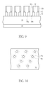
- the opening 40 a may be aligned in regular rows and columns as shown in FIG. 10 .
- Moderate space may be, but not limited, reserved between rows and columns of the openings 40 a for other opening structures to be formed therein in later process. Further detail about the opening patterns of the mask will be provided in the following embodiment.
- a brush layer 50 is formed in each opening 40 a on the mask layer 30 exposed from the dielectric layer 40 , and the opening 40 a is filled up with a self-assembled material 60 on the brush layer 50 .
- the self-assembled material 60 may include first copolymer and second copolymer mixed and bonded together by covalent bonds.
- the first copolymer and the second copolymer include different monomers, thus the two copolymers are provided with different properties.
- the first copolymer is hydrophilic and the second copolymer is hydrophobic.
- the material combination of the first copolymer and the second copolymer may include polystyrene-polymethylmethacrylate (PS-b-PMMA) copolymer, polystyrene-polymethylacrylate (PS-b-PMA) copolymer, polystyrene-polyethylmethacrylate (PS-b-PEMA) copolymer, polystyrene-polytertbutyl acrylate (PS-b-PtBA) copolymer, polystyrene-polymethylacrylate copolymer, polystyrene-poly-t-butyl methacrylate copolymer, polystyrene-polyethylacrylate copolymer, polystyrene-polyacrylate copolymer, polystyrene-polyacrylate copolymer, polystyrene-polyacrylate copolymer, polystyrene-polybutadiene
- the self-assembled material 60 may be treated by a thermal process to phase-separate the first copolymer and the second copolymer therewithin into individual regions and portions.
- the region of first copolymer and second copolymer after phase separation may be in different shapes, such as spherical, cylindrical or lamella, depending on their ratio of molar volume. For example, when the ratio of molar volume of the first copolymer to the second copolymer is about 0.2:0.8 to 0.35:0.65, the portion of first copolymer after phase separation would be in cylindrical shape, while the portion of second copolymer would filled up the space outside the portion of first copolymer.
- phase separation regions (ex. the spacing between spheres/cylinders or the total thickness of layers A, B in lamella structure) may vary with the average molecular weight of first copolymer. The larger the average molecular weight, the larger the period of phase separation regions is. In addition, the size of the phase separation regions may also vary with the average molecular weight of first copolymer. The larger the average molecular weight, the larger the size of phase separation area is.
- the brush layer 50 between the self-assembled material 60 and the mask layer 30 may be provided with the affinity identical to the first copolymer and the second copolymer.
- the so call identical affinity is that the brush layer would have same degree of surface energy with respect to the first copolymer and the second copolymer.
- the brush layer 50 may be a neutral self-assembled monolayer, which includes but not limited to phenethyltrichlorosilane (PETCS), phenyltrichlorosilane (PTCS), benzyltrichlorosilane (BZTCS), tolyltrichlorosilane (TTCS), 2-[(trimethoxysilyl)ethyl]-2-pyridine (PYRTMS), 4-biphenylyltrimeth oxysilane (BPTMS), octadecyltrichlorosilane (OTS), 1-naphthyltrimeth oxysilane (NAPTMS), 1-[(trimethoxysilyl)methyl]naphthalene (MNATMS), or (9-methylanthracenyl)trimethoxysilane (MANTMS).
- the brush layer 50 may also be constituted randomly by the first copolymer and the second copolymer. For example, the
- a phase-separating process is performed to divide the self-assembled material 60 into a first portion 60 a and a second portion 60 b, wherein the first portion 60 a is constituted by the first copolymer, such as polymethylmethacrylate (PMMA), and the second portion is constituted by the second copolymer, such as polystyrene(PS).
- the step of phase separation may include performing a thermal treatment to the self-assembled material 60 at a temperature about 150° C.-350° C.
- the second copolymer would move toward the dielectric layer 40 , thereby forming the second portion 60 b contacting the sidewall of opening 40 a, while the first copolymer move and assemble oppositely toward the center of opening and form the first portion 60 a.
- the opening 40 a is circle, and as the neutral brush layer 50 is disposed at bottom, the self-assembled material 60 formed in the opening 40 a would be cylinder, and whose first portion 60 a would also be a cylinder in the center after the phase separation.
- the second portion 60 b surrounding the first portion 60 a is between the first portion 60 a and the dielectric layer 40 .
- This kind of the phase separation may be achieved by keeping the ratio of molar volume of the first copolymer and the second copolymer within the range about 0.2:0.8 to 0.35:0.65.
- the thickness of first portion 60 a and second portion 60 b may be controlled by the molecular weights of the first copolymer and the second copolymer.
- the brush layer 50 with same surface energy is provided at bottom of the self-assembled material, the first portion 60 a and the second portion 60 b formed after the phase separation would be perfect, well-distributed cylinders perpendicular to the surface of brush layer 50 .
- the phase-separated first portion 60 a of the self-assembled material is removed from the opening to form a smaller opening 60 c therein and to expose the brush layer 50 from the opening 60 c.
- the method of removing the first portion 60 a is not particularly limited, which may include the process of oxide plasma, ozone treatment, UV treatment, pyrolysis treatment, chemical dissolution treatment, or the combination thereof, as long as the first portion 60 a may be selectively removed in the process.
- the second portion 60 b is formed inside the opening, the diameter of opening 60 c formed at this stage would be smaller than the diameter of original opening 40 a. This approach represents the dimension of the feature pattern formed by this nonconventional method is beyond the resolution limit (i.e. the diameter of original opening 40 a ) of conventional ArF photolithographic equipment.
- an etch process is performed using the remaining dielectric layer 40 and the second portion 60 b as an etch mask to remove a part of the brush layer 50 and the mask layer 30 , thereby forming a first mask pattern 30 a in the mask layer 30 . Since the underlying target layer 20 has etch selectivity with respect to the mask layer 30 , the target layer 20 would not be removed in the etch process. In this way, the mask layer would provide a portion of target pattern required for forming the semiconductor device of present invention.
- the remaining dielectric layer 40 , the brush layer 50 , and the second portion 60 b of self-assembled material are then removed by, for example, oxide plasma, ozone treatment, UV treatment, pyrolysis treatment, chemical dissolution treatment, or the combination thereof.
- the first mask pattern 30 a in the mask layer 30 at this stage is shown as the circle in FIG. 10 , wherein the first mask pattern 30 a is regularly aligned with spaces reserved between rows and columns for other openings to be formed in later process.
- only half of predetermined target pattern is formed in the present invention. The forming steps of the other half of predetermined target pattern is now described in following embodiment.
- a dielectric 42 , a brush layer 52 and a self-assembled material 62 are then formed sequentially on the mask layer 30 again, wherein the self-assembled material 62 is also divide into a first portion 62 a and a second portion 62 b by another phase-separating process.
- the manufacturing method and relevant description of above components is identical with the process flow shown in FIGS.
- FIG. 9 After the dielectric layer 42 , the brush layer 52 , and the first portion 62 a and the second portion 62 b of self-assembled material are formed, the steps of FIGS. 5-6 are repeated to remove the phase-separated first portion 62 a of self-assembled material from the openings, thereby forming a smaller opening 62 c. An etch process is then performed using the remaining dielectric layer 42 and the second portion 62 b of self-assembled material as an etch mask to form mask pattern for openings (i.e. second mask pattern 30 b ) in underlying mask layer 30 , as shown in FIG. 11 . In the view of FIG.
- the opening position of second mask pattern 30 b is defined at the space between two rows of the openings of first mask pattern 30 a, and the second mask pattern 30 b and the first mask pattern 30 a are arranged into a regular, uniform common mask pattern 30 c as shown in FIG. 12 .
- the common mask pattern 30 c is not limited to be the form as shown in FIG. 12 . Its opening pattern may also be square, rectangular or strip, and its pattern arrangement is also not limited to the form of staggered array as shown in the figure. Standard array with lower compactness may also be applied in the present invention.
- the semiconductor device mentioned in the disclosure includes the highly integrated semiconductor memory device, such as dynamic random access memory (DRAM), static random access memory (SRAM), phase change random access memory (PRAM), resistive random access memory (RRAM), magnetoresistive random access memory (MRAM), ferroelectric random access memory (FRAM), flash, micro electromechanical system (MEMS), optoelectronic device, CPU, or digital signal processing (DSP) device.
- DRAM dynamic random access memory
- SRAM static random access memory
- PRAM phase change random access memory
- RRAM resistive random access memory
- MRAM magnetoresistive random access memory
- FRAM ferroelectric random access memory
- flash micro electromechanical system
- MEMS micro electromechanical system
- optoelectronic device CPU
- DSP digital signal processing
- FIG. 13 is a schematic top view of a semiconductor memory device manufactured from the patterns formed by implementing the concept of the present invention.
- FIG. 14 is a schematic cross-sectional view of the semiconductor device taken along a section lines I-I′ and a section lines II-II′ in FIG. 13 , respectively.
- the semiconductor device includes word lines WL and bit lines BL orthogonal to word lines. The positions where the word lines and bit lines intersect are disposed with memory cell.
- a device insulating layer 101 is formed on the semiconductor substrate 100 to define active regions ACT.
- the active region ACT is a rod-shaped region with a longitudinal direction diagonal to word line WL and bit line BL.
- the word lines WL may be disposed to intersect the active regions ACT.
- the word lines WL may be formed in a recess region recessed from a surface of the semiconductor substrate 100 by predetermined depth with a gate insulating layer interposed therebetween.
- Source and drain regions 103 may be formed in the active regions ACT adjacent to opposite sides of the word lines WL.
- the source and drain regions 103 may be impurity regions doped with impurities.
- a plurality of MOS transistors may be formed on the semiconductor substrate 100 .
- the bit lines BL may be disposed on the semiconductor substrate 100 across the word lines WL.
- a first interlayer dielectric 111 may be disposed between the bit lines BL and the semiconductor substrate 100 , and bit line contact plugs BC may be formed at the first interlayer dielectric 111 to electrically connect the source and drain regions 103 to the bit line BL.
- a second interlayer dielectric 112 is formed to cover the bit lines BL.
- Contact plugs DC may be formed in the second interlayer dielectric 112 to electrically connect a data storage component to the source and drain regions 103 .
- the contact plugs DC may be disposed on the active region ACT adjacent to opposite sides of the bit line BL.
- Contact pads CP may be formed on the contact plugs DC, respectively.
- the contact pads CP may be disposed on the second interlayer dielectric 112 to increase the contact area between a bottom electrode of an overlying capacitor and the contact plugs DC.
- a mold layer 120 may be formed on a third interlayer dielectric 113 where the contact pads CP are formed. Thickness of the mold layer 120 may vary depending on height of a bottom electrode of a cylindrical capacitor.
- the mold layer 120 may include an etch-stop layer 121 , a lower mold layer 123 , a support layer 125 , and an upper mold layer 127 that are stacked in the order, wherein the lower and upper mold layers 123 and 127 may be formed of silicon oxide, and the etch-stop layer 121 and the support layer 125 may be formed of a material having an etch selectivity with respect to the lower and upper mold layers 123 and 127 during a process of dry-etching the mold layers 120 .
- the etch-stop layer 121 and the support layer 126 may be formed of silicon nitride.
- first opening 141 and the second opening 143 in FIG. 14 are formed by performing an etch process to the mold layer 120 with the mask layer 140 functions as an etch mask.
- the mask layer 14 is further formed by the above-described concept of present invention.
- the first openings 141 may be defined by using the first mask pattern 30 a and the second openings 143 may be defined by using the second mask pattern 30 b.
- the combined common mask pattern 30 c may be then used as an etch mask to form the first openings 141 and second openings 143 concurrently.
- the first openings 141 and second openings 143 may be further used to form holes 120 a in the mold layer 120 and expose the contact pads CP.
- the advantage and creativity of present invention may be achieved by using the mask patterns formed by the concept of present invention to manufacture semiconductor devices (ex. semiconductor memory devices shown in FIGS. 13 and 14 ) with larger compactness in layout unit area and uniform diameter smaller than current photolithographic resolution limit, without using expensive advanced photolithographic equipment or additional complicated processes.
Landscapes
- Engineering & Computer Science (AREA)
- Manufacturing & Machinery (AREA)
- Physics & Mathematics (AREA)
- Condensed Matter Physics & Semiconductors (AREA)
- General Physics & Mathematics (AREA)
- Computer Hardware Design (AREA)
- Microelectronics & Electronic Packaging (AREA)
- Power Engineering (AREA)
- Chemical & Material Sciences (AREA)
- Inorganic Chemistry (AREA)
- Crystallography & Structural Chemistry (AREA)
- Internal Circuitry In Semiconductor Integrated Circuit Devices (AREA)
- Semiconductor Memories (AREA)
Abstract
Description
Claims (11)
Applications Claiming Priority (3)
| Application Number | Priority Date | Filing Date | Title |
|---|---|---|---|
| CN201710066194.9A CN108400085B (en) | 2017-02-06 | 2017-02-06 | The method for forming semiconductor element pattern |
| CN201710066194.9 | 2017-02-06 | ||
| CN201710066194 | 2017-02-06 |
Publications (2)
| Publication Number | Publication Date |
|---|---|
| US20180226251A1 US20180226251A1 (en) | 2018-08-09 |
| US10157744B2 true US10157744B2 (en) | 2018-12-18 |
Family
ID=63037942
Family Applications (1)
| Application Number | Title | Priority Date | Filing Date |
|---|---|---|---|
| US15/885,827 Active US10157744B2 (en) | 2017-02-06 | 2018-02-01 | Method for forming patterns of semiconductor device |
Country Status (2)
| Country | Link |
|---|---|
| US (1) | US10157744B2 (en) |
| CN (1) | CN108400085B (en) |
Families Citing this family (3)
| Publication number | Priority date | Publication date | Assignee | Title |
|---|---|---|---|---|
| US12082401B2 (en) | 2020-11-13 | 2024-09-03 | Changxin Memory Technologies, Inc. | Semiconductor structure and formation method thereof |
| CN114496931B (en) * | 2020-11-13 | 2024-09-17 | 长鑫存储技术有限公司 | Semiconductor structure and forming method thereof |
| CN114300588B (en) * | 2021-12-30 | 2023-09-26 | 广东省科学院半导体研究所 | Method for preparing nano pattern substrate |
Citations (50)
| Publication number | Priority date | Publication date | Assignee | Title |
|---|---|---|---|---|
| US4987032A (en) * | 1987-06-26 | 1991-01-22 | Fuji Photo Film Co., Ltd. | Functional organic thin film and method of manufacture thereof |
| US6028001A (en) | 1998-04-02 | 2000-02-22 | Samsung Electronics Co., Ltd. | Methods of fabricating contact holes for integrated circuit substrates by etching to define a sidewall and concurrently forming a polymer on the sidewall |
| US6670279B1 (en) | 2002-02-05 | 2003-12-30 | Taiwan Semiconductor Manufacturing Company | Method of forming shallow trench isolation with rounded corners and divot-free by using in-situ formed spacers |
| US20040081384A1 (en) * | 2002-10-25 | 2004-04-29 | Datesman Aaron M. | Multiple-mode planar-waveguide sensor, fabrication materials and techniques |
| US6955961B1 (en) | 2004-05-27 | 2005-10-18 | Macronix International Co., Ltd. | Method for defining a minimum pitch in an integrated circuit beyond photolithographic resolution |
| US20060046261A1 (en) * | 2004-08-25 | 2006-03-02 | Sigma-Aldrich Co. | Compositions and methods employing zwitterionic detergent combinations |
| US7105431B2 (en) | 2003-08-22 | 2006-09-12 | Micron Technology, Inc. | Masking methods |
| US20060223305A1 (en) | 2005-04-04 | 2006-10-05 | Advanced Micro Devices, Inc. | Etch process for CD reduction of arc material |
| US20080171087A1 (en) * | 2006-08-16 | 2008-07-17 | Chappa Ralph A | Methods and materials for increasing the adhesion of elution control matrices to substrates |
| US20080192606A1 (en) * | 2006-10-03 | 2008-08-14 | Kabushiki Kaisha Toshiba | Magnetic recording medium, method of fabricating the same, and magnetic recording apparatus |
| US20100068783A1 (en) * | 2006-08-23 | 2010-03-18 | Isis Innovation Limited | Tailored control of surface properties by chemical modification |
| US20110259849A1 (en) * | 2010-04-27 | 2011-10-27 | Kabushiki Kaisha Toshiba | Method for producing imprint mold and magnetic recording medium |
| US20120058435A1 (en) * | 2010-09-07 | 2012-03-08 | Yuriko Seino | Pattern formation method |
| US20120164346A1 (en) * | 2010-12-22 | 2012-06-28 | Ikuo Yoneda | Method and device for forming pattern |
| US20120231213A1 (en) * | 2009-09-29 | 2012-09-13 | Kabushiki Kaisha Toshiba | Structure |
| US20120238109A1 (en) * | 2009-09-28 | 2012-09-20 | Shigeki Hattori | Method of forming pattern |
| US20120241409A1 (en) * | 2011-03-22 | 2012-09-27 | Katsutoshi Kobayashi | Pattern formation method |
| US20130323925A1 (en) * | 2012-06-04 | 2013-12-05 | Kabushiki Kaisha Toshiba | Pattern forming method, mold and data processing method |
| US8609529B2 (en) | 2012-02-01 | 2013-12-17 | United Microelectronics Corp. | Fabrication method and structure of through silicon via |
| US20140049823A1 (en) * | 2012-08-01 | 2014-02-20 | California Institute Of Technology | Birefringent polymer brush structures formed by surface initiated ring-opening metathesis polymerization |
| US20140065839A1 (en) * | 2012-09-05 | 2014-03-06 | Kabushiki Kaisha Toshiba | Method of pattern formation |
| US20140072722A1 (en) * | 2012-09-10 | 2014-03-13 | Kabushiki Kaisha Toshiba | Pattern formation method |
| US20140069325A1 (en) * | 2012-09-07 | 2014-03-13 | Kabushiki Kaisha Toshiba | Pattern forming method |
| US20140087566A1 (en) * | 2012-09-21 | 2014-03-27 | Kabushiki Kaisha Toshiba | Pattern formation method |
| US20140087291A1 (en) * | 2012-09-27 | 2014-03-27 | Kabushiki Kaisha Toshiba | Method for forming pattern and method for producing original lithography mask |
| US20140094031A1 (en) * | 2012-09-28 | 2014-04-03 | Kabushiki Kaisha Toshiba | Method for generating mask data and method for manufacturing integrated circuit device |
| US20140199847A1 (en) * | 2013-01-11 | 2014-07-17 | Kabushiki Kaisha Toshiba | Semiconductor device manufacturing method |
| US20140242799A1 (en) * | 2013-02-28 | 2014-08-28 | Kabushiki Kaisha Toshiba | Pattern formation method and method for manufacturing semiconductor device |
| US20140248439A1 (en) * | 2013-03-01 | 2014-09-04 | Kabushiki Kaisha Toshiba | Pattern formation method |
| US20140275555A1 (en) * | 2013-03-13 | 2014-09-18 | Massachusetts Institute Of Technology | Articles and methods comprising persistent carbenes and related compositions |
| US8847401B2 (en) | 2012-10-31 | 2014-09-30 | International Business Machines Corporation | Semiconductor structure incorporating a contact sidewall spacer with a self-aligned airgap and a method of forming the semiconductor structure |
| US20140295669A1 (en) * | 2013-03-27 | 2014-10-02 | Kabushiki Kaisha Toshiba | Pattern forming method |
| US20140374379A1 (en) * | 2013-06-21 | 2014-12-25 | Kabushiki Kaisha Toshiba | Pattern forming method |
| US20150151329A1 (en) * | 2013-12-02 | 2015-06-04 | Kabushiki Kaisha Toshiba | Pattern Forming Method |
| US20150195916A1 (en) * | 2012-11-21 | 2015-07-09 | International Business Machines Corporation | Formation of a composite pattern including a periodic pattern self-aligned to a prepattern |
| US20150242555A1 (en) * | 2014-02-25 | 2015-08-27 | GlobalFoundries, Inc. | Methods for fabricating integrated circuits including generating photomasks for directed self-assembly |
| US20150339429A1 (en) * | 2014-05-23 | 2015-11-26 | GlobalFoundries, Inc. | Methods for fabricating integrated circuits including generating photomasks for directed self-assembly (dsa) using dsa target patterns |
| US20160061716A1 (en) * | 2014-09-02 | 2016-03-03 | Kabushiki Kaisha Toshiba | Phase separation observation method, phase separation observation apparatus, annealing apparatus, and producing method for substrate |
| US20160064216A1 (en) * | 2014-08-29 | 2016-03-03 | Kabushiki Kaisha Toshiba | Pattern formation method |
| US20160068429A1 (en) * | 2014-09-10 | 2016-03-10 | Kabushiki Kaisha Toshiba | Pattern forming method, photomask, and template for nanoimprint |
| US20160071740A1 (en) * | 2014-09-08 | 2016-03-10 | Kabushiki Kaisha Toshiba | Pattern forming method |
| US20160068430A1 (en) * | 2014-09-10 | 2016-03-10 | Kabushiki Kaisha Toshiba | Patterning method |
| US20160077436A1 (en) * | 2014-09-11 | 2016-03-17 | Kabushiki Kaisha Toshiba | Patterning method, and template for nanoimprint and producing method thereof |
| US20160155743A1 (en) | 2014-12-02 | 2016-06-02 | Samsung Electronics Co., Ltd. | Method for Forming Patterns of Semiconductor Device |
| US20160244581A1 (en) * | 2015-02-19 | 2016-08-25 | International Business Machines Corporation | Hybrid topographical and chemical pre-patterns for directed self-assembly of block copolymers |
| US20160289248A1 (en) * | 2013-03-13 | 2016-10-06 | Massachusetts Institute Of Technology | Articles and methods comprising persistent carbenes and related compositions |
| US20170062271A1 (en) * | 2015-08-28 | 2017-03-02 | International Business Machines Corporation | Chemoepitaxy-based directed self assembly process with tone inversion for unidirectional wiring |
| US9685331B1 (en) * | 2016-02-29 | 2017-06-20 | Kabushiki Kaisha Toshiba | Semiconductor device manufacturing method and pattern forming method |
| US20170221701A1 (en) * | 2016-02-01 | 2017-08-03 | Applied Materials, Inc. | Rtp process for directed self-aligned patterns |
| US20170344691A1 (en) * | 2016-04-21 | 2017-11-30 | International Business Machines Corporation | Pattern decomposition method for wiring patterns with chemoepitaxy based directed self assembly |
Family Cites Families (4)
| Publication number | Priority date | Publication date | Assignee | Title |
|---|---|---|---|---|
| EP2839341B1 (en) * | 2012-04-16 | 2020-01-15 | Brewer Science, Inc. | Method for directed self-assembly |
| US9123541B2 (en) * | 2013-04-03 | 2015-09-01 | Brewer Science Inc. | Highly etch-resistant polymer block for use in block copolymers for directed self-assembly |
| KR102166523B1 (en) * | 2013-12-02 | 2020-10-16 | 에스케이하이닉스 주식회사 | Structure and Method of fabricating nano scale features and structure including the features |
| KR102358710B1 (en) * | 2015-04-06 | 2022-02-08 | 에스케이하이닉스 주식회사 | Method of forming different sized patterns |
-
2017
- 2017-02-06 CN CN201710066194.9A patent/CN108400085B/en active Active
-
2018
- 2018-02-01 US US15/885,827 patent/US10157744B2/en active Active
Patent Citations (50)
| Publication number | Priority date | Publication date | Assignee | Title |
|---|---|---|---|---|
| US4987032A (en) * | 1987-06-26 | 1991-01-22 | Fuji Photo Film Co., Ltd. | Functional organic thin film and method of manufacture thereof |
| US6028001A (en) | 1998-04-02 | 2000-02-22 | Samsung Electronics Co., Ltd. | Methods of fabricating contact holes for integrated circuit substrates by etching to define a sidewall and concurrently forming a polymer on the sidewall |
| US6670279B1 (en) | 2002-02-05 | 2003-12-30 | Taiwan Semiconductor Manufacturing Company | Method of forming shallow trench isolation with rounded corners and divot-free by using in-situ formed spacers |
| US20040081384A1 (en) * | 2002-10-25 | 2004-04-29 | Datesman Aaron M. | Multiple-mode planar-waveguide sensor, fabrication materials and techniques |
| US7105431B2 (en) | 2003-08-22 | 2006-09-12 | Micron Technology, Inc. | Masking methods |
| US6955961B1 (en) | 2004-05-27 | 2005-10-18 | Macronix International Co., Ltd. | Method for defining a minimum pitch in an integrated circuit beyond photolithographic resolution |
| US20060046261A1 (en) * | 2004-08-25 | 2006-03-02 | Sigma-Aldrich Co. | Compositions and methods employing zwitterionic detergent combinations |
| US20060223305A1 (en) | 2005-04-04 | 2006-10-05 | Advanced Micro Devices, Inc. | Etch process for CD reduction of arc material |
| US20080171087A1 (en) * | 2006-08-16 | 2008-07-17 | Chappa Ralph A | Methods and materials for increasing the adhesion of elution control matrices to substrates |
| US20100068783A1 (en) * | 2006-08-23 | 2010-03-18 | Isis Innovation Limited | Tailored control of surface properties by chemical modification |
| US20080192606A1 (en) * | 2006-10-03 | 2008-08-14 | Kabushiki Kaisha Toshiba | Magnetic recording medium, method of fabricating the same, and magnetic recording apparatus |
| US20120238109A1 (en) * | 2009-09-28 | 2012-09-20 | Shigeki Hattori | Method of forming pattern |
| US20120231213A1 (en) * | 2009-09-29 | 2012-09-13 | Kabushiki Kaisha Toshiba | Structure |
| US20110259849A1 (en) * | 2010-04-27 | 2011-10-27 | Kabushiki Kaisha Toshiba | Method for producing imprint mold and magnetic recording medium |
| US20120058435A1 (en) * | 2010-09-07 | 2012-03-08 | Yuriko Seino | Pattern formation method |
| US20120164346A1 (en) * | 2010-12-22 | 2012-06-28 | Ikuo Yoneda | Method and device for forming pattern |
| US20120241409A1 (en) * | 2011-03-22 | 2012-09-27 | Katsutoshi Kobayashi | Pattern formation method |
| US8609529B2 (en) | 2012-02-01 | 2013-12-17 | United Microelectronics Corp. | Fabrication method and structure of through silicon via |
| US20130323925A1 (en) * | 2012-06-04 | 2013-12-05 | Kabushiki Kaisha Toshiba | Pattern forming method, mold and data processing method |
| US20140049823A1 (en) * | 2012-08-01 | 2014-02-20 | California Institute Of Technology | Birefringent polymer brush structures formed by surface initiated ring-opening metathesis polymerization |
| US20140065839A1 (en) * | 2012-09-05 | 2014-03-06 | Kabushiki Kaisha Toshiba | Method of pattern formation |
| US20140069325A1 (en) * | 2012-09-07 | 2014-03-13 | Kabushiki Kaisha Toshiba | Pattern forming method |
| US20140072722A1 (en) * | 2012-09-10 | 2014-03-13 | Kabushiki Kaisha Toshiba | Pattern formation method |
| US20140087566A1 (en) * | 2012-09-21 | 2014-03-27 | Kabushiki Kaisha Toshiba | Pattern formation method |
| US20140087291A1 (en) * | 2012-09-27 | 2014-03-27 | Kabushiki Kaisha Toshiba | Method for forming pattern and method for producing original lithography mask |
| US20140094031A1 (en) * | 2012-09-28 | 2014-04-03 | Kabushiki Kaisha Toshiba | Method for generating mask data and method for manufacturing integrated circuit device |
| US8847401B2 (en) | 2012-10-31 | 2014-09-30 | International Business Machines Corporation | Semiconductor structure incorporating a contact sidewall spacer with a self-aligned airgap and a method of forming the semiconductor structure |
| US20150195916A1 (en) * | 2012-11-21 | 2015-07-09 | International Business Machines Corporation | Formation of a composite pattern including a periodic pattern self-aligned to a prepattern |
| US20140199847A1 (en) * | 2013-01-11 | 2014-07-17 | Kabushiki Kaisha Toshiba | Semiconductor device manufacturing method |
| US20140242799A1 (en) * | 2013-02-28 | 2014-08-28 | Kabushiki Kaisha Toshiba | Pattern formation method and method for manufacturing semiconductor device |
| US20140248439A1 (en) * | 2013-03-01 | 2014-09-04 | Kabushiki Kaisha Toshiba | Pattern formation method |
| US20140275555A1 (en) * | 2013-03-13 | 2014-09-18 | Massachusetts Institute Of Technology | Articles and methods comprising persistent carbenes and related compositions |
| US20160289248A1 (en) * | 2013-03-13 | 2016-10-06 | Massachusetts Institute Of Technology | Articles and methods comprising persistent carbenes and related compositions |
| US20140295669A1 (en) * | 2013-03-27 | 2014-10-02 | Kabushiki Kaisha Toshiba | Pattern forming method |
| US20140374379A1 (en) * | 2013-06-21 | 2014-12-25 | Kabushiki Kaisha Toshiba | Pattern forming method |
| US20150151329A1 (en) * | 2013-12-02 | 2015-06-04 | Kabushiki Kaisha Toshiba | Pattern Forming Method |
| US20150242555A1 (en) * | 2014-02-25 | 2015-08-27 | GlobalFoundries, Inc. | Methods for fabricating integrated circuits including generating photomasks for directed self-assembly |
| US20150339429A1 (en) * | 2014-05-23 | 2015-11-26 | GlobalFoundries, Inc. | Methods for fabricating integrated circuits including generating photomasks for directed self-assembly (dsa) using dsa target patterns |
| US20160064216A1 (en) * | 2014-08-29 | 2016-03-03 | Kabushiki Kaisha Toshiba | Pattern formation method |
| US20160061716A1 (en) * | 2014-09-02 | 2016-03-03 | Kabushiki Kaisha Toshiba | Phase separation observation method, phase separation observation apparatus, annealing apparatus, and producing method for substrate |
| US20160071740A1 (en) * | 2014-09-08 | 2016-03-10 | Kabushiki Kaisha Toshiba | Pattern forming method |
| US20160068430A1 (en) * | 2014-09-10 | 2016-03-10 | Kabushiki Kaisha Toshiba | Patterning method |
| US20160068429A1 (en) * | 2014-09-10 | 2016-03-10 | Kabushiki Kaisha Toshiba | Pattern forming method, photomask, and template for nanoimprint |
| US20160077436A1 (en) * | 2014-09-11 | 2016-03-17 | Kabushiki Kaisha Toshiba | Patterning method, and template for nanoimprint and producing method thereof |
| US20160155743A1 (en) | 2014-12-02 | 2016-06-02 | Samsung Electronics Co., Ltd. | Method for Forming Patterns of Semiconductor Device |
| US20160244581A1 (en) * | 2015-02-19 | 2016-08-25 | International Business Machines Corporation | Hybrid topographical and chemical pre-patterns for directed self-assembly of block copolymers |
| US20170062271A1 (en) * | 2015-08-28 | 2017-03-02 | International Business Machines Corporation | Chemoepitaxy-based directed self assembly process with tone inversion for unidirectional wiring |
| US20170221701A1 (en) * | 2016-02-01 | 2017-08-03 | Applied Materials, Inc. | Rtp process for directed self-aligned patterns |
| US9685331B1 (en) * | 2016-02-29 | 2017-06-20 | Kabushiki Kaisha Toshiba | Semiconductor device manufacturing method and pattern forming method |
| US20170344691A1 (en) * | 2016-04-21 | 2017-11-30 | International Business Machines Corporation | Pattern decomposition method for wiring patterns with chemoepitaxy based directed self assembly |
Also Published As
| Publication number | Publication date |
|---|---|
| CN108400085B (en) | 2019-11-19 |
| CN108400085A (en) | 2018-08-14 |
| US20180226251A1 (en) | 2018-08-09 |
Similar Documents
| Publication | Publication Date | Title |
|---|---|---|
| KR102270752B1 (en) | Method for forming fine patterns of semiconductor device | |
| US9087699B2 (en) | Methods of forming an array of openings in a substrate, and related methods of forming a semiconductor device structure | |
| US8999862B1 (en) | Methods of fabricating nano-scale structures and nano-scale structures fabricated thereby | |
| CN110060972B (en) | Self-aligned via and plug patterning for back end of line (BEOL) interconnects | |
| KR102190675B1 (en) | Method for forming patterns of semiconductor device | |
| US9245796B1 (en) | Methods of fabricating interconnection structures | |
| TWI550809B (en) | Directed self assembly of block copolymers to form vias aligned with interconnects | |
| US9564324B2 (en) | Methods of forming a pattern and devices formed by the same | |
| US9691614B2 (en) | Methods of forming different sized patterns | |
| US9190274B2 (en) | Methods of fabricating fine patterns | |
| US8962491B2 (en) | Methods of fabricating semiconductor devices and semiconductor devices fabricated thereby | |
| US9721795B2 (en) | Methods of forming patterns having different shapes | |
| US20180204763A1 (en) | Self-aligned isotropic etch of pre-formed vias and plugs for back end of line (beol) interconnects | |
| KR102293134B1 (en) | Method for forming fine patterns of semiconductor device | |
| US10157744B2 (en) | Method for forming patterns of semiconductor device | |
| CN106057652B (en) | Method for forming pattern | |
| US10504726B2 (en) | Nano-scale structures | |
| US20160155743A1 (en) | Method for Forming Patterns of Semiconductor Device | |
| US9478436B1 (en) | Methods for forming patterns in honeycomb array | |
| US9892918B2 (en) | Method of forming pattern of semiconductor device |
Legal Events
| Date | Code | Title | Description |
|---|---|---|---|
| FEPP | Fee payment procedure |
Free format text: ENTITY STATUS SET TO UNDISCOUNTED (ORIGINAL EVENT CODE: BIG.); ENTITY STATUS OF PATENT OWNER: LARGE ENTITY |
|
| AS | Assignment |
Owner name: UNITED MICROELECTRONICS CORP., TAIWAN Free format text: ASSIGNMENT OF ASSIGNORS INTEREST;ASSIGNORS:CHEN, KAI-PING;YU, KUEI-HSUAN;YEH, CHIU-HSIEN;AND OTHERS;REEL/FRAME:045663/0636 Effective date: 20180425 Owner name: FUJIAN JINHUA INTEGRATED CIRCUIT CO., LTD., CHINA Free format text: ASSIGNMENT OF ASSIGNORS INTEREST;ASSIGNORS:CHEN, KAI-PING;YU, KUEI-HSUAN;YEH, CHIU-HSIEN;AND OTHERS;REEL/FRAME:045663/0636 Effective date: 20180425 |
|
| STCF | Information on status: patent grant |
Free format text: PATENTED CASE |
|
| MAFP | Maintenance fee payment |
Free format text: PAYMENT OF MAINTENANCE FEE, 4TH YEAR, LARGE ENTITY (ORIGINAL EVENT CODE: M1551); ENTITY STATUS OF PATENT OWNER: LARGE ENTITY Year of fee payment: 4 |