KR20160147005A - Methods of capturing and aligning an assembly of nanowires - Google Patents
Methods of capturing and aligning an assembly of nanowires Download PDFInfo
- Publication number
- KR20160147005A KR20160147005A KR1020167033152A KR20167033152A KR20160147005A KR 20160147005 A KR20160147005 A KR 20160147005A KR 1020167033152 A KR1020167033152 A KR 1020167033152A KR 20167033152 A KR20167033152 A KR 20167033152A KR 20160147005 A KR20160147005 A KR 20160147005A
- Authority
- KR
- South Korea
- Prior art keywords
- nanowire
- nanowires
- liquid
- interface
- functionalized
- Prior art date
Links
- 239000002070 nanowire Substances 0.000 title claims abstract description 286
- 238000000034 method Methods 0.000 title claims abstract description 81
- 239000007788 liquid Substances 0.000 claims abstract description 140
- 239000000758 substrate Substances 0.000 claims abstract description 80
- 239000012071 phase Substances 0.000 claims abstract description 63
- 239000004065 semiconductor Substances 0.000 claims abstract description 15
- 239000007791 liquid phase Substances 0.000 claims abstract description 9
- 150000001875 compounds Chemical class 0.000 claims description 52
- 239000006185 dispersion Substances 0.000 claims description 46
- BGTOWKSIORTVQH-UHFFFAOYSA-N cyclopentanone Chemical compound O=C1CCCC1 BGTOWKSIORTVQH-UHFFFAOYSA-N 0.000 claims description 20
- QJAOYSPHSNGHNC-UHFFFAOYSA-N octadecane-1-thiol Chemical compound CCCCCCCCCCCCCCCCCCS QJAOYSPHSNGHNC-UHFFFAOYSA-N 0.000 claims description 14
- 230000002209 hydrophobic effect Effects 0.000 claims description 12
- 239000002105 nanoparticle Substances 0.000 claims description 11
- 239000003054 catalyst Substances 0.000 claims description 8
- 229910001218 Gallium arsenide Inorganic materials 0.000 claims description 7
- 239000007864 aqueous solution Substances 0.000 claims description 7
- 239000002245 particle Substances 0.000 claims description 7
- 229910052751 metal Inorganic materials 0.000 claims description 6
- 239000002184 metal Substances 0.000 claims description 6
- 239000000203 mixture Substances 0.000 claims description 6
- BEPFDRNIALBIKQ-UHFFFAOYSA-N 12-phosphonododecylphosphonic acid Chemical compound OP(O)(=O)CCCCCCCCCCCCP(O)(O)=O BEPFDRNIALBIKQ-UHFFFAOYSA-N 0.000 claims description 5
- 230000008859 change Effects 0.000 claims description 5
- 229920002873 Polyethylenimine Polymers 0.000 claims description 4
- HEMHJVSKTPXQMS-UHFFFAOYSA-M Sodium hydroxide Chemical compound [OH-].[Na+] HEMHJVSKTPXQMS-UHFFFAOYSA-M 0.000 description 15
- 125000000524 functional group Chemical group 0.000 description 14
- 229920000642 polymer Polymers 0.000 description 12
- XUIMIQQOPSSXEZ-UHFFFAOYSA-N Silicon Chemical compound [Si] XUIMIQQOPSSXEZ-UHFFFAOYSA-N 0.000 description 8
- 229910052710 silicon Inorganic materials 0.000 description 8
- 239000010703 silicon Substances 0.000 description 8
- LFQSCWFLJHTTHZ-UHFFFAOYSA-N Ethanol Chemical compound CCO LFQSCWFLJHTTHZ-UHFFFAOYSA-N 0.000 description 7
- 239000010931 gold Substances 0.000 description 7
- 239000010410 layer Substances 0.000 description 6
- 239000002904 solvent Substances 0.000 description 6
- -1 thiol modified gold Chemical class 0.000 description 6
- 150000001412 amines Chemical class 0.000 description 5
- 239000011521 glass Substances 0.000 description 5
- PCHJSUWPFVWCPO-UHFFFAOYSA-N gold Chemical compound [Au] PCHJSUWPFVWCPO-UHFFFAOYSA-N 0.000 description 5
- 229910052737 gold Inorganic materials 0.000 description 5
- AGBQKNBQESQNJD-UHFFFAOYSA-N lipoic acid Chemical compound OC(=O)CCCCC1CCSS1 AGBQKNBQESQNJD-UHFFFAOYSA-N 0.000 description 5
- 239000000463 material Substances 0.000 description 5
- RGSFGYAAUTVSQA-UHFFFAOYSA-N Cyclopentane Chemical compound C1CCCC1 RGSFGYAAUTVSQA-UHFFFAOYSA-N 0.000 description 4
- XYFCBTPGUUZFHI-UHFFFAOYSA-N Phosphine Chemical compound P XYFCBTPGUUZFHI-UHFFFAOYSA-N 0.000 description 4
- 150000007942 carboxylates Chemical class 0.000 description 4
- 239000002086 nanomaterial Substances 0.000 description 4
- 229910052757 nitrogen Inorganic materials 0.000 description 4
- 238000012546 transfer Methods 0.000 description 4
- RIOQSEWOXXDEQQ-UHFFFAOYSA-N triphenylphosphine Chemical compound C1=CC=CC=C1P(C=1C=CC=CC=1)C1=CC=CC=C1 RIOQSEWOXXDEQQ-UHFFFAOYSA-N 0.000 description 4
- WYTZZXDRDKSJID-UHFFFAOYSA-N (3-aminopropyl)triethoxysilane Chemical compound CCO[Si](OCC)(OCC)CCCN WYTZZXDRDKSJID-UHFFFAOYSA-N 0.000 description 3
- SDAWVOFJSUUKMR-UHFFFAOYSA-N 12-sulfanyldodecanoic acid Chemical compound OC(=O)CCCCCCCCCCCS SDAWVOFJSUUKMR-UHFFFAOYSA-N 0.000 description 3
- WEVYAHXRMPXWCK-UHFFFAOYSA-N Acetonitrile Chemical compound CC#N WEVYAHXRMPXWCK-UHFFFAOYSA-N 0.000 description 3
- YMWUJEATGCHHMB-UHFFFAOYSA-N Dichloromethane Chemical compound ClCCl YMWUJEATGCHHMB-UHFFFAOYSA-N 0.000 description 3
- 229910019142 PO4 Inorganic materials 0.000 description 3
- ABLZXFCXXLZCGV-UHFFFAOYSA-N Phosphorous acid Chemical compound OP(O)=O ABLZXFCXXLZCGV-UHFFFAOYSA-N 0.000 description 3
- YXFVVABEGXRONW-UHFFFAOYSA-N Toluene Chemical compound CC1=CC=CC=C1 YXFVVABEGXRONW-UHFFFAOYSA-N 0.000 description 3
- 239000000654 additive Substances 0.000 description 3
- 150000001298 alcohols Chemical class 0.000 description 3
- 238000000429 assembly Methods 0.000 description 3
- 230000000712 assembly Effects 0.000 description 3
- WMWFKXAWFGTUHC-UHFFFAOYSA-N butanedioic acid 2-sulfanylbutanedioic acid Chemical compound OC(=O)CCC(O)=O.OC(=O)CC(S)C(O)=O WMWFKXAWFGTUHC-UHFFFAOYSA-N 0.000 description 3
- 239000003795 chemical substances by application Substances 0.000 description 3
- 238000007306 functionalization reaction Methods 0.000 description 3
- 238000004519 manufacturing process Methods 0.000 description 3
- VLKZOEOYAKHREP-UHFFFAOYSA-N n-Hexane Chemical compound CCCCCC VLKZOEOYAKHREP-UHFFFAOYSA-N 0.000 description 3
- 235000021317 phosphate Nutrition 0.000 description 3
- 238000007711 solidification Methods 0.000 description 3
- 230000008023 solidification Effects 0.000 description 3
- 239000000243 solution Substances 0.000 description 3
- BDHFUVZGWQCTTF-UHFFFAOYSA-M sulfonate Chemical compound [O-]S(=O)=O BDHFUVZGWQCTTF-UHFFFAOYSA-M 0.000 description 3
- SYBYTAAJFKOIEJ-UHFFFAOYSA-N 3-Methylbutan-2-one Chemical compound CC(C)C(C)=O SYBYTAAJFKOIEJ-UHFFFAOYSA-N 0.000 description 2
- CSCPPACGZOOCGX-UHFFFAOYSA-N Acetone Chemical compound CC(C)=O CSCPPACGZOOCGX-UHFFFAOYSA-N 0.000 description 2
- HEDRZPFGACZZDS-UHFFFAOYSA-N Chloroform Chemical compound ClC(Cl)Cl HEDRZPFGACZZDS-UHFFFAOYSA-N 0.000 description 2
- RTZKZFJDLAIYFH-UHFFFAOYSA-N Diethyl ether Chemical compound CCOCC RTZKZFJDLAIYFH-UHFFFAOYSA-N 0.000 description 2
- BWGNESOTFCXPMA-UHFFFAOYSA-N Dihydrogen disulfide Chemical compound SS BWGNESOTFCXPMA-UHFFFAOYSA-N 0.000 description 2
- LRHPLDYGYMQRHN-UHFFFAOYSA-N N-Butanol Chemical compound CCCCO LRHPLDYGYMQRHN-UHFFFAOYSA-N 0.000 description 2
- IMNFDUFMRHMDMM-UHFFFAOYSA-N N-Heptane Chemical compound CCCCCCC IMNFDUFMRHMDMM-UHFFFAOYSA-N 0.000 description 2
- OFBQJSOFQDEBGM-UHFFFAOYSA-N Pentane Chemical compound CCCCC OFBQJSOFQDEBGM-UHFFFAOYSA-N 0.000 description 2
- BLRPTPMANUNPDV-UHFFFAOYSA-N Silane Chemical compound [SiH4] BLRPTPMANUNPDV-UHFFFAOYSA-N 0.000 description 2
- 230000001133 acceleration Effects 0.000 description 2
- 230000000996 additive effect Effects 0.000 description 2
- 150000001335 aliphatic alkanes Chemical class 0.000 description 2
- 239000011248 coating agent Substances 0.000 description 2
- 238000000576 coating method Methods 0.000 description 2
- 238000007796 conventional method Methods 0.000 description 2
- 229920001577 copolymer Polymers 0.000 description 2
- JHIVVAPYMSGYDF-UHFFFAOYSA-N cyclohexanone Chemical compound O=C1CCCCC1 JHIVVAPYMSGYDF-UHFFFAOYSA-N 0.000 description 2
- 238000000151 deposition Methods 0.000 description 2
- 230000008021 deposition Effects 0.000 description 2
- 238000000635 electron micrograph Methods 0.000 description 2
- 150000002148 esters Chemical class 0.000 description 2
- 238000002474 experimental method Methods 0.000 description 2
- DMEGYFMYUHOHGS-UHFFFAOYSA-N heptamethylene Natural products C1CCCCCC1 DMEGYFMYUHOHGS-UHFFFAOYSA-N 0.000 description 2
- ZSIAUFGUXNUGDI-UHFFFAOYSA-N hexan-1-ol Chemical compound CCCCCCO ZSIAUFGUXNUGDI-UHFFFAOYSA-N 0.000 description 2
- 238000011065 in-situ storage Methods 0.000 description 2
- 230000003993 interaction Effects 0.000 description 2
- 235000019136 lipoic acid Nutrition 0.000 description 2
- 239000000178 monomer Substances 0.000 description 2
- 239000010702 perfluoropolyether Substances 0.000 description 2
- 150000003013 phosphoric acid derivatives Chemical class 0.000 description 2
- 229910000073 phosphorus hydride Inorganic materials 0.000 description 2
- 229920000570 polyether Polymers 0.000 description 2
- 239000002243 precursor Substances 0.000 description 2
- 230000008569 process Effects 0.000 description 2
- 238000012545 processing Methods 0.000 description 2
- 230000005855 radiation Effects 0.000 description 2
- 229910000077 silane Inorganic materials 0.000 description 2
- 150000003376 silicon Chemical class 0.000 description 2
- LHUAYJZGTZYKSW-UHFFFAOYSA-M sodium;1-sulfanylpropane-1-sulfonate Chemical compound [Na+].CCC(S)S([O-])(=O)=O LHUAYJZGTZYKSW-UHFFFAOYSA-M 0.000 description 2
- 239000007787 solid Substances 0.000 description 2
- 238000001179 sorption measurement Methods 0.000 description 2
- 238000004544 sputter deposition Methods 0.000 description 2
- 150000003467 sulfuric acid derivatives Chemical class 0.000 description 2
- 229960002663 thioctic acid Drugs 0.000 description 2
- XLYOFNOQVPJJNP-UHFFFAOYSA-N water Substances O XLYOFNOQVPJJNP-UHFFFAOYSA-N 0.000 description 2
- VCUDBOXVJZSMOK-UHFFFAOYSA-N 1,1,2,2,3,3,4,4,5,5,6,6,7,7,8,8,9,9,10,10,10-henicosafluorodecane-1-thiol Chemical compound FC(F)(F)C(F)(F)C(F)(F)C(F)(F)C(F)(F)C(F)(F)C(F)(F)C(F)(F)C(F)(F)C(F)(F)S VCUDBOXVJZSMOK-UHFFFAOYSA-N 0.000 description 1
- ZRKMQKLGEQPLNS-UHFFFAOYSA-N 1-Pentanethiol Chemical compound CCCCCS ZRKMQKLGEQPLNS-UHFFFAOYSA-N 0.000 description 1
- SCOCXONJTURWMB-UHFFFAOYSA-N 11-(trimethylazaniumyl)undecane-1-thiolate;hydrobromide Chemical compound [Br-].C[N+](C)(C)CCCCCCCCCCCS SCOCXONJTURWMB-UHFFFAOYSA-N 0.000 description 1
- DZDGRVHIUYIMDS-UHFFFAOYSA-N 2-ditert-butylphosphanylethanamine Chemical compound CC(C)(C)P(C(C)(C)C)CCN DZDGRVHIUYIMDS-UHFFFAOYSA-N 0.000 description 1
- WQSCZYFOWUBINK-UHFFFAOYSA-N 5-(dithiolan-3-yl)-n-dodecylpentanamide Chemical compound CCCCCCCCCCCCNC(=O)CCCCC1CCSS1 WQSCZYFOWUBINK-UHFFFAOYSA-N 0.000 description 1
- ADLVDYMTBOSDFE-UHFFFAOYSA-N 5-chloro-6-nitroisoindole-1,3-dione Chemical compound C1=C(Cl)C([N+](=O)[O-])=CC2=C1C(=O)NC2=O ADLVDYMTBOSDFE-UHFFFAOYSA-N 0.000 description 1
- NOWKCMXCCJGMRR-UHFFFAOYSA-N Aziridine Chemical compound C1CN1 NOWKCMXCCJGMRR-UHFFFAOYSA-N 0.000 description 1
- DKPFZGUDAPQIHT-UHFFFAOYSA-N Butyl acetate Natural products CCCCOC(C)=O DKPFZGUDAPQIHT-UHFFFAOYSA-N 0.000 description 1
- OKTJSMMVPCPJKN-UHFFFAOYSA-N Carbon Chemical compound [C] OKTJSMMVPCPJKN-UHFFFAOYSA-N 0.000 description 1
- YCKRFDGAMUMZLT-UHFFFAOYSA-N Fluorine atom Chemical compound [F] YCKRFDGAMUMZLT-UHFFFAOYSA-N 0.000 description 1
- NTIZESTWPVYFNL-UHFFFAOYSA-N Methyl isobutyl ketone Chemical compound CC(C)CC(C)=O NTIZESTWPVYFNL-UHFFFAOYSA-N 0.000 description 1
- UIHCLUNTQKBZGK-UHFFFAOYSA-N Methyl isobutyl ketone Natural products CCC(C)C(C)=O UIHCLUNTQKBZGK-UHFFFAOYSA-N 0.000 description 1
- ZOKXTWBITQBERF-UHFFFAOYSA-N Molybdenum Chemical compound [Mo] ZOKXTWBITQBERF-UHFFFAOYSA-N 0.000 description 1
- 229920003171 Poly (ethylene oxide) Polymers 0.000 description 1
- DBMJMQXJHONAFJ-UHFFFAOYSA-M Sodium laurylsulphate Chemical compound [Na+].CCCCCCCCCCCCOS([O-])(=O)=O DBMJMQXJHONAFJ-UHFFFAOYSA-M 0.000 description 1
- 235000021355 Stearic acid Nutrition 0.000 description 1
- RTAQQCXQSZGOHL-UHFFFAOYSA-N Titanium Chemical compound [Ti] RTAQQCXQSZGOHL-UHFFFAOYSA-N 0.000 description 1
- 230000009471 action Effects 0.000 description 1
- 229910045601 alloy Inorganic materials 0.000 description 1
- 239000000956 alloy Substances 0.000 description 1
- 230000004075 alteration Effects 0.000 description 1
- 229920005603 alternating copolymer Polymers 0.000 description 1
- 229910052782 aluminium Inorganic materials 0.000 description 1
- 238000000137 annealing Methods 0.000 description 1
- 239000003637 basic solution Substances 0.000 description 1
- 230000015572 biosynthetic process Effects 0.000 description 1
- 229920001400 block copolymer Polymers 0.000 description 1
- 239000000872 buffer Substances 0.000 description 1
- 229910052793 cadmium Inorganic materials 0.000 description 1
- UHYPYGJEEGLRJD-UHFFFAOYSA-N cadmium(2+);selenium(2-) Chemical compound [Se-2].[Cd+2] UHYPYGJEEGLRJD-UHFFFAOYSA-N 0.000 description 1
- 229910052799 carbon Inorganic materials 0.000 description 1
- 229920006317 cationic polymer Polymers 0.000 description 1
- 239000000919 ceramic Substances 0.000 description 1
- 238000010382 chemical cross-linking Methods 0.000 description 1
- 238000006243 chemical reaction Methods 0.000 description 1
- 238000009833 condensation Methods 0.000 description 1
- 230000005494 condensation Effects 0.000 description 1
- 238000004132 cross linking Methods 0.000 description 1
- DZQISOJKASMITI-UHFFFAOYSA-N decyl-dioxido-oxo-$l^{5}-phosphane;hydron Chemical compound CCCCCCCCCCP(O)(O)=O DZQISOJKASMITI-UHFFFAOYSA-N 0.000 description 1
- 230000005684 electric field Effects 0.000 description 1
- 230000005670 electromagnetic radiation Effects 0.000 description 1
- 230000009881 electrostatic interaction Effects 0.000 description 1
- 230000008020 evaporation Effects 0.000 description 1
- 238000001704 evaporation Methods 0.000 description 1
- 239000011737 fluorine Substances 0.000 description 1
- 229910052731 fluorine Inorganic materials 0.000 description 1
- 229910052733 gallium Inorganic materials 0.000 description 1
- 238000010438 heat treatment Methods 0.000 description 1
- 125000000623 heterocyclic group Chemical group 0.000 description 1
- FUZZWVXGSFPDMH-UHFFFAOYSA-N hexanoic acid Chemical compound CCCCCC(O)=O FUZZWVXGSFPDMH-UHFFFAOYSA-N 0.000 description 1
- 229910052738 indium Inorganic materials 0.000 description 1
- MJGFBOZCAJSGQW-UHFFFAOYSA-N mercury sodium Chemical compound [Na].[Hg] MJGFBOZCAJSGQW-UHFFFAOYSA-N 0.000 description 1
- 150000002739 metals Chemical class 0.000 description 1
- HZVOZRGWRWCICA-UHFFFAOYSA-N methanediyl Chemical compound [CH2] HZVOZRGWRWCICA-UHFFFAOYSA-N 0.000 description 1
- 238000001000 micrograph Methods 0.000 description 1
- 238000012986 modification Methods 0.000 description 1
- 230000004048 modification Effects 0.000 description 1
- 229910052750 molybdenum Inorganic materials 0.000 description 1
- 239000011733 molybdenum Substances 0.000 description 1
- 239000002114 nanocomposite Substances 0.000 description 1
- 239000002073 nanorod Substances 0.000 description 1
- 239000002071 nanotube Substances 0.000 description 1
- QIQXTHQIDYTFRH-UHFFFAOYSA-N octadecanoic acid Chemical compound CCCCCCCCCCCCCCCCCC(O)=O QIQXTHQIDYTFRH-UHFFFAOYSA-N 0.000 description 1
- OQCDKBAXFALNLD-UHFFFAOYSA-N octadecanoic acid Natural products CCCCCCCC(C)CCCCCCCCC(O)=O OQCDKBAXFALNLD-UHFFFAOYSA-N 0.000 description 1
- NBIIXXVUZAFLBC-UHFFFAOYSA-K phosphate Chemical compound [O-]P([O-])([O-])=O NBIIXXVUZAFLBC-UHFFFAOYSA-K 0.000 description 1
- 239000010452 phosphate Substances 0.000 description 1
- 239000002244 precipitate Substances 0.000 description 1
- 229920005604 random copolymer Polymers 0.000 description 1
- 229910052709 silver Inorganic materials 0.000 description 1
- 239000004332 silver Substances 0.000 description 1
- 239000002356 single layer Substances 0.000 description 1
- XCTFOFPZPRZOFV-UHFFFAOYSA-M sodium;1-sulfanylethanesulfonate Chemical compound [Na+].CC(S)S([O-])(=O)=O XCTFOFPZPRZOFV-UHFFFAOYSA-M 0.000 description 1
- 238000000935 solvent evaporation Methods 0.000 description 1
- 125000006850 spacer group Chemical group 0.000 description 1
- 229920006301 statistical copolymer Polymers 0.000 description 1
- 239000008117 stearic acid Substances 0.000 description 1
- 238000003860 storage Methods 0.000 description 1
- 239000000126 substance Substances 0.000 description 1
- KDYFGRWQOYBRFD-UHFFFAOYSA-L succinate(2-) Chemical compound [O-]C(=O)CCC([O-])=O KDYFGRWQOYBRFD-UHFFFAOYSA-L 0.000 description 1
- 229910052717 sulfur Inorganic materials 0.000 description 1
- 238000004381 surface treatment Methods 0.000 description 1
- 229910052714 tellurium Inorganic materials 0.000 description 1
- ZGNPLWZYVAFUNZ-UHFFFAOYSA-N tert-butylphosphane Chemical compound CC(C)(C)P ZGNPLWZYVAFUNZ-UHFFFAOYSA-N 0.000 description 1
- 150000003573 thiols Chemical class 0.000 description 1
- 239000010936 titanium Substances 0.000 description 1
- 229910052719 titanium Inorganic materials 0.000 description 1
- 238000013518 transcription Methods 0.000 description 1
- 230000035897 transcription Effects 0.000 description 1
- BNCXNUWGWUZTCN-UHFFFAOYSA-N trichloro(dodecyl)silane Chemical compound CCCCCCCCCCCC[Si](Cl)(Cl)Cl BNCXNUWGWUZTCN-UHFFFAOYSA-N 0.000 description 1
- 238000009736 wetting Methods 0.000 description 1
- 229910052725 zinc Inorganic materials 0.000 description 1
Images


Classifications
-
- H01L29/0676—
-
- B—PERFORMING OPERATIONS; TRANSPORTING
- B05—SPRAYING OR ATOMISING IN GENERAL; APPLYING FLUENT MATERIALS TO SURFACES, IN GENERAL
- B05D—PROCESSES FOR APPLYING FLUENT MATERIALS TO SURFACES, IN GENERAL
- B05D1/00—Processes for applying liquids or other fluent materials
- B05D1/18—Processes for applying liquids or other fluent materials performed by dipping
- B05D1/20—Processes for applying liquids or other fluent materials performed by dipping substances to be applied floating on a fluid
- B05D1/202—Langmuir Blodgett films (LB films)
-
- H01L29/20—
-
- H01L29/22—
-
- H01L31/035227—
-
- H01L31/1828—
-
- H01L31/184—
-
- B—PERFORMING OPERATIONS; TRANSPORTING
- B82—NANOTECHNOLOGY
- B82Y—SPECIFIC USES OR APPLICATIONS OF NANOSTRUCTURES; MEASUREMENT OR ANALYSIS OF NANOSTRUCTURES; MANUFACTURE OR TREATMENT OF NANOSTRUCTURES
- B82Y10/00—Nanotechnology for information processing, storage or transmission, e.g. quantum computing or single electron logic
-
- B—PERFORMING OPERATIONS; TRANSPORTING
- B82—NANOTECHNOLOGY
- B82Y—SPECIFIC USES OR APPLICATIONS OF NANOSTRUCTURES; MEASUREMENT OR ANALYSIS OF NANOSTRUCTURES; MANUFACTURE OR TREATMENT OF NANOSTRUCTURES
- B82Y15/00—Nanotechnology for interacting, sensing or actuating, e.g. quantum dots as markers in protein assays or molecular motors
-
- B—PERFORMING OPERATIONS; TRANSPORTING
- B82—NANOTECHNOLOGY
- B82Y—SPECIFIC USES OR APPLICATIONS OF NANOSTRUCTURES; MEASUREMENT OR ANALYSIS OF NANOSTRUCTURES; MANUFACTURE OR TREATMENT OF NANOSTRUCTURES
- B82Y40/00—Manufacture or treatment of nanostructures
-
- Y—GENERAL TAGGING OF NEW TECHNOLOGICAL DEVELOPMENTS; GENERAL TAGGING OF CROSS-SECTIONAL TECHNOLOGIES SPANNING OVER SEVERAL SECTIONS OF THE IPC; TECHNICAL SUBJECTS COVERED BY FORMER USPC CROSS-REFERENCE ART COLLECTIONS [XRACs] AND DIGESTS
- Y02—TECHNOLOGIES OR APPLICATIONS FOR MITIGATION OR ADAPTATION AGAINST CLIMATE CHANGE
- Y02E—REDUCTION OF GREENHOUSE GAS [GHG] EMISSIONS, RELATED TO ENERGY GENERATION, TRANSMISSION OR DISTRIBUTION
- Y02E10/00—Energy generation through renewable energy sources
- Y02E10/50—Photovoltaic [PV] energy
- Y02E10/544—Solar cells from Group III-V materials
-
- Y—GENERAL TAGGING OF NEW TECHNOLOGICAL DEVELOPMENTS; GENERAL TAGGING OF CROSS-SECTIONAL TECHNOLOGIES SPANNING OVER SEVERAL SECTIONS OF THE IPC; TECHNICAL SUBJECTS COVERED BY FORMER USPC CROSS-REFERENCE ART COLLECTIONS [XRACs] AND DIGESTS
- Y02—TECHNOLOGIES OR APPLICATIONS FOR MITIGATION OR ADAPTATION AGAINST CLIMATE CHANGE
- Y02P—CLIMATE CHANGE MITIGATION TECHNOLOGIES IN THE PRODUCTION OR PROCESSING OF GOODS
- Y02P70/00—Climate change mitigation technologies in the production process for final industrial or consumer products
- Y02P70/50—Manufacturing or production processes characterised by the final manufactured product
Landscapes
- Engineering & Computer Science (AREA)
- Nanotechnology (AREA)
- Chemical & Material Sciences (AREA)
- Crystallography & Structural Chemistry (AREA)
- Physics & Mathematics (AREA)
- Materials Engineering (AREA)
- Health & Medical Sciences (AREA)
- Molecular Biology (AREA)
- General Health & Medical Sciences (AREA)
- Life Sciences & Earth Sciences (AREA)
- Condensed Matter Physics & Semiconductors (AREA)
- General Physics & Mathematics (AREA)
- Manufacturing & Machinery (AREA)
- Mathematical Physics (AREA)
- Theoretical Computer Science (AREA)
- Photovoltaic Devices (AREA)
- Silicon Compounds (AREA)
- Pharmaceuticals Containing Other Organic And Inorganic Compounds (AREA)
Abstract
본 실시예는 배향된 나노와이어 조립체를 액체 계면에서 표면으로 전사하는 방법으로서, 상기 방법은 제1액체 및 제2액체를 제공하고, 제1 및 제2액체 상은 하부 상, 상부 상, 하부 상과 상부 상 사이의 계면으로 분리되며; 대부분의 나노와이어가 계면에 위치하도록 제1 및 제2액체에서 반도체 나노와이어를 포함하는 나노와이어를 제공하며; 기판상에서 다수의 나노와이어가 서로에 대해 정렬되도록 기판에 나노와이어를 제공하는 것을 포함하는 것을 특징으로 하는 방법이다.This embodiment provides a method for transferring an oriented nanowire assembly from a liquid interface to a surface, the method comprising providing a first liquid and a second liquid, wherein the first and second liquid phases comprise a lower phase, Separated at the interface between the upper and upper phases; Providing a nanowire comprising semiconductor nanowires in the first and second liquids such that the majority of the nanowires are at the interface; And providing nanowires to the substrate such that the plurality of nanowires are aligned with respect to one another on the substrate.
Description
본 출원은 2014년 4월 29일 출원된 스위치 특허 출원 제1430057-8호와 관련되고, 그 전체 내용은 참조로 본 명세서에 통합된다. The present application is related to Switch Patent Application No. 1430057-8 filed on April 29, 2014, the entire contents of which are incorporated herein by reference.
본 발명은 나노와이어 장치의 형성, 특히 나노와이어 장치를 만들기 위한 나노와이어의 캡처 및 정렬에 관한 것이다.The present invention relates to the formation of nanowire devices, and in particular to the capture and alignment of nanowires for making nanowire devices.
표면에 나노 구조를 캡처하는 기존의 기술은, 낮은 길이-직경비(예를 들면, 나노 로드, 나노 입자)를 갖는 나노 구조의 정렬 및 캡처/증착에 포커스를 맞추고 있다. 그러나, 상당한 길이-직경비(예를 들면, 나노와이어)를 갖는 나노 구조의 캡처와 정렬은 더 어렵다. 나노와이어를 선호하는 방향으로 정렬하는 것 역시 어렵다. 기존의 기술은 나노 구조들의 정렬과 캡처/증착을 달성하기 위해 외부 장비 또는 고전압의 사용을 요구할 수 있는 외부 제어(예를 들면, 인가된 전계, 느린 용매 증발 또는 고온 어닐링)를 사용한다. 외부 제어는 생산 비용을 증가시키고 나노와이어 장치 생산의 확장성(scalabilty)을 감소시킨다. Conventional techniques for capturing nanostructures on the surface focus on alignment and capture / deposition of nanostructures with low length-to-diameter ratios (e.g., nanorods, nanoparticles). However, the capture and alignment of nanostructures with considerable length-to-diameter ratios (e.g., nanowires) is more difficult. It is also difficult to align the nanowires in the preferred orientation. Conventional techniques use external equipment (e.g., an applied electric field, slow solvent evaporation, or high temperature annealing) that may require the use of external equipment or high voltage to achieve alignment and capture / deposition of nanostructures. External control increases production costs and reduces the scalability of nanowire device production.
본 발명은 나노와이어 조립체의 캡처 및 정렬 방법을 제공하는 것을 목적으로 한다. The present invention seeks to provide a method of capturing and aligning nanowire assemblies.
실시예는 배향된 나노와이어의 조립체를 액체 계면으로부터 제1액체 및 제2액체의 제공을 포함하는 표면으로 전사하는 방법에 관한 것이다. 제1 및 제2액체는 하부 상, 상부 상 및 하부 상과 상부 상 사이의 계면으로 분리된다. 또한, 상기 방법은 제1 및 제2액체에 나노와이어를 제공하여 대부분의 나노와이어가 계면에 위치하도록 하여 기판에 나노와이어를 제공하여 다수의 나노와이어가 기판에서 서로에 대해 정렬되도록 한다.An embodiment is directed to a method of transferring an assembly of oriented nanowires from a liquid interface to a surface comprising providing a first liquid and a second liquid. The first and second liquids are separated into a lower phase, an upper phase and an interface between the lower phase and the upper phase. The method also provides nanowires in the first and second liquids so that most of the nanowires are at the interface, thereby providing the nanowires on the substrate such that the plurality of nanowires are aligned with respect to each other on the substrate.
본 발명은 나노와이어 조립체의 캡처 및 정렬 방법을 제공한다.The present invention provides a method for capturing and aligning nanowire assemblies.
도 1은 본 발명의 실시예에 따른 나노와이어 조립체의 캡처 및 조립 방법을 개략적으로 도시한 도면이다.
도 2는 본 발명의 실시예에 따른 기능화된 나노와이어를 개략적으로 도시한 도면이다.
도 3은 본 발명의 실시예에 따른 정렬 및 조립된 나노와이어의 방법을 개략적으로 도시한 도면이다.
도 4는 본 발명의 실시예에 따른 나노와이어 조립체를 캡처 및 정렬하는 방법을 개략적으로 도시한 도면이다.
도 5는 본 발명의 원리에 따른 실시예의 솔라 셀(solar cell)의 측면도이다.
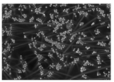
도 6-10은 본 발명의 실시예에 따른 정렬된 나노와이어 조립체의 전자 현미경(SEM) 사진이다.1 is a schematic view illustrating a method of capturing and assembling a nanowire assembly according to an embodiment of the present invention.
Figure 2 is a schematic illustration of a functionalized nanowire according to an embodiment of the present invention.
Figure 3 is a schematic illustration of a method of aligned and assembled nanowires according to embodiments of the present invention.
4 is a schematic illustration of a method for capturing and aligning a nanowire assembly in accordance with an embodiment of the present invention.
5 is a side view of a solar cell of an embodiment according to the principles of the present invention.
6-10 are electron micrograph (SEM) photographs of an aligned nanowire assembly according to an embodiment of the present invention.
방법의 실시예는 용기에 위치한 제1액체와 제1액체에 첨가된 나노와이어 분산액을 사용한다. 나노와이어 분산액은 분산액 내에서 사전-조립된 나노와이어를 분산시킴으로써 제조된다. 즉, 분산액 내의 인-시투(in-situ) 형성 나노와이어와 대조적으로 나노와이어는 분산액에 첨가되기 이전에 조립된다. 본 실시예에서, 분산액이 선택되어 나노와이어 분산액이 제1액체에서 비혼화성이거나 부분적으로 혼화성이 된다. 이러한 방식으로, 나노와이어 분산액이 제1액체에 첨가될 때, 제1액체와 분산액의 상이 분리되고, 두 개의 액상 시스템을 만든다. 더 밀도가 높은 액체는 용기의 바닥에 침전하며 하부 상을 형성하고, 반면 밀도가 더 낮은 액체는 제1액체의 상부에 뜨며 상부 상을 형성한다. 그 결과 생성된 2상 시스템은 상부 상과 하부 상, 그리고 상부 상과 하부 상 사이의 계면을 갖는다.An embodiment of the method uses a first liquid located in the vessel and a nanowire dispersion added to the first liquid. Nanowire dispersions are prepared by dispersing pre-assembled nanowires in a dispersion. That is, in contrast to the in-situ forming nanowires in the dispersion, the nanowires are assembled before being added to the dispersion. In this embodiment, the dispersion is selected such that the nanowire dispersion is incompatible or partially miscible in the first liquid. In this manner, when the nanowire dispersion is added to the first liquid, the phase of the first liquid and the dispersion is separated and produces two liquid phase systems. The more dense liquid precipitates at the bottom of the vessel and forms the lower phase, while the less dense liquid floats on top of the first liquid to form the upper phase. The resulting two-phase system has an interface between the upper and lower phases, and between the upper and lower phases.
본 발명의 일 실시예에서, 나노와이어 분산액 내 나노와이어는 같은 물질로 구성될 수 있다. 또는, 나노와이어 분산액은 다른 물질로 구성된 나노와이어를 포함할 것이다. 본 실시예 및 아래의 실시예에서 사용이 적합한 나노와이어 물질은 금속(예를 들면, 금, 은과 그 합금), 카본 나노와이어 또는 나노 튜브(단일층 또는 복합층), III-V(GaAs 및 InP와 같은 Al, In, Ga, N, P, As로 구성된 이원, 삼원, 사원 III-V 반도체 포함)을 포함한 반도체 및 II-VI 반도체(ZnO, CdSe와 같은 Zn, Cd, Se, O, S, Te로 구성된 이원, 삼원, 사원 II-V 반도체 포함), 세라믹을 포함한다. 나노와이어는 수용된 상태로 사용되거나 하나 이상의 표면 처리를 받을 수 있을 것이다.In one embodiment of the invention, the nanowires in the nanowire dispersion can be composed of the same material. Alternatively, the nanowire dispersion will comprise nanowires made of different materials. Suitable nanowire materials for use in this and the following examples include metals (e.g., gold, silver and alloys thereof), carbon nanowires or nanotubes (single or multiple layers), III-V VI and III-VI semiconductors (Zn, Cd, Se, O, S), such as ZnO and CdSe, including semiconductors and III-V semiconductors including Al, In, Ga, N, , Te, Bi-Si, and II-V semiconductors), ceramics. The nanowires may be used as received or may be subjected to one or more surface treatments.
제1액체에 나노와이어 분산액을 첨가한 후, 대부분의 나노와이어는 계면에서 조립된다. 일반적으로, 나노와이어는 계면에서 자발적으로 조립되는데, 즉, 나노와이어는 충분한 시간이 주어지면, 계면에서 자기 정렬한다. 그러나, 나노와이어는 그 계면에서 나노와이어의 조립을 촉진 또는 가속하는 하나 이상의 조건들에 적용되기 쉽다. 가속은 몇 가지 방법으로 이루어질 수 있다. 예를 들면, 가속은 상부 상의 조성물, 하부 상의 조성물의 변경 또는 용기의 온도의 변경을 통해 이루어질 수 있다. After adding the nanowire dispersion to the first liquid, most of the nanowires are assembled at the interface. Generally, the nanowires are spontaneously assembled at the interface, that is, the nanowires self-align at the interface given sufficient time. However, the nanowire is susceptible to one or more conditions that promote or accelerate the assembly of the nanowire at the interface. Acceleration can be achieved in several ways. For example, the acceleration may be through composition on the top, change of composition on the bottom, or alteration of the temperature of the container.
본 발명의 일 실시예에서, 2상 시스템의 상부 상은 2상 시스템의 상부 상의 나노와이어의 길이보다 더 두껍다(예를 들면, 도 2-4에 도시된 바와 같이, 상부 상은 나노와이어의 길이보다 큰 값인 H2의 높이를 갖는다). 선택적으로, 상부 상은 나노와이어를 기판으로 전사하기 전 용기에서 부분적으로 또는 완전히 제거될 수 있다.In one embodiment of the invention, the top image of the two-phase system is thicker than the length of the nanowire on top of the two-phase system (e.g., as shown in Figures 2-4, Value H2). Optionally, the top phase may be partially or completely removed from the vessel prior to transferring the nanowires to the substrate.
정렬된 나노와이어 조립체를 형성한 후에, 정렬된 나노와이어는 용기에서 기판으로 전사될 수 있다. 본 발명의 일 실시예에서, 기판의 표면은 기능화(functionalized)된다. 기능화 화합물은 나노와이어를 기판 표면에 붙드는(securing) 것을 돕는다. 본 발명의 일 실시예에서, 계면을 교차하는 기판의 기능화된 표면을 이동하여 계면에서 기능화된 표면을 나노와이어에 접촉하도록 움직임으로써 이루어진다. 기판은 액체 계면에 대하여 수직, 수평 또는 일정 각도로 기울게 배향될 수 있다. After forming the aligned nanowire assembly, the aligned nanowires can be transferred from the container to the substrate. In one embodiment of the invention, the surface of the substrate is functionalized. The functionalized compound helps to secure the nanowire to the substrate surface. In one embodiment of the invention, the functionalized surface of the substrate crossing the interface is moved to move the functionalized surface at the interface to contact the nanowire. The substrate may be oriented perpendicularly, horizontally, or at an angle to the liquid interface.
특정한 작용기를 포함하는 기능 종의 화학 반응 또는 물리적 흡착에 의해 기판의 표면이 변형될 수 있다(예를 들면, 기능화됨). 또는, 기판 표면이 수용된 상태로 사용될 수 있다(즉, 베어(bare)). 이것들로 한정되는 것은 아니지만, 사용될 수 있는 기판의 예로, 실리콘, 몰리브덴, 실란 변성 실리콘, 금, 티올 변형 금 또는 물리적으로 흡착된 양이온 성 중합체를 갖는 실리콘 표면을 포함한다.The surface of the substrate may be deformed (e. G., Functionalized) by chemical reaction or physical adsorption of a functional species comprising a particular functional group. Alternatively, the substrate surface may be used as received (i.e., bare). Examples of substrates that may be used include, but are not limited to, silicon, molybdenum, silane-modified silicon, gold, thiol modified gold, or a silicon surface having a physically adsorbed cationic polymer.
또 다른 실시예에서, 나노와이어 분산액을 제1액체에 첨가하는 것보다 먼저, 2상 액체 시스템을 형성한 다음 나노와이어를 시스템에 첨가한다. 따라서, 제1액체와 다른 제2액체는 제1액체에 첨가될 수 있다. 바람직하게는, 제2액체는 제1액체에 대해 비혼화성이거나 부분적 혼화성/부분적 비혼화성이다. 이러한 방식으로 그리고 이전의 실시예와 유사하게, 제2액체가 제1액체에 첨가되면, 두 액체의 상은 분리되고, 2상 액체 시스템을 만든다. 밀도가 높은 액체는 용기의 바닥에 침전하고, 반면 밀도가 낮은 액체는 제1액체의 상부에 뜨며, 그 결과 상부 상과 하부 상, 그리고 상부와 하부 상 사이의 계면으로 구성되는 2상 시스템을 초래한다. 본 발명의 일 실시예에서, 나노와이어 또는 나노와이어 분산액은 제2액체를 제1액체에 첨가하기 전 2상 시스템에 첨가되거나 제1액체에 첨가될 수 있다. 나노와이어 분산액은 분산액에 분산된 나노와이어(예를 들면, 용매)로 구성된다. 분산액은 제1액체 또는 제2액체와 같다. 또는, 분산액은 제1 및 제2액체 모두와 다른 제3액체일 것이다. 또는 건조 나노와이어가 첨가될 수 있다.In another embodiment, prior to adding the nanowire dispersion to the first liquid, a two-phase liquid system is formed and nanowires are added to the system. Thus, a second liquid different from the first liquid may be added to the first liquid. Preferably, the second liquid is incompatible or partially miscible / partially incompatible with the first liquid. In this manner and similar to the previous embodiment, when a second liquid is added to the first liquid, the phases of the two liquids are separated and produce a two-phase liquid system. Higher density liquids settle on the bottom of the vessel, while less dense liquid floats on top of the first liquid, resulting in a two-phase system consisting of the upper and lower phases, and the interface between the upper and lower phases do. In one embodiment of the invention, the nanowire or nanowire dispersion may be added to the two-phase system or added to the first liquid prior to adding the second liquid to the first liquid. The nanowire dispersion is composed of nanowires (e.g., a solvent) dispersed in a dispersion. The dispersion liquid is the same as the first liquid or the second liquid. Alternatively, the dispersion will be a third liquid different from both the first and second liquids. Or dry nanowires may be added.
기능화 화합물과 액체들의 종류 및 조성(예를 들면, 제1액체, 분산액, 제2액체 및 첨가제(사용되는 경우))의 선택에 기반하여, 나노와이어의 방향과 정렬이 제어될 수 있다. 이와 유사한 방법으로, 이 변수/조성 변수가 나노와이어-나노와이어 사이 간격을 서로 다르게 하는 것을 허용할 것이며, 그 결과 서로 다른 (즉, 미리 선택된) 밀도(예를 들면, 평방 미크론 당 나노와이어들의 밀도)를 가진 조립체를 초래한다. 나노와이어-나노와이어 사이 간격은, 기판에서 정렬된 나노와이어의 캡처 후, 덮인 표면적의 퍼센티지로부터 추론될 수 있다.The orientation and alignment of the nanowires can be controlled, based on the selection of the type and composition of the functionalized compound and liquids (e.g., the first liquid, the dispersion, the second liquid, and the additive, if used). In a similar manner, this variable / composition variable will allow different spacing between nanowires and nanowires, resulting in different (i.e., preselected) densities (e.g., density of nanowires per square micron ). ≪ / RTI > The spacing between the nanowires-nanowires can be deduced from the percentage of the surface area covered after capturing the aligned nanowires at the substrate.
본 발명의 일 실시예에서, 방법은 나노와이어 조립체를 고정하는 추가적인 단계를 포함한다. 본 실시예에서, 고화제가 액체의 상부 상과 하부 상의 고화를 야기하는 나노와이어 조립체와 함께 용기에 첨가된다. 본 발명의 일 실시예에서, 고화된 상은 부드러운 층(예를 들면, 겔 또는 유연한 고체 층)으로, 나노와이어를 붙든다. 또는, 만약 상부 액체 상이 완전히 제거된다면, 액체가 첨가될 것이고, 액체의 하부 상이 고화되어 나노와이어 조립체를 붙들도록 초래할 것이다. 또 다른 실시예에서, 액체 중 하나가 상부 또는 하부 상을 고화하기 위해 방사선(예를 들면, 가시 광선 또는 자외선과 같은 열 또는 전자기 방사선)에 노출될 수 있다. 또 다른 실시예에서, 제1액체, 분산액 또는 제2액체는 시간을 통해 스스로 고화하는 액체다. 이러한 방법으로, 나노와이어는 상부(또는 하부)상에서 고정될 수 있다. 또 다른 실시예에서, 만약 상부 액체 상이 상당히 제거되면, 하부 액체 상과 접촉하게 될 때 액체가 첨가되고, 고화하고, 나노조립체를 붙들 것이다.In one embodiment of the invention, the method comprises an additional step of securing the nanowire assembly. In this embodiment, a solidifying agent is added to the vessel along with a nanowire assembly that causes solidification on the top and bottom of the liquid. In one embodiment of the present invention, the solidified phase holds the nanowire with a soft layer (e.g., a gel or a flexible solid layer). Alternatively, if the upper liquid phase is completely removed, liquid will be added, causing the lower phase of liquid to solidify and hold the nanowire assembly. In another embodiment, one of the liquids may be exposed to radiation (e.g., heat or electromagnetic radiation, such as visible light or ultraviolet radiation) to solidify the upper or lower image. In yet another embodiment, the first liquid, dispersion or second liquid is a liquid that solidifies itself over time. In this way, the nanowire can be fixed on the top (or bottom). In another embodiment, if the upper liquid phase is significantly removed, the liquid will be added, solidified, and will hold the nanocomposite when it comes into contact with the lower liquid phase.
본 발명의 일 실시예에서, 계면에서 정렬된 나노와이어와 접촉하는 기능화된 기판의 표면을 포지셔닝함으로써, 상부 상과 하부 상 사이 계면에 정렬된, 바람직하게는 나노와이어의 장축이 계면의 표면과 실질적으로 수직하게 정렬된, 나노와이어는 기능화된 기판으로 정렬된 채로 전사된다. 나노와이어의 조립체는 정렬된 나노와이어와 기능화된 표면의 정전기 상호 작용의 결과 또는 나노와이어와 기능화된 표면의 반데어 발트(van der Waals) 상호작용의 결과로 계면에서 기능화된 기판의 표면으로 전사된다.In one embodiment of the present invention, by positioning the surface of the functionalized substrate in contact with the aligned nanowires at the interface, the long axis of the nanowire, preferably aligned at the interface between the upper and lower phases, The nanowires are transferred while being aligned with the functionalized substrate. The assembly of nanowires is transferred from the interface to the surface of the functionalized substrate as a result of electrostatic interaction of the aligned nanowires and the functionalized surface or van der Waals interaction of the nanowire with the functionalized surface .
기능화 화합물 선택 시 고려되어야 할 변수는 나노와이어 전사/캡처 단계에서 기능화된 표면의 습윤성이다. 기판의 표면은 제1액체에 적절히 젖어야 한다. 즉, 기능화된 기판 표면에서 나노와이어 조립체의 전사가 자발적이고(즉, 보조 없이), 빠른 속도로 발생할 수 있도록 해야 한다. 본 발명의 일 실시예에서, 제1액체는 기능화된 표면에서 약 130도보다 적은 접촉 각을 가질 것이다. 바람직하게는, 접촉 각은 0 에서 75°와 같이, 90도보다 적다. 바람직하게는, 기능화된 기판 표면의 젖음은 나노와이어 조립체의 출현에 의해 촉진된다. 특정 캡처 형상에서는, 제1 및/또는 제2액체와 기능화된 표면의 고접촉각(예를 들어, >90°)이 바람직하다. 특히, 기능화된 표면이 나노와이어 조립체와 접촉하도록 허용되고 기능화된 표면이 실질적으로 액체의 계면에 수평인 경우. 이러한 상황에서는, 기능화된 표면은 액체 계면을 절대 실제로 교차하지 않고, 대신 단순히 액체의 계면의 한 측면으로부터 나노와이어 조립체를 집어 낸다. The parameter to be considered when selecting the functionalized compound is the wettability of the functionalized surface in the nanowire transcription / capture step. The surface of the substrate must be properly wetted with the first liquid. That is, the transfer of the nanowire assembly from the functionalized substrate surface must occur spontaneously (i.e., without assistance) and at a rapid rate. In one embodiment of the present invention, the first liquid will have a contact angle less than about 130 degrees at the functionalized surface. Preferably, the contact angle is less than 90 degrees, such as 0 to 75 degrees. Preferably, the wetting of the functionalized substrate surface is facilitated by the appearance of the nanowire assembly. In certain capture geometries, a high contact angle (e.g., > 90 DEG) of the first and / or second liquid and the functionalized surface is preferred. In particular, when the functionalized surface is allowed to contact the nanowire assembly and the functionalized surface is substantially horizontal to the interface of the liquid. In such a situation, the functionalized surface never actually intersects the liquid interface, but instead simply picks up the nanowire assembly from one side of the interface of the liquid.
본 발명의 일 실시예에서, 나노와이어는 나노와이어가 소수성(펜타티올(Pentanethiol), 퍼플루오로데칸티올(perfluorodecane thiol), 도데실트리클로로실란(dodecyltrichlorosilane), 스테아르산(stearic acid), 데실포스폰산(decyl phosphonic acid), 5-(1,2-디티올란-3-일)-N-도데실펜탄아미드(5-(1,2-dithiolan-3-yl)-N-dodecylpentanamide), 나트륨 도데실설페이트(sodium dodecyl sulfate), 트리페닐포스핀, 옥타데실티올(triphenyl phosphine, octadecylthiol)과 같은) 알칸, 불소제 포함) 및/또는 친수성(나트륨 메르캅토프로판 술포네이트(sodium mercaptopropane sulfonate), 나트륨 메르캅토에탄술포네이트(sodium mercaptoethane sulfonate), 메르캅토알칸 석시네이트(2-메르캅토석시네이트)(mercaptoalkane succinate(2-mercaptosuccinate)), 메르캅토알칸 아민(mercaptoalkane amine), (11-메르캅토운데실)-N, N, N-트리메틸암모늄브로마이드((11-mercaptoundecyl)-N,N,N-trimethylammonium bromide), (12-포스포노도데실)포스폰산((12-Phosphonododecyl)phosphonic acid, (±) -1,2-디티올란-3-펜탄산(리포산으로도 공지됨)((±)-1,2-Dithiolane-3-pentanoic acid), (2-암모니에틸)디-테르트-부틸포스포늄비스(테트라플루오로보레이트)((2-Ammonioethyl)di-tert-butylphosphonium bis(tetrafluoroborate)), (3-아미노프로필)트리에톡시실란((3-Aminopropyl)triethoxysilane), 12-메르캅토도데카노인산(12-mercaptododecanoic acid)과 같은) 황산염, 인산염, 카르복실산염, 아민, 폴리에테르 포함)을 부여하는 화합물로 기능화될 수 있다. 본 발명의 일 실시예에서, 액체 계면에서 수직 정렬을 달성하기 위해 서로 다른 기능화 화합물을 사용하여 나노와이어 표면의 한 부분에 소수성이 부여되고 나노와이어 표면의 나머지 부분은 친수성이 부여된다. 또 다른 실시예에서, 나노와이어 표면의 오직 한 부분만 기능화 화합물로 다루어진다.In one embodiment of the invention, the nanowire is a nanowire wherein the nanowire is hydrophobic (such as pentanethiol, perfluorodecane thiol, dodecyltrichlorosilane, stearic acid, Decyl phosphonic acid, 5- (1,2-dithiolan-3-yl) -N-dodecylpentanamide, 5- (Such as sodium dodecyl sulfate, triphenyl phosphine, triphenyl phosphine, octadecylthiol) alkanes and fluorine agents) and / or hydrophilic (such as sodium mercaptopropane sulfonate, sodium mercury, Mercaptoalkane succinate (2-mercaptosuccinate), mercaptoalkane amine, (11-mercaptoundecyl (2-mercaptosuccinate)), mercaptoalkane sulfonate, mercaptoalkane succinate ) -N, N, N-trimethylammonium bromide ((11-mercaptoundec N, N-trimethylammonium bromide, (12-Phosphonododecyl) phosphonic acid, (±) -1,2-dithiolan-3-pentanoic acid (2-Ammonioethyl) di-tert-butylphosphonium bis (tetrafluoroborate) (also known as (±) -1,2-Dithiolane-3-pentanoic acid, sulfates such as tert-butylphosphonium bis (tetrafluoroborate), (3-aminopropyl) triethoxysilane, 12-mercaptododecanoic acid), phosphates, Amines, polyethers, etc.) in the presence of a catalyst. In one embodiment of the present invention, hydrophobic properties are imparted to one portion of the nanowire surface and hydrophilicity is imparted to the rest of the nanowire surface using different functional compounds to achieve vertical alignment at the liquid interface. In yet another embodiment, only a portion of the nanowire surface is treated as a functional compound.
도 1은 본 발명의 실시예에 따른 나노와이어 조립체의 캡처 및 정렬 방법을 개략적으로 도시한 도면이다. 본 실시예의 제1단계1에서, 제1액체는 하부 상(102)을 형성하기 위해 용기(100)에 담긴다. 비커, 자(jar), 배럴(barrel) 등과 같이 액체를 담을 수 있는 모든 용기(100)가 사용될 수 있다. 본 발명의 일 실시예에서, 제1액체는 NaOH 용액 또는 다른 염기성 용액 같은 염기성 수용액(pH 7 이상)이다. 용액의 pH는, 예를 들면 10-12와 같이, 9-13의 범위 내에 있을 것이다. 선택적으로, 하나 이상의 버퍼가 제1액체에 첨가된다. 제2단계2에서, 제2액체은 상부 상(104)을 형성하기 위해 용기(100)에 첨가된다. 상기된 바와 같이, 상을 분리시키고 상부 상(104)과 하부 상(102) 간의 계면을 형성하기 위해 제1 및 제2액체가 선택된다. 본 발명의 일 실시예에서, 상부 상(104)은 하부 상(102)과 비혼화성 또는 오직 부분적 비혼화성/혼화성인 사이클로펜탄온과 같은 액체로 구성된다.Figure 1 is a schematic illustration of a method of capturing and aligning a nanowire assembly in accordance with an embodiment of the present invention. In the first step 1 of the present embodiment, the first liquid is contained in the
제3단계3에서, 분산액에 분산된 사전-조립된 나노와이어(108)로 구성된 나노와이어 분산액이 용기(100)에 첨가된다. 사전-조립된 나노와이어(108)는 상부 상(104)과 하부 상(102)의 외부에서 조립된다. 예를 들면, 사전-조립된 나노와이어(108)는 나노와이어 분산액을 상부(104)와 하부 상(102)에 첨가하기 이전에 분산액에서 인-시투(in-situ)로 조립되거나 또는 분산액에 첨가하기 이전에 조립된 후 분산액에 첨가된다. 나노와이어 분산액 내 나노와이어(108)는 초기에 용기(100)에 첨가되면 무작위 방향을 가지며, 하부 및 상부 상(102 및 104) 모두에서 발견될 수 있다. 선택적으로, 나노와이어(108)는 상기 설명과 같이 기능화된다. 제4단계4에서, 나노와이어(108)는 계면에 제공되고 바람직하게는 나노와이어(108)의 조립체(112)를 형성하기 위해 계면에서 정렬/조립된다. 상기된 바와 같이, 나노와이어 분산액을 형성하기 위해 사용된 액체는 제1 또는 2 액체와 같거나 제1 또는 2액체와 다를 것이다.In a third step 3, a nanowire dispersion consisting of
도 1에서 도시한 바와 같이, 본 발명의 일 실시예에서, 용기(100) 내 다수의 나노와이어(108)가 계면(106)에 위치한다. 바람직하게는 용기(100) 내 나노와이어(108)의 적어도 50%(예를 들면 50-100%, 70% 이상, 75-99%, 80% 이상, 90-99%)가 계면(106)에 위치하며, 반면 계면에서 떨어져 있는 제1 및/또는 2 액체에는 나노와이어가 없거나 소수의 나노와이어만 위치한다.As shown in FIG. 1, in one embodiment of the present invention, a plurality of
바람직하게는, 용기(100) 내 다수의 나노와이어(108)가 계면(106)에서 나노와이어(108) 조립체(112)를 형성하기 위해 정렬한다(예를 들면, 자기정렬). 바람직하게는, 용기(100) 내 적어도 50%의 나노와이어(108)(예를 들면, 50-100%, 70% 이상, 75-99%, 80% 이상, 90-99%)가 계면(106)에서 나노와이어(108) 조립체(112)를 형성하기 위해 (서로에 대해 일방향적으로 배향됨) 정렬한다. 소수의 나노와이어(108)는 계면(106)에서 무작위적으로 배향되거나 또는 계면에서 다수의 나노와이어가 갖는 일방향과 다른 방향으로 정렬되거나 선호되는 방향 없이 무작위로 배열될 수 있다.Preferably, a plurality of
바람직하게는, 계면(106)에 정렬된 대부분의 나노와이어(108)는, 위를 가리키는 같은 단부(예를 들면, 촉매 입자 단부)를 갖는 계면(106)에 대해 20° 이내, 10° 이내와 같이, 실질적으로 수직하게 정렬된다. 나노와이어(108)의 한 부분(예를 들면, 하부)은 액체(102)에 위치하고 나노와이어(108)의 다른 부분(예를 들면, 상부)은 액체(104)에 위치한다.Preferably, most of the
또는, 계면(106)에 위치한 용기(100) 내 대부분의 나노와이어(108)는 실질적으로 계면(106)에 수직하지 않는 방향으로 정렬되어 있거나(예를 들면, 계면(106)에 대해 0과 89 사이의 각도) 계면에서 무작위적 방향으로 위치할 것이다.Alternatively, most of the
그러나, 용기(100) 내 모든 나노와이어(108)가 조립체(112)를 형성하기 위해 정렬하는 것이 필수는 아니다. 계면(106)에 위치하지 않는 소수의 나노와이어는 무작위적으로 배향되거나 또는 계면에서 다수의 나노와이어가 공유하는 일방향과 같거나 다른 방향으로 정렬될 수 있다.However, it is not necessary that all of the
상기된 바와 같이, 정렬/조립은 단순히 시간의 지남에 따라 발생할 것이다. 그러나, 나노와이어의 정렬/조립은 하부(102) 및/또는 상부(104) 상에 첨가제가 첨가되면서 보조된다. 또는, 나노와이어(108)의 정렬/조립을 촉진하기 위해 시스템의 온도(예를 들면, 용기(100), 상부 및 하부 상(104 및 102), 나노와이어(108))는 변경될 수 있다(원하는 만큼 낮추거나 올린다). As noted above, alignment / assembly will simply occur over time. However, alignment / assembly of the nanowires is assisted by the addition of additives on the bottom 102 and / or the top 104. Alternatively, the temperature of the system (e.g.,
두 가지 대안 5a, 5b는 선택적인 제5단계에 도시된다. 첫 번째 옵션 5a에서, 상부 또는 하부 상(102, 104)은 상을 고화하도록 처리되고 이에 따라 그 안의 나노와이어(108)를 고정한다. 상기된 바와 같이, 상부 또는 하부 상(102, 104)에 고화제(예를 들면, 단량체와 같은 중합체 또는 전구체)를 첨가한 후, 뒤이어 중합체에 내장된 나노와이어를 형성하기 위한 전구체의 교차 결합을 위해 상부 또는 하부 상(102, 104)의 조사 또는 가열으로써 고화가 달성될 수 있다. 또는, 중합체를 함유하는 상/층에서 용매를 제거하면서(즉, 화학가교) 고화가 달성된다. 즉, 중합체를 함유하는 상은 용매가 증발하면서 고화되고, 그 결과 층이 더 경화된다.Two
선택적 옵션 5b에서, 상부 상(104)은 부분적으로 또는 완전히 제거된다. 상부 상(104)은 시간의 지남에 따라(예를 들면, 증발 또는 하부 상(102)으로 용해됨에 따라), 또는 첨가제의 보조에 의하거나, 액체의 온도를 올리거나(증발을 가속하기 위해), 디캔팅(decanting)에 의해 제거될 수 있다. 이런 방법으로, 나노와이어의 단부가 노출된다(즉, 상부 상(104)에 완전히 담가지지 않음).In optional option 5b, the
단계 6에서, 나노와이어의 조립체(112)는 기판(116)으로 전사(기판에서 캡처)된다. 본 발명의 일 실시예에서, 기판의 캡처 표면(116A)은 나노와이어(108)의 조립체(112)의 보호를 돕기 위해 기능화된다. 본 발명의 일 실시예에서, 기판(116)은 나노와이어 조립체(112) 아래로 가라앉고 기판(116)의 캡처 표면(116A)이 계면(106)에 평행하게 배향된다(즉, 캡처 표면(116)이 나노와이어(108)에 대해 수직이다). 그 후 기판(116)은 천천히 나노와이어(108)의 조립체(112)에 접하도록 들어올려진다. 만약 상부 또는 하부 상이 위에서 설명한 듯이 고화되면, 그 후 고화된 상은 나노와이어 조립체와 함께 기판의 캡처 표면의 용기에서 제거된다.In
또 다른 발명의 실시예에서, 기판(116)은 제1 및 제2액체에 상부 상(104)과 하부 상(102) 사이의 계면과의 각도가 θ이 되도록 잠긴다. 그 후 기판의 캡처 표면(116A)과 나노와이어(108)의 조립체(112) 사이에서 접촉이 이루어진다. 기판(116)은 캡처 표면(116A)에 수직적인 나노와이어(108)와 함께 제1 및/또는 2 액체(만약 단계5b가 뒤따르면 오직 제1액체만)를 통해 드래그 및/또는 제1 및/또는 제2액체로부터 퇴피될 수 있다. 일반적으로, 기판의 퇴피 속도, 기울기 각도, 퇴피 방향 및/또는 시작 위치는 용기로부터 퇴피 및 캡처 표면에 첨가된 나노와이어 조립체를 강화하기 위해 다양할 것이다.In another embodiment of the invention, the
바람직하게는, 나노와이어(108) 조립체(112)가 기판(116)으로 전사될 때, 나노와이어(108)의 적어도 50%(예를 들면, 50-100%, 70% 이상, 75-99%, 80% 이상, 90-99%)가 기판의 표면에 대해 정렬된다. 따라서, 계면(106)에 위치한 다수의 나노와이어(108)는 서로에 대해 정렬되거나(예를 들면, 계면(106)에 대해 수직하게 또는 수직하지 않게) 또는 서로에 대해 무작위로 배열된다. 그러나, 나노와이어가 기판(116)으로 전사될 때, 다수의 나노와이어는 서로에 대해 그리고 기판(116)의 캡처 표면(116A)에 대해, 캡처 표면(116A)과 실질적으로 수직 (예를 들면, -20에서 20도, -10에서 10도, 0도)인 것과 같이 정렬된다. 본 발명의 일 실시예에서, 나노와이어(108)는 기판(116)의 캡처 표면(116A)으로부터 먼 나노와이어(108)의 측면을 포함하는 나노 입자(108A)에 맞추어 정렬된다. 또는, 나노와이어(108)는 기판(116)의 캡처 표면(116A)으로부터 근접한 쪽의 나노와이어(108)의 한 측면을 포함하는 나노 입자(108A)에 맞추어 정렬된다. 그러므로, 본 발명의 일 실시예에서, 50%보다 적은 나노와이어(108)는 액체/액체 계면(106)에 정렬되지만, 50% 이상의 나노와이어(108)(예를 들면, 70% 이상, 80% 이상)는 기판(116)에 정렬된다. Preferably, at least 50% (e.g., 50-100%, 70% or more, 75-99%) of the
도 2는 본 발명의 실시예에 따른 기능화된 나노와이어를 개략적으로 도시한 도면이다. 도 2에 도시된 바와 같이, 나노와이어(108)는 나노와이어(108)의 하나의 단부에 있는 금 나노 입자 표면과 같은 나노 입자(108A)를 포함한다. 나노 입자(108A)는 나노와이어 입자(108A)를 촉매 시드(seed)로 사용하는 VLS(vapor-liquid-solid) 과정에 의해 나노와이어(108)가 성장할 때와 같은 나노와이어(108)의 와이어 포션(108B)(예를 들면, 반도체 부분)의 성장 과정의 결과이다. 나노와이어(108)의 제조 과정의 예시는 US 가출원 제61/623,137호(2012년 4월 12일 출원) 및 PCT출원 WO13/154490 A2에 명시되어 있으며, 본 명세서에 그 전문이 인용 참조 되어있다. 제2의, 다른 기능화 화합물(118B)은 나노 입자(108A)가 부족한 나노와이어의 제2단부에 첨가되어 있다. 기능화 화합물(118A, 118B)은 상부 및 하부 상(104 및 102)의 나노와이어(108)의 정렬을 돕는다.Figure 2 is a schematic illustration of a functionalized nanowire according to an embodiment of the present invention. As shown in FIG. 2,
구체적인 예에 관해 아래에서 더 자세히 말하듯이, 기능화 그룹 중 하나가 1-옥타데칸티올(ODT)이며 나머지는 (12-포스포노도데실(phosphonododecyl))포스폰산(PPA)이다. 게다가, 하나(또는 둘)의 기능화 화합물(118A, 118B)은, 예를 들면 기능화 화합물(118A, 118B)의 양 단부의 작용기(119A, 119B)와 같은 하나 또는 두 개의 작용기를 갖는다. 즉, 하나(또는 둘)의 기능화 화합물(118A, 118B)은 간격자 팔/백본의 한 단부 또는 양 단부의 하나 또는 두 개의 작용기(119A, 119B)이다. 또는, 하나(또는 둘)의 기능화된 화합물(118A, 118B)은 오직 하나의 작용기(119A, 119B)를 갖는다. 하나의 작용기(119B)는 나노와이어(118)에 첨가되는 반면, 나머지 작용기(119A)는 기판(116)의 캡처 표면(116A)에 붙어있을 수 있다. 본 발명의 일 실시예에서, 기판 캡처 표면(116A)(예를 들면, Si 기판 표면)은 나노와이어(108)의 제2단부(예를 들면, 나노 입자(108A)가 부족한 단부)에 첨가된 기능화 화합물(118B)(예를 들면, PPA)의 반대 전하를 지니는 화합물로 기능화된다.One of the functionalized groups is 1-octadecanethiol (ODT) and the remainder is (12-phosphonododecyl) phosphonic acid (PPA), as described in more detail below with respect to specific examples. In addition, one (or two) functionalized compounds 118A and 118B have one or two functional groups such as
본 발명의 일 실시예에서, "기능화 화합물"은 작용기(119B)("앵커"로 지칭)를 부착한 표면으로 구성되며, 제2화합물에 구체적 속성을 부여하는 작용기(119A)를 특징으로 한다. 아래의 표 1은 서로 다른 앵커기 및 서로 다른 종류의 제2와 백본을 나열한다. 앵커와 제2작용의 몇몇 무제한적인 예시의 조합을 예들의 열에 나타낸다. 대표적 용매는 표 1의 마지막 열에 나열되어 있다. In one embodiment of the present invention, a "functionalizing compound" is composed of a surface to which
(12-포스포노도데실)포스폰산, (12-Phosphonododecyl)phosphonic acid, (±) -1,2-디티올란-3-펜탄산(리포산으로도 공지됨), (±)-1,2-Dithiolane-3-pentanoic acid (also known as lipoic acid),
(2-암모니에틸)디-테르트-부틸포스포늄비스 (테트라플루오로보레이트),((2-Ammonioethyl)di-tert-butylphosphonium bis(tetrafluoroborate)), (3-아미노프로필)트리에톡시실란, (3-Aminopropyl)triethoxysilane, 12-메르캅토도데카노인산 NHS 에스테르(12-mercaptododecanoic acid NHS ester)Sodium mercaptopropane sulfonate, sodium mercaptoethane sulfonate, mercaptoalkane succinate (2-mercaptosuccinate), mercaptoalkane succinate (2-mercaptosuccinate), mercaptoalkanesulfonate Mercaptoalkane amine, (11-mercaptoundecyl) -N, N, N-trimethylammonium bromide, (11-mercaptoundecyl) -N,
(12-Phosphonododecyl) phosphonic acid, (±) -1,2-dithiolane-3-pentanoic acid (also known as lipoic acid), (±) Dithiolane-3-pentanoic acid (also known as lipoic acid),
(2-Ammonioethyl) di-tert-butylphosphonium bis (tetrafluoroborate), (3-aminopropyl) triethoxysilane, (3-Aminopropyl) triethoxysilane, 12-mercaptododecanoic acid NHS ester,
12-mercaptododecanoic acid NHS ester
상기 표 1 에서, 용매, 하전된 기능화 화합물 및 비하전된 기능화 화합물의 적절한 조합이 사용될 수 있다. 그리고 표 1에 나열된 대표적 화합물에 더해, 적절한 앵커 및 작용기의 조합이 하전 또는 비하전된 화합물에 사용될 수 있다. 나노와이어 조립체 및 캡처에 적합한 기능화 화합물은 2012년 4월 12일 제출된 US 가출원 61/623,137에 명시되어 있으며, 본 명세서에 그 전문이 인용 참조 되어있다.In Table 1 above, a suitable combination of solvent, charged functionalized compound and uncharged functionalized compound may be used. In addition to the representative compounds listed in Table 1, combinations of suitable anchors and functional groups can be used for charged or uncharged compounds. Functionalized compounds suitable for nanowire assembly and capture are described in US Provisional Application No. 61 / 623,137, filed April 12, 2012, which is incorporated herein by reference in its entirety.
그리고, 기능화 중합체는 기능화 화합물(118A, 118B)을 대신해서 사용될 수 있다. 기능화 중합체는 나노와이어 표면에 첨가하는 작용기(119B)(앵커기로 지칭)를 부착한 다수의 표면으로 구성된다. 또 다른 실시예에서는, 기능화 중합체가 그 어떤 앵커기(119B)도 함유하지 않으나 다수의 작용기(예를 들면, 알콜(alcohols) 또는 아민(amines))을 가지며, 나노와이어 표면과 상호작용한다(예를 들면, 흡착). 또 다른 실시예에서는, 중합체가 그 어떤 앵커기 또는 작용기도 갖지 않는다. 대신 중합체가 나노와이어 표면(예를 들면, 폴리에틸렌 oxide)과 상호작용할 수 있는 백본을 갖는다. 이 백본은 어떤 형태의 구성으로든, 예를 들면 교대하는 공중합체, 주기적 공중합체, 통계적인 공중합체, 무작위 공중합체, 블록 공중합체, 그라프트된(grafted) 공중합체와 같이 한 종류의 단량체 또는 몇 가지의 다른 중합체로 구성된다.And, the functionalized polymer can be used in place of the functionalizing compounds 118A and 118B. The functionalized polymer is composed of a number of surfaces with attached
본 발명의 일 실시예에서, 나노와이어(108)의 캡처된 조립체(112)를 갖는 기판(116)은, 만약 나노와이어(108)가 도 6에서 도시한 바와 같이 pn 접합(508A)을 가지면, 솔라 셀(501) 안에 배치될 것이다. 예를 들면, 도 5에 개략적으로 도시된 바와 같이, 기판(120)은 기판의 상부 캡처 표면에 대하여 실질적으로 수직하게 위치하는(예를 들면, 90도와 같이, 장 축이 80에서 100도) 반도체(예를 들면, GaAs, InP 등) 나노와이어(108)를 포함한다. 본 실시예의 나노와이어(108)는 하부의 첫 번째 전도형 세그먼트(예를 들면, n 또는 p형)(508A) 및 상부의 두 번째 전도형 (예를 들면, p 또는 n형) 세그먼트(508B) 사이의 축 방향 pn 접합(508C)을 가졌다. 솔라 셀(501)에서, 전극들은 나노와이어(108)에 전기적 접촉을 제공한다. 예를 들면, 솔라 셀(501)는 상부 세그먼트(508B)와 전기적으로 접촉하는 상부 전극 (예를 들면, 투명 전극)(510)을 포함 할 수 있으며, 전기 전도성 또는 반도체 기판(520)은 나노와이어의 하부 세그먼트(508A)에 전기적 접촉을 제공할 수 있다. 절연 또는 캡슐화 물질(512)은 나노와이어(108) 사이에 위치한다. 또는, 나노와이어는 축 방향 pn 접합보다 오히려 방사형을 포함하며, 이 경우 세그먼트(508B)는 pn 접합이 기판 캡처 표면에 실질적으로 수직으로 연장되도록 나노와이어 코어(508A)를 둘러싸는 쉘로서 형성된다.In one embodiment of the invention, the
도 3은 본 발명의 실시예에 따른 정렬 및 조립된 나노와이어의 방법을 개략적으로 도시한 도면이다. 본 실시예에서, 유리 용기에 NaOH를 사용하여 pH 12.2로 조정된 수용액 5000㎕를 채워 두께 H1을 갖는 하부 상(102)을 형성했다. 그 후, 사이클로펜탄온 1000㎕를 첨가하여 두께 H2를 갖는 상부 상(104)을 형성했다. 이어서, 사이클로펜탄온 내의 나노와이어 분산액의 임의의 양의 나노와이어 분산액(108)을 첨가 하였다. 그 후, 사이클로펜탄온 내의 나노와이어(108)의 나노와이어 분산액의 임의량이 첨가되었다. 나노와이어(108)는 계면(106)에서 자발적으로 조립되도록 허용되었다. 유리 용기(100)는 급속히 냉각되었다.Figure 3 is a schematic illustration of a method of aligned and assembled nanowires according to embodiments of the present invention. In this example, a glass container was filled with 5000 占 퐇 of an aqueous solution adjusted to pH 12.2 with NaOH to form a
나노와이어(108)의 조립체(112)는 기능화된 캡처 표면(116A)과 함께 기판(116)이 액체에 스며들게 하고 아래로부터 액체의 계면을 통해 그것을 옮기는 동시에, 계면(106)에 대해 거의 수직 방향(65-115도 와 같은 θ> 60 도의 각도)인 기능화된 캡처 표면을 유지함으로써 전사되었다. 기능화된 캡처 표면(116A)은 폴리에틸렌이민의 수용액 내 실리콘 웨이퍼의 조각을 코팅함으로써 제조되었다. 전사된 나노와이어(108) 조립체(112)와 함께 기능화된 표면은 온도 조건에서 건조되었다.The
도 4는 본 발명의 실시예에 따른 나노와이어 조립체를 캡처 및 정렬하는 방법을 개략적으로 도시한 도면이다. 본 발명의 일 실시예에서, 기능화된 캡처 표면(116A)와 함께 기판은 액체/액체 2상 시스템에 담가진다. 나노와이어(108)의 조립체(112)는 기판(116)이 액체/액체 2상 시스템에서 빼내어 지면서 기판(116)의 캡처 표면(116A)에 캡처된다.4 is a schematic illustration of a method for capturing and aligning a nanowire assembly in accordance with an embodiment of the present invention. In one embodiment of the present invention, the substrate with the
본 발명의 일 실시예에서, pH12.2로 조정된 5000㎕의 수성 NaOH가 용기(100)에 첨가된다. 그 후, 1000㎕의 사이클로펜탄온이 액체/액체 2상 시스템(즉, 하부 상(102) 및 상부 상(104))을 확립하기 위해 첨가되었다. 임의 양의 사이클로펜탄온에 분산된 나노와이어(108)가 부드럽게 첨가되었다. 유리 용기(100)는 급속히 냉각되고 그 결과 나노와이어의 조립체(112)를 형성한다. 다수의 남아 있는 상부 상(104)은 그 후 수동으로 제거되었다.In one embodiment of the present invention, 5000 μl of aqueous NaOH adjusted to pH 12.2 is added to
나노와이어(108)의 계면 조립체(112)는 기능화된 캡처 표면(116A)을 갖는 기판(116)을 액체가 조립체(112)와의 접촉이 이루어질 때까지 낮춤으로써 전사되었다. 그 후, Langmuir-Schaefer 방법과 유사하게, 기능화된 캡처 표면(116A)을 액체 계면과 평행하게 유지하면서 기판(116)을 계면으로부터 끌어올렸다. 기능화된 캡처 표면은 하부 상(예를 들면, 농축 중합체)과의 접촉 시 응고되어 나노와이어(108)의 조립체(112)를 고정화하는 중합체 내에 실리콘 웨이퍼 조각을 코팅함으로써 준비되었다. 전사된 나노와이어(108)의 조립체(112)를 갖는 기능화된 캡처 표면(116A)을 온도 조건에서 건조시켰다.The
또 다른 실시예에서, 베어(즉, 기능화 되지 않은) 나노와이어(108)가 처음 제공된다. 그 후 나노와이어(108)의 단부가 나노와이어(108)의 반대편 단부의 다른 기능화 화합물(118A, 118B)로 기능화될 수 있다. 하나의 단부는 ODT로 기능화 될 것이고, 타단부는 PPA로 기능화 될 수 있다. 나노와이어107는 에탄올, 아세톤, 정수로 세척될 수 있다. 그 후 나노와이어(108)는 다음 과정, 처리 또는 다음 사용을 위한 저장을 위해 다른 액체로 전사될 수 있다.In yet another embodiment, a bare (i.e., non-functionalized)
또 다른 실시예에서, 나노와이어(108)는 계면(106)의 조립체보다 먼저 기능화된다. 나노와이어(108)는 소수성인 하나의 세그먼트 및 소수성인 또 다른 세그먼트(예를 들면, 양친매성 나노와이어)를 만들기 위해 나노와이어(108)의 반대편 단부에서 다른 기능화 화합물(118A, 118B)로 기능화될 수 있다. 본 발명의 일 실시예에서, 양친매성 나노와이어는 Au 나노 입자 시드(108A)로부터 성장된 GaAs 나노와이어 부분(108B)들과 같이 두 개의 다른 물질의 표면을 갖는 나노와이어(108)를 사용함으로써 만들어질 것이다. Au 나노 입자(108A)는 GaAs 표면과 관련하여 그의 소수성을 증가시키는 기능화 화합물로 처리(예를 들면, 기능화) 될 수 있다. 또한, 제2화학 물질은 GaAs 표면의 와이어 부분108B의 친수성을 증가시키는데 사용됨으로써 나노와이어의 양친매성 특성을 더욱 향상시킬 수 있다.In yet another embodiment,
본 발명의 실시예에서, 나노와이어(108)는 가장 긴 치수(즉, 가장 긴 축을 따르는 나노와이어 길이)가 액체 계면(106)에 수직으로 위치되는 방식으로 배향된다. 이 배향은, 예를 들어, 나노와이어 기능화와 상부 및 하부 액상(102, 104) 사이의 상호 작용으로 인해 얻어질 수 있다.In an embodiment of the present invention, the
본 발명의 일 실시예에서, 유리 용기(4.5 cm2의 액체 표면적을 가짐)를 용기(100)로 사용되었고, NaOH의 수용액을 하부 상(102)으로 사용하였다. 하부 상의 pH는 12로 조절되었다. 본 실시예에 사용된 기능화된 캡처 표면(116A)은 대략 70 도의 각도로 액체 계면(106)을 가로지르는 실리콘 웨이퍼 조각이다. 하부 상(102)을 용기(100)에 첨가한 후에, 사이클로펜탄온 내의 기능화된 GaAs 나노와이어(108)를 포함하는 300㎕의 새롭게 초음파 처리된 나노와이어 분산액을 하부 상(102)의 공기-액체 계면에 부드럽게 첨가하였다. 그곳에서, 분리된 상부 상(104)을 형성한다. 나노와이어(108)는 상부(104) 및 하부(102) 상 사이의 계면(106)에서 자발적으로 조립된다. 약 10분 후에, 기능화된 캡처 표면(116A)은 계면(106)을 통해 수평으로 상승되어 나노와이어(108)의 조립체(112)를 계면(106)으로부터 기능화된 캡처 표면(116)으로 전사한다.In one embodiment of the present invention, a glass vessel (having a liquid surface area of 4.5 cm2) was used as the
또 다른 예에서, 소수성으로 변형된 실리콘 웨이퍼가 기능화된 캡처 표면 (116A)으로 사용되었다. 기능화된 캡처 표면(116A)은 실리콘 웨이퍼 기판(116) 상에 얇은 티타늄 층을 스퍼터링 한 후에 얇은 금층을 스퍼터링함으로써 제조하였다. 이어서, 금으로 스퍼터링 된 웨이퍼(116)를 1시간 동안 에탄올 중의 1-옥타 데칸 티올 용액에 침지시켰다. 다음과 같은 차이점을 갖는 위와 유사한 실험으로부터 기능화된 표면은 나노와이어 조립체(112)의 캡처에 사용되었다. 약 20분 후, 전체 캡처 기판(116)A이 액체로 덮일 때 지 소수성으로 변경된 기판(116)을 거의 평행 방향(0-15도와 같은 θ< 20 도 기울기)이 되도록 액체 계면(106)까지 낮춤으로써 기능화된 캡처 표면(116A)로 전사가 실행되었다. 그 후 기능화된 캡처 표면(116A)는 천천히 올려졌고 건조되도록 허용되었다. 본 발명의 일 실시예에서, 만약 기판이 소수성 캡처 표면(116A)을 갖는다면, 이 표면은 계면에 대해 실질적으로 평행을 유지하게 된다(예를 들면, 0도와 같은 -10 내지 10도). 반면, 만약 기판이 친수성 캡처 표면(116A)을 갖는다면, 표면은 계면에 대해 실질적으로 수직을 유지하게 된다(예를 들면, 90도와 같은 80 내지 100도).In another example, a hydrophobically modified silicon wafer was used as the
또 다른 실시예에서, 유리 용기가 사용되었고, 하부 상(102)은 NaOH를 이용하여 pH가 12.5로 조정된 수용액이었다. 실험은 14℃의 온도에서 수행되었다. 265㎕의 사이클로펜타온을 제2액체로 첨가하는 것이 과정에 포함되었다. 4분 후 사이클로펜타온 내 177㎕의 나노와이어 분산액이 해밀턴 주사기를 사용해 첨가되었다. 본 실시예에서 실리콘 기판(116)은 캡처 표면(116A)으로서 사용되었다. 제2액체의 첨가로부터 18분 후, 나노와이어(108)의 계면 조립체(112)가 기판을 액체에 스며들게 하고 아래로부터 액체의 계면을 통해 그것을 옮기는 동시에, 액체 표면(106)에 대해 기울어진 캡처 표면(116A)을 유지함으로써 전사되었다. 캡처 표면(116A)은 전사된 나노와이어(108) 조립체(112)와 함께 기능화된 표면은 온도 조건에서 건조되었다.In another embodiment, a glass vessel was used and the
도 6-10은 본 발명의 실시예에 따른 정렬된 나노와이어 조립체의 전자 현미경(SEM) 사진이다. 도 6은 도 1에 도시되고 전술한 선택적 단계 5b를 포함하는 방법에 따라 제조된 나노와이어를 도시하는 현미경 사진이며, 랭 뮤어-쉐퍼 (Langmuir-Schaefer) 캡처가 뒤따른다. 도 7은 기판(116)의 캡처 표면(116A)이 폴리(에틸렌 이민)(PEI)로 기능화된 실시예를 도시한다. 도 8-10은 나노와이어(108)가 비기능화된 실리콘 기판(116)에 캡처된 실시예를 도시한다.6-10 are electron micrograph (SEM) photographs of an aligned nanowire assembly according to an embodiment of the present invention. FIG. 6 is a micrograph showing a nanowire fabricated according to a method shown in FIG. 1 and including the optional step 5b described above followed by a Langmuir-Schaefer capture. Figure 7 illustrates an embodiment in which the
명세서의 범위와 사상을 이탈하는 일이 없이 다양한 수정안들과 도한 대안들이 본 기술분야의 당업자에게 자명할 것이고, 또한 본 발명의 범위는 여기에서 주어진 설시적이 실시예들에 제한되지 않는다는 것을 이해하여야만 한다. 본원에 인용된 모든 간행물, 특허 출원 및 특허는 그 전체가 본원에 참조로 포함된다.It should be understood that various modifications and alternatives to those of ordinary skill in the art will be apparent to those skilled in the art without departing from the scope and spirit of the specification and that the scope of the present invention is not limited to the illustrative embodiments given herein . All publications, patent applications and patents cited herein are incorporated herein by reference in their entirety.
108 - 나노와이어,
112 - 조립체.108 - nanowire,
112 - Assembly.
Claims (60)
제1액체 및 제2액체를 제공하고, 제1 및 제2액체 상은 하부 상, 상부 상, 하부 상과 상부 상 사이의 계면으로 분리되며;
대부분의 나노와이어가 계면에 위치하도록 제1 및 제2액체에서 반도체 나노와이어를 포함하는 나노와이어를 제공하며;
기판상에서 다수의 나노와이어가 서로에 대해 정렬되도록 기판에 나노와이어를 제공하는 것을 포함하는 것을 특징으로 하는 방법.A method of transferring an oriented nanowire assembly from a liquid interface to a surface, the method comprising:
Providing a first liquid and a second liquid, wherein the first and second liquid phases separate into an interface between the lower phase, the upper phase, the lower phase and the upper phase;
Providing a nanowire comprising semiconductor nanowires in the first and second liquids such that the majority of the nanowires are at the interface;
And providing nanowires to the substrate such that a plurality of nanowires on the substrate are aligned with respect to each other.
적어도 50%의 나노와이어가 기판에 대하여 실질적으로 일방향적으로 배향되는 것을 특징으로 하는 방법.The method according to claim 1,
Wherein at least 50% of the nanowires are oriented substantially unidirectionally with respect to the substrate.
적어도 70%의 나노와이어가 기판에 대하여 실질적으로 일방향적으로 배향되는 것을 특징으로 하는 방법.The method according to claim 1,
Wherein at least 70% of the nanowires are oriented substantially unidirectionally with respect to the substrate.
적어도 80%의 나노와이어가 기판에 대하여 실질적으로 일방향적으로 배향되는 것을 특징으로 하는 방법.The method according to claim 1,
Characterized in that at least 80% of the nanowires are oriented substantially unidirectionally with respect to the substrate.
50%보다 적은 나노와이어가 계면에 대하여 실질적으로 일방향적으로 배향되나, 적어도 50%의 나노와이어가 기판에 대하여 실질적으로 일방향적으로 배향되는 것을 특징으로 하는 방법.The method according to claim 1,
Wherein less than 50% of the nanowires are oriented substantially unidirectionally with respect to the interface, but at least 50% of the nanowires are oriented substantially unidirectionally with respect to the substrate.
대부분의 나노와이어가 제1 및 제2액체 사이의 계면에 정렬된 나노와이어 조립체를 형성하며, 나노와이어가 계면에 대하여 실질적으로 일방향적으로 배향되는 것을 특징으로 하는 방법.The method according to claim 1,
Wherein most of the nanowires form a nanowire assembly aligned at an interface between the first and second liquids and wherein the nanowires are oriented substantially unidirectionally with respect to the interface.
적어도 70%의 나노와이어가 계면에 대하여 실질적으로 일방향적으로 배향되는 것을 특징으로 하는 방법.The method according to claim 6,
Wherein at least 70% of the nanowires are oriented substantially unidirectionally with respect to the interface.
적어도 80%의 나노와이어가 계면에 대하여 실질적으로 일방향적으로 배향되는 것을 특징으로 하는 방법.The method according to claim 6,
Characterized in that at least 80% of the nanowires are oriented substantially unidirectionally with respect to the interface.
대부분의 나노와이어가 계면에 대하여 20° 이내로 수직하게 배향되는 것을 특징으로 하는 방법.The method according to claim 6,
Wherein most of the nanowires are oriented vertically within 20 [deg.] Relative to the interface.
계면에 대하여 실질적으로 일방향적으로 배향되지 않은 소수의 나노와이어가 무작위적으로 배향되거나 대다수의 나노와이어의 일방향과 다른 방향으로 정렬되는 것을 특징으로 하는 방법.10. The method of claim 9,
Wherein a small number of nanowires that are not substantially unidirectionally oriented with respect to the interface are randomly oriented or aligned in a direction different from one direction of the majority of the nanowires.
나노와이어는 나노와이어 분산액을 형성하기 위해 분산액에서 분산되는 것을 특징으로 하는 방법.The method according to claim 1,
Wherein the nanowires are dispersed in a dispersion to form a nanowire dispersion.
분산액은 제1 또는 제2액체와 같은 것을 특징으로 하는 방법.12. The method of claim 11,
Wherein the dispersion is the same as the first or second liquid.
나노와이어 분산액이 제1액체에 제공되고, 뒤이어 제2액체가 제1액체에 첨가되는 것을 특징으로 하는 방법.12. The method of claim 11,
Wherein the nanowire dispersion is provided in a first liquid, followed by a second liquid being added to the first liquid.
나노와이어 분산액이 제1액체에 제공되어 나노와이어 분산액이 제2액체를 형성하도록 하는 것을 특징으로 하는 방법.12. The method of claim 11,
Wherein a nanowire dispersion is provided in the first liquid such that the nanowire dispersion forms a second liquid.
나노와이어 분산액이, 제1및 2액체 모두를 담고 있는 용기에 제공되는 것을 특징으로 하는 방법. 12. The method of claim 11,
Wherein the nanowire dispersion is provided in a vessel containing both the first and second liquids.
제1 및 2액체 중 적어도 하나의 조성물을 변경하거나, 제1 및 2액체 중 적어도 하나의 온도를 변경하거나, 또는 나노와이어가 계면에서 조립할 수 있는 충분한 시간이 지나는 것을 허용함으로써, 나노와이어 조립체 형성을 촉진하는 것을 더 포함하는 것을 특징으로 하는 방법.The method according to claim 6,
By allowing nanowires to pass through sufficient time to be able to assemble at the interface or to change the composition of at least one of the first and second liquids, to change the temperature of at least one of the first and second liquids, ≪ / RTI >
제1액체는 제2액체에서 비혼화성이거나 부분적으로 혼화성인 것을 특 특징으로 하는 방법.The method according to claim 1,
Wherein the first liquid is incompatible or partially miscible in the second liquid.
나노와이어는 계면에서 정렬되고 계면에서 기판의 캡처 표면으로 정렬된 배열에서 전사되고;
나노와이어는 장 축이 기판의 캡처 표면에 실질적으로 수직인 방향으로 배향되며, 한 단부 상에 나노 입자를 포함하는 것을 특징으로 하는 방법.The method according to claim 1,
The nanowires are transferred in an array aligned at the interface and aligned to the capture surface of the substrate at the interface;
Wherein the nanowire is oriented in a direction substantially perpendicular to the capture surface of the substrate, wherein the long axis comprises nanoparticles on one end.
나노와이어의 적어도 하나의 단부를 기능화하는 것을 더 포함하는 것을 특징으로 하는 방법.The method according to claim 1,
≪ / RTI > further comprising functionalizing at least one end of the nanowire.
나노와이어의 양 단부를 기능화하고, 나노와이어의 제1단부는 나노와이어의 제1화합물로 기능화되고, 나노와이어의 제2화합물은 제1화합물과 다른 제2화합물로 기능화되는 것을 더 포함하는 것을 특징으로 하는 방법.20. The method of claim 19,
Characterized in that both ends of the nanowire are functionalized and the first end of the nanowire is functionalized with a first compound of the nanowire and the second compound of the nanowire is functionalized with a second compound other than the first compound Lt; / RTI >
제1화합물은 소수성이고 제2화합물은 친수성인 것을 특징으로 하는 방법.21. The method of claim 20,
Wherein the first compound is hydrophobic and the second compound is hydrophilic.
기판을 기능화 화합물로 기능화하는 것 더 포함하는 것을 특징으로 하는 방법.The method according to claim 1,
≪ / RTI > further comprising functionalizing the substrate with a functionalizing compound.
기판은 1-옥타데칸티올 또는 폴리에틸렌이민으로 기능화되는 것을 특징으로 하는 방법.23. The method of claim 22,
Characterized in that the substrate is functionalized with 1-octadecanethiol or polyethyleneimine.
각각의 나노와이어가 상단부에서 금속 촉매 입자를 갖는 반도체 나노와이어를 포함하고;
금속 촉매 입자를 포함하는 나노와이어의 상단부는 나노와이어의 상단부에 소수성 또는 친수성을 부여하는 제1기능화 화합물로 기능화되는 것을 특징으로 하는 방법.24. The method of claim 23,
Each nanowire comprising a semiconductor nanowire having metal catalyst particles at an upper end thereof;
Wherein the upper portion of the nanowire comprising metal catalyst particles is functionalized with a first functionalized compound that imparts hydrophobicity or hydrophilicity to the top of the nanowire.
기판에 연결된 나노와이어의 하단부는 제1기능화 화합물과 다른 제2기능화 화합물로 기능화되고,
제1기능화 화합물이 친수성이면 제2기능화 화합물은 소수성이거나, 제1기능화 화합물이 소수성이면 제2기능화 화합물은 친수성인 것을 특징으로 하는 방법.25. The method of claim 24,
The lower end of the nanowire connected to the substrate is functionalized with a second functionalizing compound different from the first functionalizing compound,
Wherein if the first functionalized compound is hydrophilic, the second functionalized compound is hydrophobic or if the first functionalized compound is hydrophobic, the second functionalized compound is hydrophilic.
제1기능화 화합물은 1-옥타데칸티올이고, 제2기능화 화합물은 (12-포스포노도데실)포스폰산인 것을 특징으로 하는 방법.26. The method of claim 25,
Wherein the first functionalized compound is 1-octadecanethiol and the second functionalized compound is a (12-phosphonododecyl) phosphonic acid.
제1액체는 염기성 수용액을 포함하고, 제2액체는 사이클로펜탄온을 포함하는 것을 특징으로 하는 방법.24. The method of claim 23,
Wherein the first liquid comprises a basic aqueous solution and the second liquid comprises cyclopentanone.
나노와이어는 III-V 또는 II-VI 반도체를 포함하는 것을 특징으로 하는 방법.The method according to claim 1,
Wherein the nanowires comprise III-V or II-VI semiconductors.
나노와이어는 InP 또는 GaAs를 포함하는 것을 특징으로 하는 방법.29. The method of claim 28,
Wherein the nanowire comprises InP or < RTI ID = 0.0 > GaAs. ≪ / RTI >
나노와이어의 조립체를 기판에 제공하는 것은, 기판을 적어도 하나의 제1 및 제2액체에 담그는 것을 포함하는 것을 특징으로 하는 방법.The method according to claim 1,
Providing an assembly of nanowires to a substrate comprises immersing the substrate in at least one of the first and second liquids.
나노와이어 조립체를 기판에 제공하기 이전에 상부 상을 완전히 또는 부분적으로 제거하는 것을 더 포함하는 것을 특징으로 하는 방법.31. The method of claim 30,
Further comprising completely or partially removing the top surface prior to providing the nanowire assembly to the substrate.
계면에서 나노와이어를 고화하고 보유하는 제3액체를 첨가하는 것을 더 포함하는 것을 특징으로 하는 방법.32. The method of claim 31,
Further comprising adding a third liquid to solidify and hold the nanowire at the interface.
나노와이어를 포함하는 기판을 솔라 셀에 통합하는 것을 더 포함하는 특징으로 하는 방법.The method according to claim 1,
≪ / RTI > further comprising integrating a substrate comprising nanowires into a solar cell.
제1 및 제2액체가 제공되기 전에 나노와이어가 사전-조립되는 것을 특징으로 하는 방법.The method according to claim 1,
Wherein the nanowires are pre-assembled before the first and second liquids are provided.
기판과 나노와이어가 솔라 셀에 제공되는 것을 특징으로 하는 방법.The method according to claim 1,
Wherein the substrate and the nanowire are provided in a solar cell.
제1액체 및 제2액체를 제공하고, 제1 및 제2액체 상이 하부 상, 상부 상, 하부 상과 상부 상 사이의 계면으로 분리되며;
대부분의 나노와이어가 계면에서 서로에 대해 일방향적으로 배향되도록 제1 및 2액체에서 반도체 나노와이어를 포함하는 나노와이어를 제공하는 것을 포함하는 것을 특징으로 하는 방법.A method for aligning and assembling nanowires on a liquid surface comprising:
Providing a first liquid and a second liquid, wherein the first and second liquid phases are separated at the interface between the lower phase, the upper phase, the lower phase and the upper phase;
Wherein the method comprises providing nanowires comprising semiconductor nanowires in first and second liquids such that most of the nanowires are oriented unidirectionally with respect to each other at the interface.
적어도 50%의 나노와이어가 계면에 대하여 실질적으로 일방향적으로 배향되는 것을 특징으로 하는 방법.37. The method of claim 36,
Wherein at least 50% of the nanowires are oriented substantially unidirectionally with respect to the interface.
적어도 70%의 나노와이어가 계면에 대하여 실질적으로 일방향적으로 배향되는 것을 특징으로 하는 방법.37. The method of claim 36,
Wherein at least 70% of the nanowires are oriented substantially unidirectionally with respect to the interface.
적어도 80%의 나노와이어가 계면에 대하여 실질적으로 일방향적으로 배향되는 것을 특징으로 하는 방법.37. The method of claim 36,
Characterized in that at least 80% of the nanowires are oriented substantially unidirectionally with respect to the interface.
대부분의 나노와이어가 계면에 대하여 20° 이내로 수직하게 배향되는 것을 특징으로 하는 방법.37. The method of claim 36,
Wherein most of the nanowires are oriented vertically within 20 [deg.] Relative to the interface.
나노와이어는 나노와이어 분산액을 형성하기 위해 분산액에서 분산되는 것을 특징으로 하는 방법.37. The method of claim 36,
Wherein the nanowires are dispersed in a dispersion to form a nanowire dispersion.
분산액은 제1 또는 제2액체와 같은 것을 특징으로 하는 방법.42. The method of claim 41,
Wherein the dispersion is the same as the first or second liquid.
나노와이어 분산액이 제1액체에 제공되고, 뒤이어 제2액체가 제1액체에 첨가되는 것을 특징으로 하는 방법.42. The method of claim 41,
Wherein the nanowire dispersion is provided in a first liquid, followed by a second liquid being added to the first liquid.
나노와이어 분산액이 제1액체에 제공되어 나노와이어 분산액이 제2액체를 형성하도록 하는 것을 특징으로 하는 방법.42. The method of claim 41,
Wherein a nanowire dispersion is provided in the first liquid such that the nanowire dispersion forms a second liquid.
나노와이어 분산액이, 제1및 2액체 모두를 담고 있는 용기에 제공되는 것을 특징으로 하는 방법. 42. The method of claim 41,
Wherein the nanowire dispersion is provided in a vessel containing both the first and second liquids.
나노와이어의 적어도 하나의 단부를 기능화하는 것을 특징으로 하는 방법.47. The method of claim 46,
And at least one end of the nanowire is functionalized.
나노와이어의 양쪽 단부를 기능화하는 것을 더 포함하고, 나노와이어의 제1단부는 제1화합물로 기능화되고, 나노와이어의 제2단부는 제1화합물과 다른 제2화합물로 기능화되는 것을 특징으로 하는 방법.47. The method of claim 46,
Further comprising functionalizing both ends of the nanowire, wherein the first end of the nanowire is functionalized with a first compound and the second end of the nanowire is functionalized with a second compound other than the first compound. .
제1화합물은 소수성이고 제2화합물은 친수성인 것을 특징으로 하는 방법.49. The method of claim 47,
Wherein the first compound is hydrophobic and the second compound is hydrophilic.
제1 및 2액체 중 적어도 하나의 조성물을 변경하거나, 제1 및 2액체 중 적어도 하나의 온도를 변경하거나, 또는 나노와이어가 계면에서 조립할 수 있는 충분한 시간이 지나는 것을 허용함으로써, 나노와이어 조립체 형성을 촉진하는 것을 더 포함하는 것을 특징으로 하는 방법.37. The method of claim 36,
By allowing nanowires to pass through sufficient time to be able to assemble at the interface or to change the composition of at least one of the first and second liquids, to change the temperature of at least one of the first and second liquids, ≪ / RTI >
제1액체는 제2액체에서 비혼화성이거나 부분적으로 혼화성인 것을 특 특징으로 하는 방법.37. The method of claim 36,
Wherein the first liquid is incompatible or partially miscible in the second liquid.
각각의 나노와이어가 상단부에서 금속 촉매 입자를 갖는 반도체 나노와이어를 포함하고;
금속 촉매 입자를 포함하는 나노와이어의 상단부는 나노와이어의 상단부에 소수성 또는 친수성을 부여하는 제1기능화 화합물로 기능화되는 것을 특징으로 하는 방법.
각각의 나노와이어가 상단부에서 금속 촉매 입자를 갖는 반도체 나노와이어를 포함하고;49. The method of claim 47,
Each nanowire comprising a semiconductor nanowire having metal catalyst particles at an upper end thereof;
Wherein the upper portion of the nanowire comprising metal catalyst particles is functionalized with a first functionalized compound that imparts hydrophobicity or hydrophilicity to the top of the nanowire.
Each nanowire comprising a semiconductor nanowire having metal catalyst particles at an upper end thereof;
제1기능화 화합물이 친수성이면 제2기능화 화합물은 소수성이거나, 제1기능화 화합물이 소수성이면 제2기능화 화합물은 친수성인 것을 특징으로 하는 방법.49. The method of claim 47,
Wherein if the first functionalized compound is hydrophilic, the second functionalized compound is hydrophobic or if the first functionalized compound is hydrophobic, the second functionalized compound is hydrophilic.
제1기능화 화합물은 1-옥타데칸티올이고, 제2기능화 화합물은 (12-포스포노도데실)포스폰산인 것을 특징으로 하는 방법.53. The method of claim 52,
Wherein the first functionalized compound is 1-octadecanethiol and the second functionalized compound is a (12-phosphonododecyl) phosphonic acid.
제1액체는 염기성 수용액을 포함하고, 제2액체는 사이클로펜탄온을 포함하는 것을 특징으로 하는 방법.37. The method of claim 36,
Wherein the first liquid comprises a basic aqueous solution and the second liquid comprises cyclopentanone.
나노와이어는 III-V 또는 II-VI 반도체를 포함하는 것을 특징으로 하는 방법.37. The method of claim 36,
Wherein the nanowires comprise III-V or II-VI semiconductors.
나노와이어는 InP 또는 GaAs를 포함하는 것을 특징으로 하는 방법.56. The method of claim 55,
Wherein the nanowire comprises InP or < RTI ID = 0.0 > GaAs. ≪ / RTI >
계면에서 나노와이어를 고화하고 보유하는 제3액체를 첨가하는 것을 더 포함하는 것을 특징으로 하는 방법.37. The method of claim 36,
Further comprising adding a third liquid to solidify and hold the nanowire at the interface.
나노와이어 조립체를 기판에 제공하기 이전에 상부 상을 완전히 또는 부분적으로 제거하는 것을 더 포함하는 것을 특징으로 하는 방법.58. The method of claim 57,
Further comprising completely or partially removing the top surface prior to providing the nanowire assembly to the substrate.
제1 및 제2액체가 제공되기 전에 나노와이어가 사전-조립되는 것을 특징으로 하는 방법.37. The method of claim 36,
Wherein the nanowires are pre-assembled before the first and second liquids are provided.
기판과 나노와이어가 솔라 셀에 제공되는 것을 특징으로 하는 방법.
37. The method of claim 36,
Wherein the substrate and the nanowire are provided in a solar cell.
Applications Claiming Priority (3)
| Application Number | Priority Date | Filing Date | Title |
|---|---|---|---|
| SE1430057 | 2014-04-29 | ||
| SE1430057-8 | 2014-04-29 | ||
| PCT/IB2015/053094 WO2015166416A1 (en) | 2014-04-29 | 2015-04-28 | Methods of capturing and aligning an assembly of nanowires |
Publications (2)
| Publication Number | Publication Date |
|---|---|
| KR20160147005A true KR20160147005A (en) | 2016-12-21 |
| KR102243642B1 KR102243642B1 (en) | 2021-04-22 |
Family
ID=53177711
Family Applications (1)
| Application Number | Title | Priority Date | Filing Date |
|---|---|---|---|
| KR1020167033152A KR102243642B1 (en) | 2014-04-29 | 2015-04-28 | Methods of capturing and aligning an assembly of nanowires |
Country Status (6)
| Country | Link |
|---|---|
| US (1) | US10177264B2 (en) |
| EP (1) | EP3137416A1 (en) |
| JP (1) | JP2017521265A (en) |
| KR (1) | KR102243642B1 (en) |
| CN (1) | CN106415844A (en) |
| WO (1) | WO2015166416A1 (en) |
Cited By (2)
| Publication number | Priority date | Publication date | Assignee | Title |
|---|---|---|---|---|
| WO2019078676A3 (en) * | 2017-10-20 | 2019-08-08 | 서강대학교산학협력단 | Method and device for transferring nanoparticle monolayer by using capillary tube |
| US11499893B2 (en) | 2017-10-20 | 2022-11-15 | Sogang University Research Foundation | Method and device for transferring nanoparticle monolayer by using capillary tube |
Families Citing this family (8)
| Publication number | Priority date | Publication date | Assignee | Title |
|---|---|---|---|---|
| US9786853B2 (en) | 2014-02-11 | 2017-10-10 | Wisconsin Alumni Research Foundation | Floating evaporative assembly of aligned carbon nanotubes |
| WO2016071762A1 (en) | 2014-11-07 | 2016-05-12 | Sol Voltaics Ab | Shell-enabled vertical alignment and precision-assembly of a close-packed colloidal crystal film |
| EP3260414A1 (en) | 2016-06-21 | 2017-12-27 | Sol Voltaics AB | Method for transferring nanowires from a fluid to a substrate surface |
| TW201829294A (en) | 2016-12-30 | 2018-08-16 | 瑞典商索爾伏打電流公司 | Method for providing an aggregate of aligned nanowires |
| US10873026B2 (en) | 2017-03-10 | 2020-12-22 | Wisconsin Alumni Research Foundation | Alignment of carbon nanotubes in confined channels |
| US20220183720A1 (en) * | 2019-05-13 | 2022-06-16 | Ákos Elemér GOMBOS | Method and device for removing an ectoparasite from the skin |
| CN110265496A (en) * | 2019-06-25 | 2019-09-20 | 京东方科技集团股份有限公司 | A kind of light-sensitive element and production method, fingerprint recognition device, display device |
| US11631814B2 (en) | 2021-07-15 | 2023-04-18 | Wisconsin Alumni Research Foundation | Two-dimensional carbon nanotube liquid crystal films for wafer-scale electronics |
Citations (2)
| Publication number | Priority date | Publication date | Assignee | Title |
|---|---|---|---|---|
| JP2006192398A (en) * | 2005-01-17 | 2006-07-27 | Yasuro Niitome | Production method of nano-particle oriented thin film |
| WO2013154490A2 (en) * | 2012-04-12 | 2013-10-17 | Sol Voltaics Ab | Methods of nanowire functionalization, dispersion and attachment |
Family Cites Families (21)
| Publication number | Priority date | Publication date | Assignee | Title |
|---|---|---|---|---|
| JPS60225636A (en) * | 1984-04-25 | 1985-11-09 | Canon Inc | Film forming method |
| JPS60225635A (en) * | 1984-04-25 | 1985-11-09 | Canon Inc | Film forming method |
| JPS61283377A (en) * | 1985-06-06 | 1986-12-13 | Seiko Epson Corp | Preparation of organic membrane |
| JPS62102852A (en) * | 1985-10-30 | 1987-05-13 | Seiko Epson Corp | Apparatus for producing thin organic film |
| JPH02307571A (en) * | 1989-05-19 | 1990-12-20 | Fuji Photo Film Co Ltd | Formation of solid particle membrane |
| AU2003243165A1 (en) * | 2002-04-26 | 2003-11-10 | The Penn State Research Foundation | Integrated nanomechanical sensor array chips |
| US7105052B1 (en) * | 2003-03-17 | 2006-09-12 | The Florida State University Research Foundation, Inc. | Ordered array of magnetized nanorods and associated methods |
| JP2005233637A (en) * | 2004-02-17 | 2005-09-02 | Japan Science & Technology Agency | Raman spectroscopic analysis by gold nanorod thin film |
| US7422696B2 (en) * | 2004-02-20 | 2008-09-09 | Northwestern University | Multicomponent nanorods |
| CN100419131C (en) | 2004-11-01 | 2008-09-17 | 吉林大学 | Method of preparing rod, wire and hexagonal shaped C60 monocrystal |
| JP2007139612A (en) * | 2005-11-18 | 2007-06-07 | Fujifilm Corp | Microstructure, method of manufacturing same, raman spectroscopy and raman spectroscopic device |
| US7741647B2 (en) * | 2006-05-22 | 2010-06-22 | Hewlett-Packard Development Company | Utilizing nanowire for different applications |
| US8389050B2 (en) * | 2008-11-21 | 2013-03-05 | Corning Incorporated | Method of coating tubes using a self-assembly process |
| JP5264626B2 (en) * | 2009-06-12 | 2013-08-14 | 国立大学法人九州大学 | A multilayer film substrate in which metal fine particles are formed in multiple layers and a method for producing the same. |
| US8286803B2 (en) * | 2009-06-18 | 2012-10-16 | The Boeing Company | Methods and systems for incorporating carbon nanotubes into thin film composite reverse osmosis membranes |
| JP5443864B2 (en) * | 2009-07-10 | 2014-03-19 | 国立大学法人九州大学 | Metal fine particle-containing polymer film, production method and use thereof. |
| JP2011138804A (en) * | 2009-12-25 | 2011-07-14 | Honda Motor Co Ltd | Nanowire solar cell and method of manufacturing the same |
| FR2984599B1 (en) * | 2011-12-20 | 2014-01-17 | Commissariat Energie Atomique | PROCESS FOR PRODUCING A SEMICONDUCTOR MICRO- OR NANO-FILM, SEMICONDUCTOR STRUCTURE COMPRISING SUCH A MICRO- OR NAN-WIRE, AND METHOD FOR PRODUCING A SEMICONDUCTOR STRUCTURE |
| FR2988904B1 (en) * | 2012-04-02 | 2015-01-16 | Commissariat Energie Atomique | OPTOELECTRONIC NANOWIL SEMICONDUCTOR STRUCTURE AND METHOD OF MANUFACTURING SUCH STRUCTURE |
| GB201211038D0 (en) * | 2012-06-21 | 2012-08-01 | Norwegian Univ Sci & Tech Ntnu | Solar cells |
| US9537044B2 (en) * | 2012-10-26 | 2017-01-03 | Aledia | Optoelectric device and method for manufacturing the same |
-
2015
- 2015-04-28 CN CN201580028477.3A patent/CN106415844A/en active Pending
- 2015-04-28 US US15/307,338 patent/US10177264B2/en active Active
- 2015-04-28 KR KR1020167033152A patent/KR102243642B1/en active IP Right Grant
- 2015-04-28 EP EP15722595.4A patent/EP3137416A1/en not_active Withdrawn
- 2015-04-28 JP JP2016565213A patent/JP2017521265A/en active Pending
- 2015-04-28 WO PCT/IB2015/053094 patent/WO2015166416A1/en active Application Filing
Patent Citations (2)
| Publication number | Priority date | Publication date | Assignee | Title |
|---|---|---|---|---|
| JP2006192398A (en) * | 2005-01-17 | 2006-07-27 | Yasuro Niitome | Production method of nano-particle oriented thin film |
| WO2013154490A2 (en) * | 2012-04-12 | 2013-10-17 | Sol Voltaics Ab | Methods of nanowire functionalization, dispersion and attachment |
Cited By (2)
| Publication number | Priority date | Publication date | Assignee | Title |
|---|---|---|---|---|
| WO2019078676A3 (en) * | 2017-10-20 | 2019-08-08 | 서강대학교산학협력단 | Method and device for transferring nanoparticle monolayer by using capillary tube |
| US11499893B2 (en) | 2017-10-20 | 2022-11-15 | Sogang University Research Foundation | Method and device for transferring nanoparticle monolayer by using capillary tube |
Also Published As
| Publication number | Publication date |
|---|---|
| US20170047460A1 (en) | 2017-02-16 |
| JP2017521265A (en) | 2017-08-03 |
| US10177264B2 (en) | 2019-01-08 |
| CN106415844A (en) | 2017-02-15 |
| KR102243642B1 (en) | 2021-04-22 |
| WO2015166416A1 (en) | 2015-11-05 |
| EP3137416A1 (en) | 2017-03-08 |
Similar Documents
| Publication | Publication Date | Title |
|---|---|---|
| KR102243642B1 (en) | Methods of capturing and aligning an assembly of nanowires | |
| KR100768632B1 (en) | Method for dispersing nanoparticles and method for producing nanoparticles thin film using the same | |
| US11364520B2 (en) | Method for transferring nanowires from a fluid to a substrate surface | |
| EP2837035A2 (en) | Methods of nanowire functionalization, dispersion and attachment | |
| US9546187B2 (en) | Nano structure | |
| US10692719B2 (en) | Shell-enabled vertical alignment and precision-assembly of a close-packed colloidal crystal film | |
| US8093494B2 (en) | Methods of making functionalized nanorods | |
| KR101838637B1 (en) | Thin film of nanoparticle-graphene oxide composite and method for producing the same | |
| US9725313B2 (en) | Method for fabricating NANO structure including dielectric particle supporters | |
| US20150174607A1 (en) | Method for fabricating flexible nano structure including dielectric particle supporters | |
| US20150174855A1 (en) | Flexible nano structure including dielectric particle supporter | |
| US9455065B2 (en) | Nano structure including dielectric particle supporter | |
| US9793123B2 (en) | Method for fabricating a nano structure | |
| US11499248B2 (en) | Electric field driven assembly of ordered nanocrystal superlattices | |
| WO2018122101A1 (en) | Method for providing an aggregate of aligned nanowires at a liquid-liquid interface |
Legal Events
| Date | Code | Title | Description |
|---|---|---|---|
| A201 | Request for examination | ||
| A302 | Request for accelerated examination | ||
| E902 | Notification of reason for refusal | ||
| E701 | Decision to grant or registration of patent right | ||
| GRNT | Written decision to grant |