KR20060113141A - Plasma display panel - Google Patents
Plasma display panel Download PDFInfo
- Publication number
- KR20060113141A KR20060113141A KR1020050036040A KR20050036040A KR20060113141A KR 20060113141 A KR20060113141 A KR 20060113141A KR 1020050036040 A KR1020050036040 A KR 1020050036040A KR 20050036040 A KR20050036040 A KR 20050036040A KR 20060113141 A KR20060113141 A KR 20060113141A
- Authority
- KR
- South Korea
- Prior art keywords
- bus
- electrode
- discharge
- display panel
- plasma display
- Prior art date
Links
Images


Classifications
-
- H—ELECTRICITY
- H01—ELECTRIC ELEMENTS
- H01J—ELECTRIC DISCHARGE TUBES OR DISCHARGE LAMPS
- H01J11/00—Gas-filled discharge tubes with alternating current induction of the discharge, e.g. alternating current plasma display panels [AC-PDP]; Gas-filled discharge tubes without any main electrode inside the vessel; Gas-filled discharge tubes with at least one main electrode outside the vessel
- H01J11/20—Constructional details
- H01J11/22—Electrodes, e.g. special shape, material or configuration
- H01J11/24—Sustain electrodes or scan electrodes
-
- H—ELECTRICITY
- H01—ELECTRIC ELEMENTS
- H01J—ELECTRIC DISCHARGE TUBES OR DISCHARGE LAMPS
- H01J11/00—Gas-filled discharge tubes with alternating current induction of the discharge, e.g. alternating current plasma display panels [AC-PDP]; Gas-filled discharge tubes without any main electrode inside the vessel; Gas-filled discharge tubes with at least one main electrode outside the vessel
- H01J11/10—AC-PDPs with at least one main electrode being out of contact with the plasma
- H01J11/12—AC-PDPs with at least one main electrode being out of contact with the plasma with main electrodes provided on both sides of the discharge space
-
- H—ELECTRICITY
- H01—ELECTRIC ELEMENTS
- H01J—ELECTRIC DISCHARGE TUBES OR DISCHARGE LAMPS
- H01J11/00—Gas-filled discharge tubes with alternating current induction of the discharge, e.g. alternating current plasma display panels [AC-PDP]; Gas-filled discharge tubes without any main electrode inside the vessel; Gas-filled discharge tubes with at least one main electrode outside the vessel
- H01J11/20—Constructional details
- H01J11/22—Electrodes, e.g. special shape, material or configuration
- H01J11/32—Disposition of the electrodes
-
- H—ELECTRICITY
- H01—ELECTRIC ELEMENTS
- H01J—ELECTRIC DISCHARGE TUBES OR DISCHARGE LAMPS
- H01J2211/00—Plasma display panels with alternate current induction of the discharge, e.g. AC-PDPs
- H01J2211/20—Constructional details
- H01J2211/22—Electrodes
- H01J2211/24—Sustain electrodes or scan electrodes
- H01J2211/245—Shape, e.g. cross section or pattern
-
- H—ELECTRICITY
- H01—ELECTRIC ELEMENTS
- H01J—ELECTRIC DISCHARGE TUBES OR DISCHARGE LAMPS
- H01J2211/00—Plasma display panels with alternate current induction of the discharge, e.g. AC-PDPs
- H01J2211/20—Constructional details
- H01J2211/22—Electrodes
- H01J2211/32—Disposition of the electrodes
- H01J2211/323—Mutual disposition of electrodes
Landscapes
- Engineering & Computer Science (AREA)
- Physics & Mathematics (AREA)
- Plasma & Fusion (AREA)
- Chemical & Material Sciences (AREA)
- Materials Engineering (AREA)
- Gas-Filled Discharge Tubes (AREA)
Abstract
Description
도 1은 종래의 3전극 교류 면방전형 플라즈마 디스플레이 패널을 나타낸 도.1 is a view showing a conventional three-electrode AC surface discharge type plasma display panel.
도 2a는 서스테인 방전시 발광영역을 구분하여 도시한 도.FIG. 2A is a diagram illustrating the light emitting regions in the sustain discharge; FIG.
도 2b는 도 2a의 발광영역에 따른 전압분포를 나타내는 도.FIG. 2B is a diagram illustrating a voltage distribution according to the light emitting area of FIG. 2A. FIG.
도 3은 도 1에 도시된 종래 플라즈마 디스플레이 패널의 단위 방전셀의 평면도.3 is a plan view of a unit discharge cell of the conventional plasma display panel shown in FIG.
도 4는 본 발명에 따른 플라즈마 디스플레이 패널을 나타낸 사시도.4 is a perspective view showing a plasma display panel according to the present invention.
도 5는 도 4에 도시된 플라즈마 디스플레이 패널의 수직 단면도.5 is a vertical sectional view of the plasma display panel shown in FIG.
도 6은 도 4에 도시된 플라즈마 디스플레이 패널의 개략적인 평면도.FIG. 6 is a schematic plan view of the plasma display panel shown in FIG. 4; FIG.
도 7은 본 발명에 따른 돌출부의 여러 형상을 나타낸 도.Figure 7 is a view showing the various shapes of the protrusions according to the present invention.
본 발명은 플라즈마 디스플레이 패널에 관한 것으로, 보다 상세하게는 전극 구조가 개선된 플라즈마 디스플레이 패널에 관한 것이다.The present invention relates to a plasma display panel, and more particularly, to a plasma display panel having an improved electrode structure.
플라즈마 디스플레이 패널(Plasma Display Panel)은 He+Xe, Ne+Xe 및 He+Ne+Xe 등의 불활성 혼합가스의 방전 시 발생하는 147nm와 173nm의 자외선에 의해 형광체를 발광시킴으로써 문자 또는 그래픽을 포함한 화상을 표시하게 된다. 이러한 플라즈마 디스플레이 패널은 박막화와 대형화가 용이할 뿐만 아니라 최근의 기술 개발에 힘입어 크게 향상된 화질을 제공한다. 특히, 3전극 교류 면방전형 플라즈마 디스플레이 패널은 상판 및 하판 유전체 및 보호막으로 인하여 방전시 표면에 벽전하가 축적되며 방전에 의해 발생되는 스퍼터링으로부터 전극들을 보호하기 때문에 저전압 구동과 장수명의 장점을 가진다.Plasma Display Panels emit images containing characters or graphics by emitting phosphors by ultraviolet rays of 147 nm and 173 nm generated when discharge of inert mixed gases such as He + Xe, Ne + Xe and He + Ne + Xe. Will be displayed. The plasma display panel is not only thin and large in size, but also greatly improved in image quality due to recent technology development. In particular, the three-electrode AC surface discharge type plasma display panel has advantages of low voltage driving and long life because the wall charges are accumulated on the surface during discharge due to the upper and lower dielectrics and the protective film, and the electrodes are protected from sputtering caused by the discharge.
도 1은 종래의 3전극 교류 면방전형 플라즈마 디스플레이 패널을 나타낸 도이다.1 is a view showing a conventional three-electrode AC surface discharge type plasma display panel.
도 1에 도시된 바와 같이, 종래의 3전극 교류 면방전형 플라즈마 디스플레이 패널(100)의 방전셀은 상부기판(10) 상에 형성된 스캔전극(11) 및 서스테인전극(12)과, 하부기판(20) 상에 형성된 어드레스전극(22)을 포함한다.As shown in FIG. 1, a discharge cell of a conventional three-electrode AC surface discharge type
스캔전극(11)과 서스테인전극(12) 각각은 투명전극(11a,12a)과,투명전극(11a,12a)의 선폭보다 작은 선폭을 가지며 투명전극의 일측 가장자리 영역에 형성되는 금속버스전극(11b,12b)을 포함한다. 투명전극(11a,12a)은 통상 인듐-틴-옥Each of the
사이드(Indium-Tin-Oxide : 이하 'ITO'라 함)로 상부기판(10) 상에 형성된다. 금속버스전극(11b,12b)은 통상 크롬(Cr) 등의 금속으로 투명전극(11a,12a) 상에 형성되어 저항이 높은 투명전극(11a,12a)에 의한 전압강하를 줄이는 역할을 한다.It is formed on the
스캔전극(11)과 서스테인전극(12)이 나란하게 형성된 상부기판(10)에는 상부 유전체층(13a)과 보호막(14)이 적층된다. 상부 유전체층(13a)에는 플라즈마 방전시 발생된 벽전하가 축적된다.The upper
보호막(14)은 플라즈마 방전시 발생된 스퍼터링에 의한 상부 유전체층(13a)의 손상을 방지함과 아울러 2차 전자의 방출 효율을 높이게 된다. 보호막(14)으로는 통상 산화마그네슘(MgO)이 이용된다.The
어드레스전극(22)이 형성된 하부기판(20) 상에는 하부 유전체층(13b), 격벽(21)이 형성되며, 하부 유전체층(13b)과 격벽(21) 표면에는 형광체층(23)이 도포된다.The lower
어드레스전극(22)은 스캔전극(11) 및 서스테인전극(12)과 교차되는 방향으로 형성된다.The
격벽(21)은 어드레스전극(22)과 나란하게 형성되어 방전에 의해 생성된 자외선 및 가시광이 인접한 방전셀에 누설되는 것을 방지한다. 형광체층(223)은 플라즈마 방전시 발생된 자외선에 의해 여기되어 적색, 녹색 또는 청색 중 어느 하나의 가시광선을 발생하게 된다. 상/하부기판(10,20)과 격벽(21) 사이에 마련된 방전셀의 방전공간에는 방전을 위한 He+Xe, Ne+Xe 및 He+Ne+Xe 등의 불활성 혼합가스가 주입된다.The
도 2a는 서스테인 방전시 발광영역을 구분하여 도시한 도이고, 도 2b는 도 2a의 발광영역에 따른 전압분포를 나타내는 도이다.FIG. 2A is a diagram illustrating light emitting regions in a sustain discharge, and FIG. 2B is a diagram illustrating voltage distributions according to the light emitting regions of FIG. 2A.
도 2a 및 2b에 도시된 바와 같이, 서스테인 방전 시 플라즈마 디스플레이 패 널 셀 내부의 방전공간에서 발광현상이 발생하는 영역이 구분되어 도시되어 있다.As shown in FIGS. 2A and 2B, regions in which light emission phenomena occur in the discharge space inside the plasma display panel cell are shown separately when sustain discharge is performed.
도 2a에 도시된 바와 같이 음극(예를 들면, 서스테인 전극)과 양극(예를 들면, 스캔 전극) 사이에 소정의 전압을 인가하면, 양 전극 간에는 전자의 방출에 의한 방전이 일어나게 된다. 이때, 음극에서 방출된 1차 전자들은 양 전극 간에 인가된 전계에 의해 가속을 받아서 중성입자들과 충돌하여 새로운 전자(즉, 2차전자)를 생성시키게 된다. 2차 전자는 전압의 변화가 큼에 따라 전계의 크기가 상대적으로 큰 도 2b의 A 부분에서 강하게 가속된다. 이러한 2차 전자는 이온화를 진행하면서 에너지를 계속 얻어 도 2b의 B영역에 도달한다. 도 2b의 B영역에서 2차 전자는 더 이상 에너지를 얻지 못하고 충돌에 의해 중성입자에 에너지를 전달하는데 이 과정에서 여기된 입자들이 바닥상태로 떨어지면서 가시광선과 진공자외선을 발생하는데 이 영역은 도 2a에 도시된 바와 같이 부글로우(Negative Glow) 영역(2)이라 불리운다. 이 부글로우 영역(2)을 지난 전자들은 에너지가 매우 약하여 전체적으로 균일한 플라즈마 상태를 나타내는데 이 영역은 도 2a에 도시된 바와 같이 양광주(Positive Column) 영역(4)이라 불리운다. 이 양광주 영역(4)에서는 전계에 의한 에너지가 아니라 전체에서 에너지가 높은 전자들만 기체를 여기 시켜서 발광을 하게 된다. 이 양광주 영역(4)에서는 이온화가 거의 일어나지 않고 여기에 의한 발광이 많이 일어나서 전체적으로 에너지가 빛으로 많이 변환되어 효율이 좋다.As shown in FIG. 2A, when a predetermined voltage is applied between the cathode (for example, the sustain electrode) and the anode (for example, the scan electrode), discharge occurs due to the emission of electrons between both electrodes. At this time, the primary electrons emitted from the cathode are accelerated by an electric field applied between both electrodes to collide with the neutral particles to generate new electrons (ie, secondary electrons). The secondary electrons are strongly accelerated in the portion A of FIG. 2B where the magnitude of the electric field is relatively large as the voltage change is large. These secondary electrons continue to obtain energy as they ionize and reach region B in FIG. 2B. In the region B of FIG. 2B, the secondary electrons no longer get energy and transfer energy to the neutral particles by collision. In this process, the excited particles fall to the ground to generate visible and vacuum ultraviolet rays. It is called a
도 3은 도 1에 도시된 종래 플라즈마 디스플레이 패널의 단위 방전셀의 평면도이다.3 is a plan view of a unit discharge cell of the conventional plasma display panel shown in FIG.
도 3에 도시된 바와 같이, 종래의 플라즈마 디스플레이 패널은 투명 전극 간의 거리(D1)가 짧아 양광주 영역을 충분히 활용하지 못하는 문제점이 있다.As shown in FIG. 3, the conventional plasma display panel has a problem in that the distance D1 between the transparent electrodes is short, so that it does not fully utilize the positive column region.
이러한 문제점을 해결하기 위한 본 발명은 전극 구조를 개선하여 발광효율 및 구동효율을 향상시키는 플라즈마 디스플레이 패널을 제공하는 것을 목적으로 한다.An object of the present invention to solve this problem is to provide a plasma display panel that improves the light emitting efficiency and driving efficiency by improving the electrode structure.
이와 같은 목적을 달성하기 위한 본 발명의 플라즈마 디스플레이 패널은 격벽에 의해 구획된 방전공간의 상부에 형성되며 양광주 영역을 확보하기 위하여 소정 거리로 이격된 한 쌍의 버스 전극과 한 쌍의 버스 전극과 교차하도록 방전공간의 하부에 형성된 어드레스 전극을 포함하는 플라즈마 디스플레이 패널에 있어서, 버스 전극은 적어도 두 개 이상의 버스 라인과, 버스 라인을 연결하는 연결부를 포함하고, 방전공간의 중심부와 가장 가까운 버스 라인에는 적어도 하나 이상의 돌출부가 형성된 것을 특징으로 한다.Plasma display panel of the present invention for achieving the above object is formed on the upper part of the discharge space partitioned by the partition wall and a pair of bus electrodes and a pair of bus electrodes spaced at a predetermined distance to secure a positive light area; In the plasma display panel including an address electrode formed in the lower portion of the discharge space to cross, the bus electrode includes at least two bus lines and a connection portion connecting the bus lines, At least one protrusion is characterized in that formed.
한 쌍의 버스 전극 간의 이격 거리는 버스 전극과 어드레스 전극 간의 이격 거리보다 큰 것을 특징으로 한다.The separation distance between the pair of bus electrodes is greater than the separation distance between the bus electrode and the address electrode.
한 쌍의 버스 전극 간의 이격 거리는 250 ㎛ 이상 450 ㎛ 이하인 것을 특징으로 한다.The separation distance between the pair of bus electrodes may be 250 µm or more and 450 µm or less.
버스 전극 간에 형성되는 방전 갭의 폭은 버스 전극의 폭의 1 배 이상 4 배 이하인 것을 특징으로 한다.The width of the discharge gap formed between the bus electrodes is characterized by being at least 1 times and at most 4 times the width of the bus electrodes.
버스 전극의 두께는 1 ㎛ 이상 10 ㎛ 이하인 것을 특징으로 한다.The thickness of the bus electrodes is 1 µm or more and 10 µm or less.
돌출부는 방전공간의 중심부를 향하여 형성된 것을 특징으로 한다.The protrusion is characterized in that it is formed toward the center of the discharge space.
돌출부의 형상은 다각형 또는 곡선형 중 적어도 어느 하나를 포함하는 것을 특징으로 한다.The shape of the protrusion is characterized in that it comprises at least one of polygonal or curved.
이하에서는 첨부된 도면을 참조하여 본 발명의 바람직한 실시 예를 상세히 설명한다.Hereinafter, with reference to the accompanying drawings will be described a preferred embodiment of the present invention;
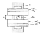
도 4는 본 발명에 따른 플라즈마 디스플레이 패널을 나타낸 사시도이고, 도 5는 도 4에 도시된 플라즈마 디스플레이 패널의 수직 단면도이며, 도 6은 도 4에 도시된 플라즈마 디스플레이 패널의 개략적인 평면도이다.4 is a perspective view showing a plasma display panel according to the present invention, FIG. 5 is a vertical sectional view of the plasma display panel shown in FIG. 4, and FIG. 6 is a schematic plan view of the plasma display panel shown in FIG. 4.
도 4 내지 도 6에 도시된 바와 같이, 본 발명에 따른 플라즈마 디스플레이 패널은 상부기판(45) 상에 형성된 한 쌍의 버스 전극(44,46) 즉, 스캔 전극(44) 및 서스테인 전극(46)과, 하부기판(42) 상에 형성된 어드레스 전극(52)을 구비한다.As shown in FIGS. 4 to 6, the plasma display panel according to the present invention includes a pair of
스캔 전극(44)과 서스테인 전극(46) 각각은 양광주 영역을 폭넓게 확보하기 위하여 소정 거리로 이격된 도전성의 버스 전극(44,46)만으로 이루어지고, 각 버스 전극(44,46)은 적어도 두 개 이상의 버스 라인(44a,46a)과, 버스 라인(44a,46a)을 연결하는 연결부(44b,46b)를 포함하고, 방전공간(400)의 중심부와 가장 가까운 버스 라인(44a,46a)에는 적어도 하나 이상의 돌출부(44c,46c)가 형성되어 있다.Each of the
이를 보다 상세히 설명하면 다음과 같다.This will be described in more detail as follows.
본 발명의 실시 예에 따른 플라즈마 디스플레이 패널에서는 서스테인 방전이 일어나는 스캔 전극(44)과 서스테인 전극(46) 사이의 거리를 종래보다 멀리 위치시켜 서스테인 방전이 긴 방전 경로를 갖도록 한다.In the plasma display panel according to the exemplary embodiment of the present invention, the distance between the
즉, 종래와는 달리 본 발명의 실시 예에 따른 플라즈마 디스플레이 패널에 있어서는 스캔 전극(44)과 서스테인 전극(46) 각각에서 투명 전극을 삭제하고 도전성의 버스 전극만으로 스캔 전극(44)과 서스테인 전극(46)을 구성함으로써, 스캔 전극(44)과 서스테인 전극(46) 사이의 이격 거리를 증가시키고 이에 따라 스캔 전극(44)과 서스테인 전극(46) 사이의 방전 갭을 증가시켜 양광주영역을 폭 넓게 활용하는 것이다.That is, unlike the related art, in the plasma display panel according to the exemplary embodiment of the present invention, the transparent electrode is removed from each of the
이러한 스캔 전극(44)과 서스테인 전극(46) 사이의 이격 거리(B)는 스캔 전극(44) 또는 서스테인 전극(46)과 어드레스 전극(52) 간의 이격 거리(D)보다 크게 설정하는 것이 바람직하다.The separation distance B between the
이와 같이 스캔 전극(44)과 서스테인 전극(46) 사이의 이격 거리(B)를 스캔 전극(44) 또는 서스테인 전극(46)과 어드레스 전극(52) 간의 이격 거리(D)보다 크게 설정함으로써, 스캔 전극(44)과 서스테인 전극(46)간의 면 방전 영역을 스캔 전극(44) 또는 서스테인 전극(46)과 어드레스 전극(52) 간의 대향 방전 영역보다 크게 설정하고 이에 따라 스캔 전극(44)과 서스테인 전극(46)간의 면 방전 효율을 크게 향상시키는 것이다.Thus, by setting the separation distance B between the
이러한 스캔 전극(44)과 서스테인 전극(46) 사이의 이격 거리는 250 ㎛ 이상 450 ㎛ 이하로 하는 것이 바람직하다.The separation distance between the
이와 같이 전극 간의 거리가 멀어짐에 따라 방전 경로가 길어지므로 양광주 영역을 확대시킬 수 있게 되어 높은 방전효율을 얻을 수 있다.As the distance between the electrodes increases in this way, the discharge path becomes longer, so that the positive light column region can be enlarged, and thus high discharge efficiency can be obtained.
한편 이때, 스캔 전극(44) 및 서스테인 전극(46) 간의 방전 경로가 길어지면 두 전극(44,46) 간에 방전을 일으키기 위한 방전 전압이 높아지게 된다.In this case, when the discharge path between the
따라서 본 발명은 스캔 전극(44)과 서스테인 전극(46) 간의 방전 전압을 저감하는 수단으로 방전공간(400)의 중심부와 가장 가까운 버스 라인(44a,46a)에는 적어도 하나 이상의 돌출부(44c,46c)를 형성한다.Therefore, the present invention is a means for reducing the discharge voltage between the
이러한 돌출부(44c,46c)는 방전공간(400)의 중심부를 향하여 형성하는 것이 바람직하다. The
이와 같은 돌출부(44c,46c)로 인한 전계 집중의 효과를 이용함으로써 버스 전극 (44,46)들 즉, 스캔 전극(44)과 서스테인 전극(46) 간의 방전 전압을 저감할 수 있다.The discharge voltage between the
버스 전극(44,46) 간에 형성되는 방전 갭의 폭(B)은 버스 전극의 폭(A=C)의 1 배 이상 4 배 이하로 하는 것이 바람직하다.It is preferable that the width B of the discharge gap formed between the
이와 같이 방전 갭의 폭(B)을 버스 전극의 폭(A=C)의 1 배 이상 4 배 이하로 조정함으로써 방전 영역을 확장하여 서스테인 방전의 효율을 향상시킨다.Thus, by adjusting the width B of the discharge gap to 1 or more times and 4 times or less the width A of the bus electrode, the discharge area is expanded to improve the efficiency of the sustain discharge.
버스 전극(44,46)의 두께는 1 ㎛ 이상 10 ㎛ 이하로 하는 것이 바람직하다.The thickness of the
돌출부(44c,46c)의 형상은 다각형 또는 곡선형 중 적어도 어느 하나를 포함하도록 하는 것이 바람직하다.It is preferable that the shape of the
이와 같이 버스 전극(44,46)의 두께를 조절하거나 돌출부(44c,46c)의 형상 을 조정하여 전계를 집중시킴으로써 서스테인 방전 전압을 낮출 수 있다. Thus, the sustain discharge voltage can be lowered by concentrating the electric field by adjusting the thickness of the
한편 이러한 돌출부는 도 7에 도시된 바와 같이 다양한 여러 가지의 형태로 구성할 수 있다.Meanwhile, the protrusion may be configured in various forms as shown in FIG. 7.
또한 방전 공간(400) 상부에 위치하는 버스 전극(44,46)으로 인한 휘도의 저하를 최소화하기 위하여 버스 전극(44,46)의 구조를 적어도 두 개 이상의 버스 라인(44a,46a)과, 버스 라인을 연결하는 연결부(44b,46b)를 포함하여 구성한다. 버스 전극(44,46)의 구조를 이와 같이 설정함으로써 개구율의 감소를 막아 플라즈마 디스플레이 패널의 휘도를 확보한다.In addition, the
한편 스캔 전극(44)과 서스테인 전극(46)이 나란하게 형성된 상부기판(45)에는 상부 유전체층(50)과 보호막(48)이 적층된다.Meanwhile, an
상부 유전체층(50) 에는 플라즈마 방전시 발생된 벽전하가 축적된다.Wall charges generated during plasma discharge are accumulated in the
보호막(48)은 플라즈마 방전시 발생된 스퍼터링에 의한 상부 유전체층(50)의 손상을 방지함과 아울러 2차 전자의 방출 효율을 높이게 된다. 보호막(48)으로는 통상 산화마그네슘(MgO)이 이용된다.The
어드레스 전극(52)이 형성된 하부기판(42) 상에는 하부 유전체층(54), 격벽(56)이 형성되며, 하부 유전체층(54)과 격벽(56) 표면에는 형광체층(58)이 도포된다. 어드레스전극(52)은 스캔 전극(44) 및 서스테인 전극(46)과 교차되는 방향으로 형성된다.The lower
격벽(56)은 방전에 의해 생성된 자외선 및 가시광이 인접한 방전 셀에 누설 되는 것을 방지한다.The
형광체 층(58)은 플라즈마 방전시 발생된 자외선에 의해 여기되어 적색, 녹색 또는 청색 중 어느 하나의 가시광선을 발생하게 된다. 상/하부기판(45,42)과 격벽(56) 사이에 마련된 방전 셀의 방전공간(400)에는 방전을 위한 He+Xe, Ne+Xe 및 He+Ne+Xe 등의 불활성 혼합가스가 주입된다.The
이와 같은 구조를 갖는 본 발명에 따른 플라즈마 디스플레이 패널은 이상에서 상세히 살펴본 바와 같이 함으로써, 양광주 영역을 적극적으로 활용하여 발광효율을 높이는 한편, 방전 개시 전압을 낮추어 구동효율을 향상시킨다.Plasma display panel according to the present invention having such a structure as described above in detail, by actively utilizing the positive light column region to increase the luminous efficiency, while lowering the discharge start voltage to improve the driving efficiency.
또한 개구율의 저하를 최소화하여 휘도를 향상시킨다.In addition, the decrease in the aperture ratio is minimized to improve the brightness.
이상에서 보는 바와 같이, 상술한 본 발명의 기술적 구성은 본 발명이 속하는 기술분야의 당업자가 본 발명의 그 기술적 사상이나 필수적 특징을 변경하지 않고서 다른 구체적인 형태로 실시될 수 있다는 것을 이해할 수 있을 것이다.As described above, it will be understood by those skilled in the art that the above-described technical configuration may be implemented in other specific forms without changing the technical spirit or essential features of the present invention.
그러므로 이상에서 기술한 실시 예들은 모든 면에서 예시적인 것이며 한정적인 것이 아닌 것으로서 이해되어야 하고, 본 발명의 범위는 상세한 설명보다는 후술하는 특허청구범위에 의하여 나타내어지며, 특허청구범위의 의미 및 범위 그리고 그 등가 개념으로부터 도출되는 모든 변경 또는 변형된 형태가 본 발명의 범위에 포함되는 것으로 해석되어야 한다.Therefore, the above-described embodiments are to be understood as illustrative and not restrictive in all respects, and the scope of the present invention is indicated by the following claims rather than the detailed description, and the meaning and scope of the claims and their All changes or modifications derived from an equivalent concept should be construed as being included in the scope of the present invention.
이상에서 상세히 설명한 바와 같이, 본 발명은 개선된 전극 구조를 통하여 발광효율 및 구동효율을 향상시키는 플라즈마 디스플레이 패널을 제공한다.As described in detail above, the present invention provides a plasma display panel which improves luminous efficiency and driving efficiency through an improved electrode structure.
Claims (7)
Priority Applications (1)
| Application Number | Priority Date | Filing Date | Title |
|---|---|---|---|
| KR1020050036040A KR100692829B1 (en) | 2005-04-29 | 2005-04-29 | Plasma Display Panel |
Applications Claiming Priority (1)
| Application Number | Priority Date | Filing Date | Title |
|---|---|---|---|
| KR1020050036040A KR100692829B1 (en) | 2005-04-29 | 2005-04-29 | Plasma Display Panel |
Publications (2)
| Publication Number | Publication Date |
|---|---|
| KR20060113141A true KR20060113141A (en) | 2006-11-02 |
| KR100692829B1 KR100692829B1 (en) | 2007-03-09 |
Family
ID=37651546
Family Applications (1)
| Application Number | Title | Priority Date | Filing Date |
|---|---|---|---|
| KR1020050036040A KR100692829B1 (en) | 2005-04-29 | 2005-04-29 | Plasma Display Panel |
Country Status (1)
| Country | Link |
|---|---|
| KR (1) | KR100692829B1 (en) |
Cited By (3)
| Publication number | Priority date | Publication date | Assignee | Title |
|---|---|---|---|---|
| KR100811529B1 (en) * | 2006-12-11 | 2008-03-07 | 엘지전자 주식회사 | Plasma display panel |
| KR100850906B1 (en) * | 2006-12-11 | 2008-08-07 | 엘지전자 주식회사 | Plasma Display Panel |
| KR100850901B1 (en) * | 2006-12-08 | 2008-08-07 | 엘지전자 주식회사 | Plasma Display Panel and Plasma Display Apparatus equip with the same |
-
2005
- 2005-04-29 KR KR1020050036040A patent/KR100692829B1/en not_active IP Right Cessation
Cited By (3)
| Publication number | Priority date | Publication date | Assignee | Title |
|---|---|---|---|---|
| KR100850901B1 (en) * | 2006-12-08 | 2008-08-07 | 엘지전자 주식회사 | Plasma Display Panel and Plasma Display Apparatus equip with the same |
| KR100811529B1 (en) * | 2006-12-11 | 2008-03-07 | 엘지전자 주식회사 | Plasma display panel |
| KR100850906B1 (en) * | 2006-12-11 | 2008-08-07 | 엘지전자 주식회사 | Plasma Display Panel |
Also Published As
| Publication number | Publication date |
|---|---|
| KR100692829B1 (en) | 2007-03-09 |
Similar Documents
| Publication | Publication Date | Title |
|---|---|---|
| KR20050101427A (en) | Plasma display panel | |
| KR100692829B1 (en) | Plasma Display Panel | |
| US7781972B2 (en) | Plasma display panel | |
| KR100830311B1 (en) | Plasma display panel and manufacturing method thereof | |
| KR100603325B1 (en) | Plasma display panel | |
| US7667404B2 (en) | Plasma display apparatus | |
| KR100489875B1 (en) | Plasma display panel | |
| KR100333415B1 (en) | Plasma Display Panel | |
| KR100533722B1 (en) | Method of driving plasma display panel | |
| KR20030041054A (en) | Plasma display panel | |
| KR100625572B1 (en) | Plasma Display Panel | |
| KR100669430B1 (en) | Plasma Display Panel | |
| KR100705803B1 (en) | Plasma Display Panel | |
| KR100353953B1 (en) | Plasma Display Panel | |
| EP1517350A2 (en) | Plasma display panel and method of manufacture | |
| KR100768809B1 (en) | Discharge electrode structure of plasma display panel | |
| KR100733882B1 (en) | Plasma display panel | |
| KR20010091638A (en) | Plasma Display Panel and Discharging Method of The Same | |
| US20070152580A1 (en) | Plasma display panel (PDP) | |
| KR100669431B1 (en) | Plasma Display Panel | |
| KR100615337B1 (en) | Plasma display panel | |
| KR100487000B1 (en) | Plasma display panel | |
| KR20060105143A (en) | Flat panel display device | |
| KR20050117222A (en) | Plasma display panel | |
| KR20050022705A (en) | Plasma display panel |
Legal Events
| Date | Code | Title | Description |
|---|---|---|---|
| A201 | Request for examination | ||
| E902 | Notification of reason for refusal | ||
| E701 | Decision to grant or registration of patent right | ||
| GRNT | Written decision to grant | ||
| LAPS | Lapse due to unpaid annual fee |