KR101615990B1 - Method for manufacturing semiconductor device - Google Patents
Method for manufacturing semiconductor device Download PDFInfo
- Publication number
- KR101615990B1 KR101615990B1 KR1020117006220A KR20117006220A KR101615990B1 KR 101615990 B1 KR101615990 B1 KR 101615990B1 KR 1020117006220 A KR1020117006220 A KR 1020117006220A KR 20117006220 A KR20117006220 A KR 20117006220A KR 101615990 B1 KR101615990 B1 KR 101615990B1
- Authority
- KR
- South Korea
- Prior art keywords
- semiconductor substrate
- semiconductor
- semiconductor device
- layer
- substrate
- Prior art date
Links
- 239000004065 semiconductor Substances 0.000 title claims abstract description 682
- 238000000034 method Methods 0.000 title claims description 94
- 238000004519 manufacturing process Methods 0.000 title abstract description 110
- 239000000758 substrate Substances 0.000 claims abstract description 428
- 230000008054 signal transmission Effects 0.000 claims abstract description 4
- 239000002184 metal Substances 0.000 claims description 136
- 229910052751 metal Inorganic materials 0.000 claims description 136
- 238000010030 laminating Methods 0.000 claims description 11
- 230000003287 optical effect Effects 0.000 claims description 5
- 238000001816 cooling Methods 0.000 claims description 4
- 238000002955 isolation Methods 0.000 claims description 3
- 230000000149 penetrating effect Effects 0.000 abstract description 4
- 239000010410 layer Substances 0.000 description 281
- 239000011347 resin Substances 0.000 description 61
- 229920005989 resin Polymers 0.000 description 61
- XUIMIQQOPSSXEZ-UHFFFAOYSA-N Silicon Chemical compound [Si] XUIMIQQOPSSXEZ-UHFFFAOYSA-N 0.000 description 18
- 229910052710 silicon Inorganic materials 0.000 description 18
- 239000010703 silicon Substances 0.000 description 18
- 230000015572 biosynthetic process Effects 0.000 description 12
- 238000005530 etching Methods 0.000 description 12
- 235000012431 wafers Nutrition 0.000 description 12
- 238000012986 modification Methods 0.000 description 11
- 230000004048 modification Effects 0.000 description 11
- 229910045601 alloy Inorganic materials 0.000 description 10
- 239000000956 alloy Substances 0.000 description 10
- 238000005498 polishing Methods 0.000 description 10
- 239000000470 constituent Substances 0.000 description 9
- 238000005520 cutting process Methods 0.000 description 9
- 239000000463 material Substances 0.000 description 9
- 238000001039 wet etching Methods 0.000 description 8
- 238000010586 diagram Methods 0.000 description 7
- 239000012467 final product Substances 0.000 description 7
- 229910052718 tin Inorganic materials 0.000 description 7
- 239000012790 adhesive layer Substances 0.000 description 6
- 238000001459 lithography Methods 0.000 description 6
- 239000000853 adhesive Substances 0.000 description 5
- 230000001070 adhesive effect Effects 0.000 description 5
- 238000001312 dry etching Methods 0.000 description 5
- 238000009713 electroplating Methods 0.000 description 5
- 238000000227 grinding Methods 0.000 description 5
- 238000010438 heat treatment Methods 0.000 description 5
- 238000007689 inspection Methods 0.000 description 5
- 229910000679 solder Inorganic materials 0.000 description 5
- UMIVXZPTRXBADB-UHFFFAOYSA-N benzocyclobutene Chemical compound C1=CC=C2CCC2=C1 UMIVXZPTRXBADB-UHFFFAOYSA-N 0.000 description 4
- 238000005336 cracking Methods 0.000 description 4
- 238000000151 deposition Methods 0.000 description 4
- 230000000694 effects Effects 0.000 description 4
- 229910052709 silver Inorganic materials 0.000 description 4
- 238000004528 spin coating Methods 0.000 description 4
- 229910004298 SiO 2 Inorganic materials 0.000 description 3
- VYPSYNLAJGMNEJ-UHFFFAOYSA-N Silicium dioxide Chemical compound O=[Si]=O VYPSYNLAJGMNEJ-UHFFFAOYSA-N 0.000 description 3
- 238000007747 plating Methods 0.000 description 3
- 238000004544 sputter deposition Methods 0.000 description 3
- 229910052715 tantalum Inorganic materials 0.000 description 3
- 229910052719 titanium Inorganic materials 0.000 description 3
- OKTJSMMVPCPJKN-UHFFFAOYSA-N Carbon Chemical compound [C] OKTJSMMVPCPJKN-UHFFFAOYSA-N 0.000 description 2
- LFQSCWFLJHTTHZ-UHFFFAOYSA-N Ethanol Chemical compound CCO LFQSCWFLJHTTHZ-UHFFFAOYSA-N 0.000 description 2
- 239000002041 carbon nanotube Substances 0.000 description 2
- 229910021393 carbon nanotube Inorganic materials 0.000 description 2
- 239000003575 carbonaceous material Substances 0.000 description 2
- 238000005229 chemical vapour deposition Methods 0.000 description 2
- 229920001940 conductive polymer Polymers 0.000 description 2
- 239000004020 conductor Substances 0.000 description 2
- 239000002826 coolant Substances 0.000 description 2
- 229910052802 copper Inorganic materials 0.000 description 2
- 238000000708 deep reactive-ion etching Methods 0.000 description 2
- 230000007547 defect Effects 0.000 description 2
- 238000009792 diffusion process Methods 0.000 description 2
- 238000007772 electroless plating Methods 0.000 description 2
- 239000003822 epoxy resin Substances 0.000 description 2
- 238000011049 filling Methods 0.000 description 2
- QEWYKACRFQMRMB-UHFFFAOYSA-N fluoroacetic acid Chemical compound OC(=O)CF QEWYKACRFQMRMB-UHFFFAOYSA-N 0.000 description 2
- 238000005304 joining Methods 0.000 description 2
- 239000007788 liquid Substances 0.000 description 2
- 238000002844 melting Methods 0.000 description 2
- 230000008018 melting Effects 0.000 description 2
- 239000000203 mixture Substances 0.000 description 2
- 238000005268 plasma chemical vapour deposition Methods 0.000 description 2
- 238000001020 plasma etching Methods 0.000 description 2
- 229910021420 polycrystalline silicon Inorganic materials 0.000 description 2
- 229920000647 polyepoxide Polymers 0.000 description 2
- 229920005591 polysilicon Polymers 0.000 description 2
- 229910052721 tungsten Inorganic materials 0.000 description 2
- 239000004925 Acrylic resin Substances 0.000 description 1
- 229920000178 Acrylic resin Polymers 0.000 description 1
- ATJFFYVFTNAWJD-UHFFFAOYSA-N Tin Chemical compound [Sn] ATJFFYVFTNAWJD-UHFFFAOYSA-N 0.000 description 1
- 230000001133 acceleration Effects 0.000 description 1
- 230000005540 biological transmission Effects 0.000 description 1
- 238000003486 chemical etching Methods 0.000 description 1
- 238000011109 contamination Methods 0.000 description 1
- 239000002019 doping agent Substances 0.000 description 1
- 238000010292 electrical insulation Methods 0.000 description 1
- 239000004744 fabric Substances 0.000 description 1
- 239000000835 fiber Substances 0.000 description 1
- 229910052732 germanium Inorganic materials 0.000 description 1
- GNPVGFCGXDBREM-UHFFFAOYSA-N germanium atom Chemical compound [Ge] GNPVGFCGXDBREM-UHFFFAOYSA-N 0.000 description 1
- 239000011521 glass Substances 0.000 description 1
- 230000020169 heat generation Effects 0.000 description 1
- 239000012535 impurity Substances 0.000 description 1
- 230000010354 integration Effects 0.000 description 1
- 238000003754 machining Methods 0.000 description 1
- 238000000465 moulding Methods 0.000 description 1
- 230000003647 oxidation Effects 0.000 description 1
- 238000007254 oxidation reaction Methods 0.000 description 1
- 229920002120 photoresistant polymer Polymers 0.000 description 1
- 229920001721 polyimide Polymers 0.000 description 1
- 239000009719 polyimide resin Substances 0.000 description 1
- 238000003825 pressing Methods 0.000 description 1
- 238000003672 processing method Methods 0.000 description 1
- 239000000047 product Substances 0.000 description 1
- 230000002250 progressing effect Effects 0.000 description 1
- 230000002035 prolonged effect Effects 0.000 description 1
- 239000003870 refractory metal Substances 0.000 description 1
- 239000003507 refrigerant Substances 0.000 description 1
- 230000000630 rising effect Effects 0.000 description 1
- 229910052594 sapphire Inorganic materials 0.000 description 1
- 239000010980 sapphire Substances 0.000 description 1
- 239000000377 silicon dioxide Substances 0.000 description 1
- 239000000126 substance Substances 0.000 description 1
- 238000001947 vapour-phase growth Methods 0.000 description 1
- XLYOFNOQVPJJNP-UHFFFAOYSA-N water Substances O XLYOFNOQVPJJNP-UHFFFAOYSA-N 0.000 description 1
Images


Classifications
-
- H—ELECTRICITY
- H01—ELECTRIC ELEMENTS
- H01L—SEMICONDUCTOR DEVICES NOT COVERED BY CLASS H10
- H01L21/00—Processes or apparatus adapted for the manufacture or treatment of semiconductor or solid state devices or of parts thereof
- H01L21/70—Manufacture or treatment of devices consisting of a plurality of solid state components formed in or on a common substrate or of parts thereof; Manufacture of integrated circuit devices or of parts thereof
- H01L21/71—Manufacture of specific parts of devices defined in group H01L21/70
- H01L21/768—Applying interconnections to be used for carrying current between separate components within a device comprising conductors and dielectrics
- H01L21/76898—Applying interconnections to be used for carrying current between separate components within a device comprising conductors and dielectrics formed through a semiconductor substrate
-
- H—ELECTRICITY
- H01—ELECTRIC ELEMENTS
- H01L—SEMICONDUCTOR DEVICES NOT COVERED BY CLASS H10
- H01L23/00—Details of semiconductor or other solid state devices
- H01L23/52—Arrangements for conducting electric current within the device in operation from one component to another, i.e. interconnections, e.g. wires, lead frames
-
- B—PERFORMING OPERATIONS; TRANSPORTING
- B81—MICROSTRUCTURAL TECHNOLOGY
- B81C—PROCESSES OR APPARATUS SPECIALLY ADAPTED FOR THE MANUFACTURE OR TREATMENT OF MICROSTRUCTURAL DEVICES OR SYSTEMS
- B81C1/00—Manufacture or treatment of devices or systems in or on a substrate
- B81C1/00015—Manufacture or treatment of devices or systems in or on a substrate for manufacturing microsystems
- B81C1/00222—Integrating an electronic processing unit with a micromechanical structure
- B81C1/00238—Joining a substrate with an electronic processing unit and a substrate with a micromechanical structure
-
- H—ELECTRICITY
- H01—ELECTRIC ELEMENTS
- H01L—SEMICONDUCTOR DEVICES NOT COVERED BY CLASS H10
- H01L23/00—Details of semiconductor or other solid state devices
- H01L23/48—Arrangements for conducting electric current to or from the solid state body in operation, e.g. leads, terminal arrangements ; Selection of materials therefor
- H01L23/481—Internal lead connections, e.g. via connections, feedthrough structures
-
- H—ELECTRICITY
- H01—ELECTRIC ELEMENTS
- H01L—SEMICONDUCTOR DEVICES NOT COVERED BY CLASS H10
- H01L24/00—Arrangements for connecting or disconnecting semiconductor or solid-state bodies; Methods or apparatus related thereto
- H01L24/91—Methods for connecting semiconductor or solid state bodies including different methods provided for in two or more of groups H01L24/80 - H01L24/90
- H01L24/92—Specific sequence of method steps
-
- H—ELECTRICITY
- H01—ELECTRIC ELEMENTS
- H01L—SEMICONDUCTOR DEVICES NOT COVERED BY CLASS H10
- H01L24/00—Arrangements for connecting or disconnecting semiconductor or solid-state bodies; Methods or apparatus related thereto
- H01L24/93—Batch processes
- H01L24/94—Batch processes at wafer-level, i.e. with connecting carried out on a wafer comprising a plurality of undiced individual devices
-
- H—ELECTRICITY
- H01—ELECTRIC ELEMENTS
- H01L—SEMICONDUCTOR DEVICES NOT COVERED BY CLASS H10
- H01L25/00—Assemblies consisting of a plurality of semiconductor or other solid state devices
- H01L25/03—Assemblies consisting of a plurality of semiconductor or other solid state devices all the devices being of a type provided for in a single subclass of subclasses H10B, H10F, H10H, H10K or H10N, e.g. assemblies of rectifier diodes
- H01L25/04—Assemblies consisting of a plurality of semiconductor or other solid state devices all the devices being of a type provided for in a single subclass of subclasses H10B, H10F, H10H, H10K or H10N, e.g. assemblies of rectifier diodes the devices not having separate containers
- H01L25/065—Assemblies consisting of a plurality of semiconductor or other solid state devices all the devices being of a type provided for in a single subclass of subclasses H10B, H10F, H10H, H10K or H10N, e.g. assemblies of rectifier diodes the devices not having separate containers the devices being of a type provided for in group H10D89/00
- H01L25/0657—Stacked arrangements of devices
-
- H—ELECTRICITY
- H01—ELECTRIC ELEMENTS
- H01L—SEMICONDUCTOR DEVICES NOT COVERED BY CLASS H10
- H01L25/00—Assemblies consisting of a plurality of semiconductor or other solid state devices
- H01L25/03—Assemblies consisting of a plurality of semiconductor or other solid state devices all the devices being of a type provided for in a single subclass of subclasses H10B, H10F, H10H, H10K or H10N, e.g. assemblies of rectifier diodes
- H01L25/04—Assemblies consisting of a plurality of semiconductor or other solid state devices all the devices being of a type provided for in a single subclass of subclasses H10B, H10F, H10H, H10K or H10N, e.g. assemblies of rectifier diodes the devices not having separate containers
- H01L25/07—Assemblies consisting of a plurality of semiconductor or other solid state devices all the devices being of a type provided for in a single subclass of subclasses H10B, H10F, H10H, H10K or H10N, e.g. assemblies of rectifier diodes the devices not having separate containers the devices being of a type provided for in group subclass H10D
-
- H—ELECTRICITY
- H01—ELECTRIC ELEMENTS
- H01L—SEMICONDUCTOR DEVICES NOT COVERED BY CLASS H10
- H01L25/00—Assemblies consisting of a plurality of semiconductor or other solid state devices
- H01L25/50—Multistep manufacturing processes of assemblies consisting of devices, the devices being individual devices of subclass H10D or integrated devices of class H10
-
- B—PERFORMING OPERATIONS; TRANSPORTING
- B81—MICROSTRUCTURAL TECHNOLOGY
- B81B—MICROSTRUCTURAL DEVICES OR SYSTEMS, e.g. MICROMECHANICAL DEVICES
- B81B2207/00—Microstructural systems or auxiliary parts thereof
- B81B2207/07—Interconnects
-
- B—PERFORMING OPERATIONS; TRANSPORTING
- B81—MICROSTRUCTURAL TECHNOLOGY
- B81C—PROCESSES OR APPARATUS SPECIALLY ADAPTED FOR THE MANUFACTURE OR TREATMENT OF MICROSTRUCTURAL DEVICES OR SYSTEMS
- B81C2201/00—Manufacture or treatment of microstructural devices or systems
- B81C2201/01—Manufacture or treatment of microstructural devices or systems in or on a substrate
- B81C2201/0174—Manufacture or treatment of microstructural devices or systems in or on a substrate for making multi-layered devices, film deposition or growing
- B81C2201/019—Bonding or gluing multiple substrate layers
-
- B—PERFORMING OPERATIONS; TRANSPORTING
- B81—MICROSTRUCTURAL TECHNOLOGY
- B81C—PROCESSES OR APPARATUS SPECIALLY ADAPTED FOR THE MANUFACTURE OR TREATMENT OF MICROSTRUCTURAL DEVICES OR SYSTEMS
- B81C2203/00—Forming microstructural systems
- B81C2203/07—Integrating an electronic processing unit with a micromechanical structure
- B81C2203/0785—Transfer and j oin technology, i.e. forming the electronic processing unit and the micromechanical structure on separate substrates and joining the substrates
- B81C2203/0792—Forming interconnections between the electronic processing unit and the micromechanical structure
-
- H—ELECTRICITY
- H01—ELECTRIC ELEMENTS
- H01L—SEMICONDUCTOR DEVICES NOT COVERED BY CLASS H10
- H01L2221/00—Processes or apparatus adapted for the manufacture or treatment of semiconductor or solid state devices or of parts thereof covered by H01L21/00
- H01L2221/67—Apparatus for handling semiconductor or electric solid state devices during manufacture or treatment thereof; Apparatus for handling wafers during manufacture or treatment of semiconductor or electric solid state devices or components; Apparatus not specifically provided for elsewhere
- H01L2221/683—Apparatus for handling semiconductor or electric solid state devices during manufacture or treatment thereof; Apparatus for handling wafers during manufacture or treatment of semiconductor or electric solid state devices or components; Apparatus not specifically provided for elsewhere for supporting or gripping
- H01L2221/68304—Apparatus for handling semiconductor or electric solid state devices during manufacture or treatment thereof; Apparatus for handling wafers during manufacture or treatment of semiconductor or electric solid state devices or components; Apparatus not specifically provided for elsewhere for supporting or gripping using temporarily an auxiliary support
- H01L2221/68345—Apparatus for handling semiconductor or electric solid state devices during manufacture or treatment thereof; Apparatus for handling wafers during manufacture or treatment of semiconductor or electric solid state devices or components; Apparatus not specifically provided for elsewhere for supporting or gripping using temporarily an auxiliary support used as a support during the manufacture of self supporting substrates
-
- H—ELECTRICITY
- H01—ELECTRIC ELEMENTS
- H01L—SEMICONDUCTOR DEVICES NOT COVERED BY CLASS H10
- H01L2221/00—Processes or apparatus adapted for the manufacture or treatment of semiconductor or solid state devices or of parts thereof covered by H01L21/00
- H01L2221/67—Apparatus for handling semiconductor or electric solid state devices during manufacture or treatment thereof; Apparatus for handling wafers during manufacture or treatment of semiconductor or electric solid state devices or components; Apparatus not specifically provided for elsewhere
- H01L2221/683—Apparatus for handling semiconductor or electric solid state devices during manufacture or treatment thereof; Apparatus for handling wafers during manufacture or treatment of semiconductor or electric solid state devices or components; Apparatus not specifically provided for elsewhere for supporting or gripping
- H01L2221/68304—Apparatus for handling semiconductor or electric solid state devices during manufacture or treatment thereof; Apparatus for handling wafers during manufacture or treatment of semiconductor or electric solid state devices or components; Apparatus not specifically provided for elsewhere for supporting or gripping using temporarily an auxiliary support
- H01L2221/68377—Apparatus for handling semiconductor or electric solid state devices during manufacture or treatment thereof; Apparatus for handling wafers during manufacture or treatment of semiconductor or electric solid state devices or components; Apparatus not specifically provided for elsewhere for supporting or gripping using temporarily an auxiliary support with parts of the auxiliary support remaining in the finished device
-
- H—ELECTRICITY
- H01—ELECTRIC ELEMENTS
- H01L—SEMICONDUCTOR DEVICES NOT COVERED BY CLASS H10
- H01L2224/00—Indexing scheme for arrangements for connecting or disconnecting semiconductor or solid-state bodies and methods related thereto as covered by H01L24/00
- H01L2224/01—Means for bonding being attached to, or being formed on, the surface to be connected, e.g. chip-to-package, die-attach, "first-level" interconnects; Manufacturing methods related thereto
- H01L2224/10—Bump connectors; Manufacturing methods related thereto
- H01L2224/12—Structure, shape, material or disposition of the bump connectors prior to the connecting process
- H01L2224/13—Structure, shape, material or disposition of the bump connectors prior to the connecting process of an individual bump connector
- H01L2224/13001—Core members of the bump connector
- H01L2224/13005—Structure
- H01L2224/13009—Bump connector integrally formed with a via connection of the semiconductor or solid-state body
-
- H—ELECTRICITY
- H01—ELECTRIC ELEMENTS
- H01L—SEMICONDUCTOR DEVICES NOT COVERED BY CLASS H10
- H01L2224/00—Indexing scheme for arrangements for connecting or disconnecting semiconductor or solid-state bodies and methods related thereto as covered by H01L24/00
- H01L2224/01—Means for bonding being attached to, or being formed on, the surface to be connected, e.g. chip-to-package, die-attach, "first-level" interconnects; Manufacturing methods related thereto
- H01L2224/10—Bump connectors; Manufacturing methods related thereto
- H01L2224/15—Structure, shape, material or disposition of the bump connectors after the connecting process
- H01L2224/16—Structure, shape, material or disposition of the bump connectors after the connecting process of an individual bump connector
- H01L2224/161—Disposition
- H01L2224/16135—Disposition the bump connector connecting between different semiconductor or solid-state bodies, i.e. chip-to-chip
- H01L2224/16145—Disposition the bump connector connecting between different semiconductor or solid-state bodies, i.e. chip-to-chip the bodies being stacked
-
- H—ELECTRICITY
- H01—ELECTRIC ELEMENTS
- H01L—SEMICONDUCTOR DEVICES NOT COVERED BY CLASS H10
- H01L2224/00—Indexing scheme for arrangements for connecting or disconnecting semiconductor or solid-state bodies and methods related thereto as covered by H01L24/00
- H01L2224/01—Means for bonding being attached to, or being formed on, the surface to be connected, e.g. chip-to-package, die-attach, "first-level" interconnects; Manufacturing methods related thereto
- H01L2224/26—Layer connectors, e.g. plate connectors, solder or adhesive layers; Manufacturing methods related thereto
- H01L2224/31—Structure, shape, material or disposition of the layer connectors after the connecting process
- H01L2224/32—Structure, shape, material or disposition of the layer connectors after the connecting process of an individual layer connector
- H01L2224/321—Disposition
- H01L2224/32135—Disposition the layer connector connecting between different semiconductor or solid-state bodies, i.e. chip-to-chip
- H01L2224/32145—Disposition the layer connector connecting between different semiconductor or solid-state bodies, i.e. chip-to-chip the bodies being stacked
-
- H—ELECTRICITY
- H01—ELECTRIC ELEMENTS
- H01L—SEMICONDUCTOR DEVICES NOT COVERED BY CLASS H10
- H01L2224/00—Indexing scheme for arrangements for connecting or disconnecting semiconductor or solid-state bodies and methods related thereto as covered by H01L24/00
- H01L2224/80—Methods for connecting semiconductor or other solid state bodies using means for bonding being attached to, or being formed on, the surface to be connected
- H01L2224/83—Methods for connecting semiconductor or other solid state bodies using means for bonding being attached to, or being formed on, the surface to be connected using a layer connector
- H01L2224/83001—Methods for connecting semiconductor or other solid state bodies using means for bonding being attached to, or being formed on, the surface to be connected using a layer connector involving a temporary auxiliary member not forming part of the bonding apparatus
- H01L2224/83005—Methods for connecting semiconductor or other solid state bodies using means for bonding being attached to, or being formed on, the surface to be connected using a layer connector involving a temporary auxiliary member not forming part of the bonding apparatus being a temporary or sacrificial substrate
-
- H—ELECTRICITY
- H01—ELECTRIC ELEMENTS
- H01L—SEMICONDUCTOR DEVICES NOT COVERED BY CLASS H10
- H01L2224/00—Indexing scheme for arrangements for connecting or disconnecting semiconductor or solid-state bodies and methods related thereto as covered by H01L24/00
- H01L2224/80—Methods for connecting semiconductor or other solid state bodies using means for bonding being attached to, or being formed on, the surface to be connected
- H01L2224/83—Methods for connecting semiconductor or other solid state bodies using means for bonding being attached to, or being formed on, the surface to be connected using a layer connector
- H01L2224/838—Bonding techniques
- H01L2224/8385—Bonding techniques using a polymer adhesive, e.g. an adhesive based on silicone, epoxy, polyimide, polyester
-
- H—ELECTRICITY
- H01—ELECTRIC ELEMENTS
- H01L—SEMICONDUCTOR DEVICES NOT COVERED BY CLASS H10
- H01L2224/00—Indexing scheme for arrangements for connecting or disconnecting semiconductor or solid-state bodies and methods related thereto as covered by H01L24/00
- H01L2224/91—Methods for connecting semiconductor or solid state bodies including different methods provided for in two or more of groups H01L2224/80 - H01L2224/90
- H01L2224/92—Specific sequence of method steps
- H01L2224/9202—Forming additional connectors after the connecting process
-
- H—ELECTRICITY
- H01—ELECTRIC ELEMENTS
- H01L—SEMICONDUCTOR DEVICES NOT COVERED BY CLASS H10
- H01L2225/00—Details relating to assemblies covered by the group H01L25/00 but not provided for in its subgroups
- H01L2225/03—All the devices being of a type provided for in the same main group of the same subclass of class H10, e.g. assemblies of rectifier diodes
- H01L2225/04—All the devices being of a type provided for in the same main group of the same subclass of class H10, e.g. assemblies of rectifier diodes the devices not having separate containers
- H01L2225/065—All the devices being of a type provided for in the same main group of the same subclass of class H10
- H01L2225/06503—Stacked arrangements of devices
- H01L2225/06541—Conductive via connections through the device, e.g. vertical interconnects, through silicon via [TSV]
-
- H—ELECTRICITY
- H01—ELECTRIC ELEMENTS
- H01L—SEMICONDUCTOR DEVICES NOT COVERED BY CLASS H10
- H01L2225/00—Details relating to assemblies covered by the group H01L25/00 but not provided for in its subgroups
- H01L2225/03—All the devices being of a type provided for in the same main group of the same subclass of class H10, e.g. assemblies of rectifier diodes
- H01L2225/04—All the devices being of a type provided for in the same main group of the same subclass of class H10, e.g. assemblies of rectifier diodes the devices not having separate containers
- H01L2225/065—All the devices being of a type provided for in the same main group of the same subclass of class H10
- H01L2225/06503—Stacked arrangements of devices
- H01L2225/06589—Thermal management, e.g. cooling
-
- H—ELECTRICITY
- H01—ELECTRIC ELEMENTS
- H01L—SEMICONDUCTOR DEVICES NOT COVERED BY CLASS H10
- H01L2924/00—Indexing scheme for arrangements or methods for connecting or disconnecting semiconductor or solid-state bodies as covered by H01L24/00
- H01L2924/01—Chemical elements
- H01L2924/01004—Beryllium [Be]
-
- H—ELECTRICITY
- H01—ELECTRIC ELEMENTS
- H01L—SEMICONDUCTOR DEVICES NOT COVERED BY CLASS H10
- H01L2924/00—Indexing scheme for arrangements or methods for connecting or disconnecting semiconductor or solid-state bodies as covered by H01L24/00
- H01L2924/01—Chemical elements
- H01L2924/01005—Boron [B]
-
- H—ELECTRICITY
- H01—ELECTRIC ELEMENTS
- H01L—SEMICONDUCTOR DEVICES NOT COVERED BY CLASS H10
- H01L2924/00—Indexing scheme for arrangements or methods for connecting or disconnecting semiconductor or solid-state bodies as covered by H01L24/00
- H01L2924/01—Chemical elements
- H01L2924/01006—Carbon [C]
-
- H—ELECTRICITY
- H01—ELECTRIC ELEMENTS
- H01L—SEMICONDUCTOR DEVICES NOT COVERED BY CLASS H10
- H01L2924/00—Indexing scheme for arrangements or methods for connecting or disconnecting semiconductor or solid-state bodies as covered by H01L24/00
- H01L2924/01—Chemical elements
- H01L2924/01013—Aluminum [Al]
-
- H—ELECTRICITY
- H01—ELECTRIC ELEMENTS
- H01L—SEMICONDUCTOR DEVICES NOT COVERED BY CLASS H10
- H01L2924/00—Indexing scheme for arrangements or methods for connecting or disconnecting semiconductor or solid-state bodies as covered by H01L24/00
- H01L2924/01—Chemical elements
- H01L2924/01019—Potassium [K]
-
- H—ELECTRICITY
- H01—ELECTRIC ELEMENTS
- H01L—SEMICONDUCTOR DEVICES NOT COVERED BY CLASS H10
- H01L2924/00—Indexing scheme for arrangements or methods for connecting or disconnecting semiconductor or solid-state bodies as covered by H01L24/00
- H01L2924/01—Chemical elements
- H01L2924/01024—Chromium [Cr]
-
- H—ELECTRICITY
- H01—ELECTRIC ELEMENTS
- H01L—SEMICONDUCTOR DEVICES NOT COVERED BY CLASS H10
- H01L2924/00—Indexing scheme for arrangements or methods for connecting or disconnecting semiconductor or solid-state bodies as covered by H01L24/00
- H01L2924/01—Chemical elements
- H01L2924/01029—Copper [Cu]
-
- H—ELECTRICITY
- H01—ELECTRIC ELEMENTS
- H01L—SEMICONDUCTOR DEVICES NOT COVERED BY CLASS H10
- H01L2924/00—Indexing scheme for arrangements or methods for connecting or disconnecting semiconductor or solid-state bodies as covered by H01L24/00
- H01L2924/01—Chemical elements
- H01L2924/01032—Germanium [Ge]
-
- H—ELECTRICITY
- H01—ELECTRIC ELEMENTS
- H01L—SEMICONDUCTOR DEVICES NOT COVERED BY CLASS H10
- H01L2924/00—Indexing scheme for arrangements or methods for connecting or disconnecting semiconductor or solid-state bodies as covered by H01L24/00
- H01L2924/01—Chemical elements
- H01L2924/01033—Arsenic [As]
-
- H—ELECTRICITY
- H01—ELECTRIC ELEMENTS
- H01L—SEMICONDUCTOR DEVICES NOT COVERED BY CLASS H10
- H01L2924/00—Indexing scheme for arrangements or methods for connecting or disconnecting semiconductor or solid-state bodies as covered by H01L24/00
- H01L2924/01—Chemical elements
- H01L2924/01046—Palladium [Pd]
-
- H—ELECTRICITY
- H01—ELECTRIC ELEMENTS
- H01L—SEMICONDUCTOR DEVICES NOT COVERED BY CLASS H10
- H01L2924/00—Indexing scheme for arrangements or methods for connecting or disconnecting semiconductor or solid-state bodies as covered by H01L24/00
- H01L2924/01—Chemical elements
- H01L2924/01047—Silver [Ag]
-
- H—ELECTRICITY
- H01—ELECTRIC ELEMENTS
- H01L—SEMICONDUCTOR DEVICES NOT COVERED BY CLASS H10
- H01L2924/00—Indexing scheme for arrangements or methods for connecting or disconnecting semiconductor or solid-state bodies as covered by H01L24/00
- H01L2924/01—Chemical elements
- H01L2924/01073—Tantalum [Ta]
-
- H—ELECTRICITY
- H01—ELECTRIC ELEMENTS
- H01L—SEMICONDUCTOR DEVICES NOT COVERED BY CLASS H10
- H01L2924/00—Indexing scheme for arrangements or methods for connecting or disconnecting semiconductor or solid-state bodies as covered by H01L24/00
- H01L2924/01—Chemical elements
- H01L2924/01074—Tungsten [W]
-
- H—ELECTRICITY
- H01—ELECTRIC ELEMENTS
- H01L—SEMICONDUCTOR DEVICES NOT COVERED BY CLASS H10
- H01L2924/00—Indexing scheme for arrangements or methods for connecting or disconnecting semiconductor or solid-state bodies as covered by H01L24/00
- H01L2924/01—Chemical elements
- H01L2924/01075—Rhenium [Re]
-
- H—ELECTRICITY
- H01—ELECTRIC ELEMENTS
- H01L—SEMICONDUCTOR DEVICES NOT COVERED BY CLASS H10
- H01L2924/00—Indexing scheme for arrangements or methods for connecting or disconnecting semiconductor or solid-state bodies as covered by H01L24/00
- H01L2924/01—Chemical elements
- H01L2924/01078—Platinum [Pt]
-
- H—ELECTRICITY
- H01—ELECTRIC ELEMENTS
- H01L—SEMICONDUCTOR DEVICES NOT COVERED BY CLASS H10
- H01L2924/00—Indexing scheme for arrangements or methods for connecting or disconnecting semiconductor or solid-state bodies as covered by H01L24/00
- H01L2924/01—Chemical elements
- H01L2924/01079—Gold [Au]
-
- H—ELECTRICITY
- H01—ELECTRIC ELEMENTS
- H01L—SEMICONDUCTOR DEVICES NOT COVERED BY CLASS H10
- H01L2924/00—Indexing scheme for arrangements or methods for connecting or disconnecting semiconductor or solid-state bodies as covered by H01L24/00
- H01L2924/01—Chemical elements
- H01L2924/01082—Lead [Pb]
-
- H—ELECTRICITY
- H01—ELECTRIC ELEMENTS
- H01L—SEMICONDUCTOR DEVICES NOT COVERED BY CLASS H10
- H01L2924/00—Indexing scheme for arrangements or methods for connecting or disconnecting semiconductor or solid-state bodies as covered by H01L24/00
- H01L2924/013—Alloys
- H01L2924/014—Solder alloys
-
- H—ELECTRICITY
- H01—ELECTRIC ELEMENTS
- H01L—SEMICONDUCTOR DEVICES NOT COVERED BY CLASS H10
- H01L2924/00—Indexing scheme for arrangements or methods for connecting or disconnecting semiconductor or solid-state bodies as covered by H01L24/00
- H01L2924/10—Details of semiconductor or other solid state devices to be connected
- H01L2924/102—Material of the semiconductor or solid state bodies
- H01L2924/1025—Semiconducting materials
- H01L2924/10251—Elemental semiconductors, i.e. Group IV
- H01L2924/10252—Germanium [Ge]
-
- H—ELECTRICITY
- H01—ELECTRIC ELEMENTS
- H01L—SEMICONDUCTOR DEVICES NOT COVERED BY CLASS H10
- H01L2924/00—Indexing scheme for arrangements or methods for connecting or disconnecting semiconductor or solid-state bodies as covered by H01L24/00
- H01L2924/10—Details of semiconductor or other solid state devices to be connected
- H01L2924/102—Material of the semiconductor or solid state bodies
- H01L2924/1025—Semiconducting materials
- H01L2924/10251—Elemental semiconductors, i.e. Group IV
- H01L2924/10253—Silicon [Si]
-
- H—ELECTRICITY
- H01—ELECTRIC ELEMENTS
- H01L—SEMICONDUCTOR DEVICES NOT COVERED BY CLASS H10
- H01L2924/00—Indexing scheme for arrangements or methods for connecting or disconnecting semiconductor or solid-state bodies as covered by H01L24/00
- H01L2924/10—Details of semiconductor or other solid state devices to be connected
- H01L2924/11—Device type
- H01L2924/14—Integrated circuits
-
- H—ELECTRICITY
- H01—ELECTRIC ELEMENTS
- H01L—SEMICONDUCTOR DEVICES NOT COVERED BY CLASS H10
- H01L2924/00—Indexing scheme for arrangements or methods for connecting or disconnecting semiconductor or solid-state bodies as covered by H01L24/00
- H01L2924/10—Details of semiconductor or other solid state devices to be connected
- H01L2924/146—Mixed devices
- H01L2924/1461—MEMS
-
- H—ELECTRICITY
- H01—ELECTRIC ELEMENTS
- H01L—SEMICONDUCTOR DEVICES NOT COVERED BY CLASS H10
- H01L2924/00—Indexing scheme for arrangements or methods for connecting or disconnecting semiconductor or solid-state bodies as covered by H01L24/00
- H01L2924/15—Details of package parts other than the semiconductor or other solid state devices to be connected
- H01L2924/151—Die mounting substrate
- H01L2924/156—Material
- H01L2924/15786—Material with a principal constituent of the material being a non metallic, non metalloid inorganic material
- H01L2924/15788—Glasses, e.g. amorphous oxides, nitrides or fluorides
Landscapes
- Engineering & Computer Science (AREA)
- Microelectronics & Electronic Packaging (AREA)
- Power Engineering (AREA)
- Computer Hardware Design (AREA)
- Physics & Mathematics (AREA)
- Condensed Matter Physics & Semiconductors (AREA)
- General Physics & Mathematics (AREA)
- Manufacturing & Machinery (AREA)
- Internal Circuitry In Semiconductor Integrated Circuit Devices (AREA)
Abstract
주면측에 반도체집적회로를 갖는 복수의 반도체칩이 형성된 반도체기판을 적층하고, 상이한 층의 상기 반도체기판을 구성하는 상기 반도체칩끼리를 신호전달가능하게 접속하고, 그 후 상기 반도체칩 부분을 개편화하는 반도체장치의 제조방법을 제공한다. 본발명에 따른 반도체장치의 제조방법은 제 1 반도체기판 및 제 2 반도체기판을 준비하는 제 1 공정과, 상기 제 2 반도체기판을 박형화하는 제 2 공정과, 박형화된 상기 제 2 반도체기판의 주면과 반대측의 면을 절연층을 통하여 상기 제 1 반도체기판의 주면에 고착하는 제 3 공정과, 박형화된 상기 제 2 반도체기판에 상기 제 2 반도체기판의 주면에서 상기 주면과 반대측의 면을 관통하는 비아홀을 형성하는 제 4 공정과, 상기 비아홀을 통하여 상기 제 1 반도체기판의 상기 반도체칩과 상기 제 2 반도체기판의 상기 반도체칩 사이의 신호전달을 가능하게 하는 접속부를 형성하는 제 5 공정을 갖는다.A semiconductor substrate having a plurality of semiconductor chips each having a semiconductor integrated circuit formed on its main surface side is laminated and the semiconductor chips constituting the semiconductor substrate of different layers are connected to each other so as to transmit signals, The present invention also provides a method of manufacturing a semiconductor device. A method of manufacturing a semiconductor device according to the present invention includes a first step of preparing a first semiconductor substrate and a second semiconductor substrate, a second step of thinning the second semiconductor substrate, a step of forming a thinned- A third step of bonding the opposite surface of the second semiconductor substrate to the main surface of the first semiconductor substrate through an insulating layer, and a third step of forming a via hole penetrating the surface of the second semiconductor substrate opposite to the main surface, And a fifth step of forming a connection portion enabling signal transmission between the semiconductor chip of the first semiconductor substrate and the semiconductor chip of the second semiconductor substrate via the via hole.
Description
본발명은 반도체장치의 제조방법에 관한 것으로, 특히, 복수의 반도체칩이 형성된 반도체기판을 적층하고, 상이한 층의 반도체기판을 구성하는 반도체칩끼리를 신호전달가능하게 접속하고, 그 후 반도체칩 부분을 개편화하는 반도체장치의 제조방법에 관한 것이다.More particularly, the present invention relates to a method of manufacturing a semiconductor device, in which a semiconductor substrate on which a plurality of semiconductor chips are formed is stacked, semiconductor chips constituting semiconductor substrates of different layers are connected to each other so as to transmit signals, To a method of manufacturing a semiconductor device.
최근 들어 반도체응용제품은 디지털카메라나 휴대전화 등의 각종 모바일기기 용도 등으로서 소형화, 박형화, 경량화가 급격히 진행되고 있다. 그에 따라, 반도체응용제품에 탑재되는 반도체장치에도 소형화, 고밀도화가 요구되고, 그 요구에 대응하기 위하여, 예를 들어, 복수의 반도체칩이 형성된 반도체기판(웨이퍼)을 반도체기판(웨이퍼)의 상태로 복수개 적층하여 접합하는 웨이퍼 온 웨이퍼(Wafer On Wafer, 이하 "WOW"라고 한다) 구조의 반도체장치의 제조방법이 제안되어 있다.2. Description of the Related Art In recent years, miniaturization, thinning, and lightening of semiconductor applications have been progressing rapidly for various mobile devices such as digital cameras and mobile phones. Accordingly, a semiconductor device mounted on a semiconductor application product is required to be downsized and densified. In order to meet such a demand, for example, a semiconductor substrate (wafer) on which a plurality of semiconductor chips are formed is placed in a state of a semiconductor substrate (Hereinafter referred to as "WOW") structure in which a plurality of wafers are laminated and joined together.
이하, 도면을 참조하여 종래부터 제안되어 있는 WOW구조의 반도체장치의 제조방법에 대하여 간단하게 설명한다. 도 1a~도 1g는 종래의 WOW구조의 반도체장치의 제조공정을 예시하는 도면이다.Hereinafter, a method of manufacturing a semiconductor device having a WOW structure that has been conventionally proposed will be briefly described with reference to the drawings. 1A to 1G are diagrams illustrating a manufacturing process of a semiconductor device of a conventional WOW structure.
먼저, 도 1a에 나타낸 공정에서는 반도체기판(110)을 준비한다. 반도체기판(110)은 기판본체(120)와 반도체집적회로(130)와 금속이 충전된 비아홀(140)을 갖는다. 기판본체(120)상에는 반도체집적회로(130)가 형성되고, 기판본체(120) 및 반도체집적회로(130)에는 금속이 충전된 비아홀(140)이 형성되어 있다. 반도체기판(110)을 준비할 때에, 기판본체(120)에 먼저 비아홀(140)을 형성한 후 반도체집적회로(130)를 형성하여도 되고, 기판본체(120)에 반도체집적회로(130)를 형성한 후 비아홀(140)을 형성하여도 된다. 또한, 기판본체(120)는 후술하는 공정에서 박형화되기 때문에, 비아홀(140)은 기판본체(120)를 관통하고 있지 않아도 된다.First, a
다음으로, 도 1b에 나타낸 공정에서는 반도체기판(110)의 반도체집적회로(130)측에 지지체(300)를 접합한다. 지지체(300)로서는, 예를 들어, 유리기판 등을 사용할 수 있다. 다음으로, 도 1c에 나타낸 공정에서는 기판본체(120)을 박형화한다. 박형화는 예를 들어, 기판본체(120)의 반도체집적회로(130)가 형성되어 있지 않은 쪽의 면을 연마함으로써 실시한다. 박형화 후의 반도체기판(110) 및 기판본체(120)를 반도체기판(110a) 및 기판본체(120a)라고 칭한다. 지지체(300)는 박형화되어 강성이 저하된 반도체기판(110a)를 지지하는 기능을 갖는다. 다음으로, 박형화된 측의 면으로부터 노출하는 비아홀(140)에 범프(미도시)를 형성한다. 또한, 범프(미도시)는 전극패드(미도시)를 통하여 형성하여도 된다.Next, in the step shown in FIG. 1B, the
다음으로, 도 1d에 나타낸 공정에서는 반도체기판(210)을 준비한다. 반도체기판(210)은 기판본체(220)와 반도체집적회로(230)와 금속이 충전된 비아홀(240)을 갖는다. 기판본체(220)상에는 반도체집적회로(230)가 형성되고, 기판본체(220) 및 반도체집적회로(230)에는 금속이 충전된 비아홀(240)이 형성되어 있다. 반도체집적회로(230)측의 면으로부터 노출하는 비아홀(240)에는 범프(미도시)가 형성되어 있다. 또한, 범프(미도시)는 전극패드(미도시)를 통하여 형성되는 경우도 있다. 그리고, 반도체기판(210)의 반도체집적회로(230)와 반도체기판(110a)의 기판본체(120a)가 대향하도록, 반도체기판(210)을 반도체기판(110a)에 접합한다. 또한, 비아홀(240)은 비아홀(140)에 대응하는 위치에 미리 형성되어 있고, 비아홀(240)과 비아홀(140)은 범프를 통하여 전기적으로 접속된다.Next, in the process shown in FIG. 1D, a
다음으로, 도 1e에 나타낸 공정에서는 도 1c와 동일한 공정에 의해 기판본체(220)를 박형화한다. 박형화 후의 반도체기판(210) 및 기판본체(220)를 반도체기판(210a) 및 기판본체(220a)라고 칭한다. 다음으로, 박형화된 측의 면으로부터 노출하는 비아홀(240)에 범프(미도시)를 형성한다. 또한, 범프(미도시)는 전극패드(미도시)를 통하여 형성하여도 된다.Next, in the process shown in FIG. 1E, the
다음으로, 도 1f에 나타낸 공정에서는 도 1d 및 도 1e와 동일한 공정을 반복하고, 반도체기판(210a)의 기판본체(220a)의 하부에 반도체기판(310a) 및 반도체기판(410a)을 적층한다. 다음으로, 도 1g에 나타낸 공정에서는 도 1f에 나타낸 지지체(300)을 제거한다. 이로써, 반도체장치(100)가 완성된다. 이와 같이 하여 박형화된 반도체기판(110a, 210a, 310a 및 410a)가 반도체기판(웨이퍼)의 상태로 접합된 WOW구조의 반도체장치(100)가 제조된다.Next, in the process shown in FIG. 1F, the same processes as those of FIG. 1D and FIG. 1E are repeated, and the
도 2a~도 2c는 종래의 WOW구조의 반도체장치의 다른 제조공정을 예시하는 도면이다. 도 2a~도 2c에 있어서, 도 1a~도 1g와 동일한 부분에는 동일한 참조부호를 부여하고, 그 설명은 생략하는 경우가 있다. 먼저, 도 2a에 나타낸 공정에서는 반도체기판(510 및 610)을 준비한다. 반도체기판(510)은 기판본체(520)와 반도체집적회로(530)를 갖는다. 기판본체(520)상에는 반도체집적회로(530)가 형성되어 있다. 반도체기판(610)은 기판본체(620)와 반도체집적회로(630)를 갖는다. 기판본체(620)상에는 반도체집적회로(630)가 형성되어 있다. 그리고, 반도체기판(610)의 반도체집적회로(630)와 반도체기판(510)의 반도체집적회로(530)가 대향하도록, 반도체기판(610)을 반도체기판(510)에 접합한다.2A to 2C are diagrams illustrating another manufacturing process of the semiconductor device of the conventional WOW structure. In Figs. 2A to 2C, the same components as those in Figs. 1A to 1G are denoted by the same reference numerals, and a description thereof may be omitted. First, in the process shown in FIG. 2A,
다음으로, 도 2b에 나타낸 공정에서는 기판본체(620)를 박형화한다. 박형화는, 예를 들어, 기판본체(620)의 반도체집적회로(630)가 형성되어 있지 않은 쪽의 면을 연마함으로써 실시한다. 박형화 후의 반도체기판(610) 및 기판본체(620)를 반도체기판(610a) 및 기판본체(620a)라고 칭한다. 다음으로, 도 2c에 나타낸 공정에서는 기판본체(620a)를 관통하고, 반도체집적회로(530) 및 반도체집적회로(630)를 접속하는, 금속이 충전된 비아홀(640)을 형성한다. 이와 같이 하여, 반도체기판(510) 및 박형화된 반도체기판(610a)이 반도체기판(웨이퍼)의 상태로 접합된 WOW구조의 반도체장치(500)가 제조된다.Next, in the step shown in FIG. 2B, the substrate
[선행기술문헌][Prior Art Literature]
[특허문헌 1] 일본공개특허공보 제2008-153499호[Patent Document 1] JP-A-2008-153499
그러나, 도 1a~도 1g에 나타낸 반도체장치의 제조방법에서는, 반도체기판끼리를 접속할 때에 양쪽의 반도체기판으로부터 노출하는 비아홀에 범프를 형성하는 공정이 필요하기 때문에, 생산성이 낮고 반도체장치의 제조비용이 상승한다는 문제가 있었다.However, in the manufacturing method of the semiconductor device shown in Figs. 1A to 1G, since the step of forming the bumps in the via holes exposed from both the semiconductor substrates is required when the semiconductor substrates are connected to each other, There was a problem of rising.
또한, 도 2a~도 2c에 나타낸 반도체장치의 제조방법에서는, 반도체집적회로가 형성되어 있는 면이 대향하도록 반도체기판끼리를 접합하기 때문에, 단순히 동일한 공정을 반복하는 것만으로는 3개 이상의 반도체기판을 적층할 수 없다. 즉, 3개 이상의 반도체기판을 적층하기 위하여는 특별한 공정이 필요하기 때문에, 생산성이 낮고 반도체장치의 제조비용이 상승한다는 문제가 있었다.In the method of manufacturing a semiconductor device shown in Figs. 2A to 2C, since the semiconductor substrates are bonded together so that the surfaces on which the semiconductor integrated circuits are formed face each other, It can not be stacked. That is, since a special process is required for stacking three or more semiconductor substrates, there is a problem that the productivity is low and the manufacturing cost of the semiconductor device increases.
또한, 도 1a~도 1g 및 도 2a~도 2c에 나타낸 어느 반도체장치의 제조방법의 경우에도, 깊은 비아홀을 형성하는 경우에는, 비아홀의 구멍가공이나 금속충전의 시간이 길어지고 또한 필요한 재료가 증가하기 때문에, 반도체장치의 제조비용이 상승한다는 문제가 있었다.1A to 1G and FIGS. 2A to 2C, in the case of forming a deep via hole, the time required for hole processing of the via hole or metal filling is prolonged, There is a problem that the manufacturing cost of the semiconductor device increases.
나아가, 도 1a~도 1g 및 도 2a~도 2c에 나타낸 어느 반도체장치의 제조방법의 경우에도, 비아홀을 드라이에칭 등으로 형성할 때에 비아홀의 사이즈나 밀도로 깊이가 상이하고 비아홀 선단부분의 직경이 변한다. 그 결과, 반도체기판을 원하는 두께로 박형화했을 때에 노출하는 비아홀의 직경이 일정하지 않기 때문에, 전기적으로 접속할 때의 저항값의 편차신뢰성이 저하된다는 문제가 있었다.Further, in the case of the semiconductor device manufacturing method shown in Figs. 1A to 1G and Figs. 2A to 2C, when the via hole is formed by dry etching or the like, the depth differs depending on the size and density of the via hole, It changes. As a result, since the diameter of the via hole exposed when the semiconductor substrate is thinned to a desired thickness is not constant, there is a problem that the reliability reliability of the resistance value is deteriorated when electrically connected.
본발명은 이러한 문제점을 감안하여 완성된 것으로, 신뢰성 및 생산성이 높고 제조비용의 저감을 도모할 수 있는 반도체장치의 제조방법을 제공하는 것을 목적으로 한다.SUMMARY OF THE INVENTION It is an object of the present invention to provide a method of manufacturing a semiconductor device which is completed in view of such problems, and which has high reliability and productivity and can reduce manufacturing cost.
상기 목적을 달성하기 위하여, 본발명은 주면측에 반도체집적회로를 갖는 복수의 반도체칩이 형성된 반도체기판을 적층하고, 상이한 층의 상기 반도체기판을 구성하는 상기 반도체칩끼리를 신호전달가능하게 접속하고, 그 후 상기 반도체칩 부분을 개편화하는 반도체장치의 제조방법으로서, 제 1 반도체기판 및 제 2 반도체기판을 준비하는 제 1 공정과, 상기 제 2 반도체기판을 박형화하는 제 2 공정과, 박형화된 상기 제 2 반도체기판의 주면과 반대측의 면을 절연층을 통하여 상기 제 1 반도체기판의 주면에 고착하는 제 3 공정과, 박형화된 상기 제 2 반도체기판에 상기 제 2 반도체기판의 주면에서 상기 주면과 반대측의 면을 관통하는 비아홀을 형성하는 제 4 공정과, 상기 비아홀을 통하여 상기 제 1 반도체기판의 상기 반도체칩과 상기 제 2 반도체기판의 상기 반도체칩 사이의 신호전달을 가능하게 하는 접속부를 형성하는 제 5 공정을 갖는 것을 특징으로 한다.According to an aspect of the present invention, there is provided a semiconductor device comprising a semiconductor substrate on which a plurality of semiconductor chips having a semiconductor integrated circuit are formed on a main surface side of the semiconductor substrate, and the semiconductor chips constituting the semiconductor substrate of different layers are connected to each other And thereafter dividing the semiconductor chip portion, the method comprising: a first step of preparing a first semiconductor substrate and a second semiconductor substrate; a second step of thinning the second semiconductor substrate; A third step of fixing the surface of the second semiconductor substrate opposite to the main surface of the second semiconductor substrate to the main surface of the first semiconductor substrate through an insulating layer; A fourth step of forming a via hole penetrating the opposite side surface of the first semiconductor substrate through the via hole; And a fifth step of forming a connection portion for enabling signal transmission between the semiconductor chips.
본발명에 의하면 신뢰성 및 생산성이 높고 제조비용의 저감을 도모할 수 있는 반도체장치의 제조방법을 제공할 수 있다.According to the present invention, it is possible to provide a method of manufacturing a semiconductor device that can improve reliability and productivity and reduce manufacturing cost.
도 1a은 종래의 WOW구조의 반도체장치의 제조공정을 예시하는 도면(그 1)이다.
도 1b는 종래의 WOW구조의 반도체장치의 제조공정을 예시하는 도면(그 2)이다.
도 1c는 종래의 WOW구조의 반도체장치의 제조공정을 예시하는 도면(그 3)이다.
도 1d는 종래의 WOW구조의 반도체장치의 제조공정을 예시하는 도면(그 4)이다.
도 1e는 종래의 WOW구조의 반도체장치의 제조공정을 예시하는 도면(그 5)이다.
도 1f는 종래의 WOW구조의 반도체장치의 제조공정을 예시하는 도면(그 6)이다.
도 1g는 종래의 WOW구조의 반도체장치의 제조공정을 예시하는 도면(그 7)이다.
도 2a는 종래의 WOW구조의 반도체장치의 다른 제조공정을 예시하는 도면(그 1)이다.
도 2b는 종래의 WOW구조의 반도체장치의 다른 제조공정을 예시하는 도면(그 2)이다.
도 2c는 종래의 WOW구조의 반도체장치의 다른 제조공정을 예시하는 도면(그 3)이다.
도 3는 본발명의 제 1 실시형태에 관련된 반도체장치를 예시하는 단면도이다.
도 4a는 본발명의 제 1 실시형태에 관련된 반도체장치의 제조공정을 예시하는 도면(그 1)이다.
도 4b는 본발명의 제 1 실시형태에 관련된 반도체장치의 제조공정을 예시하는 도면(그 2)이다.
도 4c는 본발명의 제 1 실시형태에 관련된 반도체장치의 제조공정을 예시하는 도면(그 3)이다.
도 4d는 본발명의 제 1 실시형태에 관련된 반도체장치의 제조공정을 예시하는 도면(그 4)이다.
도 4e는 본발명의 제 1 실시형태에 관련된 반도체장치의 제조공정을 예시하는 도면(그 5)이다.
도 4f는 본발명의 제 1 실시형태에 관련된 반도체장치의 제조공정을 예시하는 도면(그 6)이다.
도 4g는 본발명의 제 1 실시형태에 관련된 반도체장치의 제조공정을 예시하는 도면(그 7)이다.
도 4h는 본발명의 제 1 실시형태에 관련된 반도체장치의 제조공정을 예시하는 도면(그 8)이다.
도 4i는 본발명의 제 1 실시형태에 관련된 반도체장치의 제조공정을 예시하는 도면(그 9)이다.
도 4j는 본발명의 제 1 실시형태에 관련된 반도체장치의 제조공정을 예시하는 도면(그 10)이다.
도 4k는 본발명의 제 1 실시형태에 관련된 반도체장치의 제조공정을 예시하는 도면(그 11)이다.
도 4l은 본발명의 제 1 실시형태에 관련된 반도체장치의 제조공정을 예시하는 도면(그 12)이다.
도 4m은 본발명의 제 1 실시형태에 관련된 반도체장치의 제조공정을 예시하는 도면(그 13)이다.
도 4n은 본발명의 제 1 실시형태에 관련된 반도체장치의 제조공정을 예시하는 도면(그 14)이다.
도 4o는 본발명의 제 1 실시형태에 관련된 반도체장치의 제조공정을 예시하는 도면(그 15)이다.
도 4p는 본발명의 제 1 실시형태에 관련된 반도체장치의 제조공정을 예시하는 도면(그 16)이다.
도 4q는 본발명의 제 1 실시형태에 관련된 반도체장치의 제조공정을 예시하는 도면(그 17)이다.
도 4r은 본발명의 제 1 실시형태에 관련된 반도체장치의 제조공정을 예시하는 도면(그 18)이다.
도 4s는 본발명의 제 1 실시형태에 관련된 반도체장치의 제조공정을 예시하는 도면(그 19)이다.
도 4t는 본발명의 제 1 실시형태에 관련된 반도체장치의 제조공정을 예시하는 도면(그 20)이다.
도 5a는 본발명의 제 1 실시형태의 변형예에 관련된 반도체장치의 제조공정을 예시하는 도면(그 1)이다.
도 5b는 본발명의 제 1 실시형태의 변형예에 관련된 반도체장치의 제조공정을 예시하는 도면(그 2)이다.
도 5c는 본발명의 제 1 실시형태의 변형예에 관련된 반도체장치의 제조공정을 예시하는 도면(그 3)이다.
도 5d는 본발명의 제 1 실시형태의 변형예에 관련된 반도체장치의 제조공정을 예시하는 도면(그 4)이다.
도 6은 본발명의 제 2 실시형태에 관련된 반도체장치를 예시하는 단면도이다.
도 7a는 본발명의 제 2 실시형태에 관련된 반도체장치의 제조공정을 예시하는 도면(그 1)이다.
도 7b는 본발명의 제 2 실시형태에 관련된 반도체장치의 제조공정을 예시하는 도면(그 2)이다.
도 7c는 본발명의 제 2 실시형태에 관련된 반도체장치의 제조공정을 예시하는 도면(그 3)이다.
도 7d는 본발명의 제 2 실시형태에 관련된 반도체장치의 제조공정을 예시하는 도면(그 4)이다.
도 7e는 본발명의 제 2 실시형태에 관련된 반도체장치의 제조공정을 예시하는 도면(그 5)이다.
도 7f는 본발명의 제 2 실시형태에 관련된 반도체장치의 제조공정을 예시하는 도면(그 6)이다.
도 8은 본발명의 제 3 실시형태에 관련된 반도체장치를 예시하는 단면도이다.
도 9a는 본발명의 제 3 실시형태에 관련된 반도체장치의 제조공정을 예시하는 도면(그 1)이다.
도 9b는 본발명의 제 3 실시형태에 관련된 반도체장치의 제조공정을 예시하는 도면(그 2)이다.
도 9c는 본발명의 제 3 실시형태에 관련된 반도체장치의 제조공정을 예시하는 도면(그 3)이다.
도 9d는 본발명의 제 3 실시형태에 관련된 반도체장치의 제조공정을 예시하는 도면(그 4)이다.
도 9e는 본발명의 제 3 실시형태에 관련된 반도체장치의 제조공정을 예시하는 도면(그 5)이다.
도 9f는 본발명의 제 3 실시형태에 관련된 반도체장치의 제조공정을 예시하는 도면(그 6)이다.
도 10는 본발명의 제 4 실시형태에 관련된 반도체장치를 예시하는 단면도이다.
도 11a는 본발명의 제 4 실시형태에 관련된 반도체장치의 제조공정을 예시하는 도면(그 1)이다.
도 11b는 본발명의 제 4 실시형태에 관련된 반도체장치의 제조공정을 예시하는 도면(그 2)이다.
도 11c는 본발명의 제 4 실시형태에 관련된 반도체장치의 제조공정을 예시하는 도면(그 3)이다.
도 11d는 본발명의 제 4 실시형태에 관련된 반도체장치의 제조공정을 예시하는 도면(그 4)이다.
도 11e는 본발명의 제 4 실시형태에 관련된 반도체장치의 제조공정을 예시하는 도면(그 5)이다.
도 11f는 본발명의 제 4 실시형태에 관련된 반도체장치의 제조공정을 예시하는 도면(그 6)이다.
도 11g는 본발명의 제 4 실시형태에 관련된 반도체장치의 제조공정을 예시하는 도면(그 7)이다.
도 11h는 본발명의 제 4 실시형태에 관련된 반도체장치의 제조공정을 예시하는 도면(그 8)이다.
도 12는 본발명의 제 5 실시형태에 관련된 반도체장치를 예시하는 단면도이다.
도 13은 WOW에 주지의 반도체장치의 공정까지도 포함한 반도체장치 전체의 제조공정의 플로우차트의 예이다.1A is a view (1) illustrating a manufacturing process of a semiconductor device of a conventional WOW structure.
1B is a drawing (No. 2) illustrating a manufacturing process of a semiconductor device of a conventional WOW structure.
1C is a drawing (No. 3) illustrating a manufacturing process of a semiconductor device of a conventional WOW structure.
1D is a drawing (No. 4) illustrating a manufacturing process of a semiconductor device of a conventional WOW structure.
1E is a drawing (No. 5) illustrating a manufacturing process of a semiconductor device of a conventional WOW structure.
FIG. 1F is a view (6) illustrating a manufacturing process of a semiconductor device of a conventional WOW structure.
1G is a drawing (No. 7) illustrating a manufacturing process of a semiconductor device of a conventional WOW structure.
2A is a view (No. 1) illustrating another manufacturing process of a semiconductor device of a conventional WOW structure.
2B is a view (No. 2) illustrating another manufacturing process of the semiconductor device of the conventional WOW structure.
2C is a view (No. 3) illustrating another manufacturing process of the semiconductor device of the conventional WOW structure.
3 is a cross-sectional view illustrating a semiconductor device according to the first embodiment of the present invention.
4A is a view (No. 1) illustrating the manufacturing process of the semiconductor device according to the first embodiment of the present invention.
4B is a drawing (No. 2) illustrating a manufacturing process of the semiconductor device according to the first embodiment of the present invention.
4C is a view (No. 3) illustrating the manufacturing process of the semiconductor device according to the first embodiment of the present invention.
FIG. 4D is a view (No. 4) illustrating the manufacturing process of the semiconductor device according to the first embodiment of the present invention. FIG.
4E is a view (No. 5) illustrating the manufacturing process of the semiconductor device according to the first embodiment of the present invention.
FIG. 4F is a view (6) illustrating the manufacturing process of the semiconductor device according to the first embodiment of the present invention. FIG.
FIG. 4G is a view (No. 7) illustrating the manufacturing process of the semiconductor device according to the first embodiment of the present invention. FIG.
4H is a drawing (No. 8) illustrating the manufacturing process of the semiconductor device according to the first embodiment of the present invention.
4I is a view (9) illustrating a manufacturing process of a semiconductor device according to the first embodiment of the present invention.
4J is a view (10) illustrating the manufacturing process of the semiconductor device according to the first embodiment of the present invention.
4K is a drawing (No. 11) illustrating a manufacturing process of the semiconductor device according to the first embodiment of the present invention.
FIG. 4L is a diagram (No. 12) illustrating the manufacturing process of the semiconductor device according to the first embodiment of the present invention. FIG.
FIG. 4M is a view (13) illustrating a manufacturing process of the semiconductor device according to the first embodiment of the present invention. FIG.
4n is a drawing (14) illustrating the manufacturing process of the semiconductor device according to the first embodiment of the present invention.
4O is a drawing (No. 15) illustrating the manufacturing process of the semiconductor device according to the first embodiment of the present invention.
4P is a view (No. 16) illustrating a manufacturing process of the semiconductor device according to the first embodiment of the present invention.
FIG. 4Q is a drawing (No. 17) illustrating a manufacturing process of the semiconductor device according to the first embodiment of the present invention. FIG.
4R is a drawing (18) illustrating the manufacturing process of the semiconductor device according to the first embodiment of the present invention.
Fig. 4S is a drawing (19) illustrating the manufacturing process of the semiconductor device according to the first embodiment of the present invention. Fig.
4T is a view (20) illustrating the manufacturing process of the semiconductor device according to the first embodiment of the present invention.
5A is a view (1) illustrating a manufacturing process of a semiconductor device according to a modification of the first embodiment of the present invention.
FIG. 5B is a view (No. 2) illustrating a manufacturing process of a semiconductor device according to a modification of the first embodiment of the present invention. FIG.
FIG. 5C is a view (No. 3) illustrating a manufacturing process of a semiconductor device according to a modification of the first embodiment of the present invention. FIG.
FIG. 5D is a view (No. 4) illustrating a manufacturing process of a semiconductor device according to a modification of the first embodiment of the present invention. FIG.
6 is a cross-sectional view illustrating a semiconductor device according to a second embodiment of the present invention.
7A is a view (No. 1) illustrating a manufacturing process of a semiconductor device according to a second embodiment of the present invention.
FIG. 7B is a drawing (No. 2) illustrating the manufacturing process of the semiconductor device according to the second embodiment of the present invention. FIG.
FIG. 7C is a view (No. 3) illustrating the manufacturing process of the semiconductor device according to the second embodiment of the present invention. FIG.
FIG. 7D is a view (No. 4) illustrating the manufacturing process of the semiconductor device according to the second embodiment of the present invention. FIG.
7E is a view (No. 5) illustrating a manufacturing process of the semiconductor device according to the second embodiment of the present invention.
FIG. 7F is a view (6) illustrating the manufacturing process of the semiconductor device according to the second embodiment of the present invention.
8 is a cross-sectional view illustrating a semiconductor device according to a third embodiment of the present invention.
9A is a view (No. 1) illustrating a manufacturing process of a semiconductor device according to a third embodiment of the present invention.
FIG. 9B is a drawing (No. 2) illustrating the manufacturing process of the semiconductor device according to the third embodiment of the present invention. FIG.
Fig. 9C is a drawing (No. 3) illustrating the manufacturing process of the semiconductor device according to the third embodiment of the present invention. Fig.
FIG. 9D is a view (No. 4) illustrating the manufacturing process of the semiconductor device according to the third embodiment of the present invention. FIG.
FIG. 9E is a view (No. 5) illustrating a manufacturing process of the semiconductor device according to the third embodiment of the present invention. FIG.
FIG. 9F is a view (No. 6) illustrating the manufacturing process of the semiconductor device according to the third embodiment of the present invention. FIG.
10 is a cross-sectional view illustrating a semiconductor device according to a fourth embodiment of the present invention.
11A is a view (No. 1) illustrating a manufacturing process of a semiconductor device according to a fourth embodiment of the present invention.
FIG. 11B is a view (No. 2) illustrating the manufacturing process of the semiconductor device according to the fourth embodiment of the present invention. FIG.
FIG. 11C is a view (No. 3) illustrating the manufacturing process of the semiconductor device according to the fourth embodiment of the present invention. FIG.
FIG. 11D is a view (No. 4) illustrating the manufacturing process of the semiconductor device according to the fourth embodiment of the present invention. FIG.
FIG. 11E is a view (No. 5) illustrating a manufacturing process of the semiconductor device according to the fourth embodiment of the present invention. FIG.
FIG. 11F is a view (No. 6) illustrating the manufacturing process of the semiconductor device according to the fourth embodiment of the present invention. FIG.
FIG. 11G is a view (No. 7) illustrating the manufacturing process of the semiconductor device according to the fourth embodiment of the present invention. FIG.
11H is a drawing (No. 8) illustrating the manufacturing process of the semiconductor device according to the fourth embodiment of the present invention.
12 is a cross-sectional view illustrating a semiconductor device according to a fifth embodiment of the present invention.
13 is an example of a flow chart of a manufacturing process of the entire semiconductor device including the well-known semiconductor device process in WOW.
이하, 도면을 참조하여 본발명을 실시하기 위한 형태에 대하여 설명한다.BEST MODE FOR CARRYING OUT THE INVENTION Hereinafter, embodiments for carrying out the present invention will be described with reference to the drawings.
〈제 1 실시형태〉≪ First Embodiment >
[본발명의 제 1 실시형태에 관련된 반도체장치의 구조][Structure of the semiconductor device according to the first embodiment of the present invention]
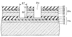
먼저, 본발명의 제 1 실시형태에 관련된 반도체장치의 구조에 대하여 설명한다. 도 3은 본발명의 제 1 실시형태에 관련된 반도체장치를 예시하는 단면도이다. 도 3을 참조하면, 본발명의 제 1 실시형태에 관련된 반도체장치(10)는 반도체기판(11c), 반도체기판(21c), 반도체기판(31c), 반도체기판(41c), 반도체기판(51c), 반도체기판(61c) 및 반도체기판(71c)이 적층된 구조를 갖는다. 반도체장치(10)는, 예를 들어, CMOS·LSI, 메모리디바이스, 센서디바이스, MEMS 등이다.First, the structure of the semiconductor device according to the first embodiment of the present invention will be described. 3 is a cross-sectional view illustrating a semiconductor device according to the first embodiment of the present invention. 3, the
반도체장치(10)를 구성하는 반도체기판(11c~71c)은, 예를 들어, 실리콘웨이퍼 등이다. 반도체기판(11c~71c)이 실리콘웨이퍼인 경우에는, 반도체장치(10)는 복수의 반도체기판(웨이퍼)이 반도체기판(웨이퍼)의 상태로 접합된 소위 WOW구조의 반도체장치이다.The
반도체기판(11c~71c)은 반도체칩이 형성되어 있는 복수의 영역 A(이하, 「반도체칩 형성영역 A」라고 한다)와 복수의 반도체칩 형성영역 A를 분리하는 스크라이브 영역 B를 갖는다. 스크라이브 영역 B에 있는 C는 다이싱블레이드 등이 반도체장치(10)를 절단하는 위치(이하, 「절단위치 C」라고 한다)를 나타내고 있다. 반도체장치(10)는 절단위치 C에서 다이싱블레이드 등에 의해 절단되어 개편화됨으로써 최종제품의 형태가 된다.The
반도체기판(11c~71c)의 각 반도체칩 형성영역 A는 기판본체(12~72, 미도시)와 반도체집적회로(13~73, 미도시)와 전극패드(15~75)를 갖는다. 기판본체(12~72, 미도시)는, 예를 들어, 실리콘 등으로 구성되어 있다. 반도체집적회로(13~73, 미도시)는, 예를 들어, 실리콘 등에 확산층(미도시), 절연층(미도시), 비아홀(미도시) 및 배선층(미도시) 등이 형성된 것이며, 기판본체(12~72, 미도시)의 한 쪽 면측에 형성되어 있다. 이후, 반도체기판(11c~71c)에 있어서 반도체집적회로(13~73, 미도시)가 형성되어 있는 측의 면을 주면이라고 칭하는 경우가 있다.Each semiconductor chip formation area A of the
전극패드(15~75)는 절연층(미도시)을 통하여 반도체집적회로(13~73, 미도시)상에 형성되어 있다. 전극패드(15~75)는 반도체집적회로(13~73, 미도시)에 형성된 배선층(미도시)과 전기적으로 접속되어 있다. 전극패드(15~75)로서는, 예를 들어, Ti층상에 Au층을 적층한 적층체 등을 사용할 수 있다. 전극패드(15~75)로서 Ni층상에 Au층을 적층한 적층체, Ni층상에 Pd층 및 Au층을 순차 적층한 적층체, Ni 대신에 Co, Ta, Ti, TiN 등의 고융점 금속으로 이루어지는 층을 이용하고 이 층상에 Cu층 혹은 Al층을 적층한 적층체 혹은 다마신(damascene) 구조형상의 배선 등을 이용하여도 된다.The
반도체기판(11c)과 반도체기판(21c)은 수지층(16)을 통하여 접합되어 있고, 반도체기판(11c)의 전극패드(15)와 반도체기판(21c)의 전극패드(25)는 비아홀(21y)에 충전된 금속층(38)을 통하여 전기적으로 접속되어 있다. 반도체기판(21c)와 반도체기판(31c)은 수지층(26)을 통하여 접합되어 있고, 반도체기판(21c)의 전극패드(25)와 반도체기판(31c)의 전극패드(35)는 비아홀(31y)에 충전된 금속층(48)을 통하여 전기적으로 접속되어 있다. 또한, 비아홀은 반도체기판간(인접하는 반도체기판 사이로 한정되지 않는다)을 접속하기 위하여 형성된 접속구멍이며, 내부에 금속층이나 광도파로 등이 형성됨으로써 반도체기판끼리를 신호전달가능하게 접속한다. 비아홀 내부에 형성된 금속층이나 광도파로 등을 접속부라고 칭하는 경우가 있다.The
반도체기판(31c)과 반도체기판(41c)은 수지층(36)을 통하여 접합되어 있고, 반도체기판(31c)의 전극패드(35)와 반도체기판(41c)의 전극패드(45)는 비아홀(41y)에 충전된 금속층(58)을 통하여 전기적으로 접속되어 있다. 반도체기판(41c)과 반도체기판(51c)은 수지층(46)을 통하여 접합되어 있고, 반도체기판(41c)의 전극패드(45)와 반도체기판(51c)의 전극패드(55)는 비아홀(51y)에 충전된 금속층(68)을 통하여 전기적으로 접속되어 있다.The
반도체기판(51c)과 반도체기판(61c)는 수지층(56)을 통하여 접합되어 있고, 반도체기판(51c)의 전극패드(55)와 반도체기판(61c)의 전극패드(65)는 비아홀(61y)에 충전된 금속층(78)을 통하여 전기적으로 접속되어 있다. 반도체기판(61c)과 반도체기판(71c)은 수지층(66)을 통하여 접합되어 있고, 반도체기판(61c)의 전극패드(65)와 반도체기판(71c)의 전극패드(75)는 비아홀(71y)에 충전된 금속층(88)을 통하여 전기적으로 접속되어 있다.The
반도체기판(71c)에는 개구부(76x)를 갖는 솔더레지스트층(76)이 형성되어 있고, 개구부(76x)내에는 외부접속단자(91)가 형성되어 있다. 외부접속단자(91)는 반도체장치(10)와 반도체장치(10)의 외부에 형성된 배선기판 등을 전기적으로 접속하기 위하여 형성된 단자이고, 전극패드(75)와 전기적으로 접속되어 있다. 외부접속단자(91)로는 땜납볼, Au범프, 도전성페이스트 등을 사용할 수 있다. 외부접속단자(91)로서 땜납볼을 사용한 경우에는, 외부접속단자(91)의 재료로는, 예를 들어, Pb를 포함하는 합금, Sn과 Cu의 합금, Sn과 Ag의 합금, Sn과 Ag와 Cu의 합금 등을 사용할 수 있다.A solder resist
[본발명의 제 1 실시형태에 관련된 반도체장치의 제조공정][Manufacturing process of semiconductor device according to the first embodiment of the present invention]
다음으로, 본발명의 제 1 실시형태에 관련된 반도체장치의 제조공정에 대하여 설명한다. 도 4a~도 4t는 본발명의 제 1 실시형태에 관련된 반도체장치의 제조공정을 예시하는 도면이다. 도 4a~도 4t에 있어서, 도 3에 나타낸 반도체장치(10)와 동일한 구성부분에는 동일한 참조부호를 부여하고, 그 설명을 생략하는 경우가 있다.Next, a manufacturing process of the semiconductor device according to the first embodiment of the present invention will be described. 4A to 4T are views illustrating a manufacturing process of the semiconductor device according to the first embodiment of the present invention. In Figs. 4A to 4T, the same constituent parts as those of the
먼저, 도 4a 및 도 4b에 나타낸 반도체기판(11)을 준비한다. 도 4a는 평면도이고, 도 4b는 단면도이다. 도 4a 및 도 4b를 참조하면, 반도체기판(11)은 기판본체(12)와 반도체집적회로(13)와 전극패드(15)를 갖는다. 다만, 도 4a에서는 전극패드(15)가 생략되어 있다. 또한, 도 4b에 있어서, 참조부호 11a는 반도체기판(11)의 한 쪽 면(전극패드(15)가 형성되어 있는 쪽의 면; 주면)을 나타내고, 참조부호 11b는 반도체기판(11)의 다른 쪽 면(주면과 반대측의 면)을 나타내고 있다.First, the
기판본체(12)는, 예를 들어, 실리콘 등으로 구성되어 있다. 반도체집적회로(13)는, 예를 들어, 실리콘 등에 확산층(미도시), 절연층(미도시), 비아홀(미도시) 및 배선층(미도시) 등이 형성된 것이다. 전극패드(15)는 절연층(미도시)을 통하여 반도체집적회로(13)상에 형성되어 있다. 전극패드(15)는 반도체집적회로(13)에 형성된 배선층(미도시)과 전기적으로 접속되어 있다. 전극패드(15)로는, 예를 들어, Ti층상에 Au층을 적층한 적층체 등을 사용할 수 있다. 또한, 전극패드(15)로서 Ni층상에 Au층을 적층한 적층체, Ni층상에 Pd층 및 Au층을 순차 적층한 적층체, Ni대신에 Co, Ta, Ti, TiN 등의 고융점 금속으로 이루어지는 층을 이용하고 이 층상에 Cu층 혹은 Al층을 적층한 적층체 혹은 다마신 구조형상의 배선 등을 이용하여도 된다.The substrate
반도체기판(11)은 복수의 반도체칩 형성영역 A와 복수의 반도체칩 형성영역 A를 분리하는 스크라이브 영역 B를 갖는다. 스크라이브 영역 B에 있는 C는 다이싱블레이드 등이 반도체기판(11)을 절단하는 위치(이하, 「절단위치 C」라고 한다)를 나타내고 있다.The
반도체기판(11)의 직경(φ1)은, 예를 들어, 6인치(약 150㎜), 8인치(약 200㎜), 12인치(약 300㎜) 등이다. 반도체기판(11)의 두께(T1)는, 예를 들어, 0.625㎜(φ1=6인치의 경우), 0.725㎜(φ1=8인치의 경우), 0.775㎜(φ1=12인치의 경우) 등이다. 본실시형태에서는 반도체기판(11)으로서 8인치(약 200㎜)의 실리콘웨이퍼를 사용한 경우를 예를 들어 이하에서 설명한다.The
다음으로, 도 4c에 나타낸 공정에서는, 도 4a 및 도 4b에 나타낸 반도체기판(11)의 바깥가장자리부(11x)를 제거한다. 바깥가장자리부(11x)를 제거한 후의 반도체기판(11)을 반도체기판(11c)으로 한다. 바깥가장자리부(11x)의 제거는, 예를 들어, 바깥가장자리부(11x)를 제거한 후의 반도체기판(11c)이 평면에서 볼 때 원형이 되도록, 반도체기판(11)의 바깥가장자리부(11x)를 그라인더 등을 이용하여 연삭한다. 이 때, 드라이폴리싱이나 웨트에칭 등을 병용하여도 된다.Next, in the step shown in Fig. 4C, the outer edge portion 11x of the
여기서, 드라이폴리싱이란, 예를 들어, 실리카를 함유시킨 섬유를 압축하여 굳혀 형성한 연마포를 이용하여 표면을 깎는(연마하는) 가공방법이다. 웨트에칭이란, 예를 들어, 스피너로 반도체기판(11)을 회전시키면서 플루오르초산 등을 공급하여 에칭을 실시하는 가공방법이다. 바깥가장자리부(11x)를 제거한 후의 반도체기판(11c)을, 예를 들어, 평면에서 볼 때 원형으로 한 경우에는, 반도체기판(11c)의 평면에서 볼 때 원형부분의 직경(φ2)은, 예를 들어, 193.0±0.1 ㎜로 할 수 있다. 이 경우, 직경(φ1)이 8인치(약 200㎜)이었던 반도체기판(11)이 소직경화 되고, 직경(φ2)이 193.0±0.1㎜의 반도체기판(11c)이 된 것으로 된다.Here, the dry polishing is a machining method for cutting (polishing) the surface using, for example, a polishing cloth formed by pressing and hardening a fiber containing silica. The wet etching is a processing method in which etching is performed by supplying fluoroacetic acid or the like while rotating the
다음으로, 도 4d에 나타낸 공정에서는, 반도체기판(11c)의 면(11a)에 수지층(16)을 형성한다. 수지층(16)의 재료로서는, 예를 들어, 주된 조성이 벤조시클로부텐(Benzocyclobutene, BCB)인 수지를 사용할 수 있다. 또한, 수지층(16)의 재료로서 에폭시계 수지, 아크릴계 수지, 폴리이미드계 수지 등을 이용하여도 된다. 수지층(16)의 두께(T2)는, 예를 들어, 5㎛정도로 할 수 있다. 수지층(16)은, 예를 들어, 스핀코팅법에 의해 반도체기판(11c)의 면(11a)에, 예를 들어, 주된 조성이 벤조시클로부텐(BCB)인 수지를 도포함으로써 형성할 수 있다. 그 후, 수지층(16)을, 예를 들어, 140℃에서 프리베이크하여 반경화시킨다. 반경화된 수지층(16)은 접착성을 갖는다. 또한, 수지층(16)은 스핀코팅법 대신에 기상성장법을 이용하여 형성하여도 상관없고, 필름상의 수지를 부착하는 방법을 이용하여 형성하여도 된다.Next, in the step shown in Fig. 4D, the
도 4d에 나타낸 공정에서, 반도체기판(11c)의 면(11b)를 기준면으로 하여, 기준면에 대하여 수지층(16)의 면(16a)이 평행인 것이 바람직하다. 기준면에 대하여 수지층(16)의 면(16a)이 평행이 아니면, 예를 들어, 후술하는 도 4i의 공정에서 비아홀(21y)이 비스듬하게 형성되고, 비스듬하게 형성된 비아홀(21y)에 금속층(38)등이 형성되기 때문에, 인접하는 반도체기판간의 접속신뢰성이 저하되는 등의 문제가 생길 수 있기 때문이다. 또한, 이 경우의 평행이란, 기준면에 대한 수지층(16)의 면(16a)의 높이(H1)의 편차가 1㎛이하인 것을 말한다. 따라서, 수지층(16)을 형성한 후, 높이(H1)의 편차를 확인하는 공정을 형성하는 것이 바람직하다. 높이(H1)의 편차가 1㎛를 초과하는 경우에는, 높이(H1)의 편차가 1㎛이하가 되도록 수지층(16)의 면(16a)을 가공하는 공정을 형성하는 것이 바람직하다. 수지층(16)의 면(16a)은, 예를 들어, CMP 등에 의해 가공(연삭)할 수 있다.It is preferable that the
또한, 이미 n장의 반도체기판이 적층되어 그 최상층(제n층)의 반도체기판상에 수지층을 형성하는 경우에는, 최하층의 반도체기판의 배면(디바이스가 형성되어 있지 않은 쪽의 면)을 기준면으로 하여, 기준면에 대하여 수지층의 상면이 평행인 것이 바람직하다. 이 경우의 평행이란, 기준면에 대한 수지층의 상면의 높이의 편차가(1×n)㎛이하인 것을 말한다. 즉, 전술한 바와 같이, 1매의 반도체기판상에 수지층을 형성하는 경우에는, 기준면에 대한 수지층의 상면의 높이의 편차는 1×1=1㎛이하인 것이 바람직하고, 예를 들어, 10매를 적층한 반도체기판상에 수지층을 형성하는 경우에는, 기준면(최하층의 반도체기판의 배면)에 대한 수지층의 상면의 높이의 편차는 1×10=10㎛이하인 것이 바람직하다.Further, when n resin substrates are already laminated and the resin layer is formed on the uppermost (n-th) semiconductor substrate, the back surface of the lowest semiconductor substrate (the surface on which the device is not formed) So that the upper surface of the resin layer is parallel to the reference plane. In this case, parallel refers to that the deviation of the height of the upper surface of the resin layer from the reference plane is (1 x n) 占 퐉 or less. That is, in the case of forming the resin layer on one semiconductor substrate as described above, the deviation of the height of the upper surface of the resin layer with respect to the reference plane is preferably 1 x 1 = 1 m or less. For example, When a resin layer is formed on a semiconductor substrate having laminated layers, it is preferable that the height deviation of the upper surface of the resin layer with respect to the reference plane (the bottom surface of the semiconductor substrate as the lowest layer) is 1 占 0 = 10 占 퐉 or less.
다음으로 도 4e에 나타낸 공정에서는, 도 4a 및 도 4b에 나타낸 반도체기판(11)과 동일한 형태의 반도체기판(21)을 준비한다. 도 4e에 있어서, 21a는 반도체기판(21)의 한 쪽 면(전극패드(25)가 형성되어 있는 쪽의 면; 주면)을 나타내고, 21b는 반도체기판(21)의 다른 쪽 면(주면과 반대측의 면)을 나타내고 있다. 반도체기판(21)은 기판본체(22)와 반도체집적회로(23)와 전극패드(25)를 갖는다. 반도체기판(21)의 상세한 것에 대하여는 반도체기판(11)과 마찬가지이기 때문에, 그 설명을 생략한다.Next, in the step shown in Fig. 4E, a
그리고, 준비한 반도체기판(21)의 면(21b)측에 오목부(21x)를 형성한다. 오목부(21x)를 형성한 후의 반도체기판(21)을 반도체기판(21c)로 한다. 오목부(21x)는, 예를 들어, 반도체기판(21)의 바깥가장자리부(복수의 반도체칩 형성영역 A를 제외한 부분)만을 남기고, 중심부 근방(복수의 반도체칩 형성영역 A를 포함하는 부분)을 박형화하도록 형성한다. 오목부(21x)는, 예를 들어, 반도체기판(21)의 면(21b)을 그라인더 등을 이용하여 연삭함으로써 형성할 수 있다. 이 때, 드라이폴리싱이나 웨트에칭 등을 병용하여도 된다.Then, a
오목부(21x)는, 예를 들어, 평면에서 볼 때 원형으로 할 수 있지만, 다른 형상이어도 된다. 오목부(21x)를, 예를 들어, 평면에서 볼 때 원형으로 한 경우에는, 오목부(21x)의 평면에서 볼 때 원형부분의 직경(φ3)은, 예를 들어, 195.2±0.1㎜로 할 수 있다. 반도체기판(21c)의 박형화된 부분의 두께(T3)는, 예를 들어 1㎛~100㎛정도로 할 수 있지만, 강도의 관점에서는 10㎛~50㎛정도로 하는 것이 바람직하다. 반도체기판(21c)의 박형화된 부분의 두께(T3)를 10㎛~50㎛정도로 함으로써, 기계적 진동 등에 의한 파괴나 반도체칩에 대한 응력이 저감되기 때문이다. 또한, 오목부(21x)의 측면은 반드시 저면에 대하여 수직으로 형성할 필요는 없다.The
반도체기판(21c)의 박형화된 부분의 두께(T3)를 1㎛이상으로 해야 하는 이유는 다음과 같다. 반도체기판(21c)의 배면(디바이스가 형성되어 있지 않은 쪽의 면)에서 발생한 결함이나 오염이 디바이스까지 확산하지 않도록 하기 위해서는, 반도체기판(21c)의 박형화된 부분의 두께(T3)는 적어도 반도체집적회로(23)에 있어서의 트랜지스터 등의 디바이스의 소자분리깊이(미도시)의 5배 이상이 필요하다고 생각된다. 여기서, 반도체집적회로(23)에 있어서의 트랜지스터 등의 디바이스의 소자분리깊이(미도시)는 200~500㎚정도이다. 따라서, 반도체기판(21c)의 박형화된 부분의 두께(T3)는 상기 소자분리깊이의 최저값 200㎚의 5배인 1㎛이상으로 해야 한다.The reason why the thickness T3 of the thinned portion of the
이와 같이, 반도체기판(21)의 면(21b)에 반도체기판(21)의 바깥가장자리부(복수의 반도체칩 형성영역 A를 제외한 부분)만을 남기고, 중심부 근방(복수의 반도체칩 형성영역 A를 포함하는 부분)을 박형화하도록 오목부(21x)를 형성함으로써, 오목부(21x)를 형성한 후의 반도체기판(21c)은 충분한 강성을 유지할 수 있다. 따라서, 본발명의 제 1 실시형태에 관련된 반도체장치의 제조방법에서는, 배경기술의 항목에서 설명한 바와 같은 반도체기판(21c)을 지지하는 기능을 갖는 지지체를 사용할 필요가 없고, 박형화된 반도체기판(21c)을 박형화 전의 반도체기판(21)과 동등하게 취급할 수 있다. 그 결과, 반도체기판에 지지체를 접합 및 제거한다고 하는, 통상적인 반도체장치에의 웨이퍼프로세스와는 상이한 공정이 필요없어지기 때문에, 생산성의 향상을 도모할 수 있다.In this manner, only the outer edge portion (portion excluding the plurality of semiconductor chip forming regions A) of the
다음으로, 도 4f에 나타낸 공정에서는, 반도체기판(21c)의 오목부(21x)에 반도체기판(11c)을 접합한다. 먼저, 반도체기판(21c)의 오목부(21x)의 저면에 반도체기판(11c)의 면(11a)에 형성되어 있는 수지층(16)이 접하도록 반도체기판(11c)을 배치한다. 반도체기판(11c) 및 반도체기판(21c)의, 예를 들어, 스크라이브 영역 B에는 위치맞춤을 정밀하게 실시하기 위한 얼라이언트마크가 미리 형성되어 있다. 반도체기판(11c)의 배치는 얼라이언트마크를 기준으로 하여 주지의 방법으로 실시할 수 있다. 얼라이먼트의 정밀도는, 예를 들어, 2㎛이하로 할 수 있다.Next, in the step shown in Fig. 4F, the
또한, 반도체기판(21c)의 오목부(21x)의 측면과 반도체기판(11c)의 측면의 사이에는 일정한 간극이 형성된다. 반도체기판(21c)의 오목부(21x) 및 반도체기판(11c)이, 예를 들어, 모두 평면에서 볼 때 원형의 경우에는, 평면에서 볼 때 링형상의 간극이 형성된다. 다음으로, 도 4f에 나타낸 구조체를, 예를 들어, 250℃로 가열한 상태에서 반도체기판(11c)을 면(11b)의 방향으로부터 압압하고, 반도체기판(21c)의 오목부(21x)의 저면에 반도체기판(11c)의 면(11a)에 형성되어 있는 수지층(16)을 압착시킨다. 이로써, 수지층(16)은 경화되고 반도체기판(11c)은 반도체기판(21c)의 오목부(21x)에 접합된다. 이 가열에는 300℃를 사용할 수도 있지만, 바람직하게는 200℃이하이다. 300℃와 같은 고온을 사용하면, 열팽창의 차이에 의해 응력이 발생하고, 적층수를 늘림에 따라 박리나 반도체기판의 균열의 원인이 되기 때문이다.Further, a constant gap is formed between the side surface of the
다음으로, 도 4g에 나타낸 공정에서는 반도체기판(21c)의 면(21a)을 덮도록 감광성의 레지스트막(27)을 형성한다. 레지스트막(27)은, 예를 들어, 액상 레지스트를 반도체기판(21c)의 면(21a)에 도포함으로써 형성한다. 레지스트막(27)의 두께는, 예를 들어, 10㎛로 할 수 있다.Next, in the step shown in Fig. 4G, a photosensitive resist
다음으로, 도 4h에 나타낸 공정에서는, 소정의 마스크를 이용하여 도 4g에 나타낸 레지스트막(27)을 노광하고, 다음으로 노광처리된 레지스트막(27)을 현상함으로써, 레지스트막(27)에 개구부(27x)를 형성한다. 또한, 설명의 편의상, 도 4h~도 4s까지는, 도 4g에 나타낸 구조체의 일부분(전극패드(15) 및 전극패드(25) 근방)만을 확대하여 나타내는 것으로 한다. 도 4h 에서 참조부호 14 및 24는 도 4a~도 4g에서는 생략되었던 반도체집적회로(13) 및 반도체집적회로(23)상에 형성되어 있는 절연층이다. 절연층(14 및 24)은, 예를 들어, Si3N4나 SiO2 등으로 구성되어 있다. 절연층(14 및 24)의 두께는, 반도체집적회로(13) 및 반도체집적회로(23)와의 전기적 절연이 달성되는, 예를 들어, 0.1㎛~2.0㎛로 할 수 있다.4H, the resist
다음으로, 도 4i에 나타낸 공정에서는 반도체기판(21c)에 비아홀(21y)을 형성한다. 비아홀(21y)은 개구부(27x)에 대응하는 부분의 반도체기판(21c)(기판본체(22), 반도체집적회로(23), 절연층(24), 전극패드(25)) 및 수지층(16)을 관통하고, 반도체기판(11c)의 전극패드(15)가 노출되도록 형성한다. 비아홀(21y)은, 예를 들어, 드라이에칭 등에 의해 형성할 수 있다. 비아홀(21y)은, 예를 들어, 평면에서 볼 때 원형이며, 그 직경(φ4)은, 예를 들어, 1㎛~30㎛로 할 수 있다. 다만, 비아홀(21y)의 직경(φ4)은 어스펙트비(=깊이(D1)/직경(φ4))가 0.5이상 5이하가 되는 값으로 하는 것이 바람직하다. 비아홀(21y)의 직경(φ4)을 어스펙트비(=깊이(D1)/직경(φ4))가 0.5이상 5이하가 되는 값으로 함으로써, 비아홀(21y)를 형성할 때의 에칭의 가공속도(스루풋)의 향상이나, 비아홀(21y)에의 금속층(38)의 형성의 용이성 향상 등을 실현할 수 있기 때문이다.Next, in the step shown in Fig. 4I, a via
다음으로, 도 4j에 나타낸 공정에서는 도 4i에 나타낸 레지스트막(27)을 제거한다. 다음으로, 도 4k에 나타낸 공정에서는 절연층(24)의 상면, 전극패드(25)의 상면 및 측면, 비아홀(21y)의 벽면, 비아홀(21y)의 저부에 노출하는 전극패드(15)의 상면을 덮도록 절연층(28)을 형성한다. 절연층(28)은, 예를 들어, 플라즈마CVD법 등에 의해 형성할 수 있다. 절연층(28)의 재료로서는, 예를 들어 Si3N4나 SiO2 등을 사용할 수 있다. 절연층(28)의 두께는, 예를 들어 0.1㎛~2.0㎛로 할 수 있다.Next, in the step shown in Fig. 4J, the resist
다음으로, 도 4l에 나타낸 공정에서는 비아홀(21y)의 벽면을 제외한 부분의 절연층(28)을 제거한다. 절연층(28)의 제거는, 예를 들어, RIE(Reactive Ion Etching)에 의해 실시할 수 있다. 이 공정은 포토마스크를 사용하지 않고 절연층(28)의 소정 부분만을 제거하는 공정으로서, 셀프얼라인프로세스라고도 한다. 셀프얼라인프로세스에 의해 비아홀(21y)과 전극패드(25)를 정확하게 위치결정할 수 있다. 또한, 부분적으로 전극패드를 마련하지 않는 설계를 이용함으로써, 예를 들어, 전극패드가 없는 곳은 에칭이 진행되고, 나아가 하층에 형성한 상이한 반도체기판의 전극패드까지 에칭되어 깊이가 상이한 비아홀을 형성할 수 있다.Next, in the step shown in Fig. 4L, the insulating
다음으로, 도 4m에 나타낸 공정에서는, 절연층(24)의 상면, 전극패드(25)의 상면 및 측면, 절연층(28)의 상면, 비아홀(21y)의 저부에 노출하는 전극패드(15)의 상면을 덮도록 금속층(29)을 형성한다. 금속층(29)은, 예를 들어, 무전해도금법 등에 의해 형성할 수 있다. 또한, 금속층(29)은, 예를 들어, 스퍼터링법, CVD법 등을 이용하여 형성하여도 된다. 금속층(29)으로서, 예를 들어, Ti층상에 Cu층을 적층한 적층체 등을 사용할 수 있다. 또한, 금속층(29)으로서, 예를 들어, Ta층상에 Cu층을 적층한 적층체 등을 이용하여도 된다. 또한, 매립하는 재료는 설계기준을 만족하는 도체이면 되고, Cu대신에 W나 Al, 또는 도핑된 폴리실리콘, 혹은 카본나노튜브 등의 탄소재료나 도전성폴리머의 어느 하나를 사용할 수 있다. 또한, 절연층의 절연성이 충분한 경우에는, 비아금속층을 이용하지 않는 매립 배선의 조합을 선택할 수 있다.4M, the
다음으로, 도 4n에 나타낸 공정에서는 비아홀(21y)의 내부를 제외한 금속층(29)의 상면을 덮도록 감광성의 레지스트막(37)을 형성한다. 레지스트막(37)은, 예를 들어, 드라이필름 레지스트를 금속층(29)의 상면에 부착함으로써 형성할 수 있다. 레지스트막(37)의 두께는, 예를 들어, 10㎛로 할 수 있다. 다음으로, 도 4o에 나타낸 공정에서는 소정의 마스크를 이용하여 도 4n에 나타낸 레지스트막(37)을 노광하고, 계속하여 노광처리된 레지스트막(37)을 현상함으로써 레지스트막(37)에 개구부(37x)를 형성한다. 개구부(37x)는, 예를 들어, 평면에서 볼 때 원형이고, 그 직경(φ5)은, 예를 들어, 1㎛~30㎛로 할 수 있다.Next, in the process shown in FIG. 4N, a photosensitive resist
다음으로, 도 4p에 나타낸 공정에서는 도 4o에 나타낸 비아홀(21y)의 내부 및 개구부(37x)의 일부에 금속층(38)을 형성한다. 금속층(38)은, 예를 들어, 금속층(29)을 급전층으로 하는 전해도금법에 의해, 도 4o에 나타낸 비아홀(21y)의 내부 및 개구부(37x)의 일부를 충전하도록 도금막을 석출성장시킴으로써 형성할 수 있다. 금속층(38)을 구성하는 도금막으로서는, 예를 들어, Cu도금막을 사용할 수 있다. 다음으로, 도 4q에 나타낸 공정에서는, 도 4p에 나타낸 레지스트막(37)을 제거한다.Next, in the step shown in Fig. 4P, a
다음으로, 도 4r에 나타낸 공정에서는 금속층(38)으로 덮이지 않은 부분의 금속층(29)을 제거한다. 금속층(29)은, 예를 들어, 웨트에칭 등에 의해 제거할 수 있다. 다음으로, 도 4s에 나타낸 공정에서는 전극패드(25) 및 금속층(38)을 덮도록 금속층(39)을 형성한다. 금속층(39)은, 예를 들어, 절연층(24)상에 전극패드(25) 및 금속층(38)을 개구하는 레지스트막을 형성하고, 전극패드(25) 및 금속층(38)을 급전층으로 하는 전해도금법에 의해 개구부를 충전하도록 도금막을 석출성장시키고, 그 후 레지스트막을 제거함으로써 형성할 수 있다. 금속층(39)으로서, 예를 들어, Ti층상에 Au층을 적층한 적층체 등을 사용할 수 있다. 또한, 금속층(39)으로서, 예를 들어, Ni층상에 Pd층, Au층을 순차 적층한 적층체, Ni 대신에 Co, Ta, Ti, TiN 등의 고융점 금속으로 이루어지는 층을 이용하고 이 층상에 Cu층 혹은 Al층을 적층한 적층체 혹은 다마신 구조형상의 배선 등을 이용하여도 된다.Next, in the step shown in Fig. 4 (r), the
다음으로, 도 4t에 나타낸 공정에서는, 반도체장치(21c)의 바깥가장자리부를 제거한다. 바깥가장자리부를 제거한 후의 반도체기판(21c)을 반도체기판(21d)로 한다. 바깥가장자리부의 제거는, 예를 들어, 바깥가장자리부를 제거한 후의 반도체기판(21d)이 평면에서 볼 때 원형이 되도록, 반도체기판(21c)의 바깥가장자리부를 그라인더 등을 이용하여 연삭한다. 이 때, 드라이폴리싱이나 웨트에칭 등을 병용하여도 된다. 바깥가장자리부를 제거한 후의 반도체기판(21d)을, 예를 들어, 평면에서 볼 때 원형으로 한 경우에는, 반도체기판(21d)의 평면에서 볼 때 원형부분의 직경(φ6)은, 예를 들어, 반도체기판(11c)의 평면에서 볼 때 원형부분의 직경(φ2)과 마찬가지로, 193.0±0.1㎜로 할 수 있다.Next, in the step shown in Fig. 4 (t), the outer edge portion of the
다음으로, 반도체기판(21d)의 면(21a)에 수지층(26)을 형성한 후, 도 4a 및 도 4b에 나타낸 반도체기판(11)과 동일한 형태인 반도체기판(31)을 준비한다. 그리고, 도 4e~도 4t에 나타낸 공정을 반복한다. 나아가, 반도체기판(41~71)에 대하여도 동일한 공정을 반복한다. 그리고, 마지막으로 주지의 방법으로 외부접속단자(91)를 형성한다. 외부접속단자(91)를 형성하는 경우에는, 금속층(39)으로서, 예를 들어, Ni층을 형성한다. 그리고, Ni층을 노출하는 개구부(76x)를 갖는 솔더레지스트층(76)을 형성하고, 개구부(76x)내에 노출하는 Ni층상에 외부접속단자(91)를 형성한다.Next, after the
외부접속단자(91)는 반도체장치(10)와 반도체장치(10)의 외부에 형성된 배선기판 등을 전기적으로 접속하기 위하여 형성된 단자이다. 외부접속단자(91)로서는, 땜납볼, Au범프, 도전성페이스트 등을 사용할 수 있다. 외부접속단자(91)로서 땜납볼을 사용한 경우에는, 외부접속단자(91)의 재료로는, 예를 들어, Pb를 포함하는 합금, Sn과 Cu의 합금, Sn과 Ag의 합금, Sn과 Ag와 Cu의 합금 등을 사용할 수 있다.The
이와 같이 하여 도 3에 나타낸 반도체장치(10)가 제조된다. 반도체장치(10)는 절단위치 C에서 다이싱블레이드 등에 의해 절단되어 개편화됨으로써 최종제품의 형태가 된다.Thus, the
본발명의 제 1 실시형태에 의하면, 박형화하지 않고 바깥가장자리부만을 제거(소직경화)한 제 1 반도체기판을 준비한다. 또한, 바깥가장자리부만을 남기고, 중심부 근방을 박형화하도록 오목부를 형성한 제 2 반도체기판을 준비한다. 그리고, 제 1 반도체기판에 제 2 반도체기판의 오목부를 접합하고, 박형화된 제 2 반도체기판을 관통하는 비아홀을 형성하여, 제 1 및 제 2 반도체기판의 반도체칩의 전극패드끼리를 비아홀에 충전된 금속층을 통하여 전기적으로 접속한다. 그리고, 제 2 반도체기판의 바깥가장자리부를 제거한다. 나아가, 제 2 반도체기판과 동일하게 바깥가장자리부만을 남기고, 중심부 근방을 박형화하도록 오목부를 형성한 제 3 반도체기판을 준비한다. 그리고, 제 2 반도체기판에 제 3 반도체기판의 오목부를 접합하고, 박형화된 제 3 반도체기판을 관통하는 비아홀을 형성하여, 제 2 및 제 3 반도체기판의 반도체칩의 전극패드끼리를 비아홀에 충전된 금속층을 통하여 전기적으로 접속한다. 그리고, 제 3 반도체기판의 바깥가장자리부를 제거한다.According to the first embodiment of the present invention, a first semiconductor substrate is prepared in which only the outer edge portion is removed (hardened) without being thinned. Further, a second semiconductor substrate is prepared in which recesses are formed so as to thin the vicinity of the central portion while leaving only the outer edge portion. Then, a via hole penetrating the thinned second semiconductor substrate is formed by joining the concave portion of the second semiconductor substrate to the first semiconductor substrate, and the via holes of the semiconductor chips of the semiconductor substrate of the first and second semiconductor substrates are filled with via holes And electrically connected through a metal layer. Then, the outer edge portion of the second semiconductor substrate is removed. Further, a third semiconductor substrate is prepared in which a concave portion is formed so as to leave only the outer edge portion in the same manner as the second semiconductor substrate and to make the vicinity of the central portion thinner. Then, a via hole penetrating the thinned third semiconductor substrate is formed by joining the concave portion of the third semiconductor substrate to the second semiconductor substrate, and the via holes of the semiconductor chips of the semiconductor substrate of the second and third semiconductor substrates are filled with via holes And electrically connected through a metal layer. Then, the outer edge portion of the third semiconductor substrate is removed.
이와 동일한 공정을 반복함으로써, 복수의 반도체기판을 적층하고, 상이한 층의 반도체기판을 구성하는 반도체칩끼리를 신호전달가능하게 접속할 수 있다. 이 때, 종래와 같이 반도체기판에 지지체를 접합 및 제거한다고 하는, 통상적인 반도체장치에 있어서의 웨이퍼프로세스와는 상이한 공정이 필요없어지기 때문에, 생산성이 높고 제조비용의 저감을 도모할 수 있는 반도체장치의 제조방법을 제공할 수 있다. 또한, 준비한 제 1 반도체기판의 직경이 제 2 반도체기판의 오목부의 저면의 직경보다 작은 경우에는, 제 1 반도체기판의 바깥가장자리부를 제거함이 없이 본발명에 관련된 상하배선방식을 적용할 수 있다.By repeating this same process, a plurality of semiconductor substrates can be stacked and the semiconductor chips constituting the semiconductor substrates of the different layers can be connected to each other in a signal-transferable manner. At this time, since a process different from a wafer process in a conventional semiconductor device, which requires bonding and removal of a support to and from a semiconductor substrate as in the prior art, is unnecessary, a semiconductor device Can be provided. When the diameter of the prepared first semiconductor substrate is smaller than the diameter of the bottom surface of the concave portion of the second semiconductor substrate, the vertical wiring system according to the present invention can be applied without removing the outer edge of the first semiconductor substrate.
또한, 본발명의 제 1 실시형태에 의하면, 반도체기판끼리를 접속할 때에, 비아홀에 범프를 형성하는 공정이 필요없어지기 때문에, 생산성이 높고 제조비용의 저감을 도모할 수 있는 반도체장치의 제조방법을 제공할 수 있다.Further, according to the first embodiment of the present invention, there is no need to form a bump in the via hole when connecting the semiconductor substrates to each other, so that a manufacturing method of a semiconductor device capable of achieving high productivity and reducing manufacturing cost .
또한, 본발명의 제 1 실시형태에 의하면, 반도체집적회로가 형성되어 있는 면과 반도체집적회로가 형성되어 있지 않은 면이 대향하도록 반도체기판끼리를 접합하기 때문에, 단순하게 동일한 공정을 반복하는 것만으로 3개 이상의 반도체기판을 적층하는 것이 가능해지고, 생산성이 높고 제조비용의 저감을 도모할 수 있는 반도체장치의 제조방법을 제공할 수 있다.According to the first embodiment of the present invention, since the semiconductor substrates are bonded to each other such that the surface on which the semiconductor integrated circuit is formed and the surface on which the semiconductor integrated circuit is not formed are opposed to each other, It is possible to laminate three or more semiconductor substrates, and it is possible to provide a method of manufacturing a semiconductor device capable of achieving high productivity and reducing manufacturing cost.
또한, 본발명의 제 1 실시형태에 의하면, 비아홀은 반도체기판의 박형화된 부분에만 형성되고, 깊은 비아홀을 형성할 필요가 없기 때문에, 비아홀의 구멍가공이나 금속충전의 시간이 길어지거나, 또는 필요한 재료가 증가하거나 하는 일이 없고, 반도체장치의 제조비용의 상승을 방지할 수 있다.According to the first embodiment of the present invention, since the via hole is formed only in the thinned portion of the semiconductor substrate and there is no need to form a deep via hole, the hole processing of the via hole, The increase in the manufacturing cost of the semiconductor device can be prevented.
또한, 본발명의 제 1 실시형태에 의하면, 반도체기판을 박형화하고 나서 비아홀을 형성하기 때문에, 비아홀의 사이즈나 밀도가 달라도 비아홀 선단부분의 직경이 변하는 정도를 경감하는 것이 가능해지고, 전기적 접속시의 저항값의 편차를 경감하여 신뢰성을 향상시킬 수 있다.According to the first embodiment of the present invention, since the via hole is formed after the semiconductor substrate is made thin, it is possible to reduce the degree of variation in the diameter of the via hole front end portion even if the size and density of the via hole are different, The reliability can be improved by reducing the deviation of the resistance value.
〈제 1 실시형태의 변형예〉≪ Modification of First Embodiment >
제 1 실시형태에서는 반도체기판(21)의 면(21b)에 반도체기판(21)의 바깥가장자리부(복수의 반도체칩 형성영역 A를 제외한 부분)만을 남기고, 중심부 근방(복수의 반도체칩 형성영역 A를 포함하는 부분)을 박형화하도록 오목부(21x)를 형성함으로써, 오목부(21x)를 형성한 후의 반도체기판(21c)가 충분한 강성을 유지하는 예를 나타내었다. 그러나, 오목부(21x)를 형성하지 않고 반도체기판(21)의 면(21b)측 전체를 박형화하여도 된다. 이 경우에는 다음과 같은 제조공정으로 할 수 있다.In the first embodiment, only the outer edge portion (portion excluding the plurality of semiconductor chip forming regions A) of the
도 5a~도 5d는 본발명의 제 1 실시형태의 변형예에 관련된 반도체장치의 제조공정을 예시하는 도면이다. 도 5a~도 5d에 있어서, 도 3에 나타낸 반도체장치(10)과 동일한 구성부분에는 동일한 참조부호를 부여하고, 그 설명을 생략하는 경우가 있다.5A to 5D are diagrams illustrating a manufacturing process of a semiconductor device according to a modified example of the first embodiment of the present invention. In Figs. 5A to 5D, the same constituent parts as those of the
먼저, 도 4a 및 도 4b에 나타낸 반도체기판(11)을 준비한다. 다음으로, 도 5a에 나타낸 공정에서는 반도체기판(11)의 바깥가장자리부(11x)를 제거하지 않고, 반도체기판(11)의 면(11a)에 수지층(16)을 형성한다. 이 때, 도 4d에 나타낸 공정과 마찬가지로, 반도체기판(11c)의 면(11b)을 기준면으로 하여, 기준면에 대한 수지층(16)의 면(16a)의 높이(H1)의 편차가 1㎛이하인 것이 바람직하다. 따라서, 수지층(16)을 형성한 후, 높이(H1)의 편차를 확인하는 공정을 형성하는 것이 바람직하다. 높이(H1)의 편차가 1㎛를 초과하는 경우에는, 높이(H1)의 편차가 1㎛이하가 되도록 수지층(16)의 면(16a)를 가공하는 공정을 형성하는 것이 바람직하다. 수지층(16)의 면(16a)은, 예를 들어, CMP 등에 의해 가공할 수 있다.First, the
또한, 이미 n장의 반도체기판이 적층되어 그 최상층(제n층)의 반도체기판상에 수지층을 형성하는 경우에는, 최하층의 반도체기판의 배면(디바이스가 형성되어 있지 않은 쪽의 면)을 기준면으로 하여, 기준면에 대하여 수지층의 상면이 평행인 것이 바람직하다. 이 경우의 평행이란, 기준면에 대한 수지층의 상면의 높이의 편차가(1×n)㎛이하인 것을 말한다. 즉, 전술한 바와 같이, 1매의 반도체기판상에 수지층을 형성하는 경우에는, 기준면에 대한 수지층의 상면의 높이의 편차는 1×1=1㎛이하인 것이 바람직하고, 예를 들어 10매 적층한 반도체기판상에 수지층을 형성하는 경우에는, 기준면(최하층의 반도체기판의 배면)에 대한 수지층의 상면의 높이의 편차는 1×10=10㎛이하인 것이 바람직하다.Further, when n resin substrates are already laminated and the resin layer is formed on the uppermost (n-th) semiconductor substrate, the back surface of the lowest semiconductor substrate (the surface on which the device is not formed) So that the upper surface of the resin layer is parallel to the reference plane. In this case, parallel refers to that the deviation of the height of the upper surface of the resin layer from the reference plane is (1 x n) 占 퐉 or less. That is, in the case of forming the resin layer on one semiconductor substrate as described above, the deviation of the height of the upper surface of the resin layer with respect to the reference plane is preferably 1 x 1 = 1 m or less. For example, In the case of forming the resin layer on the laminated semiconductor substrate, it is preferable that the height deviation of the upper surface of the resin layer with respect to the reference surface (back surface of the lowermost semiconductor substrate) is 1 占 0 = 10 占 퐉 or less.
다음으로, 도 5b에 나타낸 공정에서는, 도 4a 및 도 4b에 나타낸 반도체기판(11)과 동일한 형태인 반도체기판(21)을 준비한다. 그리고, 반도체기판(21)의 면(21a)에 접착층(96)을 형성하여 지지체(97)을 접합(가접착)한다. 지지체(97)로서는, 얼라이먼트시에 광이 투과하는 기판을 사용하는 것이 바람직하고, 예를 들어, 석영유리 기판 등을 사용할 수 있다. 접착층(96)으로서는, 후술하는 도 5d에 나타낸 공정에서 가열하는 온도에서 연화하는 접착제(200℃ 정도 또는 이 이하에서 연화하는 접착제)를 사용할 수 있다. 접착층(96)은, 예를 들어, 스핀코팅법에 의해 반도체기판(21)의 면(21a)에 형성할 수 있다. 접착층(96)은 스핀코팅법 대신에 필름형상의 접착제를 부착하는 방법을 이용하여 반도체기판(21)의 면(21a)에 형성하여도 된다.Next, in the step shown in Fig. 5B, the
다음으로, 도 5c에 나타낸 공정에서는, 반도체기판(21)의 면(21b)측 전체를 박형화한다. 박형화 후의 반도체기판(21)을 반도체기판(21c)으로 한다. 박형화는, 예를 들어, 반도체기판(21)의 면(21b)를 그라인더 등을 이용해 연삭함으로써 실현될 수 있다. 이 때, 드라이폴리싱이나 웨트에칭 등을 병용하여도 된다. 반도체기판(21c)의 박형화된 부분의 두께(T3)는, 예를 들어, 1㎛~100㎛정도로 할 수 있지만, 강도의 관점에서는 10㎛~50㎛정도로 하는 것이 바람직하다. 반도체기판(21c)의 박형화된 부분의 두께(T3)를 10㎛~50㎛정도로 함으로써, 기계적 진동 등에 의한 파괴나 반도체칩에 대한 응력이 저감되기 때문이다. 지지체(97)는 박형화되어 강성이 저하된 반도체기판(21c)을 지지하는 기능을 갖는다. 반도체기판(21c)의 박형화된 부분의 두께(T3)를 1㎛이상으로 하는 이유는 앞서 설명한 바와 같다.Next, in the step shown in Fig. 5C, the
다음으로, 도 5d에 나타낸 공정에서는 반도체기판(21c)의 면(21b)에 반도체기판(11)의 면(11a)에 형성되어 있는 수지층(16)의 면(16a)이 접하도록 반도체기판(11)상에 지지체(97)를 갖는 반도체기판(21c)을 배치한다. 반도체기판(11) 및 반도체기판(21c)의, 예를 들어, 스크라이브 영역 B에는 위치맞춤을 정밀하게 실시하기 위한 얼라이언트마크가 미리 형성되어 있다. 반도체기판(11)상에서의 지지체(97)를 갖는 반도체기판(21c)의 배치는 얼라이언트마크를 기준으로 하여 주지의 방법으로 실시할 수 있다. 얼라이먼트의 정밀도는, 예를 들어, 2㎛이하로 할 수 있다. 그리고, 예를 들어, 250℃에서 가열한 상태에서 도 5d에 나타낸 구조체를 지지체(97)의 방향으로부터 압압하고, 반도체기판(21c)의 면(21b)에 반도체기판(11)의 면(11a)에 형성되어 있는 수지층(16)의 면(16a)을 압착시킨다. 이로써, 수지층(16)이 경화하여 반도체기판(11)은 반도체기판(21c)의 면(21b)측에 접합된다. 이 가열에는 300℃를 사용할 수도 있지만, 바람직하게는 200℃이하이다. 300℃와 같은 고온을 사용하면 열팽창의 차이에 의해 응력이 발생하고, 적층수를 늘림에 따라 박리나 반도체기판의 균열의 원인이 되기 때문이다. 또한, 접착층(96)은 도 5d에 나타낸 공정에서 가열하는 온도로 연화하는 접착제(200℃정도 또는 이 이하에서 연화하는 접착제)를 이용하고 있기 때문에, 지지체(97)는 반도체기판끼리(11 및 21c)를 접합한 후, 용이하게 제거할 수 있다.5D, the
다음으로, 제 1 실시형태의 도 4g와 동일한 공정에 의해 반도체기판(21c)의 면(21a)을 덮도록 감광성의 레지스트막(27)을 형성한다. 레지스트막(27)은, 예를 들어, 액상 레지스트를 반도체기판(21c)의 면(21a)에 도포함으로써 형성한다. 레지스트막(27)의 두께는, 예를 들어, 10㎛로 할 수 있다. 이후, 제 1 실시형태의 도 4h~도 4t와 동일한 공정을 실시한다.Next, a photosensitive resist
다음으로, 반도체기판(21c)의 면(21a)에 수지층(26)을 형성한 후, 도 4a 및 도 4b에 나타낸 반도체기판(11)과 동일한 형태인 반도체기판(31)을 준비한다. 그리고, 상술한 공정 및 도 4h~도 4t에 나타낸 공정을 반복한다. 나아가, 반도체기판(41~71)에 대하여도 동일한 공정을 반복한다. 그리고, 마지막으로 주지의 방법으로 외부접속단자(91)를 형성한다. 외부접속단자(91)를 형성하는 경우에는 금속층(39)으로서, 예를 들어, Ni층을 형성한다. 그리고, Ni층을 노출하는 개구부(76x)를 갖는 솔더레지스트층(76)을 형성하고, 개구부(76x)내에 노출하는 Ni층상에 외부접속단자(91)를 형성함으로써, 도 3에 나타낸 반도체장치(10)에 상당하는 반도체장치가 제조된다. 다만, 제조된 반도체장치에 있어서, 적층된 각 반도체기판의 바깥가장자리부는 제거되어 있지 않다. 제조된 반도체장치는, 절단위치 C에서 다이싱블레이드 등에 의해 절단되어 개편화됨으로써 최종제품의 형태가 된다.Next, after the
본발명의 제 1 실시형태의 변형예에 의하면, 박형화하지 않은 제 1 반도체기판을 준비한다. 또한, 박형화한 제 2 반도체기판을 준비한다. 그리고, 제 1 반도체기판에 제 2 반도체기판을 접합하고, 박형화된 제 2 반도체기판을 관통하는 비아홀을 형성하여, 제 1 및 제 2 반도체기판의 반도체칩의 전극패드끼리를 비아홀에 충전된 금속층을 통하여 전기적으로 접속한다. 나아가, 박형화한 제 3 반도체기판을 준비한다. 그리고, 제 2 반도체기판에 제 3 반도체기판을 접합하고, 박형화된 제 3 반도체기판을 관통하는 비아홀을 형성하여, 제 2 및 제 3 반도체기판의 반도체칩의 전극패드끼리를 비아홀에 충전된 금속층을 통하여 전기적으로 접속한다.According to a modification of the first embodiment of the present invention, a first semiconductor substrate which is not thinned is prepared. Further, a thinned second semiconductor substrate is prepared. A via hole is formed through the thinned second semiconductor substrate to electrically connect the electrode pads of the semiconductor chips of the first and second semiconductor substrates to the metal layer filled in the via hole . Further, a thinned third semiconductor substrate is prepared. A via hole is formed through the thinned third semiconductor substrate to connect the electrode pads of the semiconductor chips of the second and third semiconductor substrates to the metal layer filled in the via hole. .
이와 같은 공정을 반복함으로써, 복수의 반도체기판을 적층하고, 상이한 층의 반도체기판을 구성하는 반도체칩끼리를 신호전달가능하게 접속할 수 있다. 그 결과, 반도체기판끼리를 접속할 때에 비아홀에 범프를 형성하는 공정이 필요없어지기 때문에, 생산성이 높고 제조비용의 저감을 도모할 수 있는 반도체장치의 제조방법을 제공할 수 있다.By repeating such a process, it is possible to stack a plurality of semiconductor substrates and connect the semiconductor chips constituting the semiconductor substrates of different layers to each other so as to transmit signals. As a result, since the step of forming the bumps in the via holes when connecting the semiconductor substrates to each other becomes unnecessary, it is possible to provide a method of manufacturing a semiconductor device, which has high productivity and can reduce the manufacturing cost.
또한, 본발명의 제 1 실시형태의 변형예에 의하면, 반도체집적회로가 형성되어 있는 면과 반도체집적회로가 형성되어 있지 않은 면이 대향하도록 반도체기판끼리를 접합시키기 때문에, 단순히 동일한 공정을 반복하는 것만으로 3개 이상의 반도체기판을 적층하는 것이 가능해지고, 생산성이 높고 제조비용의 저감을 도모할 수 있는 반도체장치의 제조방법을 제공할 수 있다.Further, according to the modified example of the first embodiment of the present invention, since the semiconductor substrates are bonded together so that the surface on which the semiconductor integrated circuit is formed and the surface on which the semiconductor integrated circuit is not formed are bonded to each other, It is possible to laminate three or more semiconductor substrates only on the surface of the semiconductor substrate, and it is possible to provide a method of manufacturing a semiconductor device capable of achieving high productivity and reducing manufacturing cost.
또한, 본발명의 제 1 실시형태의 변형예에 의하면, 비아홀은 반도체기판의 박형화된 부분에만 형성되어 깊은 비아홀을 형성할 필요가 없기 때문에, 비아홀의 구멍가공이나 금속충전의 시간이 길어지거나, 또한 필요한 재료가 증가하거나 하지 않고, 반도체장치의 제조비용의 상승을 방지할 수 있다.According to the modification of the first embodiment of the present invention, since the via hole is formed only in the thinned portion of the semiconductor substrate, there is no need to form a deep via hole, the hole processing of the via hole, It is possible to prevent the increase of the manufacturing cost of the semiconductor device without increasing the required material.
또한, 본발명의 제 1 실시형태의 변형예에 의하면, 반도체기판을 박형화하고 나서 비아홀을 형성하기 때문에, 비아홀의 사이즈나 밀도가 달라도 비아홀 선단부분의 직경이 변하는 정도를 경감하는 것이 가능지고, 전기적 접속시의 저항값의 편차를 경감하여 신뢰성을 향상시킬 수 있다.According to the modification of the first embodiment of the present invention, since the via hole is formed after the semiconductor substrate is thinned, it is possible to reduce the degree of variation of the diameter of the tip portion of the via hole even if the size and density of the via hole are different, The reliability can be improved by reducing the variation of the resistance value at the time of connection.
〈제 2 실시형태〉≪ Second Embodiment >
[본발명의 제 2 실시형태에 관련된 반도체장치의 구조][Structure of the semiconductor device according to the second embodiment of the present invention]
먼저, 본발명의 제 2 실시형태에 관련된 반도체장치의 구조에 대하여 설명한다. 도 6은 본발명의 제 2 실시형태에 관련된 반도체장치를 예시하는 단면도이다. 도 6에서 도 3과 동일한 구성부분에는 동일한 참조부호를 부여하고, 그 설명은 생략하는 경우가 있다. 본발명의 제 2 실시형태에 관련된 반도체장치(10A)는 인접하는 반도체기판의 금속패드끼리를 접속하는 비아홀 및 금속층이 1개에서 4개로 변경된 점을 제외하고는, 본발명의 제 1 실시형태에 관련된 반도체장치(10)와 동일하게 구성된다.First, the structure of the semiconductor device according to the second embodiment of the present invention will be described. 6 is a cross-sectional view illustrating a semiconductor device according to a second embodiment of the present invention. In Fig. 6, the same constituent parts as those in Fig. 3 are denoted by the same reference numerals, and a description thereof may be omitted. The
도 6에 있어서, 참조부호 21z~71z는 비아홀을, 참조부호 38a~88a는 비아홀(21z~71z)을 충전하는 금속층을 나타내고 있다. 비아홀 및 금속층은 각 반도체기판의 1개의 금속패드에 대하여 4개씩 형성되어 있다.In Fig. 6,
이와 같이, 1개의 금속패드에 대하여 복수개의 비아홀 및 금속층을 형성함으로써, 금속패드끼리의 접속신뢰성을 향상시킬 수 있다. 또한, 바로 아래의 반도체기판에 금속패드를 설계하지 않으면, 하나 이상의 하층의 반도체기판에 대하여 비아홀 및 금속층을 형성할 수 있다. 이 방식에서는 동일한 전기신호 혹은 상이한 전기신호를 원하는 반도체기판에 접속할 수 있다. 또한, 비아홀 직경이 작아지기 때문에, 비아홀 및 금속층을 형성하는 공정에 필요한 시간을 단축할 수 있다. 또한, 1개의 금속패드에 대하여 형성되는 비아홀 및 금속층의 수는 2개, 3개 또는 5개 이상이어도 된다.As described above, by forming a plurality of via holes and a metal layer with respect to one metal pad, connection reliability between the metal pads can be improved. Further, if a metal pad is not designed on the semiconductor substrate immediately below, a via hole and a metal layer can be formed on one or more underlying semiconductor substrates. In this way, the same electrical signal or different electrical signals can be connected to a desired semiconductor substrate. Further, since the via hole diameter is reduced, the time required for the process of forming the via hole and the metal layer can be shortened. Further, the number of via holes and metal layers formed on one metal pad may be two, three, or five or more.
[본발명의 제 2 실시형태에 관련된 반도체장치의 제조공정][Manufacturing process of semiconductor device according to the second embodiment of the present invention]
그 다음으로, 본발명의 제 2 실시형태에 관련된 반도체장치의 제조공정에 대하여 설명한다. 도 7a~도 7f는 본발명의 제 2 실시형태에 관련된 반도체장치의 제조공정을 예시하는 도면이다. 도 7a~도 7f에 있어서, 도 6에 나타낸 반도체장치(10A)와 동일한 구성부분에는 동일한 참조부호를 부여하고, 그 설명을 생략하는 경우가 있다. 또한, 본발명의 제 1 실시형태에 관련된 반도체장치의 제조공정과 유사한 부분에 관하여는 설명을 생략하는 경우가 있다.Next, a manufacturing process of the semiconductor device according to the second embodiment of the present invention will be described. Figs. 7A to 7F are diagrams illustrating a manufacturing process of the semiconductor device according to the second embodiment of the present invention. Fig. In Figs. 7A to 7F, the same constituent parts as those of the
먼저, 도 4a~도 4g와 동일한 공정을 실시한다. 다음으로, 도 7a 및 도 7b에 나타낸 공정에서는 소정의 마스크를 이용하여 도 4g에 나타낸 레지스트막(27)을 노광하고, 다음으로 노광처리된 레지스트막(27)을 현상함으로써, 레지스트막(27)에 개구부(27y)를 형성한다. 도 7a는 단면도이며, 도 7b는 평면도이다. 또한, 설명의 편의상 도 7a~도 7f까지는 도 4g에 나타낸 구조체의 일부분(전극패드(15) 및 전극패드(25)의 근방)만을 확대하여 나타내는 것으로 한다.First, the same processes as those in Figs. 4A to 4G are performed. 7A and 7B, the resist
다음으로, 도 7c에 나타낸 공정에서는, 반도체기판(21c)에 비아홀(21z)을 형성한다. 비아홀(21z)은 개구부(27y)에 대응하는 부분의 반도체기판(21c)(기판본체(22), 반도체집적회로(23), 절연층(24), 전극패드(25)) 및 수지층(16)을 관통하고, 반도체기판(11c)의 전극패드(15)가 노출되도록 형성한다. 비아홀(21z)은, 예를 들어, 드라이에칭 등에 의해 형성할 수 있다. 비아홀(21z)은, 예를 들어, 평면에서 볼 때 원형이며, 그 직경(φ7)은, 예를 들어 1㎛~10㎛로 할 수 있다. 다만, 비아홀(21z)의 직경(φ7)은 어스펙트비(=깊이(D2)/직경(φ7))가 0.5이상 5이하의 값이 되도록 하는 것이 바람직하다. 비아홀(21z)의 직경(φ7)을 어스펙트비(=깊이(D2)/직경(φ7))가 0.5이상 5이하가 되는 값으로 함으로써, 비아홀(21z)을 형성할 때의 에칭의 가공속도(스루풋)의 향상이나, 비아홀(21z)에 대한 금속층(38a)의 매립의 용이성의 향상 등을 실현할 수 있기 때문이다.Next, in the step shown in Fig. 7C, a via
다음으로, 도 7d에 나타낸 공정에서는 도 7c에 나타낸 레지스트막(27)을 제거한다. 다음으로, 도 4k~도 4q와 동일한 공정을 실시하고, 도 7e에 나타낸 바와 같이 비아홀(21z)에 금속층(38a)을 충전한다. 다음으로, 금속층(38a)으로 덮이지 않은 부분의 금속층(29)을, 예를 들어, 웨트에칭 등에 의해 제거한 후, 도 7f 에 나타낸 바와 같이 전극패드(25) 및 금속층(38a)를 덮도록 금속층(39)을 형성한다. 금속층(39)은, 예를 들어, 절연층(24)상에 전극패드(25) 및 금속층(38a)을 개구하는 레지스트막을 형성하고, 전극패드(25) 및 금속층(38a)를 급전층으로 하는 전해도금법에 의해 개구부를 충전하도록 도금막을 석출성장시키고, 그 후 레지스트막을 제거함으로써 형성할 수 있다.Next, in the step shown in Fig. 7D, the resist
이후, 제 1 실시형태와 동일한 공정을 반복함으로써, 도 6에 나타낸 반도체장치(10A)가 제조된다. 반도체장치(10A)는 절단위치 C에서 다이싱블레이드 등에 의해 절단되어 개편화됨으로써 최종제품의 형태가 된다.Thereafter, the same processes as those of the first embodiment are repeated to fabricate the
본발명의 제 2 실시형태에 의하면, 본발명의 제 1 실시형태와 동일한 효과를 발휘한다. 더욱이, 비아홀 직경이 작아지기 때문에, 비아홀 및 금속층을 형성하는 공정에 필요로 하는 시간을 단축할 수 있음과 동시에, 1개의 금속패드에 대하여 복수개의 비아홀 및 금속층을 형성하는 함으로써 금속패드끼리의 접속신뢰성을 향상시킬 수 있다.According to the second embodiment of the present invention, the same effects as those of the first embodiment of the present invention are exhibited. Furthermore, since the via hole diameter is reduced, the time required for the process of forming the via hole and the metal layer can be shortened, and a plurality of via holes and metal layers are formed for one metal pad, Can be improved.
〈제 3 실시형태〉≪ Third Embodiment >
[본발명의 제 3 실시형태에 관련된 반도체장치의 구조][Structure of the semiconductor device according to the third embodiment of the present invention]
먼저, 본발명의 제 3 실시형태에 관련된 반도체장치의 구조에 대하여 설명한다. 도 8은 본발명의 제 3 실시형태에 관련된 반도체장치를 예시하는 단면도이다. 도 8에서, 도 6과 동일한 구성부분에는 동일한 참조부호를 부여하고, 그 설명은 생략하는 경우가 있다. 본발명의 제 3 실시형태에 관련된 반도체장치(10B)는 본발명의 제 2 실시형태에 관련된 반도체장치(10A)에서는 4개의 비아홀 및 금속층에 대하여 1개 형성되어 있던 금속패드를 1개의 비아홀 및 금속층에 대하여 1개 형성하도록 한 점을 제외하고는, 본발명의 제 2 실시형태에 관련된 반도체장치(10A)와 마찬가지로 구성된다.First, the structure of the semiconductor device according to the third embodiment of the present invention will be described. 8 is a cross-sectional view illustrating a semiconductor device according to a third embodiment of the present invention. In Fig. 8, the same constituent parts as those in Fig. 6 are denoted by the same reference numerals, and a description thereof may be omitted. In the
도 8에 있어서, 참조부호 15a 및 15b ~ 75a 및 75b는 금속패드를 나타내고 있다. 금속패드는 1개의 비아홀 및 금속층 에 대하여 1개씩 형성되어 있다.In Fig. 8,
이와 같이, 1개의 금속패드에 대하여 1개의 비아홀 및 금속층을 형성함으로써, 인접하는 금속패드에 동일한 신호를 할당한 경우에는 제 2 실시형태와 마찬가지로 금속패드끼리의 접속신뢰성을 향상시킬 수 있다. 또힌, 인접하는 금속패드에 상이한 신호를 할당한 경우에는 배선설계의 자유도를 높일 수 있다.In this way, by forming one via hole and the metal layer for one metal pad, when the same signal is assigned to the adjacent metal pad, the connection reliability between the metal pads can be improved as in the second embodiment. In addition, when different signals are assigned to adjacent metal pads, the degree of freedom in wiring design can be increased.
[본발명의 제 3 실시형태에 관련된 반도체장치의 제조공정][Manufacturing process of semiconductor device according to the third embodiment of the present invention]
다음으로, 본발명의 제 3 실시형태에 관련된 반도체장치의 제조공정에 대하여 설명한다. 도 9a~도 9f는 본발명의 제 3 실시형태에 관련된 반도체장치의 제조공정을 예시하는 도면이다. 도 9a~도 9f에 있어서, 도 8에 나타낸 반도체장치(10B)와 동일한 구성부분에는 동일한 참조부호를 부여하고, 그 설명을 생략하는 경우가 있다. 또한, 본발명의 제 1 실시형태 또는 제 2 실시형태에 관련된 반도체장치의 제조공정과 유사한 부분에 관하여는 설명을 생략하는 경우가 있다.Next, the manufacturing process of the semiconductor device according to the third embodiment of the present invention will be described. 9A to 9F are diagrams illustrating a manufacturing process of the semiconductor device according to the third embodiment of the present invention. In Figs. 9A to 9F, the same constituent parts as those of the
먼저, 도 4a~도 4g와 동일한 공정을 실시한다. 다음으로, 도 9a 및 도 9b에 나타낸 공정에서는, 소정의 마스크를 이용하여 도 4g에 나타낸 레지스트막(27)을 노광하고, 그 다음으로 노광처리된 레지스트막(27)을 현상함으로써, 레지스트막(27)에 개구부(27y)를 형성한다. 도 9a는 단면도이며, 도 9b는 평면도이다. 또한, 설명의 편의상, 도 9a~도 9f까지는, 도 4g에 나타낸 구조체의 일부분(전극패드(15)및 전극패드(25)의 근방)만을 확대하여 나타내는 것으로 한다.First, the same processes as those in Figs. 4A to 4G are performed. Next, in the steps shown in Figs. 9A and 9B, the resist
다음으로, 도 9c에 나타낸 공정에서는 반도체기판(21c)에 비아홀(21z)을 형성한다. 비아홀(21z)은 개구부(27y)에 대응하는 부분의 반도체기판(21c)(기판본체(22), 반도체집적회로(23), 절연층(24), 전극패드(25)) 및 수지층(16)을 관통하고, 반도체기판(11c)의 전극패드(15a 및 15b)가 노출되도록 형성한다. 비아홀(21z)은, 예를 들어, 드라이에칭 등에 의해 형성할 수 있다. 비아홀(21z)은, 예를 들어, 평면에서 볼 때 원형이며, 그 직경(φ7)은, 예를 들어, 1㎛~10㎛로 할 수 있다. 다만, 비아홀(21z)의 직경(φ7)은 어스펙트비(=깊이(D2)/직경(φ7))가 0.5이상 5이하가 되는 값으로 하는 것이 바람직하다. 비아홀(21z)의 직경(φ7)을 어스펙트비(=깊이(D2)/직경(φ7))가 0.5이상 5이하가 되는 값으로 함으로써, 비아홀(21z)을 형성할 때의 에칭의 가공속도(스루풋)의 향상이나, 비아홀(21z)에 대한 금속층(38b)의 매립 용이성의 향상 등을 실현할 수 있기 때문이다.Next, in the step shown in Fig. 9C, a via
다음으로, 도 9d에 나타낸 공정에서는 도 9c에 나타낸 레지스트막(27)을 제거한다. 다음으로, 도 4k~도 4q와 동일한 공정을 실시하고, 도 9e 에 나타낸 바와 같이 비아홀(21z)에 금속층(38b)을 충전한다. 다음으로, 금속층(38b)으로 덮이지 않은 부분의 금속층(29)을, 예를 들어, 웨트에칭 등에 의해 제거한 후, 도 9f 에 나타낸 바와 같이 전극패드(25) 및 금속층(38b)을 덮도록 금속층(39a)을 형성한다. 금속층(39a)은, 예를 들어, 절연층(24)상에 전극패드(25) 및 금속층(38b)을 개구하는 레지스트막을 형성하고, 전극패드(25) 및 금속층(38b)을 급전층으로 하는 전해도금법에 의해 개구부를 충전하도록 도금막을 석출성장시킨 후, 레지스트막을 제거함으로써 형성할 수 있다.Next, in the step shown in Fig. 9D, the resist
이후, 제 1 실시형태와 동일한 공정을 반복함으로써, 도 8에 나타낸 반도체장치(10B)가 제조된다. 반도체장치(10B)는 절단위치 C에서 다이싱블레이드 등에 의해 절단되어 개편화됨으로써 최종제품의 형태가 된다.Thereafter, the same processes as those of the first embodiment are repeated to fabricate the
본발명의 제 3 실시형태에 의하면, 본발명의 제 1 실시형태와 동일한 효과를 발휘한다. 더욱이, 인접하는 금속패드에 동일한 신호를 할당한 경우에는, 제 2 실시형태 와 마찬가지로 금속패드끼리의 접속신뢰성을 향상시킬 수 있다. 또한, 인접하는 금속패드에 상이한 신호를 할당한 경우에는, 배선설계의 자유도를 높일 수 있다.According to the third embodiment of the present invention, the same effects as those of the first embodiment of the present invention are exhibited. Furthermore, when the same signal is assigned to adjacent metal pads, the connection reliability between the metal pads can be improved as in the second embodiment. Further, when different signals are assigned to adjacent metal pads, the degree of freedom in wiring design can be increased.
〈제 4 실시형태〉≪ Fourth Embodiment &
[본발명의 제 4 실시형태에 관련된 반도체장치의 구조][Structure of the semiconductor device according to the fourth embodiment of the present invention]
먼저, 본발명의 제 4 실시형태에 관련된 반도체장치의 구조에 대하여 설명한다. 도 10은 본발명의 제 4 실시형태에 관련된 반도체장치를 예시하는 단면도이다. 도 10에서 도 8과 동일한 구성부분에는 동일한 참조부호를 부여하고, 그 설명은 생략하는 경우가 있다. 본발명의 제 4 실시형태에 관련된 반도체장치(10C)는 본발명의 제 3 실시형태에 관련된 반도체장치(10B)에서는 모든 반도체기판의 모든 비아홀에 대응하는 위치에 형성되고 있던 금속패드의 일부를 설치하지 않고, 금속패드가 형성된 반도체기판끼리를 비아홀 및 금속층으로 직접 접속하고 있다는 점을 제외하고는, 본발명의 제 3 실시형태에 관련된 반도체장치(10B)와 동일하게 구성된다.First, the structure of the semiconductor device according to the fourth embodiment of the present invention will be described. 10 is a cross-sectional view illustrating a semiconductor device according to a fourth embodiment of the present invention. In Fig. 10, the same constituent parts as those in Fig. 8 are denoted by the same reference numerals, and a description thereof may be omitted. In the semiconductor device 10C according to the fourth embodiment of the present invention, in the
이와 같이, 금속패드를 일부의 반도체기판에만 형성함으로써, 인접하고 있지 않은 반도체기판끼리를 비아홀 및 금속층에서 직접 접속할 수 있기 때문에 배선설계의 자유도를 높일 수 있다.By forming the metal pad only on a part of the semiconductor substrate, the non-adjacent semiconductor substrates can be directly connected to each other via the via-hole and the metal layer, so that the degree of freedom in wiring design can be increased.
[본발명의 제 4 실시형태에 관련된 반도체장치의 제조공정][Manufacturing process of the semiconductor device according to the fourth embodiment of the present invention]
다음으로, 본발명의 제 4 실시형태에 관련된 반도체장치의 제조공정에 대하여 설명한다. 도 11a~도 11h는 본발명의 제 4 실시형태에 관련된 반도체장치의 제조공정을 예시하는 도면이다. 도 11a~도 11h에서 도 10에 나타낸 반도체장치(10C)와 동일한 구성부분에는 동일한 참조부호를 부여하고, 그 설명을 생략하는 경우가 있다. 또한, 본발명의 제 1 실시형태 내지 제 3 실시형태와 관련된 반도체장치의 제조공정과 유사한 부분에 관하여는 설명을 생략하는 경우가 있다.Next, a manufacturing process of the semiconductor device according to the fourth embodiment of the present invention will be described. 11A to 11H are diagrams illustrating a manufacturing process of a semiconductor device according to a fourth embodiment of the present invention. 11A to 11H, the same constituent parts as those of the semiconductor device 10C shown in FIG. 10 are given the same reference numerals and the description thereof may be omitted. In addition, description of similar parts to those of the semiconductor device related to the first to third embodiments of the present invention may be omitted.
먼저, 도 4a~도 4g와 동일한 공정을 실시한다. 다음으로, 도 11a 및 도 11b에 나타낸 공정에서는 소정의 마스크를 이용하여 도 4g에 나타낸 레지스트막(27)을 노광하고, 그 다음으로 노광처리된 레지스트막(27)을 현상함으로써, 레지스트막(27)에 개구부(27z)를 형성한다. 도 11a는 단면도이며, 도 11b는 평면도이다. 또한, 설명의 편의상, 도 11a~도 11h은 도 4g에 나타낸 구조체의 일부분(전극패드(15) 및 전극패드(25)의 근방)만을 확대하여 나타내는 것으로 한다.First, the same processes as those in Figs. 4A to 4G are performed. 11A and 11B, the resist
다음으로, 도 11c에 나타낸 공정에서는 반도체기판(21c)에 비아홀(21z)을 형성한다. 비아홀(21z)은 개구부(27z)에 대응하는 부분의 반도체기판(21c)(기판본체(22), 반도체집적회로(23), 절연층(24), 전극패드(25)) 및 수지층(16)을 관통하고, 반도체기판(11c)의 전극패드(15A 및 15B)가 노출되도록 형성한다. 비아홀(21z)은, 예를 들어, 드라이에칭 등에 의해 형성할 수 있다. 비아홀(21z)은, 예를 들어, 평면에서 볼 때 원형이며, 그 직경(φ7)은, 예를 들어, 1㎛~10㎛로 할 수 있다. 다만, 비아홀(21z)의 직경(φ7)은 어스펙트비(=깊이(D2)/직경(φ7))가 0.5이상 5이하가 되는 값으로 하는 것이 바람직하다. 비아홀(21z)의 직경(φ7)을 어스펙트비(=깊이(D2)/직경(φ7))가 0.5이상 5이하가 되는 값으로 함으로써, 비아홀(21z)을 형성할 때의 에칭의 가공속도(스루풋)의 향상이나, 비아홀(21z)에 대한 금속층(38b)의 매립 용이성의 향상 등을 실현할 수 있기 때문이다.Next, in the step shown in Fig. 11C, a via
다음으로, 도 11d에 나타낸 공정에서는, 도 11c에 나타낸 레지스트막(27)을 제거한다. 다음으로, 도 4k~도 4l와 동일한 공정을 실시한 후, 도 11e에 나타낸 바와 같이, 절연층(24)의 상면, 전극패드(25)의 상면 및 측면, 절연층(28)의 상면, 비아홀(21z)의 저부에 노출하는 전극패드(15A 및 15B)의 상면을 덮도록 금속층(29)을 형성한다. 금속층(29)은, 예를 들어, 무전해도금법 등에 의해 형성할 수 있다. 또한, 금속층(29)은, 예를 들어, 스퍼터링법, CVD법 등을 이용해 형성하여도 된다. 금속층(29)으로서, 예를 들어 Ti층상에 Cu층을 적층한 적층체 등을 사용할 수 있다. 또한, 금속층(29)으로서, 예를 들어, Ta층상에 Cu층을 적층한 적층체 등을 이용하여도 된다. 또한, 매립 재료는 설계기준을 만족하는 도체이면 되고, Cu 대신에 W나 Al, 또는 도핑된 폴리실리콘, 혹은 카본나노튜브 등의 탄소재료나 도전성폴리머의 어느 하나를 사용할 수 있다. 또한, 절연층의 절연성이 충분한 경우에는, 비아금속층을 이용하지 않는 매립 배선의 조합을 선택할 수 있다.Next, in the step shown in Fig. 11D, the resist
다음으로, 도 11f에 나타낸 공정에서는 비아홀(21z)의 내부를 제외한 금속층(29)의 상면을 덮도록 감광성의 레지스트막(37)을 형성한다. 레지스트막(37)은, 예를 들어, 드라이필름 레지스트를 금속층(29)의 상면에 부착함으로써 형성할 수 있다. 레지스트막(27)의 두께는, 예를 들어, 10㎛로 할 수 있다. 그 후, 소정의 마스크를 이용하여 레지스트막(37)을 노광하고, 그 다음으로 노광처리된 레지스트막(37)을 현상함으로써, 레지스트막(37)에 개구부(37y)를 형성한다. 개구부(37y)는 전극패드(25)가 형성되어 있는 부분에 대응하는 비아홀(21z)상에만 형성된다.Next, in the process shown in Fig. 11F, a photosensitive resist
다음으로, 도 4p~도 4r과 동일한 공정을 실시하여, 도 11g에 나타낸 바와 같이 금속층(38b)으로 덮이지 않은 부분의 금속층(29)을 제거한다. 다음으로 도 11h에 나타낸 공정에서는 전극패드(25) 및 금속층(38b)을 덮도록 금속층(39a)을 형성한다. 금속층(39a)은, 예를 들어, 절연층(24)상에 전극패드(25) 및 금속층(38b)을 개구하는 레지스트막을 형성하고, 전극패드(25) 및 금속층(38b)을 급전층으로 하는 전해도금법에 의해 개구부를 충전하도록 도금막을 석출성장시키고, 그 후 레지스트막을 제거함으로써 형성할 수 있다.Next, the same processes as those of Figs. 4P to 4R are carried out to remove the
이후, 제 1 실시형태와 동일한 공정을 반복함으로써, 도 10에 나타낸 반도체장치(10C)가 제조된다. 또한, 금속층이 충전되어 있지 않은 비아홀은 전극패드를 갖는 반도체기판을 적층한 후에 제 1 실시형태와 같은 방법에 의해 충전된다. 반도체장치(10C)는 절단위치 C에서 다이싱블레이드 등에 의해 절단되어 개편화됨으로써 최종제품의 형태가 된다.Thereafter, the same processes as those of the first embodiment are repeated to fabricate the semiconductor device 10C shown in Fig. The via holes not filled with the metal layer are filled in the same manner as in the first embodiment after the semiconductor substrate having the electrode pad is laminated. The semiconductor device 10C is cut at the cutting position C by a dicing blade or the like and is separated into a final product.
또한, 금속패드를 어느 반도체기판의 어느 위치에 마련하고 어느 위치에는 마련하지 않는지는 임의로 결정할 수가 있으므로, 도 10에 예시한 태양으로 한정되지 않는다.It is not limited to the embodiment shown in Fig. 10 because it is possible to arbitrarily determine at which position of the semiconductor substrate the metal pad is provided and at which position the metal pad is not provided.
본발명의 제 4 실시형태에 의하면, 본발명의 제 1 실시형태와 동일한 효과를 발휘한다. 더욱이, 모든 반도체기판의 모든 비아홀에 대응하는 위치에 형성되어 있던 금속패드를 일부 설치하지 않음으로써, 인접하고 있지 않은 반도체기판끼리를 비아홀 및 금속층에서 직접 접속할 수 있기 때문에 배선설계의 자유도를 높일 수 있다.According to the fourth embodiment of the present invention, the same effects as those of the first embodiment of the present invention are exhibited. Furthermore, since a part of the metal pads formed at positions corresponding to all the via holes of all the semiconductor substrates are not provided, the non-adjacent semiconductor substrates can be directly connected to each other via the via-holes and the metal layer, .
〈제 5 실시형태〉≪
제 1 실시형태~제 4 실시형태에서는 반도체칩을 갖는 복수의 반도체기판을 적층하고, 상이한 층의 반도체기판을 구성하는 반도체칩끼리를 신호전달가능하게 접속하는 반도체장치의 제조방법을 예시하였다. 그러나, 적층하는 기판은 모두 반도체칩을 갖는 반도체기판이 아니어도 되고, 반도체칩을 갖지 않는 구조층을 일부에 포함하고 있어도 된다. 그래서, 제 5 실시형태에서는 반도체칩을 갖지 않는 구조층을 포함하는 반도체장치의 제조방법을 예시한다. 여기서, 구조층이란, 실리콘기판, 금속층, 절연층 등을 포함하는 반도체칩을 갖지 않는 모든 층을 가리키는 것으로 한다.In the first to fourth embodiments, a plurality of semiconductor substrates having semiconductor chips are stacked, and a semiconductor device manufacturing method of connecting semiconductor chips constituting semiconductor substrates of different layers to each other so as to transmit signals is exemplified. However, all of the substrates to be laminated may not be a semiconductor substrate having a semiconductor chip, and may include a structural layer having no semiconductor chip. Thus, in the fifth embodiment, a method of manufacturing a semiconductor device including a structure layer having no semiconductor chip is exemplified. Here, the structure layer refers to all layers that do not have a semiconductor chip including a silicon substrate, a metal layer, an insulating layer, and the like.
[본발명의 제 5 실시형태에 관련된 반도체장치의 구조][Structure of the semiconductor device according to the fifth embodiment of the present invention]
먼저, 본발명의 제 5 실시형태에 관련된 반도체장치의 구조에 대하여 설명한다. 도 12는 본발명의 제 5 실시형태에 관련된 반도체장치를 예시하는 단면도이다. 도 12에서 도 3과 동일한 구성부분에는 동일한 참조부호를 부여하고, 그 설명은 생략하는 경우가 있다. 본발명의 제 5 실시형태에 관련된 반도체장치(10D)는 도 3에 나타낸 본발명의 제 1 실시형태에 관련된 반도체장치(10)의 수지층(66)과 반도체기판(71c)의 사이에 구조층(81) 및 수지층(86)을 형성한 점을 제외하고는, 반도체장치(10)와 동일하게 구성된다.First, the structure of the semiconductor device according to the fifth embodiment of the present invention will be described. 12 is a cross-sectional view illustrating a semiconductor device according to a fifth embodiment of the present invention. In Fig. 12, the same constituent parts as those in Fig. 3 are denoted by the same reference numerals, and a description thereof may be omitted. A
도 12에 나타낸 반도체장치(10D)에 있어서, 구조층(81)은 수지층(66)을 통하여 반도체기판(61c)상에 적층되고, 반도체기판(71c)은 수지층(86)을 통하여 구조층(81)상에 적층되어 있다. 구조층(81)에는 반도체기판끼리(61c 와 71c)를 전기적으로 접속하기 위한 비아홀(미도시)이나 금속층(미도시) 등이 형성되어 있다. 수지층(86)으로는 수지층(16) 등과 동일한 재료를 사용할 수 있다.In the
구조층(81)은 반도체칩을 갖지 않는 실리콘기판(81c)과 절연막(81d)과 홈(81x)을 갖는다. 홈(81x)은 실리콘기판(81c)의 반도체기판(71c)측에 형성되고, 홈(81x)을 포함하는 실리콘기판(81c)의 표면에는, 예를 들어, Si3N4나 SiO2등으로 구성되어 있는 절연막(81d)이 형성되어 있다. 실리콘기판(81c)은 절연막(81d)에 의해 인접하는 반도체기판(71c)과 절연되어 있다. 홈(81x)에는, 예를 들어, 물이나 에탄올 등의 냉각매체가 충전되어 있고, 홈(81x)은 냉매유로로서 기능한다. 홈(81x)의 형상이나 형성위치는 임의로 정할 수 있다.The
이와 같이, 반도체장치에 있어서 적층하는 기판은 반도체칩을 갖는 반도체기판으로 한정되지 않고, 반도체칩을 갖지 않는 구조층을 일부에 포함해도 된다. 반도체장치에 있어서 적층하는 구조층에, 예를 들어, 냉매유로를 갖는 실리콘기판을 포함함으로써, 반도체기판에서 발생하는 열을 방열하는 냉각기능을 구비할 수 있다. 냉각기능을 갖는 구조층은, 특히, CPU 등의 발열이 큰 디바이스를 포함하는 반도체기판에 인접하여 형성하면 유효하다. 또한, 반도체장치는 반도체칩을 갖지 않는 구조층을 복수층 포함해도 된다.As described above, the substrate to be laminated in the semiconductor device is not limited to a semiconductor substrate having a semiconductor chip, but may include a structural layer having no semiconductor chip. A cooling function for dissipating heat generated in the semiconductor substrate can be provided by including, for example, a silicon substrate having a coolant channel in the structure layers stacked in the semiconductor device. The structure layer having a cooling function is particularly effective when formed adjacent to a semiconductor substrate including a device having a large heat generation such as a CPU. Further, the semiconductor device may include a plurality of structural layers having no semiconductor chip.
[본발명의 제 5 실시형태에 관련된 반도체장치의 제조공정][Manufacturing process of semiconductor device according to the fifth embodiment of the present invention]
다음으로, 본발명의 제 5 실시형태에 관련된 반도체장치의 제조공정에 대하여 설명한다.Next, a manufacturing process of the semiconductor device according to the fifth embodiment of the present invention will be described.
먼저, 구조층(81)을 준비한다. 구체적으로는, 실리콘기판(81c)을 소정의 외경으로 가공하고 한 쪽 면에 홈(81x)을 형성한다. 홈(81x)은, 예를 들어, DRIE(Deep Reactive Ion Etching) 등에 의해 형성할 수 있다. 그리고, 홈(81x)을 포함하는 실리콘기판(81c)의 표면에 절연막(81d)을 형성한다. 절연막(81d)은, 예를 들어, 플라즈마CVD법 등에 의해 형성할 수 있다. 이상의 공정에 의해 구조층(81)이 완성된다.First, the
다음으로, 도 4a~도 4t와 동일한 공정에 의해 반도체기판(11c)부터 반도체기판(61c), 수지층(66), 구조층(81), 수지층(86) 및 반도체기판(71c)을 순차 적층하여 비아홀이나 금속층 등을 형성함으로써 반도체장치(10D)가 완성된다.Next, the
지금까지 반도체칩을 갖지 않는 실리콘기판을 포함하는 구조층을 포함하는 반도체장치의 제조방법을 예시하였지만, 구조층은 반도체칩을 갖지 않는 실리콘기판 이외에, Cu 등의 금속층이나 에폭시 수지 등의 절연층을 포함하여도 되고, MEMS를 갖는 구조이어도 된다. MEMS의 일례로서는 압력센서나 가속도센서 등을 들 수가 있다.A method of manufacturing a semiconductor device including a structure layer including a silicon substrate having no semiconductor chip has been exemplified. However, in addition to a silicon substrate having no semiconductor chip, a structure layer may be formed by using a metal layer such as Cu or an insulating layer such as an epoxy resin Or may be a structure having MEMS. Examples of the MEMS include a pressure sensor and an acceleration sensor.
본발명의 제 5 실시형태에 의하면, 본발명의 제 1 실시형태와 동일한 효과를 발휘한다. 더욱이, 반도체장치에 반도체칩을 갖지 않는 구조층을 형성함으로써 반도체기판으로 발생하는 열을 방열하는 냉각기능 등을 실현할 수 있다.According to the fifth embodiment of the present invention, the same effects as those of the first embodiment of the present invention are exhibited. Furthermore, a cooling function or the like for dissipating heat generated in the semiconductor substrate by forming a structural layer having no semiconductor chip in the semiconductor device can be realized.
〈제 6 실시형태〉≪ Sixth Embodiment &
제 1 실시형태~제 4 실시형태에서는 반도체칩을 갖는 복수의 반도체기판을 적층하고, 상이한 층의 반도체기판을 구성하는 반도체칩끼리를 신호전달가능하게 접속하는 반도체장치의 제조방법(WOW)을 예시하였다. 또한, 제 5 실시형태에서는 반도체칩을 갖지 않는 구조층을 포함하는 반도체장치의 제조방법을 예시하였다. 제 6 실시형태에서는 WOW에 주지의 반도체장치의 공정(소위 전공정이나 후공정)까지도 포함한 반도체장치 전체의 제조공정에 대하여 예시한다.In the first to fourth embodiments, a method of manufacturing a semiconductor device (WOW) in which a plurality of semiconductor substrates having semiconductor chips are stacked and semiconductor chips constituting semiconductor substrates of different layers are connected to each other so as to transmit signals, Respectively. In the fifth embodiment, a manufacturing method of a semiconductor device including a structure layer without a semiconductor chip is exemplified. In the sixth embodiment, a manufacturing process of the entire semiconductor device including the steps (so-called pre-process or post-process) of a well-known semiconductor device in WOW is exemplified.
도 13은 WOW에 주지의 반도체장치의 공정까지도 포함한 반도체장치 전체의 제조공정의 플로우차트의 예이다. 도 13을 참조하면, 먼저, 「산화」 공정(S11)에서는 반도체기판의 표면에 산화막을 형성한다. 다음으로, 「확산」 공정(S12)에서는, 반도체기판에 도펀트(불순물)를 도입하고 반도체영역을 형성한다. 다음으로 「FEOL」(Front End Of Line) 공정(S13)에서는 리소그래피(S13a), 에칭(S13b), 성막(S13c) 및 CMP(S13d)를 필요한 횟수만큼 반복함으로써 트랜지스터 등의 디바이스를 형성한다.13 is an example of a flow chart of a manufacturing process of the entire semiconductor device including the well-known semiconductor device process in WOW. Referring to FIG. 13, an oxide film is formed on the surface of the semiconductor substrate in the "oxidation" step (S11). Next, in the " diffusion " step (S12), a dopant (impurity) is introduced into the semiconductor substrate to form a semiconductor region. Next, in the "FEOL" (Front End Of Line) process (S13), a device such as a transistor is formed by repeating the lithography (S13a), the etching (S13b), the film formation (S13c), and the CMP (S13d) as many times as necessary.
구체적으로는, 리소그래피(S13a)의 공정에서는 반도체기판에 포토레지스트(감광성물질)를 도포하고, 노광장치를 이용하여 포토마스크에 그려진 소자·회로의 패턴을 형성한다. 에칭(S13b) 공정에서는 불필요한 산화막이나 금속막 등을 물리적 또는 화학적으로 식각가공함으로써 제거한다. 성막(S13c) 공정에서는 스퍼터링이나 CVD 등의 방법에 의해 트랜지스터 등의 디바이스를 구성하는 산화막이나 금속막 등을 성막한다. CMP(S13d) 공정에서는 반도체기판의 표면을 연마한다.Specifically, in the step of lithography (S13a), a photoresist (photosensitive material) is applied to a semiconductor substrate, and an element / circuit pattern drawn on the photomask is formed using an exposure apparatus. In the step of etching (S13b), an unnecessary oxide film, metal film, or the like is removed by physical or chemical etching. In the film formation (S13c) process, an oxide film, a metal film, or the like constituting a device such as a transistor is formed by a method such as sputtering or CVD. In the CMP (S13d) step, the surface of the semiconductor substrate is polished.
다음으로, 「BEOL(Back End Of Line)」 공정(S14)에서는 리소그래피(S14a), 에칭(S14b), 성막(S14c) 및 CMP(S14d)를 필요한 횟수만큼 반복함으로써, 반도체기판에 형성된 트랜지스터 등의 디바이스를 Cu 등으로 배선하여 회로를 완성시킨다. 리소그래피(S14a), 에칭(S14b), 성막(S14c) 및 CMP(S14d)에 대하여서는 앞서 설명한 바와 같다. 이로써, 반도체칩을 갖는 반도체기판이 완성된다.Next, the lithography (S14a), the etching (S14b), the film formation (S14c), and the CMP (S14d) are repeated a necessary number of times in the "back end of line" The device is wired with Cu or the like to complete the circuit. The lithography (S14a), the etching (S14b), the film formation (S14c), and the CMP (S14d) are as described above. As a result, a semiconductor substrate having a semiconductor chip is completed.
다음으로 「WOW」(웨이퍼 온 웨이퍼) 공정(S15)에서는, 박형화(S15a), 적층(S15b), 리소그래피(S15c), 비아홀에칭(S15d), 성막(S15e) 및 평탄화(S15f)를 필요한 횟수만큼 반복함으로써, 반도체칩을 갖는 복수의 반도체기판을 적층하고, 상이한 층의 반도체기판을 구성하는 반도체칩끼리를 신호전달가능하게 접속한다.Next, in the " WOW " (wafer-on-wafer) process S15, thinning S15a, stacking S15b, lithography S15c, via hole etching S15d, film formation S15e, and planarization S15f By repeating this process, a plurality of semiconductor substrates having semiconductor chips are stacked, and the semiconductor chips constituting the semiconductor substrates of the different layers are connected so as to be capable of signal transmission.
구체적으로는, 박형화(S15a) 공정에서는 도 4e나 도 5c에 나타낸 바와 같이 반도체기판을 박형화한다. 적층(S15b) 공정에서는, 도 4f나 도 5d에 나타낸 바와 같이 박형화한 반도체기판과 박형화하지 않은 반도체기판을 적층한다. 리소그래피(S15c), 비아홀에칭(S15d), 성막(S15e) 및 평탄화(S15f) 공정에서는, 도 4h 내지 도 4s 등에 나타낸 바와 같이 상이한 층의 반도체기판을 구성하는 반도체칩끼리를 신호전달가능하게 접속한다.Specifically, in the thinning step (S15a), the semiconductor substrate is thinned as shown in Figs. 4E and 5C. In the stacking step (S15b), a thinned semiconductor substrate and a non-thinned semiconductor substrate are stacked as shown in Figs. 4F and 5D. In the lithography (S15c), via-hole etching (S15d), film formation (S15e), and planarization (S15f) processes, semiconductor chips constituting semiconductor substrates of different layers are connected so as to be signal- .
다음으로, 「전기검사」 공정(S16)에서는 적층된 반도체기판의 전기적인 검사를 실시한다. 다음으로, 「그라인딩」 공정(S17)에서는, 적층된 반도체기판을 연마하여 두께를 조정한다. 다음으로, 「다이싱」의 공정(S18)에서는 적층된 반도체기판을 절단하고, 복수의 적층된 반도체칩을 제작한다. 다음으로, 「본딩」 공정(S19)에서는 적층된 반도체칩을 리드프레임에 고착하고, 반도체칩의 전극패드와 리드프레임을 본딩와이어로 전기적으로 접속한다. 다음으로, 「몰딩」 공정(S20)에서는 리드프레임에 고착된 적층된 반도체칩을 수지로 봉지한다. 다음으로, 「최종검사」 공정(S21)에서는, S20의 공정에서 최종제품의 형태가 된 적층된 반도체칩의 출하검사(전기특성검사나 외관검사 등)를 실시한다. 이상으로 모든 공정이 종료된다.Next, in the " electrical inspection " step (S16), the stacked semiconductor substrates are electrically inspected. Next, in the " grinding " step (S17), the laminated semiconductor substrate is polished to adjust its thickness. Next, in the " dicing " step (S18), the stacked semiconductor substrates are cut and a plurality of stacked semiconductor chips are manufactured. Next, in the " bonding " step (S19), the stacked semiconductor chips are fixed to the lead frame, and the electrode pads of the semiconductor chip and the lead frame are electrically connected with bonding wires. Next, in the " molding " step S20, the stacked semiconductor chips fixed to the lead frame are sealed with resin. Next, in the " final inspection " step (S21), the shipment inspection (electrical characteristic inspection or appearance inspection, etc.) of the stacked semiconductor chips in the form of the final product is performed in the step S20. Thus, all processes are terminated.
도 13에 있어서, S11에서 S14까지는 개편화(다이싱) 전의 반도체기판을 취급하는 주지의 공정이다. S15의 본발명에 관련된 WOW의 공정은 S14에 이어 개편화(다이싱) 전의 반도체기판을 취급하는 공정이다. 즉, 개편화(다이싱) 전의 반도체기판 상태를 유지한 채 삼차원화하여(반도체칩을 갖는 복수의 반도체기판을 적층하여), 상이한 층의 반도체기판을 구성하는 반도체칩끼리를 신호전달가능하게 접속할 수 있다. 「BEOL(Back End Of Line)」 공정후에 반도체칩을 개편화(다이싱)하고, 개편화된 반도체칩 상태로 삼차원화를 실시하는 종래의 공정과 비교하면, WOW에서는 「BEOL(Back End Of Line)」 공정후에 단절됨이 없이 개편화(다이싱) 전의 반도체기판을 삼차원화하는 공정으로 이행할 수 있다. 그 결과, 반도체장치의 제조공정을 간략화할 수 있음과 동시에, 양산설비에 대한 투자를 억제할 수 있다.In Fig. 13, S11 to S14 are well known processes for handling a semiconductor substrate before discretization (dicing). The step of WOW relating to the present invention at S15 is a step of handling the semiconductor substrate before the slicing (dicing) following S14. That is, the semiconductor chips before the discretization (dicing) are held in a three-dimensional state (a plurality of semiconductor substrates having semiconductor chips are stacked), and the semiconductor chips constituting the semiconductor substrates of the different layers are connected to each other . Compared with the conventional process in which semiconductor chips are diced after the "BEOL (Back End Of Line)" process and three-dimensionalization is carried out in the form of individualized semiconductor chips, in WOW, "Back End Of Line Quot;) " step, the process can be shifted to a step of three-dimensionally forming the semiconductor substrate before the dicing process. As a result, the manufacturing process of the semiconductor device can be simplified, and the investment in the mass production facility can be suppressed.
또한, WOW에서는 반도체기판의 적층수에 대한 이론적 한계가 없다. 즉, 반도체기판의 적층수에 따른 집적도가 얻어진다. 예를 들어, 반도체기판 10매를 WOW로 적층한 반도체장치를 제작하면, 예를 들어, 반도체칩당 32GB의 메모리 디바이스는 320GB가 되어, 약 1000개의 삼차원칩이 얻어진다. 로직디바이스에서는 CPU 코어부와 캐쉬부를 별도의 반도체기판에 설치하고, WOW로 적층하면, 16코어, 32코어, 64코어 등과 같은 멀티코어화가 가능하게 된다. 32코어와 같은 다수 코어를 실현할 수 있으면, CPU 코어 자체를 길게 취급하는 것이 가능해지고, 실효적으로 불량이 없는 삼차원 로직디바이스를 편성할 수 있다.In addition, there is no theoretical limit to the number of semiconductor substrates stacked in WOW. That is, the degree of integration according to the number of stacked semiconductor substrates can be obtained. For example, when a semiconductor device in which 10 semiconductor substrates are stacked with WOW is manufactured, for example, a 32 GB memory device per semiconductor chip becomes 320 GB, and about 1000 three-dimensional chips are obtained. In a logic device, a CPU core portion and a cache portion are provided on a separate semiconductor substrate, and when stacked in WOW, multi-cores such as 16 cores, 32 cores, and 64 cores can be formed. If a plurality of cores such as 32 cores can be realized, the CPU core itself can be handled for a long time, and a three-dimensional logic device which is effectively free from defects can be organized.
더욱이, WOW에서는, 반도체기판의 두께가 배선거리가 되어, 디바이스층의 두께를 가미한다고 하더라고 20㎛정도로 디바이스끼리를 접속할 수 있다. 통상, 회로의 긴 배선이 수100㎛로부터 수10㎜정도인 것을 생각하면 배선을 매우 단축할 수 있다. 이 때문에, 신호선으로서 이용하면, 단위 비아홀당의 버스·밴드폭이 큰 고속정보전송이 가능해진다.Further, in the WOW, the thickness of the semiconductor substrate becomes the wiring distance, and even if the thickness of the device layer is considered, the devices can be connected to each other by about 20 mu m. Generally, if the long wiring of the circuit is about several hundreds of micrometers to several tens of millimeters, the wiring can be very shortened. Therefore, when used as a signal line, high-speed information transmission with a large bus and band width per unit via hole becomes possible.
지금까지, 본발명의 바람직한 실시형태에 대하여 자세히 설명했지만, 본발명은 지금까지 설명한 실시형태로 제한되는 것은 아니고, 본발명의 범위를 일탈하지 않으면서 지금까지 설명한 실시형태에 여러 가지의 변형 및 치환을 부가할 수 있다.Although the preferred embodiments of the present invention have been described in detail, the present invention is not limited to the embodiments described so far, and various modifications and permutations may be made to the embodiments described so far without departing from the scope of the present invention. Can be added.
예를 들어, 각 실시형태에서는 평면에서 볼 때 원형의 반도체기판(실리콘웨이퍼)을 사용한 경우를 예를 들어 설명했지만, 반도체기판은 평면에서 볼 때 원형으로 한정되지 않고, 예를 들어, 평면에서 볼 때 직사각형 등의 패널형상을 이용하여도 된다.For example, in each of the embodiments, a circular semiconductor substrate (silicon wafer) is used as an example in a plan view. However, the semiconductor substrate is not limited to a circular shape in plan view, A panel shape such as a rectangle may be used.
또한, 반도체집적회로가 형성되어 있는 기판의 재료는 실리콘으로 한정되지 않고, 예를 들어, 게르마늄이나 사파이어 등을 이용하여도 된다.Further, the material of the substrate on which the semiconductor integrated circuit is formed is not limited to silicon. For example, germanium or sapphire may be used.
또한, 각 실시형태에서는 적층된 반도체기판을 구성하는 반도체칩끼리를 비아홀안에 형성된 금속층을 통하여 전기신호에 의해 접속하는 예를 나타냈지만, 적층된 반도체기판을 구성하는 반도체칩끼리의 접속은 전기신호에 한정되는 것은 아니고, 예를 들어, 광신호에 의해 접속해도 된다. 이 때, 비아홀안에는 금속층 대신에 광도파로를 형성하면 된다.In each of the embodiments, the semiconductor chips constituting the laminated semiconductor substrate are connected to each other via the metal layer formed in the via hole by electric signals. However, the connection between the semiconductor chips constituting the laminated semiconductor substrate is not limited to the electric signal But may be connected by, for example, an optical signal. At this time, an optical waveguide may be formed in the via hole instead of the metal layer.
또한, 각 실시형태에서는 반도체기판에 전극패드를 형성하고 나서 비아홀을 형성하는 예를 나타냈지만, 비아홀을 형성하고 나서 전극패드를 형성하여도 된다. 또한, 비아홀을 충전한 금속층의 상면을 CMP(Chemical Mechanical Polishing) 등으로 연삭하는 공정(다마신공정)을 마련해도 된다.Further, in each of the embodiments, the example in which the via hole is formed after the electrode pad is formed on the semiconductor substrate has been described. However, the electrode pad may be formed after the via hole is formed. Further, a step of grinding the upper surface of the metal layer filled with via holes by CMP (Chemical Mechanical Polishing) or the like may be provided (damascene process).
또한, 각 실시형태에서는 반도체기판의 바깥가장자리부만을 남기고, 중심부 근방을 박형화하도록 오목부를 형성하는 예를 나타냈지만, 오목부는 박형화된 반도체기판이 충분한 강성을 유지하기 위하여 형성하는 것이므로, 반도체기판이 충분한 강성을 유지할 수만 있으면 특정의 형상으로 한정되는 것은 아니다. 예를 들어, 격자모양의 부분만을 남기고, 그 밖의 부분을 박형화하는 것 같은 형상(복수의 오목부를 형성함)이어도 된다.Further, in each of the embodiments, the example in which the recess is formed to leave only the outer edge portion of the semiconductor substrate and to make the vicinity of the central portion thin is described. However, since the recessed portion is formed in order to maintain sufficient rigidity of the thinned semiconductor substrate, The shape is not limited to a specific shape as long as it can maintain rigidity. For example, a shape (a plurality of recesses) may be formed such that only the lattice-shaped portion is left and the other portion is thinned.
또한, 각 실시형태에서 설명한 전극패드와 비아홀의 접속형태는 하나의 반도체장치 내에 혼재하고 있어도 된다.The connection form of the electrode pad and the via hole described in each embodiment may be mixed in one semiconductor device.
또한, 제 2 실시형태에서 제 5 실시형태에 대하여, 제 1 실시형태의 변형예와 같은 변형을 부가하여도 된다.Modifications to the fifth embodiment of the second embodiment and modifications of the first embodiment may be added.
본국제출원은 2008년 9월 18일에 출원한 일본특허출원 제2008-240015호에 근거하는 우선권을 주장하는 것이며, 상기 일본특허출원 제2008-240015호의 모든 내용을 본국제출원에 참조로서 원용한다.This international application claims the priority based on Japanese Patent Application No. 2008-240015 filed on September 18, 2008, and the entire contents of Japanese Patent Application No. 2008-240015 are hereby incorporated by reference into the present international application .
10, 10A, 10B, 10C 반도체장치
11, 11c, 21c, 31c, 41c, 51c, 61c, 71c 반도체기판
11a, 11b, 16a, 21a, 21b 면
11x 바깥가장자리부
12, 22 기판본체
13, 23 반도체집적회로
14, 24, 28 절연층
15, 15a, 15b, 25, 25a, 25b, 35, 35a, 35b, 45, 45a, 45b, 55, 55a, 55b, 65, 65a, 65b, 75, 75a, 75b 전극패드
16, 26, 36, 46, 56, 66, 76, 86 수지층
21x 오목부
21y, 21z, 31y, 31z, 41y, 41z, 51y, 51z, 61y, 61z, 71y, 71z 비아홀
27, 37 레지스트막
29, 38, 38a, 39, 39a, 38b, 48, 48a, 58, 58a, 68, 68a, 78, 78a, 88, 88a 금속층
27x, 27y, 27z, 37x, 37y, 76x 개구부
81 구조층
81c 실리콘기판
81d 절연막
81x 홈
91 외부접속단자
96 접착층
97 지지체
A 반도체칩 형성영역
B 스크라이브 영역
C 절단위치
D1, D2 깊이
H1 높이
T1~T3 두께
φ1~φ7 직경10, 10A, 10B, 10C Semiconductor device
11, 11c, 21c, 31c, 41c, 51c, 61c, 71c semiconductor substrates
11a, 11b, 16a, 21a, 21b
11x outer edge portion
12, 22,
13, 23 semiconductor integrated circuit
14, 24, 28 insulating layer
The
16, 26, 36, 46, 56, 66, 76, 86 Resin layer
21x recess
21y, 21z, 31y, 31z, 41y, 41z, 51y, 51z, 61y, 61z, 71y,
27, 37 Resist film
58a, 58a, 68a, 78, 78a, 88, 88a,
27x, 27y, 27z, 37x, 37y, 76x openings
81 structural layer
81c silicon substrate
81d insulating film
81x Home
91 External connection terminal
96 adhesive layer
97 support
A semiconductor chip forming area
B scribe area
C Cutting position
D1, D2 Depth
H1 height
T1 to T3 Thickness
φ1 to φ7 diameter
Claims (16)
제 1 반도체기판 및 제 2 반도체기판을 준비하는 제 1 공정과,
상기 제 2 반도체기판을 박형화하는 제 2 공정과,
박형화된 상기 제 2 반도체기판의 주면과 반대측의 면을 절연층을 통하여 상기 제 1 반도체기판의 주면에 고착하는 제 3 공정과,
박형화된 상기 제 2 반도체기판에 상기 제 2 반도체기판의 주면에서 상기 주면과 반대측의 면을 관통하는 비아홀을, 상기 제 2 반도체기판의 주면측으로부터 상기 반대측의 면을 향하여 형성하는 제 4 공정과,
상기 비아홀을 통하여 상기 제 1 반도체기판의 상기 반도체칩과 상기 제 2 반도체기판의 상기 반도체칩과의 사이의 신호전달을 가능하게 하는 접속부를 형성하는 제 5 공정을 갖는 것을 특징으로 하는 반도체장치의 제조방법.A semiconductor substrate in which a plurality of semiconductor chips each having a semiconductor integrated circuit is formed on a main surface side is laminated so that the main surfaces of all of the semiconductor substrates are oriented in the same direction so that signal transmission between the semiconductor chips constituting the semiconductor substrate of different layers And thereafter separating the semiconductor chip portion, the method comprising the steps of:
A first step of preparing a first semiconductor substrate and a second semiconductor substrate,
A second step of thinning the second semiconductor substrate,
A third step of fixing the thinned surface of the second semiconductor substrate opposite to the main surface to the main surface of the first semiconductor substrate through the insulating layer,
A fourth step of forming a via hole in the thinned second semiconductor substrate from the main surface of the second semiconductor substrate through a surface opposite to the main surface from the main surface side of the second semiconductor substrate toward the opposite surface side,
And a fifth step of forming a connection portion through which the signal can be transferred between the semiconductor chip of the first semiconductor substrate and the semiconductor chip of the second semiconductor substrate through the via hole, Way.
다른 반도체기판을 준비하여, 상기 다른 반도체기판에 상기 제 2 공정으로부터 상기 제 5 공정과 동일한 공정을 반복하고, 상기 제 2 반도체기판상에 다른 반도체기판을 적층하는 제 6 공정을 더 갖는 것을 특징으로 하는 반도체장치의 제조방법.The method according to claim 1,
And a sixth step of preparing another semiconductor substrate and repeating the same steps as the fifth step from the second step to the other semiconductor substrate and laminating another semiconductor substrate on the second semiconductor substrate Wherein the semiconductor device is a semiconductor device.
상기 제 2 공정에서는 상기 제 2 반도체기판의 소정의 영역만을 박형화하는 것을 특징으로 하는 반도체장치의 제조방법.The method according to claim 1,
And in the second step, only a predetermined region of the second semiconductor substrate is thinned.
상기 소정의 영역은 바깥가장자리부를 제외한 영역인 것을 특징으로 하는 반도체장치의 제조방법.The method of claim 3,
Wherein the predetermined region is a region excluding an outer edge portion.
상기 제 3 공정보다 전에, 상기 제 1 반도체기판의 바깥가장자리부를 제거하는 공정을 갖는 것을 특징으로 하는 반도체장치의 제조방법.5. The method of claim 4,
And removing the outer edge portion of the first semiconductor substrate before the third step.
상기 제 3 공정보다 후에, 상기 제 2 반도체기판의 바깥가장자리부를 제거하는 공정을 갖는 것을 특징으로 하는 반도체장치의 제조방법.6. The method of claim 5,
And removing the outer edge portion of the second semiconductor substrate after the third step.
상기 반도체기판은 평면에서 보았을 때 원형상인 것을 특징으로 하는 반도체장치의 제조방법.The method according to claim 1,
Wherein the semiconductor substrate is a circular shape in a plan view.
상기 접속부는 상기 반도체칩끼리를 전기신호에 의해 접속하는 것을 특징으로 하는 반도체장치의 제조방법.The method according to claim 1,
Wherein the connecting portion connects the semiconductor chips with each other by an electrical signal.
상기 접속부는 상기 반도체칩끼리를 광신호에 의해 접속하는 것을 특징으로 하는 반도체장치의 제조방법.The method according to claim 1,
Wherein the connecting portion connects the semiconductor chips with each other by an optical signal.
적층된 상기 반도체기판의 일부에, 상기 반도체기판과 절연되고 반도체칩을 갖지 않는 구조층을 포함하는 것을 특징으로 하는 반도체장치의 제조방법.The method according to claim 1,
And a structural layer which is insulated from the semiconductor substrate and has no semiconductor chip, on a part of the semiconductor substrate stacked.
상기 구조층은 기판, 금속층 또는 절연층인 것을 특징으로 하는 반도체장치의 제조방법.11. The method of claim 10,
Wherein the structure layer is a substrate, a metal layer, or an insulating layer.
상기 구조층은 상기 반도체기판을 냉각하는 기능을 갖는 것을 특징으로 하는 반도체장치의 제조방법.11. The method of claim 10,
Wherein the structure layer has a function of cooling the semiconductor substrate.
상기 구조층은 MEMS를 갖는 것을 특징으로 하는 반도체장치의 제조방법.11. The method of claim 10,
RTI ID = 0.0 > 1, < / RTI > wherein the structure layer has a MEMS.
상기 제 2 공정에서 박형화된 부분의 상기 반도체기판의 두께는 상기 반도체기판의 갖는 디바이스의 소자분리깊이의 5배 이상인 것을 특징으로 하는 반도체장치의 제조방법.The method according to claim 1,
Wherein the thickness of the semiconductor substrate in the thinned portion in the second step is five times or more the device isolation depth of the device of the semiconductor substrate.
상기 제 2 공정에서 박형화된 부분의 상기 반도체기판의 두께는 1㎛이상인 것을 특징으로 하는 반도체장치의 제조방법.The method according to claim 1,
Wherein a thickness of the semiconductor substrate in the thinned portion in the second step is 1 占 퐉 or more.
상기 제 4 공정에서 형성된 비아홀의 어스펙트비는 0.5 이상 5이하인 것을 특징으로 하는 반도체장치의 제조방법.The method according to claim 1,
Wherein an aspect ratio of the via hole formed in the fourth step is 0.5 or more and 5 or less.
Applications Claiming Priority (2)
| Application Number | Priority Date | Filing Date | Title |
|---|---|---|---|
| JPJP-P-2008-240015 | 2008-09-18 | ||
| JP2008240015 | 2008-09-18 |
Publications (2)
| Publication Number | Publication Date |
|---|---|
| KR20110059854A KR20110059854A (en) | 2011-06-07 |
| KR101615990B1 true KR101615990B1 (en) | 2016-04-28 |
Family
ID=42039553
Family Applications (1)
| Application Number | Title | Priority Date | Filing Date |
|---|---|---|---|
| KR1020117006220A KR101615990B1 (en) | 2008-09-18 | 2009-09-15 | Method for manufacturing semiconductor device |
Country Status (7)
| Country | Link |
|---|---|
| US (1) | US8415202B2 (en) |
| EP (1) | EP2325882A4 (en) |
| JP (2) | JP5693961B2 (en) |
| KR (1) | KR101615990B1 (en) |
| CN (1) | CN102160177B (en) |
| TW (1) | TWI470739B (en) |
| WO (1) | WO2010032729A1 (en) |
Families Citing this family (28)
| Publication number | Priority date | Publication date | Assignee | Title |
|---|---|---|---|---|
| US9367462B2 (en) | 2009-12-29 | 2016-06-14 | Empire Technology Development Llc | Shared memories for energy efficient multi-core processors |
| US8563396B2 (en) * | 2011-01-29 | 2013-10-22 | International Business Machines Corporation | 3D integration method using SOI substrates and structures produced thereby |
| US20170271207A9 (en) * | 2011-01-29 | 2017-09-21 | International Business Machines Corporation | Novel 3D Integration Method Using SOI Substrates And Structures Produced Thereby |
| JP5671606B2 (en) * | 2011-03-09 | 2015-02-18 | 国立大学法人 東京大学 | Manufacturing method of semiconductor device |
| WO2012120659A1 (en) | 2011-03-09 | 2012-09-13 | 国立大学法人東京大学 | Method for manufacturing semiconductor device |
| TWI509678B (en) * | 2011-07-27 | 2015-11-21 | Inpaq Technology Co Ltd | Planar semiconductor device and manufacturing method thereof |
| KR101288372B1 (en) * | 2011-09-09 | 2013-07-22 | 주식회사 지멤스 | Stacked semiconductor package and methods for fabricating the same |
| TW201330217A (en) * | 2011-11-11 | 2013-07-16 | Sumitomo Bakelite Co | Production method of a semiconductor device |
| US9567435B2 (en) | 2013-03-25 | 2017-02-14 | Nissan Chemical Industries, Ltd. | Thermosetting resin composition |
| JP5763116B2 (en) * | 2013-03-25 | 2015-08-12 | 株式会社東芝 | Manufacturing method of semiconductor device |
| FR3007403B1 (en) * | 2013-06-20 | 2016-08-05 | Commissariat Energie Atomique | METHOD FOR PRODUCING A MECHANICALLY AUTONOMOUS MICROELECTRONIC DEVICE |
| SG11201510498WA (en) | 2013-06-21 | 2016-01-28 | Nissan Chemical Ind Ltd | Thermosetting resin composition containing polymer having specific terminal structure |
| JP6393036B2 (en) * | 2013-12-19 | 2018-09-19 | 国立大学法人東京工業大学 | Semiconductor device and manufacturing method thereof |
| JP6360299B2 (en) * | 2013-12-19 | 2018-07-18 | 国立大学法人東京工業大学 | Semiconductor device and manufacturing method thereof |
| TWI566354B (en) * | 2014-08-13 | 2017-01-11 | 矽品精密工業股份有限公司 | Interposer and method of manufacture |
| WO2016159322A1 (en) | 2015-03-31 | 2016-10-06 | 浜松ホトニクス株式会社 | Semiconductor device |
| KR20170065397A (en) | 2015-12-03 | 2017-06-13 | 삼성전자주식회사 | Semiconductor device |
| TWI716397B (en) * | 2016-04-13 | 2021-01-21 | 日商濱松赫德尼古斯股份有限公司 | Manufacturing method of semiconductor device |
| TWI773136B (en) * | 2016-04-13 | 2022-08-01 | 日商濱松赫德尼古斯股份有限公司 | Manufacturing method of semiconductor device |
| JP6606030B2 (en) * | 2016-07-15 | 2019-11-13 | 株式会社日立製作所 | Manufacturing apparatus, manufacturing system, and manufacturing method |
| US20180122749A1 (en) * | 2016-11-01 | 2018-05-03 | Advanced Semiconductor Engineering, Inc. | Semiconductor wafer, semiconductor package and method for manufacturing the same |
| JP6869101B2 (en) | 2017-05-12 | 2021-05-12 | 株式会社ダイセル | Adhesive layer forming device, semiconductor chip manufacturing line, and manufacturing method of laminate |
| US11114383B2 (en) | 2018-10-23 | 2021-09-07 | Micron Technology, Inc. | Semiconductor devices having integrated optical components |
| JP7211758B2 (en) | 2018-10-23 | 2023-01-24 | 株式会社ダイセル | Semiconductor device manufacturing method |
| JP7224138B2 (en) | 2018-10-23 | 2023-02-17 | 株式会社ダイセル | Semiconductor device manufacturing method |
| JP7201387B2 (en) | 2018-10-23 | 2023-01-10 | 株式会社ダイセル | Semiconductor device manufacturing method |
| CN112913015B (en) * | 2018-10-23 | 2024-01-16 | 株式会社大赛璐 | Method for manufacturing semiconductor device |
| JP7201386B2 (en) | 2018-10-23 | 2023-01-10 | 株式会社ダイセル | Semiconductor device manufacturing method |
Citations (4)
| Publication number | Priority date | Publication date | Assignee | Title |
|---|---|---|---|---|
| US20030082847A1 (en) | 2001-10-26 | 2003-05-01 | I-Fire Technologies, Inc. | Method and apparatus for wafer thinning |
| US20060006517A1 (en) | 2004-07-08 | 2006-01-12 | Lee Jin-Yang | Multi-chip package having heat dissipating path |
| JP2007220726A (en) * | 2006-02-14 | 2007-08-30 | Asahi Glass Co Ltd | Multi-chip element and manufacturing method thereof |
| US7999632B2 (en) | 2007-02-28 | 2011-08-16 | Murata Manufacturing Co., Ltd. | Branching filter and method for manufacturing the same |
Family Cites Families (25)
| Publication number | Priority date | Publication date | Assignee | Title |
|---|---|---|---|---|
| JPS6453440A (en) * | 1987-08-25 | 1989-03-01 | Hitachi Ltd | Three-dimensional semiconductor integrated circuit device |
| US6956268B2 (en) | 2001-05-18 | 2005-10-18 | Reveo, Inc. | MEMS and method of manufacturing MEMS |
| JP3725453B2 (en) * | 2001-07-27 | 2005-12-14 | 株式会社東芝 | Semiconductor device |
| KR20040008543A (en) * | 2002-07-18 | 2004-01-31 | 엘지전자 주식회사 | Method for cutting semiconductor wafer |
| JP4035034B2 (en) * | 2002-11-29 | 2008-01-16 | 株式会社ルネサステクノロジ | Semiconductor device and manufacturing method thereof |
| JP2005079385A (en) | 2003-09-01 | 2005-03-24 | Toshiba Corp | Optical semiconductor device and optical signal input/output device |
| US7352066B2 (en) * | 2003-09-30 | 2008-04-01 | International Business Machines Corporation | Silicon based optical vias |
| US7139172B2 (en) * | 2004-07-01 | 2006-11-21 | International Business Machines Corporation | Apparatus and methods for microchannel cooling of semiconductor integrated circuit packages |
| JP4365750B2 (en) * | 2004-08-20 | 2009-11-18 | ローム株式会社 | Semiconductor chip manufacturing method and semiconductor device manufacturing method |
| TWI254387B (en) * | 2004-09-10 | 2006-05-01 | Advanced Semiconductor Eng | Wafer stacking package method |
| TWI274373B (en) * | 2005-07-01 | 2007-02-21 | Advanced Semiconductor Eng | Stacked wafer structure and forming method thereof |
| JP4847072B2 (en) * | 2005-08-26 | 2011-12-28 | 本田技研工業株式会社 | Semiconductor integrated circuit device and manufacturing method thereof |
| KR100621438B1 (en) * | 2005-08-31 | 2006-09-08 | 삼성전자주식회사 | Stack chip package using photo sensitive polymer and manufacturing method thereof |
| TWI285419B (en) * | 2005-10-26 | 2007-08-11 | Ind Tech Res Inst | Wafer-to-wafer stacking with supporting pedestals |
| JP4512545B2 (en) * | 2005-10-27 | 2010-07-28 | パナソニック株式会社 | Multilayer semiconductor module |
| JP2007201112A (en) * | 2006-01-26 | 2007-08-09 | Hitachi Ltd | Circuit board provided with cutting depth detection structure, and transmission device mounted therewith |
| JP4659660B2 (en) * | 2006-03-31 | 2011-03-30 | Okiセミコンダクタ株式会社 | Manufacturing method of semiconductor device |
| JP5011820B2 (en) * | 2006-05-24 | 2012-08-29 | オムロン株式会社 | Multilayer device and manufacturing method thereof |
| KR100874910B1 (en) * | 2006-10-30 | 2008-12-19 | 삼성전자주식회사 | Stacked semiconductor package having vertical heat dissipation path and manufacturing method thereof |
| US7879711B2 (en) * | 2006-11-28 | 2011-02-01 | Taiwan Semiconductor Manufacturing Co., Ltd. | Stacked structures and methods of fabricating stacked structures |
| JP2008153499A (en) * | 2006-12-19 | 2008-07-03 | Sharp Corp | Method of manufacturing semiconductor device |
| JP2008187061A (en) * | 2007-01-31 | 2008-08-14 | Elpida Memory Inc | Laminated memory |
| JP2008240015A (en) | 2007-03-26 | 2008-10-09 | Seiko Epson Corp | Mask vapor deposition method |
| CN101241882B (en) * | 2008-03-21 | 2010-09-01 | 清华大学 | Realization method for 3-D integrated circuit based on SOI round slice |
| JP4935856B2 (en) | 2009-05-29 | 2012-05-23 | パナソニック株式会社 | Mounting method of bumped electronic parts |
-
2009
- 2009-09-15 KR KR1020117006220A patent/KR101615990B1/en active IP Right Grant
- 2009-09-15 CN CN200980136263.2A patent/CN102160177B/en active Active
- 2009-09-15 JP JP2010529764A patent/JP5693961B2/en active Active
- 2009-09-15 EP EP09814574.1A patent/EP2325882A4/en not_active Withdrawn
- 2009-09-15 WO PCT/JP2009/066099 patent/WO2010032729A1/en active Application Filing
- 2009-09-17 TW TW98131345A patent/TWI470739B/en active
-
2011
- 2011-03-17 US US13/050,050 patent/US8415202B2/en active Active
-
2014
- 2014-12-15 JP JP2014253492A patent/JP2015073128A/en active Pending
Patent Citations (4)
| Publication number | Priority date | Publication date | Assignee | Title |
|---|---|---|---|---|
| US20030082847A1 (en) | 2001-10-26 | 2003-05-01 | I-Fire Technologies, Inc. | Method and apparatus for wafer thinning |
| US20060006517A1 (en) | 2004-07-08 | 2006-01-12 | Lee Jin-Yang | Multi-chip package having heat dissipating path |
| JP2007220726A (en) * | 2006-02-14 | 2007-08-30 | Asahi Glass Co Ltd | Multi-chip element and manufacturing method thereof |
| US7999632B2 (en) | 2007-02-28 | 2011-08-16 | Murata Manufacturing Co., Ltd. | Branching filter and method for manufacturing the same |
Also Published As
| Publication number | Publication date |
|---|---|
| JPWO2010032729A1 (en) | 2012-02-09 |
| US8415202B2 (en) | 2013-04-09 |
| EP2325882A1 (en) | 2011-05-25 |
| KR20110059854A (en) | 2011-06-07 |
| CN102160177B (en) | 2015-01-21 |
| JP5693961B2 (en) | 2015-04-01 |
| EP2325882A4 (en) | 2017-01-04 |
| WO2010032729A1 (en) | 2010-03-25 |
| TWI470739B (en) | 2015-01-21 |
| JP2015073128A (en) | 2015-04-16 |
| TW201025505A (en) | 2010-07-01 |
| CN102160177A (en) | 2011-08-17 |
| US20110165730A1 (en) | 2011-07-07 |
Similar Documents
| Publication | Publication Date | Title |
|---|---|---|
| KR101615990B1 (en) | Method for manufacturing semiconductor device | |
| US9748217B2 (en) | Method of producing semiconductor device | |
| EP1471571B1 (en) | Semiconductor device and manufacturing method thereof | |
| TWI326674B (en) | Semiconductor apparatus and method for manufacturing the same | |
| JP5052130B2 (en) | Semiconductor device having three-dimensional laminated structure and method for manufacturing the same | |
| US7180149B2 (en) | Semiconductor package with through-hole | |
| KR20070113991A (en) | Substrate treating method and method of manufacturing semiconductor apparatus | |
| TW201635449A (en) | Electronic package and the manufacture thereof and substrate structure | |
| KR20090131258A (en) | Semiconductor device and method for manufacturing the same | |
| KR20040016399A (en) | Fabrication method for a semiconductor csp type package | |
| CN113410206A (en) | Semiconductor device and method for manufacturing semiconductor device | |
| JP2003142647A (en) | Semiconductor device | |
| JP2003142648A (en) | Semiconductor device and method for its manufacture | |
| US8017497B2 (en) | Method for manufacturing semiconductor | |
| EP1906441A1 (en) | Wafer with semiconductor devices and method of manufacturing the same | |
| JP5671606B2 (en) | Manufacturing method of semiconductor device | |
| CN112736060B (en) | Semiconductor structure and manufacturing method thereof | |
| JP2017130571A (en) | Interposer substrate, semiconductor device, method of manufacturing interposer substrate, and method of manufacturing semiconductor device | |
| CN114975297A (en) | Semiconductor package device and method of manufacturing the same | |
| KR20050013831A (en) | Stacked chip package of the semiconductor device and method for manufacturing thereof |
Legal Events
| Date | Code | Title | Description |
|---|---|---|---|
| A201 | Request for examination | ||
| E902 | Notification of reason for refusal | ||
| E701 | Decision to grant or registration of patent right | ||
| GRNT | Written decision to grant | ||
| FPAY | Annual fee payment |
Payment date: 20190311 Year of fee payment: 4 |