KR100986374B1 - Light emitting device, method for fabricating the light emitting device and light emitting device package - Google Patents
Light emitting device, method for fabricating the light emitting device and light emitting device package Download PDFInfo
- Publication number
- KR100986374B1 KR100986374B1 KR1020090121740A KR20090121740A KR100986374B1 KR 100986374 B1 KR100986374 B1 KR 100986374B1 KR 1020090121740 A KR1020090121740 A KR 1020090121740A KR 20090121740 A KR20090121740 A KR 20090121740A KR 100986374 B1 KR100986374 B1 KR 100986374B1
- Authority
- KR
- South Korea
- Prior art keywords
- layer
- light emitting
- electrode
- emitting structure
- conductive
- Prior art date
Links
Images


Landscapes
- Led Devices (AREA)
Abstract
Description
실시예는 발광 소자, 발광 소자 제조방법 및 발광 소자 패키지에 관한 것이다.The embodiment relates to a light emitting device, a light emitting device manufacturing method and a light emitting device package.
발광 다이오드(LED)는 전기 에너지를 빛으로 변환하는 반도체 소자의 일종이다. 발광 다이오드는 형광등, 백열등 등 기존의 광원에 비해 저 소비전력, 반영구적인 수명, 빠른 응답속도, 안전성, 환경친화성의 장점을 가진다. 이에 기존의 광원을 발광 다이오드로 대체하기 위한 많은 연구가 진행되고 있으며, 발광 다이오드는 실내외에서 사용되는 각종 램프, 액정표시장치, 전광판, 가로등 등의 조명 장치의 광원으로서 사용이 증가되고 있는 추세이다.Light emitting diodes (LEDs) are a type of semiconductor device that converts electrical energy into light. The light emitting diode has advantages of low power consumption, semi-permanent life, fast response speed, safety and environmental friendliness compared to conventional light sources such as fluorescent and incandescent lamps. Accordingly, many researches are being conducted to replace existing light sources with light emitting diodes, and the use of light emitting diodes is increasing as a light source for lighting devices such as various lamps, liquid crystal displays, electronic displays, and street lamps that are used indoors and outdoors.
실시예는 새로운 구조를 갖는 발광 소자, 발광 소자 제조방법 및 발광 소자 패키지를 제공한다.The embodiment provides a light emitting device, a light emitting device manufacturing method and a light emitting device package having a new structure.
실시예는 동작 전압이 감소된 발광 소자, 발광 소자 제조방법 및 발광 소자 패키지를 제공한다.The embodiment provides a light emitting device, a method of manufacturing a light emitting device, and a light emitting device package having a reduced operating voltage.
실시예에 따른 발광 소자는 전도성 지지기판; 상기 전도성 지지기판 상에 발광 구조층; 상기 전도성 지지기판 상의 둘레 영역에 배치되어 일부분이 상기 전도성 지지기판과 상기 발광 구조층 사이에 배치되는 전도성 보호층; 및 상기 발광 구조층 상에 배치되어 적어도 일부분이 상기 전도성 보호층과 오버랩되는 전극을 포함한다.The light emitting device according to the embodiment includes a conductive support substrate; A light emitting structure layer on the conductive support substrate; A conductive protective layer disposed in a circumferential region on the conductive support substrate, a portion of which is disposed between the conductive support substrate and the light emitting structure layer; And an electrode disposed on the light emitting structure layer and at least partially overlapping the conductive protective layer.
실시예에 따른 발광 소자 제조방법은 성장 기판 상에 발광 구조층을 형성하는 단계; 상기 발광 구조층 상의 단위 칩 영역의 둘레 영역에 선택적으로 전도성 보호층 및 상기 발광 구조층 상의 단위 칩 영역의 중심 영역에 부분적으로 전류 차단층을 형성하는 단계; 상기 발광 구조층 및 전류 차단층 상에 오믹 접촉층을 형성하는 단계; 상기 오믹 접촉층 상에 반사층을 형성하는 단계; 상기 전도성 보호층, 오믹 접촉층, 반사층 상에 접합층을 형성하는 단계; 상기 접합층 상에 전도성 지지기판을 형성하는 단계; 상기 성장 기판을 상기 발광 구조층으로부터 분리하는 단계; 상기 발광 구조층을 상기 단위 칩 영역에 따라 분리하여 상기 전도성 보호층이 부분적으로 노출되도록 하는 아이솔레이션 에칭을 수행하는 단계; 및 상기 발광 구조층 상에 상기 전류 차단층 및 상기 전도성 보호층과 적어도 일부분이 오버랩되도록 전극을 형성하는 단계를 포함한다.In one embodiment, a light emitting device manufacturing method includes: forming a light emitting structure layer on a growth substrate; Selectively forming a conductive protective layer in a peripheral region of the unit chip region on the light emitting structure layer and a current blocking layer in a central region of the unit chip region on the light emitting structure layer; Forming an ohmic contact layer on the light emitting structure layer and the current blocking layer; Forming a reflective layer on the ohmic contact layer; Forming a bonding layer on the conductive protective layer, the ohmic contact layer, and the reflective layer; Forming a conductive support substrate on the bonding layer; Separating the growth substrate from the light emitting structure layer; Separating the light emitting structure layer according to the unit chip region to perform an isolation etching to partially expose the conductive protective layer; And forming an electrode on the light emitting structure layer to at least partially overlap the current blocking layer and the conductive protective layer.
실시예에 따른 발광 소자 패키지는 패키지 몸체; 상기 패키지 몸체에 설치된 제1 전극층 및 제2 전극층; 및 상기 몸체에 설치되어 상기 제1 전극층 및 제2 전극층에 전기적으로 연결된 발광 소자를 포함하며, 상기 발광 소자는 전도성 지지기판; 상기 전도성 지지기판 상에 발광 구조층; 상기 전도성 지지기판 상의 둘레 영역에 배치되어 일부분이 상기 전도성 지지기판과 상기 발광 구조층 사이에 배치되는 전도성 보호층; 및 상기 발광 구조층 상에 배치되어 적어도 일부분이 상기 전도성 보호층과 오버랩되는 전극을 포함한다.The light emitting device package according to the embodiment includes a package body; A first electrode layer and a second electrode layer provided on the package body; And a light emitting device installed on the body and electrically connected to the first electrode layer and the second electrode layer, wherein the light emitting device comprises: a conductive support substrate; A light emitting structure layer on the conductive support substrate; A conductive protective layer disposed in a circumferential region on the conductive support substrate, a portion of which is disposed between the conductive support substrate and the light emitting structure layer; And an electrode disposed on the light emitting structure layer and at least partially overlapping the conductive protective layer.
실시예는 새로운 구조를 갖는 발광 소자, 발광 소자 제조방법 및 발광 소자 패키지를 제공할 수 있다.The embodiment can provide a light emitting device having a new structure, a light emitting device manufacturing method, and a light emitting device package.
실시예는 광 효율이 향상된 발광 소자, 발광 소자 제조방법 및 발광 소자 패키지를 제공할 수 있다.The embodiment can provide a light emitting device, a light emitting device manufacturing method and a light emitting device package having improved light efficiency.
실시예들의 설명에 있어서, 각 층(막), 영역, 패턴 또는 구조물들이 기판, 각 층(막), 영역, 패드 또는 패턴들의 "위(on)"에 또는 "아래(under)"에 형성되는 것으로 기재되는 경우에 있어, "위(on)"와 "아래(under)"는 "직접(directly)" 또는 "다른 층을 개재하여 (indirectly)" 형성되는 것을 모두 포함한다. 또한 각 층의 위 또는 아래에 대한 기준은 도면을 기준으로 설명한다.In the description of the embodiments, it is to be understood that each layer (film), region, pattern or structure is formed "on" or "under" a substrate, each layer The terms " on "and " under " encompass both being formed" directly "or" indirectly " In addition, the criteria for the top or bottom of each layer will be described with reference to the drawings.
도면에서 각층의 두께나 크기는 설명의 편의 및 명확성을 위하여 과장되거나 생략되거나 또는 개략적으로 도시되었다. 또한 각 구성요소의 크기는 실제크기를 전적으로 반영하는 것은 아니다. In the drawings, the thickness or size of each layer is exaggerated, omitted, or schematically illustrated for convenience and clarity of description. In addition, the size of each component does not necessarily reflect the actual size.
이하, 첨부된 도면을 참조하여 실시예들에 따른 발광 소자, 발광 소자 제조방법 및 발광 소자 패키지에 대해 설명한다.Hereinafter, a light emitting device, a light emitting device manufacturing method, and a light emitting device package according to embodiments will be described with reference to the accompanying drawings.
도 1은 제1 실시예에 따른 발광 소자를 설명하는 도면이다.1 is a view for explaining a light emitting device according to the first embodiment.
도 1을 참조하면, 제1 실시예에 따른 발광 소자(100)는 전도성 지지기판(175)과, 상기 전도성 지지기판(175) 상에 접합층(170)과, 상기 접합층(170) 상에 반사층(160)과, 상기 반사층(160) 상에 오믹 접촉층(150)과, 상기 접합층(170)의 상면의 둘레 영역에 전도성 보호층(140)과, 상기 오믹 접촉층(150) 및 상기 전도성 보호층(140) 상에 빛을 생성하는 발광 구조층(135)과, 상기 발광 구조층(135) 상에 전극(115)을 포함한다.Referring to FIG. 1, the
상기 전도성 지지기판(175)은 상기 발광 구조층(135)을 지지하며 상기 전극(115)과 함께 상기 발광 구조층(135)에 전원을 제공한다. 상기 전도성 지지기판(175)은 예를 들어, 구리(Cu), 금(Au), 니켈(Ni), 몰리브덴(Mo), 구리-텅스텐(Cu-W), 캐리어 웨이퍼(예를 들어, Si, Ge, GaAs, ZnO, SiC) 중 적어도 하나를 포함할 수 있다. The
상기 전도성 지지기판(175) 상에는 상기 접합층(170)이 형성될 수 있다. 상기 접합층(170)은 본딩층으로서, 상기 반사층(160)과 상기 전도성 보호층(140)의 아래에 형성된다. 상기 접합층(170)은 상기 반사층(160), 상기 오믹 접촉층(150), 및 상기 전도성 보호층(140)에 접촉되어 상기 반사층(160), 오믹 접촉층(150), 및 전도성 보호층(140)이 상기 전도성 지지기판(175)에 강하게 접합될 수 있도록 한다.The
상기 접합층(170)은 베리어 금속 또는 본딩 금속 등을 포함하며, 예를 들어, Ti, Au, Sn, Ni, Cr, Ga, In, Bi, Cu, Ag 또는 Ta 중 적어도 하나를 포함할 수 있다.The
상기 접합층(170) 상에는 상기 반사층(160)이 형성될 수 있다. 상기 반사층(160)은 상기 발광 구조층(135)로부터 입사되는 광을 반사시켜 주어, 광 추출 효율을 개선시켜 줄 수 있다. The
상기 반사층(160)은 예를 들어, Ag, Ni, Al, Rh, Pd, Ir, Ru, Mg, Zn, Pt, Au, Hf 중 적어도 하나를 포함하는 금속 또는 합금으로 형성될 수 있다. 또한 상기 반사층(160)은 상기 금속 또는 합금과 IZO, IZTO, IAZO, IGZO, IGTO, AZO, ATO 등의 투광성 전도성 물질을 이용하여 다층으로 형성할 수 있으며, 예를 들어, IZO/Ni, AZO/Ag, IZO/Ag/Ni, AZO/Ag/Ni 등으로 적층할 수 있다.The
상기 반사층(160) 상에는 상기 오믹 접촉층(150)이 형성될 수 있다. 상기 오믹 접촉층(150)은 상기 제2 도전형의 반도체층(130)에 오믹 접촉되어 상기 발광 구조층(135)에 전원이 원활히 공급되도록 하며, ITO, IZO, IZTO, IAZO, IGZO, IGTO, AZO, ATO 중 적어도 어느 하나를 포함할 수 있다. The
즉, 상기 오믹 접촉층(150)은 투광성 전도층과 금속을 선택적으로 사용할 수 있으며, ITO(indium tin oxide), IZO(indium zinc oxide), IZTO(indium zinc tin oxide), IAZO(indium aluminum zinc oxide), IGZO(indium gallium zinc oxide), IGTO(indium gallium tin oxide), AZO(aluminum zinc oxide), ATO(antimony tin oxide), GZO(gallium zinc oxide), IrOx, RuOx, RuOx/ITO, Ni, Ag, Ni/IrOx/Au, 및 Ni/IrOx/Au/ITO 중 하나 이상을 이용하여 단층 또는 다층으로 구현할 수 있다.That is, the
상기 오믹 접촉층(150)과 상기 제2 도전형의 반도체층(130) 사이에는 전류 차단층(Current Blocking Layer, CBL)(145)이 형성될 수 있다. 상기 전류 차단층(145)의 상면은 상기 제2 도전형의 반도체층(130)과 접촉하고, 상기 전류 차단층(145)의 하면 및 측면은 상기 오믹 접촉층(150)과 접촉한다.A current blocking layer (CBL) 145 may be formed between the
상기 전류 차단층(145)은 상기 전극(115)과 수직 방향으로 적어도 일부가 중첩되도록 형성될 수 있으며, 이에 따라 상기 전극(115)과 상기 전도성 지지기판(175) 사이의 최단 거리로 전류가 집중되는 현상을 완화하여 상기 발광 소자(100)의 발광 효율을 향상시킬 수 있다. 상기 전류 차단층(145)의 폭은 상기 전극(115)의 폭의 0.9~1.3배의 크기를 갖는다. 예를 들어, 상기 전류 차단층(145)의 폭은 상기 전극(115)의 폭의 1.1~1.3배의 크기를 가질 수 있다.The
상기 전류 차단층(145)은 상기 반사층(160) 또는 상기 오믹 접촉층(150)보다 전기 전도성이 낮은 물질, 상기 제2 도전형의 반도체층(130)과 쇼트키 접촉을 형성하는 물질, 또는 전기 절연성 물질을 이용하여 형성될 수 있으며, 예를 들어, 상기 전류 차단층(145)은 ZnO, SiO2, SiON, Si3N4, Al2O3 , TiO2, Ti, Al, Cr 중 적어도 하 나를 포함할 수 있다. The
한편, 상기 전류 차단층(145)은 상기 오믹 접촉층(150)과 상기 제2 도전형의 반도체층(130) 사이에 형성되거나, 상기 반사층(160)과 상기 오믹 접촉층(150) 사이에 형성될 수도 있으며, 이에 대해 한정하지는 않는다.Meanwhile, the
상기 전도성 보호층(140)은 상기 접합층(170)의 상면의 둘레 영역에 형성될 수 있다. 상기 전도성 보호층(140)은 투명 전도성 산화막으로 형성되거나 Ti, Ni, Pt, Pd, Rh, Ir, W 중 적어도 어느 하나를 포함할 수 있다. 예를 들어, 상기 투명 전도성 산화막은 ITO(indium tin oxide), IZO(indium zinc oxide), IZTO(indium zinc tin oxide), IAZO(indium aluminum zinc oxide), IGZO(indium gallium zinc oxide), IGTO(indium gallium tin oxide), AZO(aluminum zinc oxide), ATO(antimony tin oxide), GZO(gallium zinc oxide) 중 어느 하나가 될 수 있다.The conductive
상기 전도성 보호층(140)은 상기 발광 구조층(145)과 상기 접합층(170) 사이의 계면이 박리되어 상기 발광 소자(100)의 신뢰성이 저하되는 현상을 감소시킬 수 있다.The conductive
또한, 상기 전도성 보호층(140)은 칩 분리 공정에서 상기 발광 구조층(145)을 단위 칩으로 분리하기 위해 아이솔레이션 에칭을 실시하는 경우, 상기 접합층(170)에서 파편이 발생되어 상기 파편이 상기 제2 도전형의 반도체층(130)과 활성층(120) 사이 또는 상기 활성층(120)과 제1 도전형의 반도체층(110) 사이에 부착되어 전기적 단락이 발생되는 것을 방지한다. 상기 전도성 보호층(140)은 아이솔레이션 에칭시 깨지거나 파편이 발생되지 않는 물질로 형성된다.In addition, when the
상기 전도성 보호층(140)은 전기 전도성을 가지므로, 상기 전도성 보호층(140)을 통해 상기 발광 구조층(135)에 전류가 주입될 수 있다. 따라서, 상기 발광 구조층(135)의 주변 영역에 배치되는 상기 전도성 보호층(140) 상에 배치된 활성층(120)에서도 빛이 발생될 수 있으며, 발광 소자의 광 효율이 향상될 수 있다.Since the conductive
또한, 상기 전도성 보호층(140)은 상기 전류 차단층(145)에 의해 동작 전압이 증가되는 것을 감소시켜 발광 소자의 동작 전압을 낮출 수 있다.In addition, the conductive
상기 전도성 보호층(140)은 상기 오믹 접촉층(150)과 동일한 재질로 형성될 수도 있다.The conductive
상기 오믹 접촉층(150) 및 상기 전도성 보호층(140) 상에는 상기 발광 구조층(135)이 형성될 수 있다. The light
상기 발광 구조층(135)의 측면은 단위 칩으로 구분하는 아이솔레이션(isolation) 에칭 과정에서 경사면이 형성될 수 있으며, 상기 경사면은 상기 전도성 보호층(140)과 수직 방향에서 오버랩된다. Side surfaces of the light
상기 전도성 보호층(140)의 상면의 일부는 상기 아이솔레이션 에칭에 의해 노출될 수 있다. 따라서, 상기 전도성 보호층(140)은 상기 발광 구조층(135)과 일부 영역이 수직 방향으로 오버랩되고 상기 발광 구조층(135)과 나머지 영역이 수직 방향으로 중첩되지 않도록 형성된다.A portion of the top surface of the conductive
상기 발광 구조층(135)은 복수의 3족 내지 5족 원소의 화합물 반도체층을 포함할 수 있으며, 예를 들어, 상기 제1 도전형의 반도체층(110), 상기 제1 도전형의 반도체층(110) 아래에 활성층(120), 상기 활성층(120) 아래에 상기 제2 도전형 의 반도체층(130)을 포함할 수 있다. The light
상기 제1 도전형의 반도체층(110)은 제1 도전형 도펀트가 도핑된 3족-5족 원소의 화합물 반도체, 예를 들어, GaN, AlN, AlGaN, InGaN, InN, InAlGaN, AlInN, AlGaAs, GaP, GaAs, GaAsP, AlGaInP 등에서 선택될 수 있다. 상기 제1 도전형의 반도체층(110)이 N형 반도체층인 경우, 상기 제1 도전형 도펀트는 Si, Ge, Sn, Se, Te 등과 같은 N형 도펀트를 포함한다. 상기 제1 도전형의 반도체층(110)은 단층 또는 다층으로 형성될 수 있으며, 이에 대해 한정하지는 않는다.The first
상기 활성층(120)은 상기 제1 도전형의 반도체층(110) 아래에 형성되며, 단일 양자 우물 구조, 다중 양자 우물 구조(MQW), 양자점 구조 또는 양자선 구조 중 어느 하나를 포함할 수 있다. 상기 활성층(120)은 3족-5족 원소의 화합물 반도체 재료를 이용하여 우물층과 장벽층, 예를 들면 InGaN 우물층/GaN 장벽층 또는 InGaN 우물층/AlGaN 장벽층으로 형성될 수 있다.The
상기 활성층(120)과 상기 제1 도전형의 반도체층(110) 사이 또는 상기 활성층(120)과 상기 제2 도전형의 반도체층(130) 사이에는 도전형 클래드층이 형성될 수도 있으며, 상기 도전형 클래드층은 AlGaN계 반도체로 형성될 수 있다.A conductive clad layer may be formed between the
상기 제2 도전형의 반도체층(130)은 상기 활성층(120) 아래에 형성되며, 제2 도전형 도펀트가 도핑된 3족-5족 원소의 화합물 반도체 예컨대, GaN, AlN, AlGaN, InGaN, InN, InAlGaN, AlInN, AlGaAs, GaP, GaAs, GaAsP, AlGaInP 등에서 선택될 수 있다. 상기 제2 도전형의 반도체층(130)이 P형 반도체층인 경우, 상기 제2 도전형 도펀트는 Mg, Zn 등과 같은 P형 도펀트를 포함한다. 상기 제2 도전형의 반도체층(130)은 단층 또는 다층으로 형성될 수 있으며, 이에 대해 한정하지는 않는다.The second
한편, 상기 발광 구조층(135)은 상기 제2 도전형의 반도체층(130) 아래에 N형 반도체층을 포함할 수 있다. 예를 들어, 상기 발광 구조층(135)은 N-P 접합, P-N 접합, N-P-N 접합 및 P-N-P 접합 구조 중 적어도 하나를 포함할 수 있다.The light emitting
상기 발광 구조층(135) 상면에는 상기 전극(115)이 형성된다. 상기 전극(115)은 소정의 패턴 형상으로 분기될 수 있으며, 이에 대해 한정하지는 않는다.The
상기 제1 도전형의 반도체층(110)의 상면은 광 추출 효율을 증가시키기 위해 러프니스 패턴(112)이 형성될 수 있다. 이에 따라 상기 전극(115)의 상면에도 러프니스 패턴이 형성될 수 있으며, 이에 대해 한정하지는 않는다.The
상기 전극(115)은 상기 제1 도전형의 반도체층(110)의 상면에 접촉될 수 있다. 또한 상기 전극(115)은 적어도 하나의 패드부, 상기 패드부에 연결된 적어도 한 가지 형상의 전극 패턴이 동일 또는 상이한 적층 구조로 형성될 수 있으며, 이에 대해 한정하지는 않는다.The
실시예에서 상기 전극(115)은 외부 전극(115a), 내부 전극(115b), 패드부(도 13의 115c)를 포함할 수 있다. 상기 전극(115)은 적어도 일부분이 상기 전도성 보호층(140) 및 상기 전류 차단층(145)과 수직 방향에서 오버랩된다. 예를 들어, 상기 외부 전극(115a)은 상기 전도성 보호층(140)과 수직 방향에서 오버랩되고, 상기 내부 전극(115b)은 상기 전류 차단층(145)과 수직 방향에서 오버랩된다.In an embodiment, the
만약, 상기 전도성 보호층(140)을 형성하지 않고 절연성 재질의 보호층을 형성하는 경우, 절연성 재질의 보호층 상에 배치되는 활성층에서는 전류가 적게 흐르기 때문에 발생되는 빛의 양이 감소된다.If the protective layer of insulating material is formed without forming the conductive
그러나, 실시예에서는 상기 전도성 보호층(140)을 형성하고, 상기 전극(115)이 상기 전도성 보호층(140)과 수직 방향에서 오버랩되는 위치에 배치되기 때문에, 상기 전도성 보호층(140)의 상측에 배치된 활성층(120)으로 더 많은 전류가 흐를 수 있도록 할 수 있다. 따라서, 보다 더 넓은 영역의 활성층(120)에서 빛이 방출되므로 발광 소자(100)의 광 효율이 증가될 수 있다. 아울러, 상기 발광 소자(100)의 동작 전압도 감소될 수 있다.However, in the embodiment, since the conductive
도 13은 실시예에 따른 발광 소자에서 전극의 평면 상의 형태를 도시한 도면이다. 도 1에는 전극층을 I-I' 단면으로 절단한 형태가 도시되어 있다.13 is a view showing a shape on a plane of the electrode in the light emitting device according to the embodiment. Figure 1 shows a form in which the electrode layer is cut in the cross section I-I '.
도 1과 도 13을 참조하면, 상기 전극(115)은 상기 제1 도전형의 반도체층(110)의 상면에 형성되며, 상기 제1 도전형의 반도체층(110)의 상면 주변부를 따라 연장되는 상기 외부 전극(115a)과, 상기 외부 전극(115a)과 외부 전극(115a)을 연결하는 내부 전극(115b)을 포함할 수 있다.1 and 13, the
상기 외부 전극(115a)은 4개의 변과 4개의 꼭지점을 갖는 사각형 형태로 형성될 수 있으며, 제1 방향으로 연장된 2개의 외부 전극(115a)과 상기 제1 방향에 수직한 제2 방향으로 연장된 2개의 외부 전극(115a)을 포함한다.The
상기 패드부(115c)는 상기 제1 방향으로 연장된 2개의 외부 전극(115a) 중 어느 하나의 이웃한 2개의 꼭지점 부분에 배치된다.The
상기 내부 전극(115a)은 상기 제1 방향으로 연장되어 상기 제2 방향으로 연 장된 2개의 외부 전극(115a)을 연결하는 내부 전극(115a)과, 상기 제2 방향으로 연장되어 상기 제1 방향으로 연장된 2개의 외부 전극(115a)을 연결하는 내부 전극(115a)을 포함한다.The
상기 내부 전극(115b)은 4개가 형성되며, 상기 내부 전극(115b) 중 3개는 상기 제1 방향을 따라 연장되고, 상기 내부 전극(115b) 중 나머지 1개는 상기 제2 방향을 따라 연장된다.Four
상기 외부 전극(115a) 중 이웃한 2개의 꼭지점 부분에 패드부(115c)가 형성된 외부 전극(115a)과 상기 제2 방향을 따라 연장된 내부 전극(115b) 사이의 거리는 상기 제2 방향을 따라 연장된 내부 전극(115b)과 상기 이웃한 2개의 꼭지점 부분에 패드부(115c)가 형성된 외부 전극(115a)에 대향하는 외부 전극(115a) 사이의 거리보다 길다. 즉, 도 13에서, A의 거리는 B의 거리보다 길게 설계될 수 있다.The distance between the
상기 제2 방향으로 연장된 외부 전극(115a)과 인접한 내부 전극(115b) 사이의 거리는 상기 제2 방향을 따라 연장된 내부 전극들(115b) 사이의 거리와 동일하게 설계된다. 즉, 도 13에서 C, D, E, F의 거리는 동일하게 설계될 수 있다.The distance between the
또한, 상기 외부 전극(115a)의 적어도 일부분의 폭은 상기 내부 전극(115b)의 폭보다 크게 설계될 수 있다. 그리고, 상기 외부 전극(115a)의 적어도 일부분의 폭은 상기 외부 전극(115a)의 나머지 부분의 폭보다 크게 설계될 수 있다. In addition, the width of at least a portion of the
예를 들어, 상기 외부 전극(115a) 중 이웃한 2개의 꼭지점 부분에 패드부(115c)가 형성된 외부 전극(115a)의 폭은 상기 내부 전극(115b)의 폭보다 크게 설계될 수 있다. 또한, 상기 제2 방향으로 연장된 외부 전극(115a)의 상기 패드 부(115c)로부터 상기 제1 방향으로 연장된 내부 전극(115b)이 상기 제2 방향으로 연장된 외부 전극(115a)와 연결되는 부분까지의 폭은 상기 내부 전극(115b)의 폭보다 크게 설계될 수 있다.For example, the width of the
상기 내부 전극(115b)은 상기 외부 전극(115a)에 의해 둘러싸인 내부 영역을 복수의 영역으로 구분한다. 상기 복수의 영역 중 폭이 큰 외부 전극(115a)과 접하는 영역은 폭이 작은 외부 전극(115a)과 접하는 영역에 비해 면적이 넓게 형성된다.The
도 13에 도시된 실시예에 따른 발광 소자의 전극(115)은 전극(115)이 차지하는 면적에 비하여 저항을 감소시키고 전류가 효과적으로 퍼질 수 있다.The
다시 도 1을 참조하면, 상기 발광 구조층(135)의 적어도 측면에는 상기 패시베이션층(180)이 형성될 수 있다. 또한, 상기 패시베이션층(180)은 상기 제1 도전형의 반도체층(110)의 상면 및 상기 전도성 보호층(140)의 상면에 형성될 수 있으나, 이에 대해 한정하지는 않는다.Referring back to FIG. 1, the
상기 패시베이션층(180)은 상기 발광 구조층(135)을 전기적으로 보호하기 위하여 형성될 수 있으며, 예를 들어, SiO2, SiOx, SiOxNy, Si3N4, Al2O3 로 형성될 수 있으나, 이에 대해 한정하지는 않는다. The
도 11은 제2 실시예에 따른 발광 소자를 설명하는 도면이다.11 is a view for explaining a light emitting device according to the second embodiment.
제2 실시예에 따른 발광 소자는 제1 실시예에 따른 발광 소자와 유사한 구조를 가진다. 다만, 제2 실시예에 따른 발광 소자는 상기 오믹 접촉층(150)이 발광 소자의 측면까지 연장되어 배치된다.The light emitting device according to the second embodiment has a structure similar to the light emitting device according to the first embodiment. However, in the light emitting device according to the second embodiment, the
즉, 상기 오믹 접촉층(150)은 상기 전도성 보호층(140)의 측면 및 하측면에 배치되고, 상기 전도성 보호층(140)과 상기 접합층(170)은 상기 오믹 접촉층(150)에 의해 이격된다.That is, the
도 12는 제3 실시예에 따른 발광 소자를 설명하는 도면이다.12 is a view for explaining a light emitting device according to the third embodiment.
제3 실시예에 따른 발광 소자는 제1 실시예에 따른 발광 소자와 유사한 구조를 가진다. 다만, 제3 실시예에 따른 발광 소자는 상기 반사층(160)이 발광 소자의 측면까지 연장되어 배치된다.The light emitting device according to the third embodiment has a structure similar to the light emitting device according to the first embodiment. However, in the light emitting device according to the third embodiment, the
즉, 상기 반사층(160)은 상기 오믹 접촉층(150) 및 전도성 보호층(140)의 하측면에 배치되고, 상기 전도성 보호층(140)과 상기 접합층(170)은 상기 반사층(160)에 의해 이격된다. 상기 전도성 보호층(140)은 상기 반사층(160) 상에 부분적으로 형성된다.That is, the
상기 반사층(160)이 상기 접합층(170)의 상면 전체 영역에 배치되는 경우, 상기 활성층(120)에서 발생된 광을 보다 효과적으로 반사시켜 광 효율을 증가시킬 수 있다.When the
비록 도시되지는 않았지만, 상기 오믹 접촉층(150) 및 상기 반사층(160)이 발광 소자의 측면까지 연장되어 배치되도록 할 수도 있다.Although not shown, the
이하, 실시예에 따른 발광 소자의 제조방법에 대해 상세히 설명한다. 다만, 앞에서 설명한 내용과 중복되는 내용은 생략하거나 간략히 설명한다.Hereinafter, a method of manufacturing a light emitting device according to an embodiment will be described in detail. However, the content overlapping with the above description will be omitted or briefly described.
도 2 내지 도 10은 실시예에 따른 발광 소자의 제조방법을 설명하는 도면이다.2 to 10 are views illustrating a method of manufacturing a light emitting device according to the embodiment.
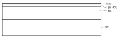
도 2를 참조하면, 성장 기판(101) 상에 상기 발광 구조층(135)을 형성한다.Referring to FIG. 2, the light emitting
상기 성장기판(101)은 예를 들어, 사파이어(Al2O3), SiC, GaAs, GaN, ZnO, Si, GaP, InP, Ge 중 적어도 하나로 형성될 수 있으며, 이에 대해 한정하지는 않는다.The
상기 발광 구조층(135)은 상기 성장기판(101) 상에 상기 제1 도전형의 반도체층(110), 활성층(120) 및 제2 도전형의 반도체층(130)을 순차적으로 성장함으로써 형성될 수 있다.The light emitting
상기 발광 구조층(135)은 예를 들어, 유기금속 화학 증착법(MOCVD; Metal Organic Chemical Vapor Deposition), 화학 증착법(CVD; Chemical Vapor Deposition), 플라즈마 화학 증착법(PECVD; Plasma-Enhanced Chemical Vapor Deposition), 분자선 성장법(MBE; Molecular Beam Epitaxy), 수소화물 기상 성장법(HVPE; Hydride Vapor Phase Epitaxy) 등의 방법을 이용하여 형성될 수 있으며, 이에 대해 한정하지는 않는다.The light emitting
한편, 상기 발광 구조층(135) 및 상기 성장 기판(101) 사이에는 격자 상수 차이를 완화하기 위해 버퍼층(미도시) 및/또는 언도프트 질화물층(미도시)이 형성될 수도 있다Meanwhile, a buffer layer and / or an undoped nitride layer (not shown) may be formed between the light emitting
도 3을 참조하면, 상기 발광 구조층(135) 상에 단위 칩 영역에 대응하여 상기 전도성 보호층(140)이 형성된다.Referring to FIG. 3, the
상기 전도성 보호층(140)은 마스크 패턴을 이용하여 단위 칩 영역의 둘레에 형성될 수 있다. 상기 전도성 보호층(140)은 다양한 증착 방법을 이용하여 형성할 수 있다.The conductive
특히, 상기 전도성 보호층(140)이 Ti, Ni, Pt, Pd, Rh, Ir, W 중 적어도 어느 하나로 형성되는 경우, 상기 전도성 보호층(140)을 스퍼터링(sputtering) 방법을 이용하면 고밀도로 형성이 가능하기 때문에 아이솔레이션 에칭시 깨지거나 파편이 발생되지 않는다.In particular, when the conductive
도 4를 참조하면, 상기 제2 도전형의 반도체층(130) 상에 상기 전류 차단층(145)을 형성할 수 있다. 상기 전류 차단층(145)은 마스크 패턴을 이용하여 형성될 수 있다.Referring to FIG. 4, the
예를 들어, 상기 제2 도전형의 반도체층(130) 상에 SiO2층을 형성한 후, 마스크 패턴을 이용하여 상기 전류 차단층(145)을 형성할 수 있다.For example, after forming the SiO 2 layer on the second
도 5 및 도 6을 참조하면, 상기 제2 도전형의 반도체층(130) 및 상기 전류차단층(145) 상에 상기 오믹 접촉층(150)을 형성하고, 상기 오믹 접촉층(150) 상에 상기 반사층(160)을 형성할 수 있다.5 and 6, the
상기 오믹 접촉층(150)은 상기 전도성 보호층(140)과 동일한 물질로 형성될 수 있으며, 이 경우 상기 제2 도전형의 반도체층(130) 상에 상기 전류 차단층(145)을 형성한 후, 상기 전도성 보호층(140)과 오믹 접촉층(150)을 동시에 형성할 수도 있다.The
상기 오믹 접촉층(150) 및 상기 반사층(160)은 예를 들어, 전자빔(E-beam) 증착, 스퍼터링(Sputtering), PECVD(Plasma Enhanced Chemical Vapor Deposition) 중 어느 하나의 방법에 의해 형성될 수 있다. The
상기 오믹 접촉층(150)과 반사층(160)이 형성되는 면적은 다양하게 선택될 수 있으며, 상기 오믹 접촉층(150) 및/또는 반사층(160)이 형성되는 면적에 따라 도 11 및 도 12에서 설명한 다른 실시예들의 발광 소자가 제작될 수 있다.The area in which the
도 7을 참조하면, 상기 반사층(160) 및 상기 전도성 보호층(140) 상에 상기 접합층(170)을 형성하고, 상기 접합층(170) 상에 상기 전도성 지지기판(175)을 형성한다.Referring to FIG. 7, the
상기 접합층(170)은 상기 반사층(160), 상기 오믹 접촉층(150)의 단부 및 상기 전도성 보호층(140)에 접촉되어, 상기 반사층(160), 오믹 접촉층(150), 및 전도성 보호층(140) 사이의 접착력을 강화시켜 줄 수 있다.The
상기 전도성 지지기판(175)은 상기 접합층(170) 상에 부착된다. 비록, 실시예에서는 상기 전도성 지지기판(175)이 상기 접합층(170)을 통해 본딩 방식으로 결합된 것이 예시되어 있으나, 상기 전도성 지지기판(175)을 도금 방식 또는 증착 방식으로 형성하는 것도 가능하다.The
도 8을 참조하면, 상기 성장기판(101)을 상기 발광 구조층(135)으로부터 제거한다. 도 8에서는 도 7에 도시된 구조물을 뒤집어서 도시하였다. Referring to FIG. 8, the
상기 성장기판(101)은 레이저 리프트 오프(Laser Lift Off) 방법 또는 화학적 리프트 오프(Chemical Lift Off) 방법에 의해 제거될 수 있다.The
도 9를 참조하면, 상기 발광 구조층(135)에 단위 칩 영역에 따라 아이솔레이션(isolation) 에칭을 실시하여 복수개의 발광 구조층(135)으로 분리한다.Referring to FIG. 9, an isolation etching is performed on the light emitting
예를 들어, 상기 아이솔레이션 에칭은 ICP(Inductively Coupled Plasma)와 같은 건식 식각 방법에 의해 실시될 수 있다.For example, the isolation etching may be performed by a dry etching method such as inductively coupled plasma (ICP).
도 10을 참조하면, 상기 전도성 보호층(140) 및 발광 구조층(135) 상에 패시베이션층(180)을 형성하고, 상기 제1 도전형의 반도체층(110)의 상면이 노출되도록 상기 패시베이션층(180)을 선택적으로 제거한다. Referring to FIG. 10, a
그리고, 상기 제1 도전형의 반도체층(110)의 상면에 광 추출 효율 향상을 위한 러프니스 패턴(112)을 형성하고, 상기 러프니스 패턴(112) 상에 전극(115)을 형성한다. 상기 러프니스 패턴(112)은 습식 식각 공정 또는 건식 식각 공정에 의해 형성될 수 있다.A
그리고, 상기 구조물을 칩 분리 공정을 통해 단위 칩 영역으로 분리하면 복수개의 발광 소자를 제작할 수 있다.In addition, when the structure is separated into a unit chip region through a chip separation process, a plurality of light emitting devices may be manufactured.
상기 칩 분리 공정은 예를 들어, 블레이드(blade)를 이용해 물리적인 힘을 가하여 분리시키는 브레이킹 공정, 칩 경계에 레이저를 조사하여 칩을 분리시키는 레이저 스크라이빙 공정, 습식 식각 또는 건식 식각을 포함하는 식각 공정 등을 포함할 수 있으나, 이에 대해 한정하지는 않는다.The chip separation process may include, for example, a braking process of separating a chip by applying a physical force using a blade, a laser scribing process of separating a chip by irradiating a laser to a chip boundary, and a wet etching or a dry etching process. It may include an etching process, but is not limited thereto.
도 14는 실시예에 따른 발광 소자를 포함하는 발광 소자 패키지의 단면도이다. 14 is a cross-sectional view of a light emitting device package including a light emitting device according to the embodiment.
도 14를 참조하면, 실시예에 따른 발광 소자 패키지는 패키지 몸체(10)와, 상기 패키지 몸체(10)에 설치된 제1 전극층(31) 및 제2 전극층(32)과, 상기 패키지 몸체(10)에 설치되어 상기 제1 전극층(31) 및 제2 전극층(32)과 전기적으로 연결되는 발광 소자(100)와, 상기 발광 소자(100)를 포위하는 몰딩부재(40)를 포함한다.Referring to FIG. 14, the light emitting device package according to the embodiment may include a
상기 패키지 몸체(10)는 실리콘 재질, 합성수지 재질, 또는 금속 재질을 포함하여 형성될 수 있으며, 측면이 경사면으로 형성된 캐비티를 가질 수 있다.The
상기 제1 전극층(31) 및 제2 전극층(32)은 서로 전기적으로 분리되며, 상기 발광 소자(100)에 전원을 제공한다. 또한, 상기 제1 전극층(31) 및 제2 전극층(32)은 상기 발광 소자(100)에서 발생된 빛을 반사시켜 광 효율을 증가시킬 수 있으며, 상기 발광 소자(100)에서 발생된 열을 외부로 배출시키는 역할을 할 수도 있다.The
상기 발광 소자(100)는 상기 패키지 몸체(10) 상에 설치되거나 상기 제1 전극층(31) 또는 제2 전극층(32) 상에 설치될 수 있다.The
상기 발광 소자(100)는 상기 제1 전극층(31) 및 제2 전극층(32)과 와이어 방식, 플립칩 방식 또는 다이 본딩 방식 중 어느 하나에 의해 전기적으로 연결될 수도 있다. 실시예에서는 상기 발광 소자(100)가 상기 제1 전극층(31)과 와이어(50)를 통해 전기적으로 연결되고 상기 제2 전극층(32)과 직접 접촉하여 전기적으로 연결된 것이 예시되어 있다.The
상기 몰딩부재(40)는 상기 발광 소자(100)를 포위하여 상기 발광 소자(100)를 보호할 수 있다. 또한, 상기 몰딩부재(40)에는 형광체가 포함되어 상기 발광 소자(100)에서 방출된 광의 파장을 변화시킬 수 있다.The
이상에서 실시예들에 설명된 특징, 구조, 효과 등은 본 발명의 적어도 하나의 실시예에 포함되며, 반드시 하나의 실시예에만 한정되는 것은 아니다. 나아가, 각 실시예에서 예시된 특징, 구조, 효과 등은 실시예들이 속하는 분야의 통상의 지식을 가지는 자에 의해 다른 실시예들에 대해서도 조합 또는 변형되어 실시 가능하 다. 따라서 이러한 조합과 변형에 관계된 내용들은 본 발명의 범위에 포함되는 것으로 해석되어야 할 것이다.Features, structures, effects, and the like described in the above embodiments are included in at least one embodiment of the present invention, and are not necessarily limited to only one embodiment. Furthermore, the features, structures, effects, and the like illustrated in the embodiments may be combined or modified with respect to other embodiments by those skilled in the art to which the embodiments belong. Therefore, it should be understood that the present invention is not limited to these combinations and modifications.
또한, 이상에서 실시예를 중심으로 설명하였으나 이는 단지 예시일 뿐 본 발명을 한정하는 것이 아니며, 본 발명이 속하는 분야의 통상의 지식을 가진 자라면 본 실시예의 본질적인 특성을 벗어나지 않는 범위에서 이상에 예시되지 않은 여러 가지의 변형과 응용이 가능함을 알 수 있을 것이다. 예를 들어, 실시예에 구체적으로 나타난 각 구성 요소는 변형하여 실시할 수 있는 것이다. 그리고 이러한 변형과 응용에 관계된 차이점들은 첨부된 청구 범위에서 규정하는 본 발명의 범위에 포함되는 것으로 해석되어야 할 것이다.In addition, the above description has been made with reference to the embodiment, which is merely an example, and is not intended to limit the present invention. Those skilled in the art to which the present invention pertains will be illustrated as above without departing from the essential characteristics of the present embodiment. It will be appreciated that various modifications and applications are possible. For example, each component specifically shown in the embodiment can be modified. And differences relating to such modifications and applications will have to be construed as being included in the scope of the invention defined in the appended claims.
도 1은 제1 실시예에 따른 발광 소자를 설명하는 도면.1 is a view for explaining a light emitting element according to the first embodiment;
도 2 내지 도 10은 실시예에 따른 발광 소자의 제조방법을 설명하는 도면2 to 10 illustrate a method of manufacturing a light emitting device according to an embodiment.
도 11은 제2 실시예에 따른 발광 소자를 설명하는 도면.11 is a view for explaining a light emitting element according to the second embodiment.
도 12는 제3 실시예에 따른 발광 소자를 설명하는 도면.12 is a view for explaining a light emitting element according to the third embodiment.
도 13은 실시예에 따른 발광 소자에서 전극의 평면 상의 형태를 도시한 도면.13 is a view showing a shape on a plane of the electrode in the light emitting device according to the embodiment.
도 14는 실시예에 따른 발광 소자를 포함하는 발광 소자 패키지의 단면도.14 is a cross-sectional view of a light emitting device package including a light emitting device according to the embodiment.
Claims (20)
Priority Applications (13)
| Application Number | Priority Date | Filing Date | Title |
|---|---|---|---|
| KR1020090121740A KR100986374B1 (en) | 2009-12-09 | 2009-12-09 | Light emitting device, method for fabricating the light emitting device and light emitting device package |
| EP15171500.0A EP2942823B1 (en) | 2009-12-09 | 2010-12-07 | Light emitting device, light emitting package, and lighting system |
| EP10194055.9A EP2333852B1 (en) | 2009-12-09 | 2010-12-07 | Light emitting device and light emitting package |
| EP13174920.2A EP2660883B1 (en) | 2009-12-09 | 2010-12-07 | Light emitting device, light emitting device manufacturing method, light emitting package, and lighting system |
| CN201410469501.4A CN104241485B (en) | 2009-12-09 | 2010-12-09 | Luminescent device, manufacturing method of lighting device, light emitting device package and lighting system |
| CN201310276526.8A CN103400920B (en) | 2009-12-09 | 2010-12-09 | Light emitting device, light emitting device manufacturing method, light emitting package, and lighting system |
| CN201410468589.8A CN104241484B (en) | 2009-12-09 | 2010-12-09 | Luminescent device and light emitting device packaging piece |
| CN201010591857.7A CN102097569B (en) | 2009-12-09 | 2010-12-09 | Light emitting device, light emitting device manufacturing method, light emitting package, and lighting system |
| US12/964,161 US8610157B2 (en) | 2009-12-09 | 2010-12-09 | Light emitting apparatus |
| US14/049,006 US9911908B2 (en) | 2009-12-09 | 2013-10-08 | Light emitting apparatus |
| US14/447,397 US9281448B2 (en) | 2009-12-09 | 2014-07-30 | Light emitting apparatus |
| US14/789,808 US9899581B2 (en) | 2009-12-09 | 2015-07-01 | Light emitting apparatus |
| US15/877,998 US11335838B2 (en) | 2009-12-09 | 2018-01-23 | Light emitting apparatus |
Applications Claiming Priority (1)
| Application Number | Priority Date | Filing Date | Title |
|---|---|---|---|
| KR1020090121740A KR100986374B1 (en) | 2009-12-09 | 2009-12-09 | Light emitting device, method for fabricating the light emitting device and light emitting device package |
Publications (1)
| Publication Number | Publication Date |
|---|---|
| KR100986374B1 true KR100986374B1 (en) | 2010-10-08 |
Family
ID=43135187
Family Applications (1)
| Application Number | Title | Priority Date | Filing Date |
|---|---|---|---|
| KR1020090121740A KR100986374B1 (en) | 2009-12-09 | 2009-12-09 | Light emitting device, method for fabricating the light emitting device and light emitting device package |
Country Status (1)
| Country | Link |
|---|---|
| KR (1) | KR100986374B1 (en) |
Cited By (11)
| Publication number | Priority date | Publication date | Assignee | Title |
|---|---|---|---|---|
| KR101063907B1 (en) | 2010-10-25 | 2011-09-08 | 엘지이노텍 주식회사 | A light emitting device |
| WO2011145850A2 (en) * | 2010-05-18 | 2011-11-24 | Seoul Opto Device Co., Ltd. | High efficiency light emitting diode and method of fabricating the same |
| KR20120040125A (en) * | 2011-12-09 | 2012-04-26 | 서울옵토디바이스주식회사 | High efficiency light emitting diode and method of fabricating the same |
| KR101154511B1 (en) * | 2010-10-18 | 2012-06-13 | 서울옵토디바이스주식회사 | High efficiency light emitting diode and method of fabricating the same |
| KR20130046755A (en) * | 2011-10-28 | 2013-05-08 | 엘지이노텍 주식회사 | Light emitting device |
| US8552452B2 (en) | 2010-10-11 | 2013-10-08 | Lg Innotek Co., Ltd. | Light emitting device and lighting instrument including the same |
| KR20140012466A (en) * | 2012-07-20 | 2014-02-03 | 엘지이노텍 주식회사 | Light emitting device, light emitting device package, and light unit |
| KR20150107245A (en) * | 2014-03-13 | 2015-09-23 | 엘지이노텍 주식회사 | Light emitting device |
| KR101742619B1 (en) | 2011-01-26 | 2017-06-01 | 엘지이노텍 주식회사 | Light emitting diode and method for fabricating the light emitting device |
| KR101795026B1 (en) * | 2011-01-27 | 2017-11-07 | 엘지이노텍 주식회사 | Light emitting device |
| KR101826979B1 (en) | 2011-06-23 | 2018-02-07 | 엘지이노텍 주식회사 | Light emitting device and light emitting device package |
Citations (4)
| Publication number | Priority date | Publication date | Assignee | Title |
|---|---|---|---|---|
| KR20070087502A (en) * | 2006-02-23 | 2007-08-28 | 아리마 옵토일렉트로닉스 코포레이션 | Light emitting diode by use of metal diffusion bonding technology and method of producing such light emitting diode |
| KR100872717B1 (en) * | 2007-06-22 | 2008-12-05 | 엘지이노텍 주식회사 | Light emitting device and manufacturing method thereof |
| KR100909733B1 (en) | 2002-01-28 | 2009-07-29 | 니치아 카가쿠 고교 가부시키가이샤 | Nitride semiconductor device having support substrate and manufacturing method thereof |
| KR20090116840A (en) * | 2008-05-08 | 2009-11-12 | 엘지이노텍 주식회사 | Light emitting device and method for fabricating the same |
-
2009
- 2009-12-09 KR KR1020090121740A patent/KR100986374B1/en active IP Right Grant
Patent Citations (4)
| Publication number | Priority date | Publication date | Assignee | Title |
|---|---|---|---|---|
| KR100909733B1 (en) | 2002-01-28 | 2009-07-29 | 니치아 카가쿠 고교 가부시키가이샤 | Nitride semiconductor device having support substrate and manufacturing method thereof |
| KR20070087502A (en) * | 2006-02-23 | 2007-08-28 | 아리마 옵토일렉트로닉스 코포레이션 | Light emitting diode by use of metal diffusion bonding technology and method of producing such light emitting diode |
| KR100872717B1 (en) * | 2007-06-22 | 2008-12-05 | 엘지이노텍 주식회사 | Light emitting device and manufacturing method thereof |
| KR20090116840A (en) * | 2008-05-08 | 2009-11-12 | 엘지이노텍 주식회사 | Light emitting device and method for fabricating the same |
Cited By (17)
| Publication number | Priority date | Publication date | Assignee | Title |
|---|---|---|---|---|
| WO2011145850A2 (en) * | 2010-05-18 | 2011-11-24 | Seoul Opto Device Co., Ltd. | High efficiency light emitting diode and method of fabricating the same |
| WO2011145850A3 (en) * | 2010-05-18 | 2012-02-23 | Seoul Opto Device Co., Ltd. | High efficiency light emitting diode and method of fabricating the same |
| US8552452B2 (en) | 2010-10-11 | 2013-10-08 | Lg Innotek Co., Ltd. | Light emitting device and lighting instrument including the same |
| EP2439793A3 (en) * | 2010-10-11 | 2014-07-09 | LG Innotek Co., Ltd. | Light emitting device and lighting instrument including the same |
| KR101154511B1 (en) * | 2010-10-18 | 2012-06-13 | 서울옵토디바이스주식회사 | High efficiency light emitting diode and method of fabricating the same |
| KR101063907B1 (en) | 2010-10-25 | 2011-09-08 | 엘지이노텍 주식회사 | A light emitting device |
| KR101742619B1 (en) | 2011-01-26 | 2017-06-01 | 엘지이노텍 주식회사 | Light emitting diode and method for fabricating the light emitting device |
| KR101795026B1 (en) * | 2011-01-27 | 2017-11-07 | 엘지이노텍 주식회사 | Light emitting device |
| KR101826979B1 (en) | 2011-06-23 | 2018-02-07 | 엘지이노텍 주식회사 | Light emitting device and light emitting device package |
| KR20130046755A (en) * | 2011-10-28 | 2013-05-08 | 엘지이노텍 주식회사 | Light emitting device |
| KR101871372B1 (en) * | 2011-10-28 | 2018-08-02 | 엘지이노텍 주식회사 | Light emitting device |
| KR20120040125A (en) * | 2011-12-09 | 2012-04-26 | 서울옵토디바이스주식회사 | High efficiency light emitting diode and method of fabricating the same |
| KR101634370B1 (en) * | 2011-12-09 | 2016-06-28 | 서울바이오시스 주식회사 | High efficiency light emitting diode and method of fabricating the same |
| KR20140012466A (en) * | 2012-07-20 | 2014-02-03 | 엘지이노텍 주식회사 | Light emitting device, light emitting device package, and light unit |
| KR101946918B1 (en) * | 2012-07-20 | 2019-02-12 | 엘지이노텍 주식회사 | Light emitting device, light emitting device package, and light unit |
| KR20150107245A (en) * | 2014-03-13 | 2015-09-23 | 엘지이노텍 주식회사 | Light emitting device |
| KR102142716B1 (en) * | 2014-03-13 | 2020-08-07 | 엘지이노텍 주식회사 | Light emitting device |
Similar Documents
| Publication | Publication Date | Title |
|---|---|---|
| KR100986353B1 (en) | Light emitting device, method for fabricating the light emitting device and light emitting device package | |
| KR101020963B1 (en) | Light emitting device, method for fabricating the light emitting device and light emitting device package | |
| KR101014155B1 (en) | Light emitting device, method for fabricating the light emitting device and light emitting device package | |
| KR100974787B1 (en) | Light emitting device, method for fabricating the light emitting device and light emitting device package | |
| KR100986374B1 (en) | Light emitting device, method for fabricating the light emitting device and light emitting device package | |
| EP2518782B1 (en) | Light emitting device and light emitting device package | |
| JP5650446B2 (en) | Semiconductor light emitting device | |
| US8168993B2 (en) | Light emtting device, method for manufacturing light emitting device, and light emitting apparatus | |
| KR101039999B1 (en) | Semiconductor light emitting device and fabrication method thereof | |
| KR101014071B1 (en) | Light emitting device, method for fabricating the light emitting device, light emitting device package and lighting system | |
| KR101014013B1 (en) | Semiconductor light emitting device and fabrication method thereof | |
| JP5816243B2 (en) | Light emitting device and light emitting device package | |
| KR20130120615A (en) | Light emitting device and light emitting device package | |
| KR20110103608A (en) | Light emitting device, method for fabricating the light emitting device and light emitting device package | |
| KR100986523B1 (en) | Semiconductor light emitting device and fabrication method thereof | |
| KR101034144B1 (en) | Light emitting device, method for fabricating the light emitting device, light emitting device package and lighting system | |
| KR100999701B1 (en) | Light emitting device, method for fabricating the light emitting device and light emitting device package | |
| KR102353570B1 (en) | Light emitting device and light emitting device package having thereof | |
| KR102250516B1 (en) | Light emitting device | |
| KR102164087B1 (en) | Light emitting deviceand light emitting device package thereof | |
| KR20120014972A (en) | Light emitting device, method for fabricating the light emitting device, light emitting device package and lighting system | |
| KR20110118333A (en) | Light emitting device, method for fabricating the light emitting device, light emitting device package and lighting system | |
| KR20120037100A (en) | A light emitting device and a light emitting device package | |
| KR101750207B1 (en) | Light emitting device and light emitting device package | |
| KR101643410B1 (en) | Light emitting device, method for fabricating the light emitting device and light emitting device package |
Legal Events
| Date | Code | Title | Description |
|---|---|---|---|
| A201 | Request for examination | ||
| A302 | Request for accelerated examination | ||
| E902 | Notification of reason for refusal | ||
| E701 | Decision to grant or registration of patent right | ||
| GRNT | Written decision to grant | ||
| FPAY | Annual fee payment |
Payment date: 20130905 Year of fee payment: 4 |
|
| FPAY | Annual fee payment |
Payment date: 20150904 Year of fee payment: 6 |
|
| FPAY | Annual fee payment |
Payment date: 20160905 Year of fee payment: 7 |
|
| FPAY | Annual fee payment |
Payment date: 20170905 Year of fee payment: 8 |
|
| FPAY | Annual fee payment |
Payment date: 20180910 Year of fee payment: 9 |
|
| FPAY | Annual fee payment |
Payment date: 20190916 Year of fee payment: 10 |