KR100811040B1 - Ferroelectric film manufacturing apparatus - Google Patents
Ferroelectric film manufacturing apparatus Download PDFInfo
- Publication number
- KR100811040B1 KR100811040B1 KR1020077008442A KR20077008442A KR100811040B1 KR 100811040 B1 KR100811040 B1 KR 100811040B1 KR 1020077008442 A KR1020077008442 A KR 1020077008442A KR 20077008442 A KR20077008442 A KR 20077008442A KR 100811040 B1 KR100811040 B1 KR 100811040B1
- Authority
- KR
- South Korea
- Prior art keywords
- ferroelectric film
- film
- target
- ferroelectric
- electric field
- Prior art date
Links
- 238000004519 manufacturing process Methods 0.000 title claims abstract description 31
- 238000012545 processing Methods 0.000 claims abstract description 84
- 239000000463 material Substances 0.000 claims abstract description 38
- 238000010438 heat treatment Methods 0.000 claims abstract description 15
- 239000000470 constituent Substances 0.000 claims abstract description 9
- 238000000151 deposition Methods 0.000 claims abstract description 4
- 230000005684 electric field Effects 0.000 claims description 49
- 229910052758 niobium Inorganic materials 0.000 claims description 16
- 229910052715 tantalum Inorganic materials 0.000 claims description 16
- 229910052712 strontium Inorganic materials 0.000 claims description 13
- 230000001681 protective effect Effects 0.000 claims description 7
- 150000002500 ions Chemical class 0.000 claims description 6
- 239000000758 substrate Substances 0.000 claims description 6
- VYPSYNLAJGMNEJ-UHFFFAOYSA-N silicon dioxide Inorganic materials O=[Si]=O VYPSYNLAJGMNEJ-UHFFFAOYSA-N 0.000 claims description 4
- 230000002093 peripheral effect Effects 0.000 claims description 3
- 239000010453 quartz Substances 0.000 claims description 3
- 239000011248 coating agent Substances 0.000 claims description 2
- 238000000576 coating method Methods 0.000 claims description 2
- 230000007423 decrease Effects 0.000 claims description 2
- 230000001590 oxidative effect Effects 0.000 abstract description 6
- 239000010408 film Substances 0.000 description 272
- 239000001301 oxygen Substances 0.000 description 60
- 229910052760 oxygen Inorganic materials 0.000 description 60
- 239000007789 gas Substances 0.000 description 55
- QVGXLLKOCUKJST-UHFFFAOYSA-N atomic oxygen Chemical compound [O] QVGXLLKOCUKJST-UHFFFAOYSA-N 0.000 description 40
- 238000000034 method Methods 0.000 description 37
- 239000004020 conductor Substances 0.000 description 34
- XKRFYHLGVUSROY-UHFFFAOYSA-N Argon Chemical compound [Ar] XKRFYHLGVUSROY-UHFFFAOYSA-N 0.000 description 26
- 238000004544 sputter deposition Methods 0.000 description 24
- 238000000137 annealing Methods 0.000 description 22
- 239000004065 semiconductor Substances 0.000 description 18
- 229910052786 argon Inorganic materials 0.000 description 17
- 230000015654 memory Effects 0.000 description 17
- 238000009832 plasma treatment Methods 0.000 description 13
- MYMOFIZGZYHOMD-UHFFFAOYSA-N Dioxygen Chemical compound O=O MYMOFIZGZYHOMD-UHFFFAOYSA-N 0.000 description 10
- 229910001882 dioxygen Inorganic materials 0.000 description 10
- 230000010287 polarization Effects 0.000 description 10
- 239000003990 capacitor Substances 0.000 description 9
- -1 argon ions Chemical class 0.000 description 8
- 229910052743 krypton Inorganic materials 0.000 description 7
- DNNSSWSSYDEUBZ-UHFFFAOYSA-N krypton atom Chemical group [Kr] DNNSSWSSYDEUBZ-UHFFFAOYSA-N 0.000 description 7
- 230000003647 oxidation Effects 0.000 description 5
- 238000007254 oxidation reaction Methods 0.000 description 5
- 238000011084 recovery Methods 0.000 description 5
- 230000005669 field effect Effects 0.000 description 4
- 239000012535 impurity Substances 0.000 description 4
- WABPQHHGFIMREM-UHFFFAOYSA-N lead(0) Chemical compound [Pb] WABPQHHGFIMREM-UHFFFAOYSA-N 0.000 description 4
- 238000003980 solgel method Methods 0.000 description 4
- XUIMIQQOPSSXEZ-UHFFFAOYSA-N Silicon Chemical compound [Si] XUIMIQQOPSSXEZ-UHFFFAOYSA-N 0.000 description 3
- 229910044991 metal oxide Inorganic materials 0.000 description 3
- 150000004706 metal oxides Chemical class 0.000 description 3
- 229910052710 silicon Inorganic materials 0.000 description 3
- 239000010703 silicon Substances 0.000 description 3
- 238000012795 verification Methods 0.000 description 3
- 230000004888 barrier function Effects 0.000 description 2
- 230000015572 biosynthetic process Effects 0.000 description 2
- 238000009529 body temperature measurement Methods 0.000 description 2
- 238000002425 crystallisation Methods 0.000 description 2
- 230000008025 crystallization Effects 0.000 description 2
- 238000009792 diffusion process Methods 0.000 description 2
- BASFCYQUMIYNBI-UHFFFAOYSA-N platinum Chemical compound [Pt] BASFCYQUMIYNBI-UHFFFAOYSA-N 0.000 description 2
- 239000002243 precursor Substances 0.000 description 2
- 239000010409 thin film Substances 0.000 description 2
- 229910000838 Al alloy Inorganic materials 0.000 description 1
- IJGRMHOSHXDMSA-UHFFFAOYSA-N Atomic nitrogen Chemical compound N#N IJGRMHOSHXDMSA-UHFFFAOYSA-N 0.000 description 1
- 238000005229 chemical vapour deposition Methods 0.000 description 1
- 238000001816 cooling Methods 0.000 description 1
- 230000003247 decreasing effect Effects 0.000 description 1
- 238000012217 deletion Methods 0.000 description 1
- 230000037430 deletion Effects 0.000 description 1
- 230000008021 deposition Effects 0.000 description 1
- 238000011161 development Methods 0.000 description 1
- 229910001873 dinitrogen Inorganic materials 0.000 description 1
- 230000001747 exhibiting effect Effects 0.000 description 1
- 238000002474 experimental method Methods 0.000 description 1
- 230000005621 ferroelectricity Effects 0.000 description 1
- 230000006870 function Effects 0.000 description 1
- 238000010348 incorporation Methods 0.000 description 1
- 239000000203 mixture Substances 0.000 description 1
- 230000036961 partial effect Effects 0.000 description 1
- 238000000206 photolithography Methods 0.000 description 1
- 229910052697 platinum Inorganic materials 0.000 description 1
- 230000000644 propagated effect Effects 0.000 description 1
- 230000005855 radiation Effects 0.000 description 1
- 230000002829 reductive effect Effects 0.000 description 1
- 239000003566 sealing material Substances 0.000 description 1
- LIVNPJMFVYWSIS-UHFFFAOYSA-N silicon monoxide Chemical compound [Si-]#[O+] LIVNPJMFVYWSIS-UHFFFAOYSA-N 0.000 description 1
- 230000002269 spontaneous effect Effects 0.000 description 1
- 230000003068 static effect Effects 0.000 description 1
- 238000003860 storage Methods 0.000 description 1
- 239000000126 substance Substances 0.000 description 1
- 230000001502 supplementing effect Effects 0.000 description 1
- 229910052724 xenon Inorganic materials 0.000 description 1
- FHNFHKCVQCLJFQ-UHFFFAOYSA-N xenon atom Chemical compound [Xe] FHNFHKCVQCLJFQ-UHFFFAOYSA-N 0.000 description 1
Images


Classifications
-
- H01L27/105—
-
- C—CHEMISTRY; METALLURGY
- C01—INORGANIC CHEMISTRY
- C01G—COMPOUNDS CONTAINING METALS NOT COVERED BY SUBCLASSES C01D OR C01F
- C01G35/00—Compounds of tantalum
-
- C—CHEMISTRY; METALLURGY
- C01—INORGANIC CHEMISTRY
- C01G—COMPOUNDS CONTAINING METALS NOT COVERED BY SUBCLASSES C01D OR C01F
- C01G35/00—Compounds of tantalum
- C01G35/006—Compounds containing tantalum, with or without oxygen or hydrogen, and containing two or more other elements
-
- C—CHEMISTRY; METALLURGY
- C23—COATING METALLIC MATERIAL; COATING MATERIAL WITH METALLIC MATERIAL; CHEMICAL SURFACE TREATMENT; DIFFUSION TREATMENT OF METALLIC MATERIAL; COATING BY VACUUM EVAPORATION, BY SPUTTERING, BY ION IMPLANTATION OR BY CHEMICAL VAPOUR DEPOSITION, IN GENERAL; INHIBITING CORROSION OF METALLIC MATERIAL OR INCRUSTATION IN GENERAL
- C23C—COATING METALLIC MATERIAL; COATING MATERIAL WITH METALLIC MATERIAL; SURFACE TREATMENT OF METALLIC MATERIAL BY DIFFUSION INTO THE SURFACE, BY CHEMICAL CONVERSION OR SUBSTITUTION; COATING BY VACUUM EVAPORATION, BY SPUTTERING, BY ION IMPLANTATION OR BY CHEMICAL VAPOUR DEPOSITION, IN GENERAL
- C23C14/00—Coating by vacuum evaporation, by sputtering or by ion implantation of the coating forming material
- C23C14/06—Coating by vacuum evaporation, by sputtering or by ion implantation of the coating forming material characterised by the coating material
- C23C14/08—Oxides
- C23C14/088—Oxides of the type ABO3 with A representing alkali, alkaline earth metal or Pb and B representing a refractory or rare earth metal
-
- H—ELECTRICITY
- H01—ELECTRIC ELEMENTS
- H01B—CABLES; CONDUCTORS; INSULATORS; SELECTION OF MATERIALS FOR THEIR CONDUCTIVE, INSULATING OR DIELECTRIC PROPERTIES
- H01B3/00—Insulators or insulating bodies characterised by the insulating materials; Selection of materials for their insulating or dielectric properties
- H01B3/02—Insulators or insulating bodies characterised by the insulating materials; Selection of materials for their insulating or dielectric properties mainly consisting of inorganic substances
- H01B3/12—Insulators or insulating bodies characterised by the insulating materials; Selection of materials for their insulating or dielectric properties mainly consisting of inorganic substances ceramics
-
- H—ELECTRICITY
- H01—ELECTRIC ELEMENTS
- H01L—SEMICONDUCTOR DEVICES NOT COVERED BY CLASS H10
- H01L21/00—Processes or apparatus adapted for the manufacture or treatment of semiconductor or solid state devices or of parts thereof
- H01L21/02—Manufacture or treatment of semiconductor devices or of parts thereof
- H01L21/02104—Forming layers
- H01L21/02107—Forming insulating materials on a substrate
- H01L21/02109—Forming insulating materials on a substrate characterised by the type of layer, e.g. type of material, porous/non-porous, pre-cursors, mixtures or laminates
- H01L21/02112—Forming insulating materials on a substrate characterised by the type of layer, e.g. type of material, porous/non-porous, pre-cursors, mixtures or laminates characterised by the material of the layer
- H01L21/02172—Forming insulating materials on a substrate characterised by the type of layer, e.g. type of material, porous/non-porous, pre-cursors, mixtures or laminates characterised by the material of the layer the material containing at least one metal element, e.g. metal oxides, metal nitrides, metal oxynitrides or metal carbides
- H01L21/02175—Forming insulating materials on a substrate characterised by the type of layer, e.g. type of material, porous/non-porous, pre-cursors, mixtures or laminates characterised by the material of the layer the material containing at least one metal element, e.g. metal oxides, metal nitrides, metal oxynitrides or metal carbides characterised by the metal
- H01L21/02183—Forming insulating materials on a substrate characterised by the type of layer, e.g. type of material, porous/non-porous, pre-cursors, mixtures or laminates characterised by the material of the layer the material containing at least one metal element, e.g. metal oxides, metal nitrides, metal oxynitrides or metal carbides characterised by the metal the material containing tantalum, e.g. Ta2O5
-
- H—ELECTRICITY
- H01—ELECTRIC ELEMENTS
- H01L—SEMICONDUCTOR DEVICES NOT COVERED BY CLASS H10
- H01L21/00—Processes or apparatus adapted for the manufacture or treatment of semiconductor or solid state devices or of parts thereof
- H01L21/02—Manufacture or treatment of semiconductor devices or of parts thereof
- H01L21/02104—Forming layers
- H01L21/02107—Forming insulating materials on a substrate
- H01L21/02109—Forming insulating materials on a substrate characterised by the type of layer, e.g. type of material, porous/non-porous, pre-cursors, mixtures or laminates
- H01L21/02112—Forming insulating materials on a substrate characterised by the type of layer, e.g. type of material, porous/non-porous, pre-cursors, mixtures or laminates characterised by the material of the layer
- H01L21/02172—Forming insulating materials on a substrate characterised by the type of layer, e.g. type of material, porous/non-porous, pre-cursors, mixtures or laminates characterised by the material of the layer the material containing at least one metal element, e.g. metal oxides, metal nitrides, metal oxynitrides or metal carbides
- H01L21/02175—Forming insulating materials on a substrate characterised by the type of layer, e.g. type of material, porous/non-porous, pre-cursors, mixtures or laminates characterised by the material of the layer the material containing at least one metal element, e.g. metal oxides, metal nitrides, metal oxynitrides or metal carbides characterised by the metal
- H01L21/02194—Forming insulating materials on a substrate characterised by the type of layer, e.g. type of material, porous/non-porous, pre-cursors, mixtures or laminates characterised by the material of the layer the material containing at least one metal element, e.g. metal oxides, metal nitrides, metal oxynitrides or metal carbides characterised by the metal the material containing more than one metal element
-
- H—ELECTRICITY
- H01—ELECTRIC ELEMENTS
- H01L—SEMICONDUCTOR DEVICES NOT COVERED BY CLASS H10
- H01L21/00—Processes or apparatus adapted for the manufacture or treatment of semiconductor or solid state devices or of parts thereof
- H01L21/02—Manufacture or treatment of semiconductor devices or of parts thereof
- H01L21/02104—Forming layers
- H01L21/02107—Forming insulating materials on a substrate
- H01L21/02109—Forming insulating materials on a substrate characterised by the type of layer, e.g. type of material, porous/non-porous, pre-cursors, mixtures or laminates
- H01L21/022—Forming insulating materials on a substrate characterised by the type of layer, e.g. type of material, porous/non-porous, pre-cursors, mixtures or laminates the layer being a laminate, i.e. composed of sublayers, e.g. stacks of alternating high-k metal oxides
-
- H—ELECTRICITY
- H01—ELECTRIC ELEMENTS
- H01L—SEMICONDUCTOR DEVICES NOT COVERED BY CLASS H10
- H01L21/00—Processes or apparatus adapted for the manufacture or treatment of semiconductor or solid state devices or of parts thereof
- H01L21/02—Manufacture or treatment of semiconductor devices or of parts thereof
- H01L21/02104—Forming layers
- H01L21/02107—Forming insulating materials on a substrate
- H01L21/02225—Forming insulating materials on a substrate characterised by the process for the formation of the insulating layer
- H01L21/0226—Forming insulating materials on a substrate characterised by the process for the formation of the insulating layer formation by a deposition process
- H01L21/02263—Forming insulating materials on a substrate characterised by the process for the formation of the insulating layer formation by a deposition process deposition from the gas or vapour phase
- H01L21/02271—Forming insulating materials on a substrate characterised by the process for the formation of the insulating layer formation by a deposition process deposition from the gas or vapour phase deposition by decomposition or reaction of gaseous or vapour phase compounds, i.e. chemical vapour deposition
- H01L21/02274—Forming insulating materials on a substrate characterised by the process for the formation of the insulating layer formation by a deposition process deposition from the gas or vapour phase deposition by decomposition or reaction of gaseous or vapour phase compounds, i.e. chemical vapour deposition in the presence of a plasma [PECVD]
-
- H—ELECTRICITY
- H01—ELECTRIC ELEMENTS
- H01L—SEMICONDUCTOR DEVICES NOT COVERED BY CLASS H10
- H01L21/00—Processes or apparatus adapted for the manufacture or treatment of semiconductor or solid state devices or of parts thereof
- H01L21/02—Manufacture or treatment of semiconductor devices or of parts thereof
- H01L21/02104—Forming layers
- H01L21/02107—Forming insulating materials on a substrate
- H01L21/02296—Forming insulating materials on a substrate characterised by the treatment performed before or after the formation of the layer
- H01L21/02318—Forming insulating materials on a substrate characterised by the treatment performed before or after the formation of the layer post-treatment
- H01L21/02321—Forming insulating materials on a substrate characterised by the treatment performed before or after the formation of the layer post-treatment introduction of substances into an already existing insulating layer
- H01L21/02323—Forming insulating materials on a substrate characterised by the treatment performed before or after the formation of the layer post-treatment introduction of substances into an already existing insulating layer introduction of oxygen
-
- H—ELECTRICITY
- H01—ELECTRIC ELEMENTS
- H01L—SEMICONDUCTOR DEVICES NOT COVERED BY CLASS H10
- H01L21/00—Processes or apparatus adapted for the manufacture or treatment of semiconductor or solid state devices or of parts thereof
- H01L21/02—Manufacture or treatment of semiconductor devices or of parts thereof
- H01L21/02104—Forming layers
- H01L21/02107—Forming insulating materials on a substrate
- H01L21/02296—Forming insulating materials on a substrate characterised by the treatment performed before or after the formation of the layer
- H01L21/02318—Forming insulating materials on a substrate characterised by the treatment performed before or after the formation of the layer post-treatment
- H01L21/02337—Forming insulating materials on a substrate characterised by the treatment performed before or after the formation of the layer post-treatment treatment by exposure to a gas or vapour
- H01L21/0234—Forming insulating materials on a substrate characterised by the treatment performed before or after the formation of the layer post-treatment treatment by exposure to a gas or vapour treatment by exposure to a plasma
-
- H—ELECTRICITY
- H01—ELECTRIC ELEMENTS
- H01L—SEMICONDUCTOR DEVICES NOT COVERED BY CLASS H10
- H01L21/00—Processes or apparatus adapted for the manufacture or treatment of semiconductor or solid state devices or of parts thereof
- H01L21/02—Manufacture or treatment of semiconductor devices or of parts thereof
- H01L21/02104—Forming layers
- H01L21/02107—Forming insulating materials on a substrate
- H01L21/02296—Forming insulating materials on a substrate characterised by the treatment performed before or after the formation of the layer
- H01L21/02318—Forming insulating materials on a substrate characterised by the treatment performed before or after the formation of the layer post-treatment
- H01L21/02356—Forming insulating materials on a substrate characterised by the treatment performed before or after the formation of the layer post-treatment treatment to change the morphology of the insulating layer, e.g. transformation of an amorphous layer into a crystalline layer
-
- H—ELECTRICITY
- H01—ELECTRIC ELEMENTS
- H01L—SEMICONDUCTOR DEVICES NOT COVERED BY CLASS H10
- H01L21/00—Processes or apparatus adapted for the manufacture or treatment of semiconductor or solid state devices or of parts thereof
- H01L21/02—Manufacture or treatment of semiconductor devices or of parts thereof
- H01L21/04—Manufacture or treatment of semiconductor devices or of parts thereof the devices having potential barriers, e.g. a PN junction, depletion layer or carrier concentration layer
- H01L21/18—Manufacture or treatment of semiconductor devices or of parts thereof the devices having potential barriers, e.g. a PN junction, depletion layer or carrier concentration layer the devices having semiconductor bodies comprising elements of Group IV of the Periodic Table or AIIIBV compounds with or without impurities, e.g. doping materials
- H01L21/30—Treatment of semiconductor bodies using processes or apparatus not provided for in groups H01L21/20 - H01L21/26
- H01L21/31—Treatment of semiconductor bodies using processes or apparatus not provided for in groups H01L21/20 - H01L21/26 to form insulating layers thereon, e.g. for masking or by using photolithographic techniques; After treatment of these layers; Selection of materials for these layers
- H01L21/314—Inorganic layers
- H01L21/316—Inorganic layers composed of oxides or glassy oxides or oxide based glass
- H01L21/31691—Inorganic layers composed of oxides or glassy oxides or oxide based glass with perovskite structure
-
- H01L27/10—
-
- C—CHEMISTRY; METALLURGY
- C01—INORGANIC CHEMISTRY
- C01P—INDEXING SCHEME RELATING TO STRUCTURAL AND PHYSICAL ASPECTS OF SOLID INORGANIC COMPOUNDS
- C01P2006/00—Physical properties of inorganic compounds
- C01P2006/42—Magnetic properties
-
- H—ELECTRICITY
- H01—ELECTRIC ELEMENTS
- H01L—SEMICONDUCTOR DEVICES NOT COVERED BY CLASS H10
- H01L21/00—Processes or apparatus adapted for the manufacture or treatment of semiconductor or solid state devices or of parts thereof
- H01L21/02—Manufacture or treatment of semiconductor devices or of parts thereof
- H01L21/02104—Forming layers
- H01L21/02107—Forming insulating materials on a substrate
- H01L21/02109—Forming insulating materials on a substrate characterised by the type of layer, e.g. type of material, porous/non-porous, pre-cursors, mixtures or laminates
- H01L21/02112—Forming insulating materials on a substrate characterised by the type of layer, e.g. type of material, porous/non-porous, pre-cursors, mixtures or laminates characterised by the material of the layer
- H01L21/02172—Forming insulating materials on a substrate characterised by the type of layer, e.g. type of material, porous/non-porous, pre-cursors, mixtures or laminates characterised by the material of the layer the material containing at least one metal element, e.g. metal oxides, metal nitrides, metal oxynitrides or metal carbides
- H01L21/02197—Forming insulating materials on a substrate characterised by the type of layer, e.g. type of material, porous/non-porous, pre-cursors, mixtures or laminates characterised by the material of the layer the material containing at least one metal element, e.g. metal oxides, metal nitrides, metal oxynitrides or metal carbides the material having a perovskite structure, e.g. BaTiO3
-
- H—ELECTRICITY
- H01—ELECTRIC ELEMENTS
- H01L—SEMICONDUCTOR DEVICES NOT COVERED BY CLASS H10
- H01L21/00—Processes or apparatus adapted for the manufacture or treatment of semiconductor or solid state devices or of parts thereof
- H01L21/02—Manufacture or treatment of semiconductor devices or of parts thereof
- H01L21/02104—Forming layers
- H01L21/02107—Forming insulating materials on a substrate
- H01L21/02225—Forming insulating materials on a substrate characterised by the process for the formation of the insulating layer
- H01L21/0226—Forming insulating materials on a substrate characterised by the process for the formation of the insulating layer formation by a deposition process
- H01L21/02263—Forming insulating materials on a substrate characterised by the process for the formation of the insulating layer formation by a deposition process deposition from the gas or vapour phase
- H01L21/02266—Forming insulating materials on a substrate characterised by the process for the formation of the insulating layer formation by a deposition process deposition from the gas or vapour phase deposition by physical ablation of a target, e.g. sputtering, reactive sputtering, physical vapour deposition or pulsed laser deposition
Landscapes
- Engineering & Computer Science (AREA)
- Physics & Mathematics (AREA)
- Chemical & Material Sciences (AREA)
- Condensed Matter Physics & Semiconductors (AREA)
- General Physics & Mathematics (AREA)
- Manufacturing & Machinery (AREA)
- Computer Hardware Design (AREA)
- Microelectronics & Electronic Packaging (AREA)
- Power Engineering (AREA)
- Organic Chemistry (AREA)
- Chemical Kinetics & Catalysis (AREA)
- Inorganic Chemistry (AREA)
- Plasma & Fusion (AREA)
- Materials Engineering (AREA)
- Mechanical Engineering (AREA)
- Metallurgy (AREA)
- Ceramic Engineering (AREA)
- Crystallography & Structural Chemistry (AREA)
- Semiconductor Memories (AREA)
- Physical Vapour Deposition (AREA)
- Formation Of Insulating Films (AREA)
- Non-Volatile Memory (AREA)
- Inorganic Insulating Materials (AREA)
Abstract
본 발명은 Sr2(Ta1 - xNbx)O7(O≤x≤1)의 강유전체막의 비유전율을 저하시키면서, 항전계를 증대시키는 것을 목적으로 하고 있다. 본 발명은 강유전체막의 제조 방법으로서, 처리실의 적어도 타겟 주변의 내측 표면이 타겟과 동일한 구성 재질로 형성되어 있는 처리실내에서 타겟에 대하여 플라즈마 속의 이온을 충돌시키고, 그 충돌에 의해 발생한 타겟 원자를 하지에 퇴적시킴으로써, 강유전체막을 형성하는 막형성 공정과, 상기 강유전체막을 가열하여 산화시키는 가열 공정을 갖는다.The invention Sr 2 - while lowering the relative dielectric constant of the ferroelectric film (Ta 1 x Nb x) O 7 (O≤x≤1), and for the purpose of increasing the coercive field. The present invention relates to a method of manufacturing a ferroelectric film, wherein an ion in a plasma is collided with a target in a processing chamber in which at least an inner surface of the target periphery of the processing chamber is formed of the same constituent material as the target. By depositing, there is a film forming step of forming a ferroelectric film and a heating step of heating and oxidizing the ferroelectric film.
Description
도 1은 본 발명의 실시 형태를 실시하기 위한 스퍼터링 장치의 종단면도.BRIEF DESCRIPTION OF THE DRAWINGS The longitudinal cross-sectional view of the sputtering apparatus for implementing embodiment of this invention.
도 2는 어닐링 장치를 측면에서 본 종단면도.2 is a longitudinal sectional view of the annealing apparatus viewed from the side;
도 3은 어닐링 장치를 정면에서 보았을 때의 종단면도.3 is a longitudinal cross-sectional view when the annealing apparatus is viewed from the front.
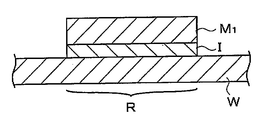
도 4는 게이트 절연막과 하부 도전체막이 형성된 웨이퍼의 종단면도.4 is a longitudinal sectional view of a wafer on which a gate insulating film and a lower conductor film are formed.
도 5는 도 4의 하부 도전체막상에 강유전체막이 형성된 웨이퍼의 종단면도.5 is a longitudinal cross-sectional view of a wafer in which a ferroelectric film is formed on the lower conductor film of FIG.
도 6은 도 5의 강유전체막상에 상부 도전체막이 형성된 웨이퍼의 종단면도.6 is a longitudinal cross-sectional view of a wafer in which an upper conductor film is formed on the ferroelectric film of FIG.
도 7은 도 1의 스퍼터링 장치와 도 2의 어닐링 장치를 이용하여 제조된 강유전체막의 히스테리시스 특성을 도시한 그래프.7 is a graph showing the hysteresis characteristics of the ferroelectric film manufactured by using the sputtering apparatus of FIG. 1 and the annealing apparatus of FIG.
도 8은 도 7의 강유전체막의 C-E 특성을 도시한 그래프.FIG. 8 is a graph showing C-E characteristics of the ferroelectric film of FIG. 7. FIG.
도 9는 플라즈마 처리 장치의 종단면도.9 is a longitudinal sectional view of the plasma processing apparatus;
도 10은 얇은 하층 강유전체막이 형성된 웨이퍼의 종단면도.10 is a longitudinal sectional view of a wafer on which a thin lower layer ferroelectric film is formed.
도 11은 하층 강유전체막에 산소 라디칼에 의해 산소가 도입된 웨이퍼의 종단면도.Fig. 11 is a longitudinal sectional view of a wafer in which oxygen is introduced by oxygen radicals into an underlying ferroelectric film.
도 12는 도 11의 하층 강유전체막상에 상층 강유전체막이 형성된 웨이퍼의 종단면도.12 is a longitudinal cross-sectional view of a wafer in which an upper ferroelectric film is formed on the lower ferroelectric film of FIG.
도 13은 플라즈마 처리를 행한 하층 강유전체막을 갖는 강유전체막과, 플라 즈마 처리를 행하지 않는 강유전체막과의 히스테리시스 특성을 비교한 그래프.Fig. 13 is a graph comparing hysteresis characteristics between a ferroelectric film having a lower layer ferroelectric film subjected to plasma treatment and a ferroelectric film not subjected to plasma treatment.
도 14는 도 13의 강유전체막의 C-E 특성을 도시한 그래프.14 is a graph showing the C-E characteristics of the ferroelectric film of FIG.
도 15는 전계 인가 수단을 구비한 어닐링 장치의 종단면도.15 is a longitudinal cross-sectional view of the annealing apparatus with field application means.
도 16은 웨이퍼에 전계를 인가한 상태를 도시한 웨이퍼의 종단면도.Fig. 16 is a longitudinal sectional view of the wafer showing a state in which an electric field is applied to the wafer.
본 발명은 강유전체막, 반도체 장치, 강유전체막의 제조 방법 및 강유전체막의 제조 장치에 관한 것이다.The present invention relates to a ferroelectric film, a semiconductor device, a method for producing a ferroelectric film, and a device for producing a ferroelectric film.
비휘발성의 반도체 메모리로서, 강유전체의 자발 분극 상태를 이용한 강유전체 메모리가 있다. 이 강유전체 메모리는 전계의 부가에 의해 야기되는 2개의 안정된 전기 분극 상태를 "0", "1"에 대응시킴으로써 기억시키고 있다. 이 강유전체 메모리는 다른 비휘발성 메모리에 비하여 소비전력이 적고, 고속 동작이 가능한 것으로 알려져 있다.As a nonvolatile semiconductor memory, there is a ferroelectric memory using a spontaneous polarization state of a ferroelectric. This ferroelectric memory stores two stable electric polarization states caused by the addition of an electric field by corresponding to "0" and "1". It is known that this ferroelectric memory consumes less power and can operate at higher speed than other nonvolatile memories.
강유전체 메모리는 예컨대 커패시터 부분에 강유전체막을 갖고 있고, 예컨대 전계 효과형 트랜지스터(FET)형의 강유전체 메모리에는 실리콘 반도체 기판의 채널 형성 영역상에 게이트 절연막, 하부 도전체막, 강유전체막, 상부 도전체막이 차례로 적층되어 있는 것(MFMIS-FET)이나 실리콘 반도체 기판상에 게이트 절연막, 강유전체막, 상부 도전체막이 차례로 적층되어 있는 것(MFIS-FET)이 있다.The ferroelectric memory has, for example, a ferroelectric film in a capacitor portion. For example, in a ferroelectric memory of a field effect transistor (FET) type, a gate insulating film, a lower conductor film, a ferroelectric film, and an upper conductor film are sequentially stacked on a channel formation region of a silicon semiconductor substrate. The gate insulating film, the ferroelectric film, and the upper conductor film are stacked in this order (MFMIS-FET) or on a silicon semiconductor substrate (MFIS-FET).
상기 강유전체막의 막 재료로는 종래부터 Pb2(Zr1 - xTix)(O≤x≤1)(이하 "PZT"라고 함), SrBi2Ta2O9(이하 "SBT"라고 함) 등의 강유전체 재료가 사용되어 왔지만, 최근, 비교적 비유전율을 낮게 억제할 수 있는 동시에 쉽게 나빠지지 않는 Sr, Ta, Nb를 주성분으로 하는 Sr2(Ta1 - xNbx)O7(0≤x≤1)(이하 "STN"이라 함)가 주목되고 있다.As the film material of the ferroelectric film, Pb 2 (Zr 1 - x Ti x ) (O ≦ x ≦ 1) (hereinafter referred to as “PZT”), SrBi 2 Ta 2 O 9 (hereinafter referred to as “SBT”), etc. Although ferroelectric materials have been used, Sr 2 (Ta 1 - x Nb x ) O 7 (0≤x≤) mainly composed of Sr, Ta, and Nb, which can suppress relatively low dielectric constant and not easily deteriorate. 1) (hereinafter referred to as "STN") is paying attention.
그런데, 현재, STN 강유전체막의 성막 방법으로서, 강유전체 재료의 전구체 용액을 도포하고, 건조하여 유기물을 증발시킨 후, 고온으로 가열하여 산화시켜 결정화하는 졸-겔법이 이용되고 있다(예컨대, 일본 특허 공개 공보 제10-326872호). STN은 이온화 에너지가 높은 Ta나 Nb로 조성되어 있기 때문에, Ta나 Nb 원자의 산화에는 매우 높은 에너지가 필요하다. 상기 졸-겔법이 채용되고 있는 것은 처음부터 전구체내에 산소 성분을 함유하여 비교적 산화 에너지가 적게 들기 때문이다.By the way, as a film-forming method of a STN ferroelectric film, the sol-gel method which apply | coats the precursor solution of a ferroelectric material, dries, evaporates organic substance, heats it, heats, oxidizes, and crystallizes is used (for example, Japanese Unexamined Patent Publication) 10-326872). Since STN is composed of Ta or Nb having high ionization energy, very high energy is required for oxidation of Ta or Nb atoms. The sol-gel method is employed because oxygen component is contained in the precursor from the beginning, so that the oxidizing energy is relatively low.
그러나, 전술한 졸-겔법을 이용하여 성막된 STN 강유전체막은 현재 보고되어 있는 것으로서, 비유전율이 40이고, 강유전성을 나타내는 항전계(抗電界)가 50 kV/㎝인 것이 최량이며, 그 이상의 특성을 갖는 것은 실현되지 않았다.However, the STN ferroelectric film formed by using the above-mentioned sol-gel method is currently reported, and it is best that the relative dielectric constant is 40 and the constant electric field exhibiting ferroelectricity is 50 kV / cm. Having is not realized.
강유전체 메모리는 강유전체막에 전계를 걸거나 전계를 제거하거나 함으로써 안정된 분극 상태를 야기하는 것으로서, 강유전체막을 보다 저소비 전력으로 분극시키기 위해서는 강유전체막의 비유전율을 보다 작게 할 필요가 있다. 또한, 강유전체 메모리의 기억 등의 동작을 보다 안정되게 행하기 위해서는 강유전체막의 항 전계를 크게 할 필요가 있다. 이와 같이 반도체 메모리의 저소비 전력화, 동작의 안정화를 도모하기 위해서 비유전율이 더욱 낮고, 항전계가 높은 강유전체막의 개발이 중요한 과제가 되고 있다.The ferroelectric memory causes a stable polarization state by applying an electric field to or removing an electric field from the ferroelectric film. In order to polarize the ferroelectric film at a lower power consumption, the relative dielectric constant of the ferroelectric film needs to be made smaller. In addition, in order to more stably perform operations such as storage of the ferroelectric memory, it is necessary to increase the electric field of the ferroelectric film. In order to reduce the power consumption and stabilize the operation of the semiconductor memory, development of a ferroelectric film having a lower relative dielectric constant and a higher electric field has become an important problem.
본 발명은 이러한 점을 감안하여 이루어진 것으로서, 비유전율이 더욱 낮고, 항전계가 큰 STN 강유전체막, 이 강유전체막을 갖는 반도체 장치, 강유전체막의 제조 방법 및 강유전체막의 제조 장치를 제공하는 것을 그 목적으로 한다.This invention is made | formed in view of such a point, Comprising: It aims at providing the STN ferroelectric film with a lower dielectric constant and a large constant electric field, the semiconductor device which has this ferroelectric film, the manufacturing method of a ferroelectric film, and the manufacturing apparatus of a ferroelectric film.
상기 목적을 달성하기 위해서 본 발명의 강유전체막은 막 재료로서 Sr, Ta, Nb를 주성분으로 하는 강유전체 재료가 사용되며, 비유전율이 40 미만이면서 항전계가 50 kV/㎝를 초과하는 것이다.In order to achieve the above object, the ferroelectric film of the present invention is a ferroelectric material containing Sr, Ta, and Nb as a main component, and has a relative dielectric constant of less than 40 and a constant electric field of more than 50 kV / cm.
발명자들의 검증에 따르면, 스퍼터링 처리를 행하는 처리실의 타겟 주변의 내측 표면을 타겟과 동일한 재질로 형성하고, 그 처리실내에서 스퍼터링 처리에 의해 하지(下地)의 표면에 강유전체막을 형성하며, 그 후, 이 강유전체막을 가열하여, 산화시킴으로써, 비유전율이 40 미만이고, 항전계가 50 kV/㎝를 초과하는 STN 강유전체막이 제조되는 것을 알 수 있었다. 이 강유전체막에 의해 예컨대 보다 전력 소비량이 적으면서 동작이 안정된 강유전체 메모리를 제조할 수 있다.According to the verification of the inventors, the inner surface of the periphery of the target of the processing chamber to be subjected to the sputtering treatment is formed of the same material as the target, and the ferroelectric film is formed on the surface of the underlying substrate by the sputtering treatment in the processing chamber. It was found that by heating and oxidizing the ferroelectric film, an STN ferroelectric film having a relative dielectric constant of less than 40 and a constant electric field exceeding 50 kV / cm was produced. The ferroelectric film can, for example, produce a ferroelectric memory with a lower power consumption and more stable operation.
상기 강유전체막은 산소 라디칼에 의해 산소 성분이 도입된 막층을 갖고 있어도 좋다. 이러한 경우, 강유전체막의 일부 막층에 산소 성분이 도입되기 때문에, 강유전체막내의 산소 성분이 부족하지 않게 되어 강유전체막의 산화가 충분히 행해진다. 따라서, 강유전체막에 STN과 같은 이온화 에너지가 높은 원자를 갖는 막 재 료를 사용하여도 산화가 충분히 행해져서 항전계 등의 특성 향상이 도모된다.The ferroelectric film may have a film layer in which an oxygen component is introduced by oxygen radicals. In such a case, since an oxygen component is introduced into some of the film layers of the ferroelectric film, the oxygen component in the ferroelectric film is not insufficient, and the ferroelectric film is sufficiently oxidized. Therefore, even when a film material having atoms with high ionization energy such as STN is used in the ferroelectric film, oxidation is sufficiently performed to improve characteristics such as a constant electric field.
상기 강유전체막의 막층은 희가스 성분을 함유하고 있어도 좋다. 또한, 그 희가스 성분은 크립톤(Kr)이 바람직하다.The film layer of the ferroelectric film may contain a rare gas component. In addition, the rare gas component is preferably krypton (Kr).
본 발명의 강유전체막을 갖는 반도체 장치는 강유전체막의 막 재료로서 Sr, Ta, Nb를 주성분으로 하는 강유전체 재료가 사용되며, 상기 강유전체막의 비유전율이 40 미만이면서 항전계가 50 kV/㎝를 초과하고 있다.In the semiconductor device having the ferroelectric film of the present invention, a ferroelectric material containing Sr, Ta, and Nb as a main component is used as the film material of the ferroelectric film. The ferroelectric film has a relative dielectric constant of less than 40 and a constant electric field of more than 50 kV / cm.
상기 반도체 장치의 강유전체막은 산소 라디칼에 의해 산소 성분이 도입된 막층을 갖고 있어도 좋다. 상기 강유전체막의 막층은 희가스 성분을 함유하고 있어도 좋다. 상기 희가스 성분은 크립톤(Kr)이어도 좋다. 이들 반도체 장치의 강유전체막의 하지의 재료로는 금속 산화물이 사용되어도 좋다.The ferroelectric film of the semiconductor device may have a film layer in which an oxygen component is introduced by oxygen radicals. The film layer of the ferroelectric film may contain a rare gas component. Krypton (Kr) may be sufficient as the said rare gas component. As the underlying material of the ferroelectric film of these semiconductor devices, a metal oxide may be used.
또한, 상기 반도체 장치는 상기 강유전체막의 양면에 상기 강유전체막이 사이에 끼워져 있도록 상부 도전체막과 하부 도전체막을 가지며, 상기 강유전체막, 상기 상부 도전체막 및 상기 하부 도전체막에 의해 커패시터가 형성되어 있어도 좋다. 또한, 상기 반도체 장치는 게이트에 상기 커패시터가 접속된 전계 효과형 트랜지스터를 갖고 있어도 좋다.The semiconductor device may have an upper conductor film and a lower conductor film so as to sandwich the ferroelectric film on both surfaces of the ferroelectric film, and a capacitor may be formed by the ferroelectric film, the upper conductor film, and the lower conductor film. The semiconductor device may have a field effect transistor in which the capacitor is connected to a gate.
본 발명의 강유전체막의 제조 방법은 처리실의 적어도 타겟 주변의 내측 표면이 타겟과 동일한 구성 재질로 형성되어 있는 처리실내에서 타겟에 대하여 플라즈마 속의 이온을 충돌시키고, 그 충돌에 의해 발생한 타겟 원자를 하지에 퇴적시킴으로써, 강유전체막을 형성하는 막형성 공정과, 상기 강유전체막을 가열하여 산화시키는 가열 공정을 갖고 있다.The method of manufacturing the ferroelectric film of the present invention collides ions in a plasma with respect to a target in a processing chamber in which at least the inner surface of the target periphery of the processing chamber is formed of the same constituent material as the target, and deposits the target atoms generated by the collision on the substrate. The film forming step of forming a ferroelectric film, and the heating step of heating and oxidizing the ferroelectric film.
발명자들의 검증에 따르면, 본 발명과 같이, 처리실의 내측 표면의 타겟 주변을 타겟과 동일한 구성 재질로 형성하고, 그 처리실내에서 스퍼터링 처리에 의해 강유전체막의 막형성을 행하며, 그 후 강유전체막을 가열하여 산화시킴으로써, 종래보다 비유전율이 낮고, 항전계가 크게 강유전체막이 제조되는 것을 알 수 있었다. 본 발명과 같은 스퍼터링법에 의한 성막 방법에서는, 플라즈마 속의 이온이 잘못하여 타겟 주변에 충돌하는 경우가 있다. 본 발명에 따르면, 타겟 주변을 타겟과 동일한 재질로 형성하였기 때문에, 그 타겟 주변에 이온이 충돌하더라도, 타겟에 충돌한 경우와 동일한 타겟 원자가 튀어나온다. 이 결과, 하지상에 불순물이 없는 고순도의 강유전체막이 형성되고, 비유전율이 낮고, 항전계가 높은 양질의 강유전체막이 형성되는 것으로 생각된다.According to the verification of the inventors, as in the present invention, the target periphery of the inner surface of the processing chamber is formed of the same constituent material as the target, and the ferroelectric film is formed by sputtering in the processing chamber, and then the ferroelectric film is heated to oxidize. In this case, it was found that the ferroelectric film was produced with a lower relative dielectric constant and a larger electric field than before. In the film forming method by the sputtering method as in the present invention, ions in the plasma may be accidentally collided around the target. According to the present invention, since the periphery of the target is formed of the same material as that of the target, even if ions collide with the target, the same target atoms come out as if they collided with the target. As a result, it is considered that a high-purity ferroelectric film free of impurities is formed on the base, and a high-quality ferroelectric film having a low relative dielectric constant and a high constant electric field is formed.
상기 강유전체막의 제조 방법에 있어서의 상기 막형성 공정은 하지상에 비교적 얇은 하층 강유전체막을 형성하는 제1 막형성 공정과, 그 후, 상기 하층 강유전체막에 플라즈마에 의해 발생시킨 산소 라디칼에 의해 산소 성분을 도입하는 산소 도입 공정과, 그 후, 상기 하층 강유전체막 위에 비교적 두꺼운 상층 강유전체막을 형성하는 제2 막형성 공정을 갖고 있어도 좋다. 이러한 경우, 강유전체막의 하층에 산소 성분이 도입된 얇은 하층 강유전체막이 형성된다. 이 하층 강유전체막은 상층 강유전체막내의 산소 성분이 하지측으로 확산되는 것을 방지하는 확산 방지층으로서의 기능을 수행한다. 따라서, 강유전체막 속의 산소 성분이 하지측으로 유출되는 일이 없게 되기 때문에, 강유전체막이 충분히 산화되어 항전계가 높은 양질의 막이 형성된다.The film forming step in the method of manufacturing the ferroelectric film includes a first film forming step of forming a relatively thin lower layer ferroelectric film on a base and an oxygen component generated by plasma generated in the lower layer ferroelectric film by plasma thereafter. You may have the oxygen introduction process to introduce | transduce, and the 2nd film formation process of forming a comparatively thick upper ferroelectric film on the said lower layer ferroelectric film after that. In this case, a thin lower layer ferroelectric film into which an oxygen component is introduced is formed in the lower layer of the ferroelectric film. This lower layer ferroelectric film functions as a diffusion barrier layer that prevents the diffusion of oxygen components in the upper ferroelectric film to the underside. Therefore, since the oxygen component in the ferroelectric film does not flow out to the underside, the ferroelectric film is sufficiently oxidized to form a high quality film having a high constant electric field.
상기 강유전체막의 제조 방법에 있어서의 상기 가열 공정은 강유전체막을 결정화시키기 위한 결정화 공정과, 강유전체막상에 상부막이 형성된 후에 상기 강유전체막의 산소 성분량을 회복시키기 위한 산소 성분 회복 공정을 갖고 있어도 좋다.The heating step in the method of manufacturing the ferroelectric film may have a crystallization step for crystallizing the ferroelectric film and an oxygen component recovery step for restoring the oxygen content of the ferroelectric film after the upper film is formed on the ferroelectric film.
상기 산소 성분 회복 공정에서는, 플라즈마에 의해 발생시킨 산소 라디칼에 의해 강유전체막이 산화되어도 좋다. 이러한 경우, 산소 라디칼에 의해 강유전체막이 보다 강한 산화력으로 산화되기 때문에, 비교적 저온의 가열에 의해 강유전체막의 산소 성분량을 회복할 수 있다.In the oxygen component recovery step, the ferroelectric film may be oxidized by oxygen radicals generated by the plasma. In this case, since the ferroelectric film is oxidized with stronger oxidizing power by oxygen radicals, the oxygen component amount of the ferroelectric film can be recovered by relatively low temperature heating.
상기 강유전체막의 제조 방법은 상기 강유전체막의 온도가 퀴리 온도 이상이 되도록 상기 강유전체막을 가열하고, 그 후 그 강유전체막의 온도가 하강하여 강유전체막의 온도가 퀴리 온도를 통과할 때에, 상기 강유전체막에 소정 방향의 전계를 인가하는 공정을 갖고 있어도 좋다. 이와 같이 퀴리 온도의 통과시에 강유전체막에 전계를 인가함으로써, 강유전체막내의 분극축이 한 방향으로 된다. 이 결과, 항전계가 큰 양질의 강유전체막이 제조된다. 또한, 상기 "퀴리 온도를 통과할 때"에는 퀴리 온도가 된 시점에서 전계를 인가하는 경우뿐만 아니라, 퀴리 온도가 되기 이전부터 전계를 인가하는 경우도 포함된다.The method of manufacturing the ferroelectric film includes heating the ferroelectric film so that the temperature of the ferroelectric film is equal to or greater than the Curie temperature, and then, when the temperature of the ferroelectric film is lowered and the temperature of the ferroelectric film passes through the Curie temperature, an electric field in a predetermined direction is applied to the ferroelectric film. It may have a process of applying. In this way, when an electric field is applied to the ferroelectric film when the Curie temperature passes, the polarization axis in the ferroelectric film is in one direction. As a result, a good ferroelectric film having a large constant electric field is produced. In addition, the "when passing through the Curie temperature" includes not only the case of applying the electric field at the time when the Curie temperature is reached, but also the case of applying the electric field before the Curie temperature is reached.
또한, 상기 강유전체막의 제조 방법은 상기 강유전체막의 막 재료로서 Sr, Ta, Nb를 주성분으로 하는 강유전체 재료가 사용되며, 상기 처리실의 적어도 타겟 주변의 내측 표면은 Sr, Ta, Nb를 주성분으로 하는 재질로 형성되어 있어도 좋다.In addition, a ferroelectric material including Sr, Ta, and Nb as a main component is used as a method of manufacturing the ferroelectric film, and at least an inner surface around the target of the processing chamber is made of Sr, Ta, and Nb as a main component. It may be formed.
또한, 다른 관점에 따르면, 본 발명의 강유전체막의 제조 방법은 강유전체막 의 온도가 퀴리 온도 이상이 되도록 강유전체막의 온도를 상승시키고, 그 후, 그 강유전체막의 온도가 하강하여 강유전체막의 온도가 퀴리 온도를 통과할 때에, 강유전체막에 소정 방향의 전계를 인가한다.According to another aspect, in the method of manufacturing the ferroelectric film of the present invention, the temperature of the ferroelectric film is raised so that the temperature of the ferroelectric film is equal to or more than the Curie temperature, and then the temperature of the ferroelectric film is lowered so that the temperature of the ferroelectric film passes the Curie temperature. In doing so, an electric field in a predetermined direction is applied to the ferroelectric film.
본 발명에 따르면, 전계의 인가에 의해 강유전체막내의 분극축이 한 방향으로 된다. 이 결과, 보다 항전계가 큰 양질의 강유전체막이 형성된다.According to the present invention, the polarization axis in the ferroelectric film is in one direction by application of an electric field. As a result, a higher-quality ferroelectric film having a larger constant electric field is formed.
본 발명의 강유전체막의 제조 장치는 피처리체를 수용하는 처리실에서 타겟에 플라즈마 속의 이온을 충돌시키고, 그 충돌에 의해 튀어나온 타겟 원자를 피처리체에 퇴적시킴으로써, 피처리체에 강유전체막을 형성하며, 상기 처리실의 내측 표면의 적어도 상기 타겟 주변부는 상기 타겟과 동일한 구성 재질로 형성되어 있다.An apparatus for manufacturing a ferroelectric film of the present invention collides ions in a plasma with a target in a processing chamber containing a target object, and deposits target atoms protruding by the collision onto the target object to form a ferroelectric film on the target object. At least the target periphery of the inner surface is formed of the same constituent material as the target.
본 발명에 따르면, 이온이 잘못하여 타겟을 벗어나 타겟 주변에 충돌한 경우라도, 그 충돌부에서 타겟과 동일한 원자가 튀어나온다. 이 결과, 피처리체에 퇴적되는 강유전체막에 불순물이 혼입되지 않아 순도가 높은 강유전체막이 형성된다. 발명자들의 검증에 따르면, 이러한 강유전체막의 제조 장치를 이용함으로써 비유전율이 낮고, 항전계가 높은 고품질의 강유전체막이 형성되는 것이 확인되고 있다.According to the present invention, even when ions accidentally escape the target and collide around the target, the same atom as the target is protruded from the collision portion. As a result, impurities are not mixed in the ferroelectric film deposited on the object to be processed, thereby forming a ferroelectric film with high purity. According to the verification of the inventors, it is confirmed by using such a ferroelectric film production apparatus that a high-quality ferroelectric film having a low relative dielectric constant and a high constant electric field is formed.
상기 강유전체막의 제조 장치에 있어서, 상기 타겟의 주변부에는 상기 타겟과 동일한 구성 재질의 보호 부재가 부착되어 있어도 좋다. 또한, 상기 강유전체막의 제조 장치에서는, 상기 강유전체막의 막 재료로서 Sr, Ta, Nb를 주성분으로 하는 강유전체 재료가 사용되고 있고, 상기 타겟과 동일한 구성 재질은 Sr, Ta, Nb를 주성분으로 하는 재질이어도 좋다.In the apparatus for producing a ferroelectric film, a protective member made of the same material as that of the target may be attached to the peripheral portion of the target. In the ferroelectric film production apparatus, a ferroelectric material containing Sr, Ta, and Nb as a main component is used as a film material of the ferroelectric film, and the same constituent material as the target may be a material containing Sr, Ta, and Nb as a main component.
또한, 다른 관점에 따르면, 본 발명의 강유전체막의 제조 장치는 강유전체막을 퀴리 온도 이상으로 가열하기 위한 가열 수단과, 퀴리 온도 이상이 된 강유전체막의 온도가 하강하여 강유전체막의 온도가 상기 퀴리 온도를 통과할 때에, 그 강유전체막에 소정 방향의 전계를 인가하기 위한 전계 인가 수단을 구비한다. 상기 강유전체막의 막 재료로서 Sr, Ta, Nb를 주성분으로 하는 강유전체 재료가 사용되어도 좋다.According to another aspect, the apparatus for producing a ferroelectric film of the present invention is characterized in that the heating means for heating the ferroelectric film above the Curie temperature and the temperature of the ferroelectric film that has become the Curie temperature or higher fall so that the temperature of the ferroelectric film passes through the Curie temperature. And electric field applying means for applying an electric field in a predetermined direction to the ferroelectric film. As a film material of the ferroelectric film, a ferroelectric material containing Sr, Ta, and Nb as a main component may be used.
이하, 본 발명의 실시 형태에 대해서 설명한다. 도 1은 본 발명의 강유전체막의 제조 방법을 실시하기 위해서 이용한 강유전체막의 제조 장치로서의 스퍼터링 장치(1)의 종단면의 상태를 모식적으로 도시하고 있다. 도 2는 어닐링 장치(2)의 종단면의 상태를 모식적으로 도시하고 있다.EMBODIMENT OF THE INVENTION Hereinafter, embodiment of this invention is described. Fig. 1 schematically shows the state of the longitudinal cross section of the
스퍼터링 장치(1)는 예컨대 상부가 개구되고, 바닥이 있는 원통 형상의 처리 용기(10)와, 처리 용기(10)의 상부를 폐쇄할 수 있는 덮개(11)를 구비하고 있다. 덮개(11)에 의해 처리 용기(10)의 상부를 폐쇄함으로써 처리실(S)이 형성된다. 처리 용기(10)의 저부에는 강유전체막이 형성되는 피처리체로서의 기판, 예컨대 반도체 웨이퍼(이하 "웨이퍼"라 함)(W)를 얹어 놓는 적재대(12)가 마련되어 있다. 이 적재대(12)에는 도시하지 않은 흡인 수단이 마련되어 있고, 적재대(12)는 얹어 놓은 웨이퍼(W)를 흡착 유지할 수 있다.The
적재대(12)와 대향하는 처리실(S)의 천정면, 즉 덮개(11) 하면의 중앙부에는, 예컨대 오목부(11a)가 마련되어 있고, 이 오목부(11a)에는 전극(13)이 매설되어 있다. 전극(13)은 처리 용기(10)의 외부에 설치된 고주파 전원(14)으로부터의 전압을 자유자재로 인가할 수 있도록 되어 있다. 전극(13)의 하면, 즉 적재대(12)와 대향하는 면에는 타겟(15)이 마련되어 있다. 타겟(15)의 재질은 웨이퍼(W)에 형성되는 강유전체막의 종류에 따라 정해져 있고, STN{Sr2(Ta1 - xNbx)O7(0≤x≤1)}의 강유전체막을 형성하는 본 실시 형태에 있어서는, 타겟(15)의 재질로는 Sr, Ta, Nb를 주성분으로 하는 Sr2 .5(Ta0 .7Nb0 .3)2O7이 사용된다.The recessed
예컨대 처리 용기(10)의 일단 측면에는 처리 가스 도입구(20)가 마련되어 있고, 처리 가스 도입구(20)에는 처리 가스 공급원(21)으로 통하는 처리 가스 공급관(22)이 접속되어 있다. 처리 가스 공급관(22)에는 밸브(23), 매스플로우 컨트롤러(24)가 마련되어 있고, 처리실(S)내에는 소정 압력의 처리 가스를 공급할 수 있다. 본 실시 형태에 있어서는 처리 가스 공급원(21)에 처리 가스로서 산소 가스(O2)와 희가스인 아르곤(Ar) 가스의 각 공급원(25, 26)이 접속되어 있다. 또한, 아르곤(Ar) 가스 대신에 크립톤(Kr), 크세논(Xe) 등의 다른 희가스를 사용하여도 좋다.For example, a
상기 처리 가스 도입구(20)에 대향하는 처리 용기(10)의 타단 측면에는 처리실(S)내를 배기하기 위한 배기구(30)가 마련되어 있다. 배기구(30)에는 진공 펌프 등의 배기 장치(31)로 통하는 배기관(32)이 접속되어 있다. 이 배기구(30)로부터의 배기에 의해 예컨대 처리실(S)내를 소정의 압력으로 감압할 수 있다.An
전극(13)의 고주파 전압에 의해 처리실(S)내에 공급된 처리 가스가 플라즈마화하여 아르곤 이온이 발생한다. 전극(13)의 전위를 부전위로 유지함으로써, 정전하의 아르곤 이온이 타겟(15)측을 향해 비상하여 충돌한다. 이 충돌에 의해 타 겟(15)으로부터 타겟 원자인 STN 퇴적종(堆積種)이 튀어나온다. 이 아르곤 이온이 충돌할 가능성이 있는 부분, 예컨대 덮개(11) 하면의 타겟(15) 주변부에는 타겟(15)과 동일한 구성 재질로 형성된 보호 부재(35)가 부착되어 있다. 즉, 보호 부재(35)는 Sr, Ta, Nb를 주성분으로 하는 Sr2 .5(Ta0 .7Nb0 .3)2O7의 재질로 형성되어 있다. 이렇게 함으로써, 아르곤 이온이 잘못하여 타겟(15)의 주변부에 충돌하더라도, 그 충돌부에서 STN 퇴적종 이외의 다른 불순물이 튀어나오는 일이 없다.By the high frequency voltage of the
또한, 처리 가스가 플라즈마화되었을 때에, 처리실(S)내에는 산소 라디칼이 발생한다. 타겟(15)으로부터 튀어나온 STN 퇴적종은 이 산소 라디칼에 의해 산화되어 웨이퍼(W) 표면에 퇴적된다. 처리실(S)에서의 산소 라디칼에 노출되는 부분, 예컨대 처리실(S)의 내측 표면으로서 웨이퍼(W)의 높이보다 높은 부분에는 석영 피막(K)이 피복되어 있다. 이 석영 피막(K)에 의해 산소 라디칼의 소실이 억제되어, 처리실(S)내의 STN 퇴적종이 보다 확실하게 산화된다.In addition, oxygen radicals are generated in the processing chamber S when the processing gas is converted into plasma. The STN deposited species protruding from the
한편, 어닐링 장치(2)는 도 2에 도시된 바와 같이 예컨대 축이 수평 방향으로 향해진 거의 원통 형상의 케이스(40)를 갖는다. 케이스(40)의 축 방향의 측면부(40a, 40b)는 플랜지에 의해 폐쇄되어 있고, 케이스(40)내에는 폐쇄된 처리실(H)이 형성되어 있다. 케이스(40)내의 중앙부에는 웨이퍼(W)를 얹어 놓는 적재판(41)이 마련되어 있다. 케이스(40)의 직경 방향의 측면을 덮는 원통부(40c)는 두께가 두껍게 형성되고, 그 속에 히터(42)가 내장되어 있다. 히터(42)는 도 3에 도시된 바와 같이 원통부(40c)의 전 둘레에 걸쳐 균등하게 내장되어 있고, 적재판(41)상의 웨이퍼(W)를 전 둘레 방향에서 균등하게 가열할 수 있다. 도 2에 도시된 바와 같이 히터(42)는 케이스(40) 외부에 설치된 전원(43)에 접속되어 있고, 이 전원(43)으로부터의 급전에 의해 발열한다. 전원(43)은 예컨대 온도 컨트롤러(44)에 의해 제어되고, 온도 컨트롤러(44)는 전원(43)의 급전 출력을 바꿈으로써 히터(42)의 온도를 제어할 수 있다. 예컨대 적재판(41)에는 온도 센서로서의 열전대(T)가 마련되어 있다. 열전대(T)에 의한 온도 측정 결과는 온도 컨트롤러(44)에 출력할 수 있고, 온도 컨트롤러(44)는 이 온도 측정 결과에 기초하여 히터(42) 온도를 조정할 수 있다.On the other hand, the
케이스(40)의 일단 측면부(40a)에는 처리 가스 도입구(45)가 개구되어 있고, 처리 가스 도입구(45)에는 처리 가스 공급원(46)으로 통하는 처리 가스 공급관(47)이 접속되어 있다. 처리 가스 공급관(47)에는 밸브(48), 매스플로우 컨트롤러(49)가 마련되어 있고, 처리실(H)내에 소정 압력의 처리 가스를 공급할 수 있다. 본 실시 형태에 있어서는 처리 가스 공급원(46)에 처리 가스로서의 산소 가스와 아르곤가스의 각 공급원(50, 51)이 접속되어 있다. 또한, 아르곤 가스 대신에 질소 가스(N2)를 사용하여도 좋다.A
처리 가스 도입구(45)에 대향하는 케이스(40)의 타단 측면부(40b)에는 케이스(40)의 외부에 설치된 배기 장치(52)로 통하여 처리실(H)내의 분위기를 배기하기 위한 배기구(53)가 마련되어 있다.An
스퍼터링 장치(1)와 어닐링 장치(2)는 이상과 같은 구성을 갖고 있고, 다음 에 본 발명의 실시 형태에 따른 강유전체막의 제조 방법을, 반도체 장치로서의 강유전체 메모리를 제조하는 경우를 예를 들어 설명한다.The
본 실시 형태에 있어서의 강유전체 메모리는 예컨대 전계 효과형 트랜지스터를 이용한 반도체 메모리로서, 예컨대 도 4에 도시된 바와 같이 실리콘(Si)으로 이루어진 웨이퍼(W)의 채널 영역(R)상에 산화실리콘(SiO2) 게이트로서의 게이트 절연막(I)이 형성된다. 게이트 절연막(I)상에 금속 산화막, 예컨대 IrO2막으로 이루어진 하부 도전체막(M1)이 형성된다. 이 하부 도전체막(M1)은 후술하는 강유전체막의 하지막으로서 형성된다. 또한, 이 하부 도전체막(M1)은 후술하는 강유전체막과 동일한 스퍼터링 처리에 의해 형성되어도 좋다.The ferroelectric memory in this embodiment is, for example, a semiconductor memory using a field effect transistor, for example, silicon oxide (SiO) on the channel region R of the wafer W made of silicon (Si) as shown in FIG. 2 ) A gate insulating film I is formed as a gate. A lower conductor film M 1 made of a metal oxide film, such as an IrO 2 film, is formed on the gate insulating film I. The lower conductor film M 1 is formed as an underlayer of the ferroelectric film described later. The lower conductor film M 1 may be formed by the same sputtering process as the ferroelectric film described later.
하부 도전체막(M1)이 형성된 웨이퍼(W)는 스퍼터링 장치(1)로 반송되어 도 1에 도시된 바와 같이 적재대(12)상에 유지된다. 웨이퍼(W)가 적재대(12)에 유지되면, 배기구(30)로부터 처리실(S)내의 기체가 배기되고, 처리실(S)내가 예컨대 4 Pa 정도로 감압된다. 처리 가스 공급구(20)로부터는 아르곤 가스와 산소 가스가 공급되어 처리실(S)내가 아르곤 가스와 산소 가스로 채워진다. 계속해서, 전극(13)에 부전위의 고주파 전압이 인가되고, 이 고주파 전압에 의해 처리실(S)내의 가스가 플라즈마화되며, 아르곤 가스는 아르곤 이온이 된다. 이 아르곤 이온은 부전위의 전극(13)측으로 끌어당겨져 고속으로 타겟(15)에 충돌한다. 타겟(15)에 아르곤 이온이 충돌하면, 타겟(15)으로부터 STN 퇴적종이 튀어나온다. 이 튀어나온 STN 퇴적 종은 산소 가스가 플라즈마가 됨에 따라 발생한 산소 라디칼에 의해 산화되어 웨이퍼(W)의 표면에 퇴적된다. 이렇게 해서 웨이퍼(W)는 스퍼터링 처리되고, 도 5에 도시된 바와 같이 하부 도전체막(M1)상에 STN을 막 재료로 하는 강유전체막(F)이 형성된다.The wafer W on which the lower conductor film M 1 is formed is conveyed to the
이 STN 퇴적종의 퇴적이 소정 시간 계속되고, 하부 도전체막(M1)상에 예컨대 260 ㎚의 강유전체막(F)이 형성되면, 고주파 전압의 인가가 정지되어 스퍼터링 장치(1)에 있어서의 스퍼터링 처리가 종료된다. 스퍼터링 처리가 종료되면, 도 2에 도시된 바와 같이 웨이퍼(W)는 어닐링 장치(2)로 반송되어 히터(42)에 의해 미리 예컨대 900℃로 온도가 상승되어 있는 적재판(41)상에 적재된다. 처리 가스 공급구(45)로부터 처리실(H)내에 산소 가스와 아르곤 가스가 도입되는 동시에, 배기구(53)로부터는 처리실(H)내의 기체가 배기된다. 이렇게 해서 처리실(H)내에는 축 방향으로 흐르는 기류가 형성되고, 처리실(H)내가 계속해서 퍼지되는 동시에, 처리실(H)내가 산소 가스와 아르곤 가스의 혼합 가스 분위기로 치환된다. 900℃로 유지된 적재판(41)상에 적재된 웨이퍼(W)는 가열되며, 강유전체막(F)이 산화되어 결정화된다. 강유전체막(F)이 결정화되면, 웨이퍼(W)가 어닐링 장치(2)로부터 취출되고, 어닐링 처리가 종료된다.If the deposition of the STN deposited species continues for a predetermined time, and the ferroelectric film F of, for example, 260 nm is formed on the lower conductor film M 1 , the application of the high frequency voltage is stopped and the sputtering in the
어닐링 처리가 종료되면, 강유전체막(F)상에 도 6에 도시된 바와 같은 상부 도전체막(M2)이 형성된다. 이 상부 도전체막(M2)의 성막은 예컨대 전술한 바와 같은 스퍼터링 처리에 의해 행해진다. 상부 도전체막(M2)이 형성되면, 웨이퍼(W)는 다시 어닐링 장치(2)로 반송되어 산소 가스 분위기내에서 가열된다. 이에 따라, 강유전체막(F)의 표면이 재차 산화되고, 상부 도전체막(M2)의 형성시에 결손된 강유전체막(F) 표면의 산소 성분량이 회복, 보충된다. 그 후, 포토리소그래피 공정 등이 행해져 전계 효과형 트랜지스터형의 강유전체 메모리가 완성된다.When the annealing process is completed, the upper conductor film M 2 as shown in FIG. 6 is formed on the ferroelectric film F. As shown in FIG. The upper conductor film M 2 is formed by, for example, the sputtering process as described above. When the upper conductor film M 2 is formed, the wafer W is conveyed back to the
다음에, 이상의 방법으로 제조된 강유전체 메모리의 강유전체막(F)의 특성을 도 7 및 도 8의 그래프를 이용하여 설명한다. 상기 강유전체막(F)의 스퍼터링 처리에 있어서의 처리 조건은 다음과 같다.Next, the characteristics of the ferroelectric film F of the ferroelectric memory manufactured by the above method will be described using the graphs of FIGS. 7 and 8. The processing conditions in the sputtering process of the ferroelectric film F are as follows.
인가 전압의 주파수: 13.56 MHzFrequency of applied voltage: 13.56 MHz
처리실 압력: 4 Pa(30 mTorr)Process chamber pressure: 4 Pa (30 mTorr)
산소 분압: 6%Oxygen partial pressure: 6%
이 강유전체막(F)의 하지의 하부 도전체막(M1)에는 IrO2가 사용되고, 강유전체막(F)은 타겟(15)의 주변부에 보호 부재(35)가 부착되어 있는 스퍼터링 장치(1)를 이용하여 형성되었다. 도 7은 강유전체막(F)의 히스테리시스(hysteresis) 특성을 나타내는 것으로서, 강유전체막(F)의 항전계(Ec)는 52 kV/㎝였다. 도 8은 강유전체막(F)의 C(Capacitance)-E(Electric field) 특성을 나타내는 것으로서, 강유전체막(F)의 커패시터 면적(S)이 1.2×10⁻³ ㎠이고, 막 두께(df)가 260 ㎚의 조건이며, 강유전체막(F)의 용량(C)은 1.44×10⁻⁴F였다. 이들 수치를 비유전율(εf)을 산출하는 하기 수학식 1에 대입하면, 강유전체막(F)의 비유전율(εf)은 35였다.IrO 2 is used for the lower conductive film M 1 of the base of the ferroelectric film F, and the ferroelectric film F uses the
따라서, 이상에 기재한 강유전체막의 제조 방법에 따르면, 종래에는 없는 비유전율이 40 이하이고 항전계가 50 kV/㎝를 초과하는 강유전체막(F)을 형성할 수 있다. 발명자의 지견에 따르면, 상기 방법에 의해 실현된 비유전율의 저하와 항전계의 상승은 타겟(15)의 주변부에 보호 부재(35)를 부착한 것에 따른다. 이 보호 부재(35)에 의해 아르곤 이온의 충돌부로부터 STN 이외의 퇴적종이 튀어나와 웨이퍼(W)에 퇴적되는 것을 방지할 수 있기 때문에, 강유전체막(F)으로의 불순물 혼입을 방지할 수 있다. 이 결과, 순도가 높은 막이 형성되어 비유전율, 항전계의 향상이 도모되고 있다. 또한, 강유전체막(F)의 하지에 금속 산화막을 사용하였기 때문에, 강유전체막(F)으로부터 하지를 통과하여 산소 성분이 유출되어 강유전체막(F)의 산소 성분이 결손되는 것을 방지할 수 있다. 이 결과, 강유전체막(F)내의 Ta, Nb 원자의 산화가 충분히 행해진다. 이렇게 해서 제조된 강유전체막(F)을 이용한 강유전체 메모리는 예컨대 강유전체막(F)과 그 양측 도전체막(M1, M2)으로 구성되는 커패시터 부분에 전계가 걸리기 쉽게 된다. 이 결과, 보다 작은 전압으로 강유전체막(F)의 분극 상태를 만들어 낼 수 있어 소비전력이 적은 반도체 메모리가 실현된다. 또한, 항전계가 크기 때문에, 분극 상태가 안정된 반도체 메모리가 실현된다.Therefore, according to the method for producing a ferroelectric film described above, a ferroelectric film F having a relative dielectric constant of 40 or less and a constant electric field of more than 50 kV / cm can be formed. According to the inventor's knowledge, the decrease in the relative dielectric constant and the increase in the electric field realized by the above method depend on the attachment of the
이상의 실시 형태에서 기재한 강유전체막의 제조 방법에서는, 한 번의 스퍼터링 처리에 의해 강유전체막(F)을 형성하였지만, 우선, 얇은 하층 강유전체막을 형성하고, 그 얇은 하층 강유전체막에 산소 라디칼에 의해 산소를 도입하여, 그 후 두꺼운 상층 강유전체막을 형성하도록 하여도 좋다. 이러한 경우를 제2 실시 형태로서 설명한다.In the method of manufacturing the ferroelectric film described in the above embodiment, the ferroelectric film F was formed by one sputtering process, but first, a thin lower layer ferroelectric film was formed, and oxygen was introduced into the thin lower layer ferroelectric film by oxygen radicals. After that, a thick upper ferroelectric film may be formed. This case will be described as the second embodiment.
여기서, 강유전체막에 산소 라디칼에 의해 산소를 도입하기 위한 플라즈마 처리 장치에 대해서 설명한다. 도 9는 플라즈마 처리 장치(60)의 종단면의 상태를 모식적으로 도시하고 있고, 이 플라즈마 처리 장치(60)는 예컨대 알루미늄 합금에 의해 형성되어 있다. 플라즈마 처리 장치(60)는 천정부에 개구부를 구비한 거의 원통형의 처리 용기(61)를 구비하고 있다. 이 처리 용기(61)는 접지되어 있다. 이 처리 용기(61)의 저부에는 예컨대 웨이퍼(W)를 얹어 놓기 위한 서셉터(62)가 마련되어 있다. 이 서셉터(62)는 처리 용기(61)의 외부에 설치된 교류 전원(63)으로부터의 급전에 의해 서셉터(62)내의 히터(64)가 발열되어 서셉터(62)상의 웨이퍼(W)를 예컨대 400℃ 정도까지 가열할 수 있다.Here, a plasma processing apparatus for introducing oxygen into the ferroelectric film by oxygen radicals will be described. 9 schematically shows a state of the longitudinal cross section of the
처리 용기(61)의 저부에는 터보 분자 펌프 등의 배기 장치(70)로 통하여 처리 용기(61)내의 기체를 배기하기 위한 배기구(71)가 마련되어 있다. 배기구(71)는 예컨대 처리 용기(61)의 측면부 근처에 마련되어 있다. 배기구(71)의 서셉터(62)를 사이에 둔 반대측으로서, 처리 용기(61)의 천정부에는 공급구(72)가 마련되어 있다. 공급구(72)에는 처리 가스 공급원(73)으로 통하는 공급관(74)이 접속되어 있다. 본 실시 형태에 있어서는 처리 가스 공급원(73)에는 산소 가스와 희가스인 크립톤(Kr) 가스의 각 공급원(75, 76)이 접속되어 있다. 공급구(72)로부터 처리 용기(61)내에 공급된 가스는 서셉터(62)의 웨이퍼(W) 위를 통과하여 배기구(71)로 배 기된다. 또한, 크립톤 가스 대신에 다른 희가스를 사용하여도 좋다.The bottom of the
처리 용기(61)의 상부 개구에는 기밀성을 확보하기 위한 O링 등의 시일재(80)를 통해 예컨대 석영 유리로 이루어진 유전체창(81)이 마련되어 있다. 이 유전체창(81)에 의해 처리 용기(61)가 폐쇄되고, 처리 용기(61)내에 처리 공간(U)이 형성된다.The upper opening of the
유전체창(81)의 상측에는 안테나 부재(82)가 설치되어 있다. 안테나 부재(82)의 상부에는 동축 도파관(83)이 접속되어 있다. 동축 도파관(83)은 처리 용기(61)의 외부에 설치된 마이크로파 공급 장치(84)에 접속되어 있다. 이 마이크로파 공급 장치(84)에 의해 발생시킨 예컨대 2.45 GHz의 마이크로파는 동축 도파관(83)을 통과하여 상기 안테나 부재(82)에 전파되고, 유전체창(81)을 통해 처리 공간(U) 내로 방사된다. 처리 용기(61)의 측부에는 웨이퍼(W)를 반입 및 반출하기 위한 반입출구(90)와, 이 반입출구(90)를 개폐하는 셔터(91)가 설치되어 있다.An
다음에, 제2 실시 형태에 있어서의 강유전체막의 제조 방법에 대해서 설명하면, 예컨대 하부 도전체막(M1)이 형성된 웨이퍼(W)가 스퍼터링 장치(1)로 반송된다. 이 스퍼터링 장치(1)에 있어서, 상기 제1 실시 형태와 동일한 프로세스에 의해 예컨대 도 10에 도시된 바와 같이 하부 도전체막(M1)상에 1 ㎚ 이상, 예컨대 20 ㎚ 정도의 얇은 막층으로서의 하층 강유전체막(F1)이 형성된다. 하층 강유전체막(F1)이 형성되면, 웨이퍼(W)는 스퍼터링 장치(1)로부터 반출되어 플라즈마 처리 장치(60)로 반송된다.Next, a second embodiment will be described with respect to the manufacturing method of the ferroelectric film, for example, is conveyed to the lower conductor film (M 1) is formed, the wafer (W) is a
플라즈마 처리 장치(60)에서는, 웨이퍼(W)가 반입출구(90)로부터 반입되어 도 9에 도시된 바와 같이 예컨대 400℃로 유지된 서셉터(62)상에 적재된다. 계속해서 공급구(72)로부터, 산소 가스와 크립톤 가스의 혼합 가스가 처리 공간(U)내로 공급되고, 처리 공간(U)내가 혼합 가스 분위기로 치환된다. 배기관(71)으로부터는 처리 공간(U)내의 기체가 배기되어 처리 공간(S2)내가 소정의 압력, 예컨대 133 Pa 정도로 감압된다. 또한, 마이크로파 공급 장치(84)에 의해 마이크로파를 발생시켜, 이 마이크로파가 안테나 부재(82)로 전파된다. 그리고, 처리 공간(U)내의 혼합 가스가 마이크로파에 의해 플라즈마화되고, 그것에 의해 처리 공간(U)내에 발생한 산소 라디칼에 의해 도 11에 도시된 바와 같이 하층 강유전체막(F1)에 산소가 도입된다. 또, 이 때, 하층 강유전체막(F1)내에는 소량의 크립톤 성분도 도입된다.In the
소정 시간, 하층 강유전체막(F1)에 산소 라디칼에 의해 산소가 도입되면, 안테나 부재(82)로부터의 마이크로파의 방사가 정지되고, 웨이퍼(W)는 플라즈마 장치(60)로부터 반출된다. 반출된 웨이퍼(W)는 재차 스퍼터링 장치(1)로 반송되어 도 12에 도시된 바와 같이 하층 강유전체막(F1)상에 240 ㎚ 정도의 보다 두꺼운 상층 강유전체막(F2)이 형성된다. 이렇게 해서, 하부 도전체막(M1)상에 2층 구조의 강유전체막{F(F1+F1)}이 형성된다. 그 후, 웨이퍼(W)는 어닐링 장치(2)로 반송되어 강유전체막(F)이 결정화되고, 그 후 전술한 실시 형태와 마찬가지로 상부 도전체막(M2)이 형성되며, 그 후 웨이퍼(W)에는 산소 회복을 위한 어닐링 처리가 행해진 다.When oxygen is introduced into the lower layer ferroelectric film F 1 by oxygen radicals for a predetermined time, radiation of the microwaves from the
도 13은 상기 제조 방법과 같이 하층 강유전체막(F1)에 플라즈마 처리에 의해 산소가 도입된 경우(플라즈마 처리함)와, 산소의 도입이 행해지지 않은 경우(플라즈마 처리하지 않음)의 강유전체막(F)의 히스테리시스 특성을 비교한 것이다. 도 14는 플라즈마 처리를 한 경우와 플라즈마 처리를 하지 않은 경우의 C-E 특성을 나타내는 것이다. 또, 이 데이터를 채취하는 실험에서는, 하지의 하부 도전체막(M1)에 비산화물인 백금이 사용되었다. 도 13에 도시된 바와 같이, 플라즈마 처리를 행한 강유전체막(F)의 항전계(Ec1)는 35 kV/㎝이며, 플라즈마 처리를 행하지 않는 강유전체막의 항전계(Ec2)는 17 kV/㎝였다. 또한, 도 14에 도시된 바와 같이 플라즈마 처리를 한 경우, 커패시터 면적(S)이 1.35×10⁻³ ㎠, 막 두께가 240 ㎚의 조건일 때에 용량(C)이 1.95×10⁻¹⁰F이며, 플라즈마 처리를 하지 않은 경우, 커패시터 면적(S)이 1.2×10⁻³ ㎠, 막 두께가 240 ㎚의 조건일 때에 용량(C)이 1.95×10⁻¹⁰F였다. 따라서, 상기 수학식 1로부터, 플라즈마 처리가 있는 경우의 강유전체막(F)의 비유전율(εf)은 39이며, 플라즈마 처리가 없는 경우의 비유전율(εf)은 44였다.Fig. 13 shows a ferroelectric film in the case where oxygen is introduced into the lower layer ferroelectric film F 1 by plasma treatment (plasma treatment) and in the case where oxygen is not introduced (plasma treatment), as in the manufacturing method described above. The hysteresis characteristics of F) are compared. Fig. 14 shows the CE characteristics when the plasma treatment is performed and when the plasma treatment is not performed. Further, in the experiment and collecting the data, a non-oxide of platinum on the lower conductor film to the (M 1) was used. As shown in Fig. 13, the constant electric field (Ec 1 ) of the ferroelectric film F subjected to plasma treatment was 35 kV / cm, and the constant electric field (Ec 2 ) of the ferroelectric film without plasma treatment was 17 kV / cm. . In addition, in the case of plasma treatment as shown in Fig. 14, the capacitor C has a capacity of 1.95 × 10 −10 F when the capacitor area S is 1.35 × 10 −3
이러한 결과로부터, 하층 강유전체막(F1)을 형성하여, 그 하층 강유전체막(F1)에 산소 라디칼에 의해 산소를 도입함으로써, 강유전체막(F) 전체의 비유전율을 저하시키고, 항전계를 증대시키는 것을 알 수 있다. 이것은 산소 라디칼에 의한 산소의 도입에 의해 하층 강유전체막(F1)이 산소 성분의 차단벽이 되고, 상층 강유전체막(F2)내의 산소 성분이 하부 도전체막(M1)으로 유출되어 강유전체막(F) 전체의 산소 성분이 결손되는 것을 억제할 수 있기 때문이라고 생각된다.From this result, the lower ferroelectric film F 1 is formed and oxygen is introduced into the lower ferroelectric film F 1 by oxygen radicals, thereby lowering the dielectric constant of the entire ferroelectric film F and increasing the electric field. It can be seen that. This is caused by the introduction of oxygen by oxygen radicals so that the lower ferroelectric film F 1 becomes a barrier for oxygen components, and the oxygen component in the upper ferroelectric film F 2 flows out into the lower conductor film M 1 to form a ferroelectric film ( F) It is considered that it is possible to suppress the deletion of the entire oxygen component.
상기 제2 실시 형태의 강유전체막의 제조 방법에 따르면, 하층 강유전체막(F1)이 형성되기 때문에, 강유전체막(F)의 하지의 재료로 산소 성분을 흡수하기 쉬운 비산화물이 사용되었을 때라도 산소 성분의 유출을 방지하여 비유전율이 낮고 항전계가 높은 강유전체막이 형성된다. 또한, 강유전체막(F)의 하층에 박막을 형성해 둠으로써, 상층 부분에 하층의 면방위에 따른 원하는 면방위를 갖는 강유전체막을 형성할 수 있다. 따라서, 만일 하지가 비정질이어도 항전계가 큰 양질의 강유전체막이 형성된다.According to the method of manufacturing the ferroelectric film of the second embodiment, since the lower-layer ferroelectric film F 1 is formed, even when a non-oxide which easily absorbs an oxygen component is used as the base material of the ferroelectric film F, By preventing leakage, a ferroelectric film having a low relative dielectric constant and a high constant electric field is formed. Further, by forming a thin film under the ferroelectric film F, it is possible to form a ferroelectric film having a desired surface orientation in accordance with the surface orientation of the lower layer in the upper layer portion. Therefore, even if the base is amorphous, a good ferroelectric film having a large constant electric field is formed.
이상의 실시 형태에서 기재한 강유전체막(F)의 산소 성분을 보충시키는 어닐링 처리에 있어서, 웨이퍼(W)를 강유전체막(F)의 퀴리 온도까지 온도를 상승시키고, 그 후 강유전체막(F)의 온도가 하강하여 퀴리 온도를 통과할 때에, 강유전체막(F)에 전계를 인가하도록 하여도 좋다. 이러한 경우의 강유전체막의 제조 방법을 제3 실시 형태로서 설명한다.In the annealing treatment of supplementing the oxygen component of the ferroelectric film F described in the above embodiment, the temperature of the wafer W is raised to the Curie temperature of the ferroelectric film F, and then the temperature of the ferroelectric film F is thereafter. The electric field may be applied to the ferroelectric film F when is lowered and passes through the Curie temperature. In this case, a method of manufacturing the ferroelectric film is described as the third embodiment.
도 15에 도시된 바와 같이 제3 실시 형태에서 이용되는 제조 장치로서의 어닐링 장치(100)에는 상기 어닐링 장치(2)의 구성에 덧붙여, 예컨대 직류 전원(101)과, 일단이 직류 전원(101)의 양극 단자에 접속되고 타단을 웨이퍼(W)에 접속할 수 있는 양극 도선(102)과, 일단이 직류 전원(101)의 음극 단자에 접속되고 타단을 웨 이퍼(W)에 접속할 수 있는 음극 도선(103)이 마련되어 있다. 또한, 본 실시 형태에 있어서의 전계 인가 수단은 직류 전원(101), 양극 도선(102) 및 음극 도선(103)에 의해 구성되고, 가열 수단은 히터(42), 교류 전원(43) 및 온도 컨트롤러(44)에 의해 구성되어 있다. 또한, 어닐링 장치(100)의 기타 부재는 어닐링 장치(2)와 동일하므로, 설명을 생략한다.As shown in FIG. 15, in the
그리고, 제3 실시 형태에 있어서의 강유전체막의 제조 프로세스에서는, 상부 도전체막(M2)이 형성된 웨이퍼(W)가 어닐링 장치(100)로 반송되어 도 15에 도시된 바와 같이 적재판(41)상에 적재되면, 도 16에 도시된 바와 같이 양극 도선(102)이 상부 도전체막(M2)에 접속되고, 음극 도선(103)이 하부 도전체막(M1)에 접속된다. 이 때, 직류 전원(101)은 OFF로 되어 있고, 강유전체막(F)에는 전계가 부가되어 있지 않다. 계속해서, 웨이퍼(W)는 히터(42)에 의해 강유전체막(F)의 퀴리 온도 이상의 온도, 예컨대, 900℃ 정도까지 온도가 상승하고, 이 때 강유전체막(F)의 산소 성분량이 회복된다. 산소 성분량이 회복되면, 예컨대 히터(42)의 전원이 차단되어 웨이퍼(W)가 서서히 냉각된다. 이렇게 냉각되고 있는 동안, 예컨대 열전대(T)에 의해 웨이퍼(W)의 온도가 계속적으로 측정된다. 그리고, 웨이퍼(W)의 온도가 강유전체막(F)의 퀴리 온도, 예컨대 600℃를 통과할 때에, 직류 전원(101)을 넣을 수 있어 상부 도전체막(M2)과 하부 도전체막(M1) 사이에 전압이 인가된다. 이에 따라, 강유전체막(F)에 전계가 부가되고, 강유전체막(F)의 분극축이 한 방향으로 되는 것이 도모된다. 이 결과, 강유전체막(F)의 잔류 분극이 증대되고, 항전계도 확대된다.And, the third ferroelectric film manufacturing process in the embodiment, the upper conductor film (M 2) is formed, the wafer (W) is the a
이상의 제3 실시 형태에서는, 강유전체막(F)으로의 전계의 인가 공정을 산소 회복을 위한 가열 처리시에 행하고 있었지만, 예컨대 강유전체막(F)을 결정화하는 결정화 가열 처리시나 강유전체막(F)이 성막되는 스퍼터링 처리시에 행하여도 좋다.In the third embodiment described above, the process of applying the electric field to the ferroelectric film F is carried out at the time of the heat treatment for oxygen recovery, but for example, during the crystallization heat treatment to crystallize the ferroelectric film F or the ferroelectric film F is formed. You may carry out at the time of the sputtering process to become.
또, 제3 실시 형태에서 기재한 바와 같은 강유전체막에 전계를 인가하는 처리는 강유전체막(F)의 성막 방법이 전술한 바와 같은 스퍼터링법이 아니라 예컨대 졸-겔법, CVD법 등을 이용한 경우에도 적용할 수 있으며, 어느 쪽의 방법을 이용한 경우라도 강유전체막의 특성 향상이 도모된다.The treatment of applying an electric field to the ferroelectric film as described in the third embodiment also applies to the case where the method of forming the ferroelectric film F is not the sputtering method as described above, but the sol-gel method, the CVD method, or the like. In either case, the characteristics of the ferroelectric film can be improved.
또한, 이상의 실시 형태에서 기재한 강유전체막(F)의 산소를 회복하는 어닐링 처리는 산소 라디칼에 의해 산화시킴으로써 행해져도 좋다. 이러한 경우, 예컨대 산소 회복의 어닐링 처리를 전술한 플라즈마 처리 장치(60)를 이용하여 행하여도 좋다. 예컨대 상부 도전체막(M2)이 형성된 웨이퍼(W)가 플라즈마 처리 장치(60)로 반송되어 웨이퍼(W)가 비교적 저온인 400℃ 정도로 유지된 서셉터(62)에 적재된다. 그리고, 웨이퍼(W)가 400℃에서 가열되는 동시에, 안테나 부재(82)에 의해 처리 공간(U)내의 처리 가스가 플라즈마화되어 산소 라디칼을 발생시킨다. 이 발생시킨 산소 라디칼에 의해 강유전체막(F)이 산화되어 산소가 회복된다. 이러한 경우, 산화 능력이 높은 산소 라디칼을 이용하여 산화가 행해지기 때문에, 강유전체막(F)의 산소 성분의 회복을 저온에서 행할 수 있다.The annealing treatment for recovering oxygen of the ferroelectric film F described in the above embodiment may be performed by oxidizing with oxygen radicals. In this case, for example, the annealing treatment for oxygen recovery may be performed using the above-described
이상의 실시 형태에서 기재한 강유전체막의 제조 방법은 강유전체 메모리를 제조하는 경우에 한정되지 않고, 강유전체막을 이용한 다른 반도체 장치의 제조에도 적용할 수 있다. 또한, 강유전체막의 막 재료로서 STN만을 사용하고 있었지만, STN과 PZT나 SBT 등과의 혼재의 경우에도 본 발명은 적용할 수 있다.The method of manufacturing the ferroelectric film described in the above embodiment is not limited to the case of manufacturing the ferroelectric memory, but can also be applied to the production of other semiconductor devices using the ferroelectric film. In addition, although only STN was used as the film material of the ferroelectric film, the present invention can also be applied to a mixture of STN, PZT, SBT, and the like.
본 발명에 따르면, 강유전체막의 비유전율이 저하되고, 항전계가 높아지기 때문에, 예컨대, 강유전체 막을 이용하여 저소비 전력이면서 분극 상태가 안정된 메모리를 제조할 수 있다.According to the present invention, since the relative dielectric constant of the ferroelectric film is lowered and the electric field is increased, for example, a memory having low power consumption and stable polarization can be manufactured using the ferroelectric film.
본 발명은 메모리 등의 반도체 장치를 구성하는 Sr2(Ta1 - xNbx)O7(0≤x≤1)의 강유전체막에 대해서 비유전율을 저하시키고, 항전계를 증대시킬 때에 유용하다.The present invention is useful for decreasing the relative dielectric constant of a ferroelectric film of Sr 2 (Ta 1 - x Nb x ) O 7 (0 ≦ x ≦ 1) constituting a semiconductor device such as a memory and increasing a constant electric field.
Claims (5)
Applications Claiming Priority (2)
| Application Number | Priority Date | Filing Date | Title |
|---|---|---|---|
| JPJP-P-2003-00028256 | 2003-02-05 | ||
| JP2003028256A JP4346919B2 (en) | 2003-02-05 | 2003-02-05 | Ferroelectric film, semiconductor device and ferroelectric film manufacturing apparatus |
Related Parent Applications (1)
| Application Number | Title | Priority Date | Filing Date |
|---|---|---|---|
| KR1020057014386A Division KR100732930B1 (en) | 2003-02-05 | 2004-02-03 | Ferroelectric film, semiconductor device, ferroelectric film manufacturing method, and ferroelectric film manufacturing apparatus |
Publications (2)
| Publication Number | Publication Date |
|---|---|
| KR20070049686A KR20070049686A (en) | 2007-05-11 |
| KR100811040B1 true KR100811040B1 (en) | 2008-03-07 |
Family
ID=32844199
Family Applications (2)
| Application Number | Title | Priority Date | Filing Date |
|---|---|---|---|
| KR1020077008442A KR100811040B1 (en) | 2003-02-05 | 2004-02-03 | Ferroelectric film manufacturing apparatus |
| KR1020057014386A KR100732930B1 (en) | 2003-02-05 | 2004-02-03 | Ferroelectric film, semiconductor device, ferroelectric film manufacturing method, and ferroelectric film manufacturing apparatus |
Family Applications After (1)
| Application Number | Title | Priority Date | Filing Date |
|---|---|---|---|
| KR1020057014386A KR100732930B1 (en) | 2003-02-05 | 2004-02-03 | Ferroelectric film, semiconductor device, ferroelectric film manufacturing method, and ferroelectric film manufacturing apparatus |
Country Status (6)
| Country | Link |
|---|---|
| US (1) | US20070034918A1 (en) |
| EP (1) | EP1594142A4 (en) |
| JP (1) | JP4346919B2 (en) |
| KR (2) | KR100811040B1 (en) |
| CN (2) | CN100483566C (en) |
| WO (1) | WO2004070736A1 (en) |
Families Citing this family (7)
| Publication number | Priority date | Publication date | Assignee | Title |
|---|---|---|---|---|
| US7220600B2 (en) * | 2004-12-17 | 2007-05-22 | Texas Instruments Incorporated | Ferroelectric capacitor stack etch cleaning methods |
| JP2006261159A (en) * | 2005-03-15 | 2006-09-28 | Tohoku Univ | Ferroelectric film, metal oxide, semiconductor device and manufacturing method thereof |
| JP4591705B2 (en) | 2006-01-20 | 2010-12-01 | セイコーエプソン株式会社 | Target material |
| JP2008098474A (en) * | 2006-10-13 | 2008-04-24 | Tokyo Electron Ltd | Plasma processing equipment, its operation method, plasma processing method and manufacturing method of electronic device |
| KR100809367B1 (en) | 2007-02-14 | 2008-03-05 | 한국과학기술연구원 | Tube-furnace for improving ferroelectricity of a ferroelectric thin layer by applying electric field with heat treatment and method for improving ferroelectricity of a ferroelectric thin layer using the same |
| JP2009266967A (en) * | 2008-04-23 | 2009-11-12 | Tohoku Univ | Ferroelectric film, semiconductor device having ferroelectric film, and method of manufacturing the same |
| EP2444452B1 (en) | 2009-06-15 | 2018-01-03 | Murata Manufacturing Co., Ltd. | Piezoelectric sheet, method for manufacturing piezoelectric sheet, and manufacturing apparatus |
Citations (2)
| Publication number | Priority date | Publication date | Assignee | Title |
|---|---|---|---|---|
| JPH06158294A (en) * | 1992-11-19 | 1994-06-07 | Tokimec Inc | Thin film producing device |
| JP2001354497A (en) * | 2000-06-07 | 2001-12-25 | Matsushita Electric Ind Co Ltd | Method for producing ferroelectric film |
Family Cites Families (6)
| Publication number | Priority date | Publication date | Assignee | Title |
|---|---|---|---|---|
| JP3480624B2 (en) * | 1995-06-09 | 2003-12-22 | シャープ株式会社 | Ferroelectric thin film coated substrate, method of manufacturing the same, and capacitor structure element |
| JP3190011B2 (en) * | 1997-05-23 | 2001-07-16 | ローム株式会社 | Ferroelectric memory element and method of manufacturing the same |
| US6410343B1 (en) * | 1999-04-28 | 2002-06-25 | Sharp Laboratories Of America, Inc. | C-axis oriented lead germanate film and deposition method |
| JP2002057155A (en) * | 2000-08-08 | 2002-02-22 | Fujitsu Ltd | Manufacturing method of tantalum pentoxide film |
| US6717195B2 (en) * | 2001-06-29 | 2004-04-06 | Rohm Co., Ltd. | Ferroelectric memory |
| TWI233506B (en) * | 2004-05-20 | 2005-06-01 | Univ Nat Sun Yat Sen | Method and apparatus for fabricating a crystal fiber |
-
2003
- 2003-02-05 JP JP2003028256A patent/JP4346919B2/en not_active Expired - Fee Related
-
2004
- 2004-02-03 US US10/544,559 patent/US20070034918A1/en not_active Abandoned
- 2004-02-03 WO PCT/JP2004/001061 patent/WO2004070736A1/en active Application Filing
- 2004-02-03 KR KR1020077008442A patent/KR100811040B1/en not_active IP Right Cessation
- 2004-02-03 EP EP04707661A patent/EP1594142A4/en not_active Withdrawn
- 2004-02-03 CN CNB2004800036506A patent/CN100483566C/en not_active Expired - Fee Related
- 2004-02-03 CN CN2007101986361A patent/CN101215684B/en not_active Expired - Fee Related
- 2004-02-03 KR KR1020057014386A patent/KR100732930B1/en not_active IP Right Cessation
Patent Citations (2)
| Publication number | Priority date | Publication date | Assignee | Title |
|---|---|---|---|---|
| JPH06158294A (en) * | 1992-11-19 | 1994-06-07 | Tokimec Inc | Thin film producing device |
| JP2001354497A (en) * | 2000-06-07 | 2001-12-25 | Matsushita Electric Ind Co Ltd | Method for producing ferroelectric film |
Also Published As
| Publication number | Publication date |
|---|---|
| KR20070049686A (en) | 2007-05-11 |
| EP1594142A4 (en) | 2009-08-05 |
| JP4346919B2 (en) | 2009-10-21 |
| CN101215684A (en) | 2008-07-09 |
| EP1594142A1 (en) | 2005-11-09 |
| JP2004265915A (en) | 2004-09-24 |
| US20070034918A1 (en) | 2007-02-15 |
| CN1748264A (en) | 2006-03-15 |
| CN101215684B (en) | 2010-09-01 |
| KR20050100657A (en) | 2005-10-19 |
| WO2004070736A1 (en) | 2004-08-19 |
| KR100732930B1 (en) | 2007-06-29 |
| CN100483566C (en) | 2009-04-29 |
Similar Documents
| Publication | Publication Date | Title |
|---|---|---|
| US5973911A (en) | Ferroelectric thin-film capacitor | |
| US6475854B2 (en) | Method of forming metal electrodes | |
| TWI500084B (en) | Manufacturing method of semiconductor device | |
| US6300212B1 (en) | Method of fabricating semiconductor device having memory capacitor including ferroelectric layer made of composite metal oxide | |
| US20070049043A1 (en) | Nitrogen profile engineering in HI-K nitridation for device performance enhancement and reliability improvement | |
| JPH0697121A (en) | Method for manufacture of semiconductor device | |
| US9224594B2 (en) | Surface preparation with remote plasma | |
| US10347492B2 (en) | Modifying work function of a metal film with a plasma process | |
| US6391727B1 (en) | Method of manufacturing a semiconductor device utilizing a(Al2O3)X-(TiO2)1-X gate dielectric film | |
| KR100811040B1 (en) | Ferroelectric film manufacturing apparatus | |
| US6887799B1 (en) | Indium oxide conductive film | |
| US20090267122A1 (en) | Semiconductor device and method of manufacturing the semiconductor device | |
| JP3427362B2 (en) | Dielectric thin film deposition method | |
| US20020168847A1 (en) | Methods of forming a nitridated surface on a metallic layer and products produced thereby | |
| JP2010016127A (en) | Ferroelectric material film, semiconductor devices having ferroelectric material film, and method of manufacturing these elements | |
| JP3111994B2 (en) | Vapor growth apparatus for metal oxide dielectric materials | |
| JP5300017B2 (en) | Ferroelectric film manufacturing method and semiconductor device using ferroelectric film | |
| JP2006261159A (en) | Ferroelectric film, metal oxide, semiconductor device and manufacturing method thereof | |
| JP2009266967A5 (en) | ||
| JP2002299332A (en) | Plasma-enhanced film forming method and plasma- enhanced cvd apparatus | |
| KR20020035080A (en) | Method for forming capacitor of semiconductor device | |
| KR100373165B1 (en) | Method of manufacturing a semiconductor device utilizing a gate dielelctric | |
| JP3397214B2 (en) | Thin film formation method | |
| JPH06104396A (en) | Formation of high-dielectric constant thin film | |
| Lee et al. | Effect of Cerium Silicate Formation on the Structural and Electrical Properties of Pt/SrBi2Ta2O9/CeO2/Si Capacitors |
Legal Events
| Date | Code | Title | Description |
|---|---|---|---|
| A107 | Divisional application of patent | ||
| A201 | Request for examination | ||
| E902 | Notification of reason for refusal | ||
| E701 | Decision to grant or registration of patent right | ||
| GRNT | Written decision to grant | ||
| FPAY | Annual fee payment |
Payment date: 20120130 Year of fee payment: 5 |
|
| FPAY | Annual fee payment |
Payment date: 20130201 Year of fee payment: 6 |
|
| LAPS | Lapse due to unpaid annual fee |