JPWO2005096354A1 - Exposure apparatus, exposure method and device manufacturing method, and surface shape detection apparatus - Google Patents
Exposure apparatus, exposure method and device manufacturing method, and surface shape detection apparatus Download PDFInfo
- Publication number
- JPWO2005096354A1 JPWO2005096354A1 JP2006511725A JP2006511725A JPWO2005096354A1 JP WO2005096354 A1 JPWO2005096354 A1 JP WO2005096354A1 JP 2006511725 A JP2006511725 A JP 2006511725A JP 2006511725 A JP2006511725 A JP 2006511725A JP WO2005096354 A1 JPWO2005096354 A1 JP WO2005096354A1
- Authority
- JP
- Japan
- Prior art keywords
- exposure
- detection
- wafer
- target surface
- exposure apparatus
- Prior art date
- Legal status (The legal status is an assumption and is not a legal conclusion. Google has not performed a legal analysis and makes no representation as to the accuracy of the status listed.)
- Pending
Links
- 238000001514 detection method Methods 0.000 title claims description 168
- 238000000034 method Methods 0.000 title claims description 75
- 238000004519 manufacturing process Methods 0.000 title claims description 22
- 230000003287 optical effect Effects 0.000 claims abstract description 226
- 238000005259 measurement Methods 0.000 claims abstract description 149
- 239000007788 liquid Substances 0.000 claims description 80
- 238000005286 illumination Methods 0.000 claims description 58
- 238000001459 lithography Methods 0.000 claims description 11
- 230000007246 mechanism Effects 0.000 claims description 7
- 238000007654 immersion Methods 0.000 claims description 6
- 230000001678 irradiating effect Effects 0.000 claims description 4
- 238000003384 imaging method Methods 0.000 abstract description 40
- 235000012431 wafers Nutrition 0.000 description 303
- 230000008569 process Effects 0.000 description 29
- XLYOFNOQVPJJNP-UHFFFAOYSA-N water Substances O XLYOFNOQVPJJNP-UHFFFAOYSA-N 0.000 description 25
- 238000011084 recovery Methods 0.000 description 23
- 238000012545 processing Methods 0.000 description 18
- 230000006870 function Effects 0.000 description 11
- 239000004065 semiconductor Substances 0.000 description 9
- 238000005096 rolling process Methods 0.000 description 8
- 239000000758 substrate Substances 0.000 description 8
- 238000006243 chemical reaction Methods 0.000 description 7
- 238000012546 transfer Methods 0.000 description 7
- 230000009467 reduction Effects 0.000 description 6
- 239000004973 liquid crystal related substance Substances 0.000 description 5
- 230000001133 acceleration Effects 0.000 description 4
- 230000004075 alteration Effects 0.000 description 4
- 238000004364 calculation method Methods 0.000 description 4
- 238000013461 design Methods 0.000 description 4
- 238000010894 electron beam technology Methods 0.000 description 4
- 230000004907 flux Effects 0.000 description 4
- 239000011521 glass Substances 0.000 description 4
- 239000011159 matrix material Substances 0.000 description 4
- 229910021642 ultra pure water Inorganic materials 0.000 description 4
- 239000012498 ultrapure water Substances 0.000 description 4
- 230000005540 biological transmission Effects 0.000 description 3
- 239000003795 chemical substances by application Substances 0.000 description 3
- 238000005530 etching Methods 0.000 description 3
- 239000012535 impurity Substances 0.000 description 3
- 230000001360 synchronised effect Effects 0.000 description 3
- 230000000007 visual effect Effects 0.000 description 3
- 229910052691 Erbium Inorganic materials 0.000 description 2
- XUIMIQQOPSSXEZ-UHFFFAOYSA-N Silicon Chemical compound [Si] XUIMIQQOPSSXEZ-UHFFFAOYSA-N 0.000 description 2
- 230000015572 biosynthetic process Effects 0.000 description 2
- 238000011161 development Methods 0.000 description 2
- 238000009826 distribution Methods 0.000 description 2
- UYAHIZSMUZPPFV-UHFFFAOYSA-N erbium Chemical compound [Er] UYAHIZSMUZPPFV-UHFFFAOYSA-N 0.000 description 2
- 239000000835 fiber Substances 0.000 description 2
- 239000010408 film Substances 0.000 description 2
- 229910052731 fluorine Inorganic materials 0.000 description 2
- 239000011737 fluorine Substances 0.000 description 2
- 238000007689 inspection Methods 0.000 description 2
- 238000013507 mapping Methods 0.000 description 2
- 231100000989 no adverse effect Toxicity 0.000 description 2
- 239000002245 particle Substances 0.000 description 2
- 229920002120 photoresistant polymer Polymers 0.000 description 2
- 238000012805 post-processing Methods 0.000 description 2
- 238000007781 pre-processing Methods 0.000 description 2
- 230000004044 response Effects 0.000 description 2
- 229920006395 saturated elastomer Polymers 0.000 description 2
- 229910052710 silicon Inorganic materials 0.000 description 2
- 239000010703 silicon Substances 0.000 description 2
- 238000012360 testing method Methods 0.000 description 2
- 239000010409 thin film Substances 0.000 description 2
- 238000002834 transmittance Methods 0.000 description 2
- 206010010071 Coma Diseases 0.000 description 1
- 238000000018 DNA microarray Methods 0.000 description 1
- 102100037009 Filaggrin-2 Human genes 0.000 description 1
- YCKRFDGAMUMZLT-UHFFFAOYSA-N Fluorine atom Chemical compound [F] YCKRFDGAMUMZLT-UHFFFAOYSA-N 0.000 description 1
- 101000878281 Homo sapiens Filaggrin-2 Proteins 0.000 description 1
- 101000972349 Phytolacca americana Lectin-A Proteins 0.000 description 1
- 229910052769 Ytterbium Inorganic materials 0.000 description 1
- 230000008901 benefit Effects 0.000 description 1
- 230000033228 biological regulation Effects 0.000 description 1
- WUKWITHWXAAZEY-UHFFFAOYSA-L calcium difluoride Chemical compound [F-].[F-].[Ca+2] WUKWITHWXAAZEY-UHFFFAOYSA-L 0.000 description 1
- 239000010627 cedar oil Substances 0.000 description 1
- 230000003749 cleanliness Effects 0.000 description 1
- 238000012790 confirmation Methods 0.000 description 1
- 238000001816 cooling Methods 0.000 description 1
- 239000006059 cover glass Substances 0.000 description 1
- 239000013078 crystal Substances 0.000 description 1
- 238000010586 diagram Methods 0.000 description 1
- 230000000694 effects Effects 0.000 description 1
- 238000005538 encapsulation Methods 0.000 description 1
- 238000011156 evaluation Methods 0.000 description 1
- 239000005357 flat glass Substances 0.000 description 1
- 150000002221 fluorine Chemical class 0.000 description 1
- 239000010436 fluorite Substances 0.000 description 1
- 238000005468 ion implantation Methods 0.000 description 1
- 238000010884 ion-beam technique Methods 0.000 description 1
- 150000002500 ions Chemical class 0.000 description 1
- 238000012423 maintenance Methods 0.000 description 1
- 239000000463 material Substances 0.000 description 1
- QSHDDOUJBYECFT-UHFFFAOYSA-N mercury Chemical compound [Hg] QSHDDOUJBYECFT-UHFFFAOYSA-N 0.000 description 1
- 229910052753 mercury Inorganic materials 0.000 description 1
- 238000012544 monitoring process Methods 0.000 description 1
- 239000003921 oil Substances 0.000 description 1
- 230000003647 oxidation Effects 0.000 description 1
- 238000007254 oxidation reaction Methods 0.000 description 1
- 238000012858 packaging process Methods 0.000 description 1
- RVZRBWKZFJCCIB-UHFFFAOYSA-N perfluorotributylamine Chemical compound FC(F)(F)C(F)(F)C(F)(F)C(F)(F)N(C(F)(F)C(F)(F)C(F)(F)C(F)(F)F)C(F)(F)C(F)(F)C(F)(F)C(F)(F)F RVZRBWKZFJCCIB-UHFFFAOYSA-N 0.000 description 1
- 230000002093 peripheral effect Effects 0.000 description 1
- 239000010453 quartz Substances 0.000 description 1
- 238000005070 sampling Methods 0.000 description 1
- 230000035945 sensitivity Effects 0.000 description 1
- VYPSYNLAJGMNEJ-UHFFFAOYSA-N silicon dioxide Inorganic materials O=[Si]=O VYPSYNLAJGMNEJ-UHFFFAOYSA-N 0.000 description 1
- 239000007787 solid Substances 0.000 description 1
- 238000007740 vapor deposition Methods 0.000 description 1
- NAWDYIZEMPQZHO-UHFFFAOYSA-N ytterbium Chemical compound [Yb] NAWDYIZEMPQZHO-UHFFFAOYSA-N 0.000 description 1
Images


Classifications
-
- G—PHYSICS
- G03—PHOTOGRAPHY; CINEMATOGRAPHY; ANALOGOUS TECHNIQUES USING WAVES OTHER THAN OPTICAL WAVES; ELECTROGRAPHY; HOLOGRAPHY
- G03F—PHOTOMECHANICAL PRODUCTION OF TEXTURED OR PATTERNED SURFACES, e.g. FOR PRINTING, FOR PROCESSING OF SEMICONDUCTOR DEVICES; MATERIALS THEREFOR; ORIGINALS THEREFOR; APPARATUS SPECIALLY ADAPTED THEREFOR
- G03F9/00—Registration or positioning of originals, masks, frames, photographic sheets or textured or patterned surfaces, e.g. automatically
- G03F9/70—Registration or positioning of originals, masks, frames, photographic sheets or textured or patterned surfaces, e.g. automatically for microlithography
- G03F9/7003—Alignment type or strategy, e.g. leveling, global alignment
- G03F9/7007—Alignment other than original with workpiece
- G03F9/7011—Pre-exposure scan; original with original holder alignment; Prealignment, i.e. workpiece with workpiece holder
-
- G—PHYSICS
- G03—PHOTOGRAPHY; CINEMATOGRAPHY; ANALOGOUS TECHNIQUES USING WAVES OTHER THAN OPTICAL WAVES; ELECTROGRAPHY; HOLOGRAPHY
- G03F—PHOTOMECHANICAL PRODUCTION OF TEXTURED OR PATTERNED SURFACES, e.g. FOR PRINTING, FOR PROCESSING OF SEMICONDUCTOR DEVICES; MATERIALS THEREFOR; ORIGINALS THEREFOR; APPARATUS SPECIALLY ADAPTED THEREFOR
- G03F9/00—Registration or positioning of originals, masks, frames, photographic sheets or textured or patterned surfaces, e.g. automatically
- G03F9/70—Registration or positioning of originals, masks, frames, photographic sheets or textured or patterned surfaces, e.g. automatically for microlithography
- G03F9/7003—Alignment type or strategy, e.g. leveling, global alignment
- G03F9/7019—Calibration
-
- H—ELECTRICITY
- H04—ELECTRIC COMMUNICATION TECHNIQUE
- H04B—TRANSMISSION
- H04B7/00—Radio transmission systems, i.e. using radiation field
- H04B7/14—Relay systems
- H04B7/15—Active relay systems
- H04B7/155—Ground-based stations
Landscapes
- Physics & Mathematics (AREA)
- General Physics & Mathematics (AREA)
- Engineering & Computer Science (AREA)
- Computer Networks & Wireless Communication (AREA)
- Signal Processing (AREA)
- Exposure And Positioning Against Photoresist Photosensitive Materials (AREA)
- Exposure Of Semiconductors, Excluding Electron Or Ion Beam Exposure (AREA)
- Container, Conveyance, Adherence, Positioning, Of Wafer (AREA)
Abstract
サブルーチン201及びステップ205において、投影光学系PLの最良結像面及び多点AF系のオフセット成分を較正情報として検出する。ステップ215でのアライメント系ALGによるウエハアライメントマークの計測中に、多点AF系により、ウエハの露光対象面の面形状に関する情報(Zマップ)を検出し、ステップ219では、走査露光中におけるウエハステージのXYの位置指令プロファイルとともに、オートフォーカス・レベリング制御に関する位置指令(Z,θx,θy)に関するZ位置指令プロファイルを作成し、ステップ221においてその位置指令に基づいてオープン制御を行いつつ、走査露光を行う。In subroutine 201 and step 205, the best imaging plane of projection optical system PL and the offset component of multipoint AF system are detected as calibration information. During the measurement of the wafer alignment mark by the alignment system ALG in step 215, information (Z map) relating to the surface shape of the wafer exposure target surface is detected by the multipoint AF system, and in step 219, the wafer stage during the scanning exposure is detected. In addition to the XY position command profile, a Z position command profile related to the position command (Z, θx, θy) related to autofocus / leveling control is created, and scanning exposure is performed while performing open control based on the position command in step 221. Do.
Description
本発明は、露光装置、露光方法及びデバイス製造方法、並びに面形状検出装置に係り、さらに詳しくは、投影光学系を介して物体を露光する露光装置及び露光方法、及び前記露光装置又は露光方法を用いるデバイス製造方法、並びに前記物体の露光対象面の面形状に関する情報を検出する面形状検出装置に関する。 The present invention relates to an exposure apparatus, an exposure method, a device manufacturing method, and a surface shape detection apparatus. More specifically, the exposure apparatus and exposure method for exposing an object via a projection optical system, and the exposure apparatus or exposure method. The present invention relates to a device manufacturing method to be used, and a surface shape detection apparatus that detects information related to the surface shape of an exposure target surface of the object.
従来より、半導体素子(集積回路)、液晶表示素子等の電子デバイスを製造するリソグラフィ工程では、マスク又はレチクル(以下、「レチクル」と総称する)のパターンの像を、投影光学系を介して、レジスト(感光剤)が塗布されたウエハ又はガラスプレート等感光性の基板(以下、「基板」又は「ウエハ」と呼ぶ)上の各ショット領域に転写する投影露光装置が使用されている。この種の投影露光装置としては、従来、ステップ・アンド・リピート方式の縮小投影露光装置(いわゆるステッパ)が多用されていたが、最近ではレチクルとウエハとを同期走査しつつ露光を行うステップ・アンド・スキャン方式の投影露光装置(いわゆるスキャニング・ステッパ)も注目されている。 Conventionally, in a lithography process for manufacturing an electronic device such as a semiconductor element (integrated circuit) or a liquid crystal display element, an image of a pattern of a mask or a reticle (hereinafter collectively referred to as “reticle”) is transmitted via a projection optical system. 2. Description of the Related Art A projection exposure apparatus is used that transfers to each shot area on a photosensitive substrate (hereinafter referred to as “substrate” or “wafer”) such as a wafer or glass plate coated with a resist (photosensitive agent). As this type of projection exposure apparatus, a step-and-repeat type reduction projection exposure apparatus (so-called stepper) has been conventionally used, but recently, a step-and-repeat that performs exposure while synchronously scanning a reticle and a wafer. A scanning projection exposure apparatus (so-called scanning stepper) is also attracting attention.
この種の露光装置を用いて露光を行う際には、デフォーカスに起因する露光不良の発生を極力抑制するために、投影光学系の光軸方向に関する基板の位置を、焦点位置検出系(フォーカス検出系)により検出し、その検出結果に基づいて、基板上の露光領域(露光光が照明される領域)を投影光学系の最良結像面の焦点深度の範囲内に位置させる、いわゆるオートフォーカス・レベリング制御を行っている。通常、このような焦点位置検出系としては、斜入射方式の多点焦点位置検出系(以下、「多点AF系」と呼ぶ)が採用されている(例えば、特許文献1、特許文献2等参照)。
When performing exposure using this type of exposure apparatus, the position of the substrate with respect to the optical axis direction of the projection optical system is set to a focus position detection system (focus) in order to suppress the occurrence of exposure failure due to defocus as much as possible. So-called autofocus, in which the exposure area on the substrate (area where the exposure light is illuminated) is positioned within the range of the focal depth of the best imaging plane of the projection optical system based on the detection result.・ Leveling control is performed. Usually, as such a focus position detection system, an oblique incidence type multi-point focus position detection system (hereinafter referred to as “multi-point AF system”) is employed (for example,
しかしながら、上記投影露光装置においては、投影光学系の開口数(NA)が大きければ大きいほど解像度が向上するため、最近では、投影光学系に用いられるレンズ、特に投影光学系を構成する最も像面側のレンズの口径が大きくなってきており、このレンズの大口径化に伴って該レンズと基板との間隔(いわゆるワーキングディスタンス)が狭くなり、この結果、上記多点AF系を配置することが困難になってきている。 However, in the above projection exposure apparatus, the larger the numerical aperture (NA) of the projection optical system, the higher the resolution. Therefore, recently, the lens used in the projection optical system, particularly the most image plane constituting the projection optical system. The aperture of the lens on the side is increasing, and as the aperture of the lens increases, the distance between the lens and the substrate (so-called working distance) becomes narrower. As a result, the multipoint AF system can be arranged. It has become difficult.
本発明は、上記事情の下になされたもので、第1の観点からすると、投影光学系を介して物体を露光する露光装置であって、前記投影光学系の光軸方向及びその光軸に直交する平面内の2次元方向を含む少なくとも3自由度方向に、前記物体を保持して移動可能で、前記物体の前記光軸方向に関する位置を調整可能なステージと;前記光軸方向に関する前記ステージの位置情報を検出する第1位置検出装置と;前記光軸に直交する平面内における前記ステージの位置情報を検出する第2位置検出装置と;前記露光に先立って、前記ステージに保持された前記物体の露光対象面の面形状に関する情報を検出する面形状検出系と;前記物体に対する露光を行う際に、前記面形状検出系の検出結果と前記第1及び第2位置検出装置の検出結果とに基づいて前記ステージを駆動することにより、前記物体の露光対象面の面位置を調整する調整装置と;を備える露光装置である。 The present invention has been made under the circumstances described above. From the first viewpoint, the present invention is an exposure apparatus that exposes an object through a projection optical system, in the optical axis direction of the projection optical system and the optical axis thereof. A stage capable of holding and moving the object in at least three degrees of freedom including a two-dimensional direction in an orthogonal plane and capable of adjusting the position of the object in the optical axis direction; and the stage in the optical axis direction A first position detecting device for detecting the position information of the stage; a second position detecting device for detecting the position information of the stage in a plane orthogonal to the optical axis; and the stage held by the stage prior to the exposure. A surface shape detection system for detecting information on the surface shape of the exposure target surface of the object; a detection result of the surface shape detection system and a detection result of the first and second position detection devices when performing exposure on the object; Based on By driving the stage have an adjustment device for adjusting the surface position of the exposure target surface of the object; is an exposure apparatus comprising a.
これによれば、露光に先立って、ステージに保持された物体の露光対象面の面形状に関する情報を面形状検出系により検出しておき、物体に対する露光を行う際には、調整装置により、面形状検出系により検出された露光対象面の面形状に関する情報(面形状検出系の検出結果)と第1及び第2位置検出装置の検出結果とに基づいてステージ上の物体の面位置が調整される。従って、露光の際に、投影光学系の光軸方向に関する物体の位置を、焦点位置検出系により検出せずとも、露光中の物体上の露光領域(露光光が照明される領域)を投影光学系の最良結像面の焦点深度の範囲内に位置させることができる。 According to this, prior to exposure, information on the surface shape of the exposure target surface of the object held on the stage is detected by the surface shape detection system, and when performing exposure on the object, the adjustment device The surface position of the object on the stage is adjusted based on the information on the surface shape of the exposure target surface detected by the shape detection system (the detection result of the surface shape detection system) and the detection results of the first and second position detection devices. The Therefore, during exposure, the exposure area on the object being exposed (the area where the exposure light is illuminated) can be projected optically without detecting the position of the object in the optical axis direction of the projection optical system by the focus position detection system. It can be positioned within the depth of focus of the best imaging plane of the system.
本発明は、第2の観点からすると、投影光学系を介して物体を露光する露光方法であって、露光に先立って、前記投影光学系の光軸方向に関する前記物体の露光対象面の面形状に関する情報とともに前記光軸方向に関する前記物体の基準位置に関する情報を検出する検出工程と;前記検出結果に基づいて、前記物体の露光対象面の面位置を調整しつつ露光を行う露光工程と;を含む露光方法である。 According to a second aspect of the present invention, there is provided an exposure method for exposing an object through a projection optical system, and prior to exposure, the surface shape of the exposure target surface of the object in the optical axis direction of the projection optical system A detection step of detecting information related to a reference position of the object in the optical axis direction together with information related to the optical axis; and an exposure step of performing exposure while adjusting the surface position of the exposure target surface of the object based on the detection result; Including an exposure method.
これによれば、露光に先立って投影光学系の光軸方向に関する物体の露光対象面の面形状に関する情報とともに光軸方向に関する物体の基準位置に関する情報を検出しておき、露光の際に、その露光対象面の面形状に関する情報及び光軸方向に関する物体の基準位置に関する情報に基づいてステージ上の物体の面位置を調整する。従って、投影光学系の光軸方向に関する物体の位置を、焦点位置検出系により検出せずとも、露光中の物体上の露光領域(露光光が照明される領域)を投影光学系の最良結像面の焦点深度の範囲内に位置させることができる。 According to this, prior to exposure, information related to the reference position of the object in the optical axis direction is detected together with information related to the surface shape of the exposure target surface of the object in the optical axis direction of the projection optical system. The surface position of the object on the stage is adjusted based on the information related to the surface shape of the exposure target surface and the information related to the reference position of the object related to the optical axis direction. Therefore, the best imaging of the projection optical system can be performed on the exposure area on the object under exposure (the area where the exposure light is illuminated) without detecting the position of the object in the optical axis direction of the projection optical system by the focal position detection system. It can be located within the range of the depth of focus of the surface.
本発明は、第3の観点からすると、物体を保持可能で、所定の方向に移動可能なステージと;前記ステージの移動によりそのステージに保持された前記物体が横切る帯状の領域に照明光を照射する照射系と;前記帯状の領域を前記物体が横切る際のその物体の露光対象面からの前記照明光の反射光を受光する受光系と;前記受光系における反射光の受光位置の基準位置からの位置ずれ量に基づいて、前記物体の面形状に関する情報を検出する検出装置と;を備える面形状検出装置である。 According to a third aspect of the present invention, there is provided a stage capable of holding an object and movable in a predetermined direction; and irradiating illumination light to a band-shaped region traversed by the object held on the stage by the movement of the stage An irradiation system that receives the reflected light of the illumination light from the exposure target surface of the object when the object crosses the belt-like region; and from a reference position of the light receiving position of the reflected light in the light receiving system A surface shape detection device comprising: a detection device that detects information related to the surface shape of the object based on a positional deviation amount of the object.
これによれば、移動中の物体が横切る帯状の領域に対し照射される照射光が物体面で反射することによって生じる反射光を受光して、その受光位置の基準位置からの位置ずれ量に基づいて物体の面形状を非接触に検出することができる。 According to this, based on the amount of positional deviation from the reference position of the light receiving position, the reflected light generated by the irradiation light irradiated to the band-shaped region traversed by the moving object is reflected on the object surface. Thus, the surface shape of the object can be detected without contact.
また本発明は、第4の観点からすると、露光対象の物体を保持可能で、所定の方向に移動可能なステージと;前記ステージの移動によりそのステージに保持された前記物体が横切る帯状の領域に照明光を照射する照射系と、前記帯状の領域を前記物体が横切る際のその物体の露光対象面からの前記照明光の反射光を受光する受光系とを有し、前記受光系の出力に基づいて、前記物体の露光対象面の面形状に関する情報を検出する検出装置と;前記帯状領域を前記物体が横切るように前記ステージを制御するとともに、前記帯状領域を前記物体が一度横切ることによって得られる、前記物体の露光対象面のほぼ全域の面形状の情報に基づいて、前記物体の露光対象面の面位置調整を行う制御装置と;を備える露光装置である。 According to a fourth aspect of the present invention, there is provided a stage capable of holding an object to be exposed and moving in a predetermined direction; and a belt-like region crossed by the object held on the stage by the movement of the stage. An illumination system for illuminating illumination light, and a light receiving system for receiving reflected light of the illumination light from the exposure target surface of the object when the object crosses the band-like region, and outputs to the light receiving system And a detection device for detecting information related to a surface shape of an exposure target surface of the object, and the stage is controlled so that the object crosses the band-like region, and the object is obtained by once crossing the band-like region. And a control device that adjusts the surface position of the exposure target surface of the object based on surface shape information of substantially the entire surface of the exposure target surface of the object.
これによれば、物体の移動中に物体の露光対象面のほぼ全域の面形状に関する情報を短時間に取得することができる。 According to this, it is possible to acquire information regarding the surface shape of almost the entire surface of the exposure target surface of the object in a short time during the movement of the object.
また、リソグラフィ工程において、本発明の露光装置を用いて、物体上にデバイスパターンを転写することにより、より高集積度のマイクロデバイスを生産性良く製造することができる。従って、本発明は、更に別の観点からすると、本発明の露光装置を用いるリソグラフィ工程を含むデバイス製造方法であるとも言える。同様に、リソグラフィ工程において、本発明の露光方法を用いて、物体上にデバイスパターンを転写することにより、より高集積度のマイクロデバイスを生産性良く製造することができる。従って、本発明は更に別の観点からすると、本発明の露光方法を用いるリソグラフィ工程を含むデバイス製造方法であるとも言える。 Further, in the lithography process, by using the exposure apparatus of the present invention to transfer a device pattern onto an object, a highly integrated microdevice can be manufactured with high productivity. Therefore, it can be said that this invention is a device manufacturing method including the lithography process using the exposure apparatus of this invention from another viewpoint. Similarly, in the lithography process, by using the exposure method of the present invention to transfer a device pattern onto an object, a highly integrated microdevice can be manufactured with high productivity. Therefore, it can be said that this invention is a device manufacturing method including the lithography process using the exposure method of this invention from another viewpoint.
本発明の一実施形態を図1〜図11(B)に基づいて説明する。図1には、本発明の一実施形態に係る露光装置100の概略構成が示されている。この露光装置100は、ステップ・アンド・スキャン方式の投影露光装置(スキャニング・ステッパ(スキャナとも呼ばれる))である。
An embodiment of the present invention will be described with reference to FIGS. FIG. 1 shows a schematic configuration of an
この露光装置100は、光源及び照明光学系(後述する可動レチクルブラインド等)を含み、エネルギービームとしての照明光(露光光)ILによりレチクルRを照明する照明系10、レチクルRを保持するレチクルステージRST、投影ユニットPU、ウエハWが載置されるウエハステージWST、前記レチクルステージRST及び前記投影ユニットPUなどが搭載されたボディ(図1ではその一部を図示)及びこれらの制御系等を備えている。
The
前記照明系10は、例えば特開2001−313250号公報及びこれに対応する米国特許出願公開第2003/0025890号明細書などに開示されるように、光源、オプティカルインテグレータ等を含む照度均一化光学系、照明系開口絞り、ビームスプリッタ、リレーレンズ、可変NDフィルタ、レチクルブラインド(固定レチクルブラインド及び可動レチクルブラインド)等(いずれも不図示)を含んで構成されている。この照明系10では、主制御装置20の制御の下、回路パターン等が描かれたレチクルR上でX軸方向(図1における紙面内左右方向)に細長く伸びるスリット状の照明領域(レチクルブラインドで規定された領域)を照明光ILによりほぼ均一な照度で照明する。ここで、照明光ILとしては、一例としてArFエキシマレーザ光(波長193nm)が用いられている。また、オプティカルインテグレータとしては、フライアイレンズ、ロッドインテグレータ(内面反射型インテグレータ)あるいは回折光学素子などを用いることができる。なお、照明系10を、例えば特開平6−349701号公報及びこれに対応する米国特許第5,534,970号などに開示されるような照明系と同様に構成しても良い。本国際出願で指定した指定国(又は選択した選択国)の国内法令が許す限りにおいて、上記各公報及び対応する米国特許出願公開明細書又は米国特許における開示を援用して本明細書の記載の一部とする。
The
前記レチクルステージRSTは、不図示のレチクルベース上に、その底面に設けられた不図示のエアベアリングなどによって例えば数μm程度のクリアランスを介して浮上支持されている。このレチクルステージRST上には、レチクルRが、例えば真空吸着(又は静電吸着)により固定されている。レチクルステージRSTは、ここでは、リニアモータ等を含むレチクルステージ駆動部RSC(図1では不図示、図7参照)により、後述する投影光学系PLの光軸AXに垂直なXY平面内で2次元的に(X軸方向、Y軸方向及びXY平面に直交するZ軸回りの回転方向(θz方向)に)微小駆動可能であるとともに、不図示のレチクルベース上を所定の走査方向(ここでは、図1における紙面直交方向であるY軸方向とする)に指定された走査速度で駆動可能となっている。 The reticle stage RST is levitated and supported on a reticle base (not shown) by an air bearing (not shown) provided on the bottom surface of the reticle stage RST via a clearance of about several μm, for example. On reticle stage RST, reticle R is fixed by, for example, vacuum suction (or electrostatic suction). Here, the reticle stage RST is two-dimensionally within an XY plane perpendicular to the optical axis AX of the projection optical system PL described later by a reticle stage drive unit RSC (not shown in FIG. 1, see FIG. 7) including a linear motor or the like. (In the X-axis direction, the Y-axis direction, and the rotation direction (θz direction) around the Z-axis orthogonal to the XY plane) and a predetermined scanning direction (here, It is possible to drive at a scanning speed designated in the Y-axis direction which is the direction perpendicular to the paper surface in FIG.
レチクルステージRSTのステージ移動面内の位置は、レチクルレーザ干渉計(以下、「レチクル干渉計」という)16によって移動鏡15を介して例えば0.5〜1nm程度の分解能で常時検出されている。この場合、後述する投影ユニットPUを構成する鏡筒40の側面に固定された固定鏡14を基準として位置計測が行われる。実際には、レチクルステージRST上にはY軸方向に直交する反射面を有するY移動鏡とX軸方向に直交する反射面を有するX移動鏡とが設けられ、これらの移動鏡に対応してレチクルY干渉計とレチクルX干渉計とが設けられ、更にこれに対応してX軸方向位置計測用の固定鏡とY軸方向位置計測用の固定鏡とが設けられているが、図1ではこれらが代表的に移動鏡15、レチクル干渉計16、固定鏡14として示されている。レチクルY干渉計とレチクルX干渉計の一方、例えばレチクルY干渉計は測長軸が2軸の干渉計であり、このレチクルY干渉計の計測値に基づきレチクルステージRSTのY位置に加えθz方向の回転も計測できるようになっている。なお、例えば、レチクルステージRSTの端面を鏡面加工して反射面(移動鏡15の反射面に相当)を形成しても良い。また、レチクルステージRSTの走査方向(本実施形態ではY軸方向)の位置検出に用いられるX軸方向に延びた反射面の代わりに、少なくとも1つのコーナキューブ型ミラー(例えばレトロリフレクタ)を用いても良い。
The position of the reticle stage RST in the stage moving surface is always detected by a reticle laser interferometer (hereinafter referred to as “reticle interferometer”) 16 via the moving
レチクル干渉計16の計測値は、主制御装置20に送られている。主制御装置20は、レチクル干渉計16の計測値に基づいてレチクルステージ駆動部RSC(図7参照)を介してレチクルステージRSTを駆動制御する。
The measurement value of
前記投影ユニットPUは、レチクルステージRSTの図1における下方でボディの一部を構成する鏡筒定盤38にフランジFLG1を介して支持されている。この投影ユニットPUは、円筒状でその外周部の下端部近傍にフランジFLG1が設けられた鏡筒40と、該鏡筒40に保持された複数の光学素子から成る投影光学系PLとによって構成されている。
The projection unit PU is supported via a flange FLG1 on a lens
前記投影光学系PLとしては、例えばZ軸方向の共通の光軸AXを有する複数のレンズ(レンズエレメント)から成る屈折光学系が用いられている。この投影光学系PLは、例えば両側テレセントリックな光学系で所定の投影倍率(例えば1/4倍又は1/5倍)を有する縮小光学系である。このため、照明系10からの照明光ILによってレチクルRが照明されると、このレチクルRを通過した照明光ILにより、投影光学系PLを介してその照明領域(照明光ILの照射領域)内のレチクルRの例えば回路パターンの縮小像(回路パターンの一部の縮小像)が、表面にレジスト(感光剤)が塗布されたウエハW上に形成される。
As the projection optical system PL, for example, a refractive optical system including a plurality of lenses (lens elements) having a common optical axis AX in the Z-axis direction is used. The projection optical system PL is a reduction optical system having a predetermined projection magnification (for example, 1/4 times or 1/5 times), for example, a double-sided telecentric optical system. For this reason, when the reticle R is illuminated by the illumination light IL from the
本実施形態の露光装置100では、液浸法を適用した露光が行われるため、開口数NAが増大することに伴いレチクル側の開口が大きくなる。このため、レンズのみで構成する屈折光学系においては、ペッツヴァルの条件を満足することが困難となり、投影光学系が大型化する傾向にある。かかる投影光学系の大型化を避けるために、ミラーとレンズとを含んで構成される反射屈折系(カタディ・オプトリック系)を用いても良い。
In the
また、露光装置100では、投影光学系PLを構成する最も像面側(ウエハW側)のレンズ(以下、「先端レンズ」という)91の近傍には、液体給排システム132を構成する液体供給ノズル51Aと、液体回収ノズル51Bとが設けられている。液体供給ノズル51Aと、液体回収ノズル51Bは、鏡筒定盤38に保持されており、その先端が、後述するウエハステージWSTと対向するように配置されている。
Further, in the
前記液体供給ノズル51Aには、その一端が液体供給装置131A(図1では不図示、図7参照)に接続された不図示の供給管の他端が接続されており、前記液体回収ノズル51Bには、その一端が液体回収装置131B(図1では不図示、図7参照)に接続された不図示の回収管の他端が接続されている。
The
前記液体供給装置131Aは、液体のタンク、加圧ポンプ及び温度制御装置並びに供給管に対する液体の供給・停止を制御するためのバルブ等を含んで構成されている。バルブとしては、例えば液体の供給・停止のみならず、流量の調整も可能となるように流量制御弁を用いることが望ましい。前記温度制御装置は、液体タンク内の液体の温度を、露光装置本体が収納されているチャンバ(不図示)内の温度と同程度の温度に調整する。
The
なお、液体を供給するためのタンク、加圧ポンプ、温度制御装置、バルブなどは、その全てを露光装置100で備えている必要はなく、少なくとも一部を露光装置100が設置される工場などの設備で代替することもできる。
Note that the tank, pressure pump, temperature control device, valve, and the like for supplying the liquid do not have to be all provided in the
前記液体回収装置131Bは、液体のタンク及び吸引ポンプ並びに回収管を介した液体の回収・停止を制御するためのバルブ等を含んで構成されている。バルブとしては、前述した液体供給装置131A側のバルブに対応して流量制御弁を用いることが望ましい。
The
なお、液体を回収するためのタンク、吸引ポンプ、バルブなどは、その全てを露光装置100で備えている必要はなく、少なくとも一部を露光装置100が設置される工場などの設備で代替することもできる。
Note that the tank, the suction pump, and the valve for collecting the liquid do not have to be all provided in the
上記の液体としては、ここでは、ArFエキシマレーザ光(波長193nmの光)が透過する超純水(以下、特に必要な場合を除いて、単に「水」と記述する)を用いるものとする。超純水は、半導体製造工場等で容易に大量に入手できるとともに、ウエハ上のフォトレジストや光学レンズ等に対する悪影響がないという利点がある。また、超純水は環境に対する悪影響がないうえ、不純物の含有量が極めて少ないため、ウエハWの表面及び先端レンズ91の表面をも洗浄する作用も期待できる。
Here, as the liquid, ultrapure water (hereinafter simply referred to as “water” unless otherwise required) through which ArF excimer laser light (light having a wavelength of 193 nm) passes is used. Ultrapure water has the advantage that it can be easily obtained in large quantities at a semiconductor manufacturing plant or the like and has no adverse effect on the photoresist, optical lens, etc. on the wafer. In addition, since the ultrapure water has no adverse effect on the environment and the content of impurities is extremely small, it can be expected to clean the surface of the wafer W and the surface of the
ArFエキシマレーザ光に対する水の屈折率nは、ほぼ1.44である。この水の中では、照明光ILの波長は、193nm×1/n=約134nmに短波長化される。 The refractive index n of water with respect to ArF excimer laser light is approximately 1.44. In this water, the wavelength of the illumination light IL is shortened to 193 nm × 1 / n = about 134 nm.
前記液体供給装置131A及び液体回収装置131Bは、それぞれコントローラを具備しており、それぞれのコントローラは、主制御装置20によって制御されるようになっている(図7参照)。液体供給装置131Aのコントローラは、主制御装置20からの指示に応じ、供給管に接続されたバルブを所定開度で開き、液体供給ノズル51Aを介して先端レンズ91とウエハWとの間に水を供給する。また、このとき、液体回収装置131Bのコントローラは、主制御装置20からの指示に応じ、回収管に接続されたバルブを所定開度で開き、液体回収ノズル51Bを介して先端レンズ91とウエハWとの間から液体回収装置131B(液体のタンク)の内部に水を回収する。このとき、主制御装置20は、先端レンズ91とウエハWとの間に液体供給ノズル51Aから供給される水の量と、液体回収ノズル51Bを介して回収される水の量とが常に等しくなるように、液体供給装置131Aのコントローラ、液体回収装置131Bのコントローラに対して指令を与える。そのため、先端レンズ91とウエハWとの間には常に一定量の水Lq(図1参照)が保持される。この場合、先端レンズ91とウエハWとの間に保持された水Lqは、常に入れ替わっている。
Each of the
上記の説明から明らかなように、本実施形態の液体給排システム132は、上記液体供給装置131A、液体回収装置131B、供給管、回収管、液体供給ノズル51A及び液体回収ノズル51B等を含んで構成された、局所液浸の液体給排システムである。
As is clear from the above description, the liquid supply /
なお、上記の説明では、その説明を簡単にするため、液体供給ノズルと液体回収ノズルとがそれぞれ1つずつ設けられているものとしたが、これに限らず、例えば、国際公開第99/49504号パンフレットに開示されるように、ノズルを多数有する構成を採用することとしても良い。要は、投影光学系PLを構成する最下端の光学部材(先端レンズ)91とウエハWとの間に液体を供給することができるのであれば、その構成はいかなるものであっても良い。 In the above description, in order to simplify the description, one liquid supply nozzle and one liquid recovery nozzle are provided. However, the present invention is not limited to this, for example, International Publication No. 99/49504. It is good also as employ | adopting the structure which has many nozzles so that it may be disclosed by number pamphlet. In short, as long as the liquid can be supplied between the lowermost optical member (front end lens) 91 and the wafer W constituting the projection optical system PL, any configuration may be used.
前記ウエハステージWSTは、図1に示されるように、投影ユニットPUの下方に水平に配置されたステージベースBSの上面に、その底面に設けられた複数のエアベアリングを介して非接触で浮上支持されている。このウエハステージWST上に、ウエハホルダ70を介してウエハWが真空吸着(又は静電吸着)によって固定されている。前記ステージベースBSの+Z側の面(上面)は、その平坦度が非常に高くなるように加工されており、この面がウエハステージWSTの移動基準面であるガイド面となっている。
As shown in FIG. 1, the wafer stage WST is supported in a non-contact manner on a top surface of a stage base BS disposed horizontally below the projection unit PU through a plurality of air bearings provided on the bottom surface thereof. Has been. On wafer stage WST, wafer W is fixed by vacuum chucking (or electrostatic chucking) via
前記ウエハステージWSTは、投影光学系PLの図1における下方で、リニアモータ(あるいは平面モータ)などのアクチュエータを含むウエハステージ駆動部WSC(図1では不図示、図7参照)によって上記ガイド面に沿ってXY面内(θz含む)で駆動され、Z軸方向、θx方向(X軸回りの回転方向)、θy方向(Y軸回りの回転方向)の3自由度方向に微小駆動される。 Wafer stage WST is placed on the guide surface by a wafer stage drive unit WSC (not shown in FIG. 1, see FIG. 7) including an actuator such as a linear motor (or a planar motor) below projection optical system PL in FIG. Along the XY plane (including θz), and is finely driven in three degrees of freedom in the Z-axis direction, θx direction (rotation direction around the X axis), and θy direction (rotation direction around the Y axis).
前記ウエハホルダ70は、図2に示されるように、板状の本体部70Aと、該本体部70Aの上面に固定されその中央にウエハWの直径より0.1〜1mm程度直径が大きな円形開口が形成された補助プレート72とを備えている。この補助プレート72の円形開口内部の領域には、多数のピンが配置されており、その多数のピンによってウエハWが支持された状態で真空吸着されている。この場合、ウエハWが真空吸着された状態では、そのウエハWの表面と補助プレート72の表面との高さがほぼ同一の高さとなるように設定されている。
As shown in FIG. 2, the
また、補助プレート72には、その一部に矩形状の開口が形成され、その開口内に基準マーク板FMが嵌め込まれている。基準マーク板FMはその表面が、補助プレート72と同一面とされている。この基準マーク板FMの表面には、少なくとも一対のレチクルアライメント用の第1基準マークWM1,WM2(図2では不図示、図6参照)と、これらの第1基準マークWM1,WM2に対して既知の位置関係にあるオフアクシスアライメント系のベースライン計測用の第2基準マーク(不図示)などが形成されている。The
図1に戻り、前記ウエハステージWSTのXY面内に関する位置情報は、ウエハステージWSTの上部に固定された移動鏡17XYに測長ビームを照射するウエハレーザ干渉計(以下、「ウエハ干渉計」という)18によって、例えば0.5〜1nm程度の分解能で常時検出されている。このウエハ干渉計18は、鏡筒定盤38に吊り下げ状態で固定されており、投影ユニットPUを構成する鏡筒40の側面に固定された固定鏡29XYの反射面を基準とする移動鏡17XYの反射面の位置情報をウエハステージWSTのXY平面内の位置情報として計測する。
Returning to FIG. 1, the positional information about the wafer stage WST in the XY plane is a wafer laser interferometer (hereinafter referred to as “wafer interferometer”) that irradiates a moving mirror 17XY fixed to the top of the wafer stage WST with a length measurement beam. 18 is always detected with a resolution of, for example, about 0.5 to 1 nm. The
実際には、ウエハステージWST上には、図2に示されるように、実際には、走査方向であるY軸方向に直交する反射面を有するY移動鏡17Yと非走査方向であるX軸方向に直交する反射面を有するX移動鏡17Xとが設けられ、これに対応してレーザ干渉計及び固定鏡も、X軸方向位置計測用とY軸方向位置計測用のものがそれぞれ設けられているが、図1ではこれらが代表的に移動鏡17XY、ウエハ干渉計18、固定鏡29XYとして図示されている。なお、例えば、ウエハステージWSTの端面を鏡面加工して反射面(移動鏡17XYの反射面に相当)を形成しても良い。また、ウエハ干渉計18のうち、X軸方向位置計測用のレーザ干渉計及びY軸方向位置計測用のレーザ干渉計は、ともに測長軸を複数有する多軸干渉計であり、ウエハステージWSTのX、Y位置の他、回転(ヨーイング(θz方向の回転)、ピッチング(θx方向の回転)、ローリング(θy方向の回転)も計測可能となっている。
Actually, on the wafer stage WST, as shown in FIG. 2, actually, the Y
また、図1、図2に示されるように、ウエハステージWSTの−X側の端部には45°傾いてウエハステージWSTに設置される反射鏡17Zが設置されており、ウエハ干渉計18は、この反射鏡17Zに対してもX軸に平行な測長ビームを照射している。反射鏡17Zにおいて+Z側に反射されたビームは、鏡筒定盤38の−Z側面に設置されたX軸方向に延びる固定鏡29Zによって−Z側に反射し、反射鏡17Zで再び反射されてウエハ干渉計18に戻る。ウエハ干渉計18では、この戻り光束と、上述したX軸方向位置計測用の測長ビームの戻り光束とを干渉させて、投影光学系PLの光軸AXの方向(Z軸方向)に関するウエハステージWSTの位置情報、すなわちウエハステージWSTのZ位置も、XYの検出精度と同レベルの検出精度で検出している。
Also, as shown in FIGS. 1 and 2, a
本実施形態では、投影光学系PLの直下の位置と後述するアライメント系ALGの直下の位置と、ウエハWのロード位置との間を往来する間でも、ウエハ干渉計18がウエハステージWSTのZ位置を常にモニタできるように、固定鏡29ZのX軸方向の長さが規定されている。これにより、ウエハステージWSTのXY位置に関わらず、ウエハステージWSTの絶対Z位置を常に同一のウエハ干渉計18によって検出することができる。
In the present embodiment, the
Z位置を含む上述したウエハステージWSTの位置情報(又は速度情報)は主制御装置20に送られている。主制御装置20は、ウエハステージWSTの位置情報(又は速度情報)に基づいて、ウエハステージ駆動部WSC(図1では不図示、図7参照)を介してウエハステージWSTのXY面内及びZ位置を含む6自由度方向の位置を制御する。
Position information (or speed information) of wafer stage WST described above including the Z position is sent to
また、露光装置100は、投影光学系PLを介した空間像を計測する空間像計測装置を備えている。図3に示されるように、ウエハステージWSTの内部には、この空間像計測装置59を構成する光学系の一部が配置されている。この空間像計測装置59は、ウエハステージWST上に設けられたステージ側構成部分、すなわちスリット板90、送光レンズ87と、ウエハステージWSTの外部に設けられたステージ外構成部分、すなわち受光レンズ89、光電変換素子から成る光センサ及び該光センサからの光電変換信号の信号処理回路52(図1、図7参照)等とを含んで構成されている。
The
スリット板90は、図3に示されるように、ウエハステージWSTの上面に設けられた上部が開口した突設部分58に設けられ、該突設部分58の開口を塞ぐ状態で上方から固定され、かつその上面が、ウエハホルダ70に真空吸着されたウエハWとほぼ同一面に位置するような状態で、ウエハステージWSTに固定されている。このスリット板90は、は照明光ILの透過性の良いガラス(合成石英、あるいは蛍石など)から成り、その上方には遮光膜が形成され、その遮光膜には図2に示されるようにX軸方向及びY軸方向にそれぞれ延びる所定幅の2つのスリット状の計測用パターン22X,22Yが形成されている。以下では、この計測用パターン22X,22Yを総称してスリット22と記述するとともに、便宜上スリット板90にスリット22が形成されているものとして説明を行う。ここで、スリット板90の表面は、非常に平坦度が高く設定され、このスリット板90は、いわゆる基準平面板をも兼ねている。
As shown in FIG. 3, the
この空間像計測装置59によるレチクルRに形成された計測マークの投影光学系PLを介しての投影像(空間像)の計測は、いわゆるスリットスキャン方式によって行われる。このスリットスキャン方式の空間像計測では、計測マークの投影光学系PLを介した投影像(空間像)に対してスリット板90のスリット22を走査(スキャン)し、その走査中にスリットを透過した照明光ILがウエハステージWSTの内部の光学系を経て張出部57上に設けられた送光レンズ87によりウエハステージWSTの外部に導き出される。そして、そのウエハステージWSTの外部に導き出された光は、鏡筒定盤38(図1参照)に固定されたケース92に取り付けられた送光レンズ87に比べて大径(スリットスキャン中送光レンズ87からの光を必ず入射できる程度)な受光レンズ89に入射する。この入射光はこの受光レンズ89を介してケース92内にスリット22と共役な位置に取り付けられた光電変換素子(受光素子)、例えばフォト・マルチプライヤ・チューブ(PMT)などの光センサによって受光される。該光センサからその受光量に応じた光電変換信号(光量信号)Pは増幅器、A/Dコンバータ(例えば16ビットの分解能のもの)などを含んで構成された信号処理回路52を介して主制御装置20に出力される。主制御装置20は、受光した光センサからの光電変換信号に基づいて、投影像(空間像)の光強度を検出する。
The measurement of the projection image (aerial image) of the measurement mark formed on the reticle R by the aerial
なお、上記空間像計測に際しては、先端レンズ91とウエハWとの間と同様に、先端レンズ91とスリット板90との間にも、主制御装置20からの指示に応じた液体供給装置131A及び液体回収装置131Bのコントローラの制御により、一定量の水Lq(図3参照)が保持されるようになっている。
In the aerial image measurement, the
図3には、空間像計測装置59を用いて、レチクルRの代わりにレチクルステージRST上に保持されたレチクルR1に形成された計測マークの空間像が計測されている最中の状態が示されている。レチクルR1には、所定の箇所にY軸方向に周期性を有するL/Sパターンから成る計測マークPMが形成されているものとする。また、空間像の計測に当たり、主制御装置20により、照明系10を構成する可動レチクルブラインド12が不図示のブラインド駆動装置を介して駆動され、レチクルRの照明光ILの照明領域が計測マークPMに対応する部分のみに規定されているものとする。この状態で、照明光ILがレチクルR1に照射されると、図3に示されるように、計測マークPMによって回折、散乱した光(照明光IL)は投影光学系PLにより屈折され、投影光学系PLの像面に計測マークPMの空間像(投影像)が形成される。
FIG. 3 shows a state in which the aerial image of the measurement mark formed on the reticle R1 held on the reticle stage RST instead of the reticle R is being measured using the aerial
この空間像が形成された状態で、主制御装置20により、ウエハステージ駆動部WSC(図7参照)を介してウエハステージWSTがY軸方向に駆動されると、スリット22が空間像に対してY軸方向に沿って走査される。すると、この走査中にスリット22を通過する光(照明光IL)が空間像計測装置59の光センサで受光され、その光電変換信号Pが信号処理回路52を介して主制御装置20に供給される。主制御装置20では、光電変換信号Pに基づいて空間像に対応する光強度分布を計測することができる。ただし、この空間像計測の際に得られる光電変換信号(光強度信号)Pは、スリット22に依存する関数と空間像に対応する光強度分布のコンボリューションとなるため、その空間像に対応する信号を得るためには、例えば信号処理回路52等で、そのスリット22に依存する関数に関するデコンボリューションを行う必要がある。
When the aerial image is formed and the wafer stage WST is driven in the Y-axis direction by the
図1に戻り、投影ユニットPUの+X側には、オフアクシスのアライメント系ALGが、鏡筒定盤38上にフランジFLG2を介して支持されている。このアライメント系ALGとしては、例えば、ウエハW上のレジストを感光させないブロードバンドな検出光束を対象マークに照射し、その対象マークからの反射光により受光面に結像された対象マークの像と不図示の指標の像とを撮像素子(CCD)等を用いて撮像し、それらの撮像信号を出力する画像処理方式のFIA(Field Image Alignment)系のアライメントセンサが用いられている。このアライメント系ALGの撮像結果は、主制御装置20に送られる。
Returning to FIG. 1, on the + X side of the projection unit PU, an off-axis alignment system ALG is supported on the lens
また、露光装置100では、そのアライメント系ALGを挟むようにして、照射系60Aと、受光系60Bとから成る多点焦点位置検出系(以下、適宜「多点AF系」と呼ぶ)が設けられている。照射系60Aは、主制御装置20によってオンオフが制御される光源を有し、アライメント系ALGの直下にウエハWがある場合、そのウエハW面に向けてスリット(又はピンホール)の像を形成するための複数の結像光束を、光軸AXに対して斜め方向より照射する。受光系60Bは、それらの結像光束のウエハW表面での反射光束を受光する。すなわち、この多点AF系は、光軸AX方向(Z軸方向)に関するウエハWの位置及びXY面に対する傾斜を検出する斜入射方式の焦点位置検出系である。本実施形態の多点AF系(60A,60B)としては、例えば特開平6−283403号公報及びこれに対応する米国特許第5,448,332号などに開示されているものと同様の構成のものが用いられるが、本実施形態では、この多点AF系が、投影光学系PLの近傍(さらには投影光学系の光軸を中心として)に配置されているのではなく、アライメント系ALGの近傍に設けられている。なお、本国際出願で指定した指定国(又は選択した選択国)の国内法令が許す限りにおいて、上記公報及び対応する米国特許における開示を援用して本明細書の記載の一部とする。
Further, the
照射系60A内には、例えば照明光源と、一例として8行8列のマトリクス状配列で64個のスリット状の開口パターンが形成されたパターン板と、照射光学系などが設けられている。また、受光系60B内には、一例として8行8列のマトリクス状の配列で合計64個のスリットが形成された受光用スリット板と、該スリット板の各スリットに対向して8行8列のマトリクス状配列で配置された64個のフォトダイオード等の受光素子から成るセンサとしてのフォーカスセンサと、回転方向振動板と、受光光学系などが設けられている。
In the
この多点AF系(60A,60B)の各部の作用について簡単に説明すると、主制御装置20からの指示の下、照射系60A内の照明光源からの照明光によりパターン板が照明されると、例えば図4に示されるように、パターン板の各開口パターンを透過した結像光束が照射光学系を介してウエハW表面に照射され、ウエハW表面に8行8列のマトリクス状配列で8×8、合計64個のX軸、Y軸に対して45度傾斜したスリット状の開口パターンの像(スリット像)S11〜S88が形成される(図5参照)。すると、スリット像S11〜S88それぞれの結像光束のウエハ表面からの反射光が受光光学系を介して受光用スリット板の各スリット上にそれぞれ再結像され、それらのスリット像の光束がフォーカスセンサによって個別に受光される。この場合、それらのスリット像の光束は、回転方向振動板により振動されているので、受光用スリット板上では再結像された各像(以下、適宜「反射スリット像」と呼ぶ)の位置が各スリットの長手方向と交差する方向に振動する。各フォーカスセンサの検出信号は図1の信号処理装置56により前記回転振動周波数の信号で同期検波される。そして、この信号処理装置56により、同期検波して得られた64点の焦点ずれ信号(デフォーカス信号)、例えばSカーブ信号が主制御装置20に供給されるようになっている。The operation of each part of the multi-point AF system (60A, 60B) will be briefly described. When the pattern plate is illuminated by illumination light from the illumination light source in the
このSカーブ信号は、受光用スリット板のスリット中心とウエハWからの反射スリット像の振動中心とが一致したときに零レベルとなり、ウエハWがその状態から上方に変位しているときは正のレベル、ウエハWが下方に変位しているときは負のレベルになる信号である。従って、Sカーブ信号にオフセットが加えられていない状態では、主制御装置20によって、Sカーブ信号が零レベルになるウエハWの高さ位置がそれぞれ検出されることとなる。
The S-curve signal becomes zero level when the slit center of the light receiving slit plate coincides with the vibration center of the reflection slit image from the wafer W, and is positive when the wafer W is displaced upward from the state. The level signal is a negative level when the wafer W is displaced downward. Therefore, in a state where no offset is added to the S curve signal, the
なお、以下では、図5に示されるスリット像S11〜S88が形成され、結像面からのZ位置が検出されるウエハW上の場所を、特に、計測点S11〜S88と呼ぶこととする。図5に示されるように、隣接するスリット像の中心間隔は、X軸方向およびY軸方向ともに例えば10mmで規定されている。現在では、プロセスウエハの表面は、CMPプロセス等により平坦度が増しており、グローバルな面形状さえ検出することができれば良いので、この程度の間隔で十分である。また、各計測点のX軸方向及びY軸方向の長さは、例えば5mmで規定されている。この場合、全てのスリット像S11〜S88がカバーする領域の面積は、75×75=5625mm2となる。したがって、この多点AF系(60A,60B)によれば、およそ75×75(=5625)mm2のウエハのZ位置及び傾斜成分を一度に計測することができるようになっている。以下ではこの多点AF系(60A,60B)の計測領域をMAと呼ぶ。In the following description, the locations on the wafer W where the slit images S 11 to S 88 shown in FIG. 5 are formed and the Z position from the imaging plane is detected are particularly called measurement points S 11 to S 88. I will do it. As shown in FIG. 5, the center interval between adjacent slit images is defined as, for example, 10 mm in both the X-axis direction and the Y-axis direction. At present, the flatness of the surface of the process wafer has been increased by a CMP process or the like, and it is sufficient that even a global surface shape can be detected. Further, the length of each measurement point in the X-axis direction and the Y-axis direction is defined as 5 mm, for example. In this case, the area of the area covered by all the slit images S 11 to S 88 is 75 × 75 = 5625 mm 2 . Therefore, according to the multipoint AF system (60A, 60B), the Z position and the tilt component of a wafer of approximately 75 × 75 (= 5625) mm 2 can be measured at a time. Hereinafter, the measurement area of the multipoint AF system (60A, 60B) is referred to as MA.
図1に戻り、レチクルRの上方に、レチクルR上の一対のレチクルアライメントマーク(RAマーク)と基準マーク板FM上の対応する一対の第1基準マーク、例えばWM1,WM2の投影光学系PLを介した像とを同時に観察するための露光波長を用いたTTR(Through
The Reticle)方式のアライメント系から成る一対のレチクルアライメント検出系(以下、便宜上「RA検出系」と呼ぶ)12A,12Bが配置されている。これらのRA検出系12A,12Bの検出信号は、不図示のアライメント制御装置を介して、主制御装置20に供給されるようになっている。Returning to FIG. 1, above the reticle R, a projection optical system of a pair of reticle alignment marks (RA marks) on the reticle R and a corresponding pair of first reference marks on the reference mark plate FM, for example, WM 1 and WM 2. TTR (Through) using an exposure wavelength for simultaneously observing an image via PL
A pair of reticle alignment detection systems (hereinafter referred to as “RA detection system” for the sake of convenience) 12A and 12B composed of an alignment system of The Reticle) system are arranged. The detection signals of these
ここで、図1及びこの図1におけるRA検出系12Aを拡大して詳細に示す図6に基づいて、RA検出系12A,12Bについて更に詳述する。前記一方のRA検出系12Aは、図1に示されるように、可動部33Aと、固定部32Aとの2部分を含んで構成されている。この内、可動部33Aは、図6に示されるように、プリズム28Aと、該プリズム28Aの下方に45°で斜設されたビームスプリッタ30Aと、これらを所定の位置関係で保持するハウジングとを備えている。この可動部33Aは、X軸方向に移動自在に配置され、後述するレチクルアライメントを行う際には、主制御装置20からの指令により不図示の駆動装置により照明光ILの光路上の計測位置(図6に示される位置)に移動され、レチクルアライメントが終了すると、露光動作の邪魔にならないように、主制御装置20からの指令のもとで、不図示の駆動装置により照明光ILの光路上から退避される。
Here, the
前記プリズム28Aは、図6の計測位置にあるときに、照明光ILをレチクルR上のRAマーク(例えばRM1)に導くためのものである。RAマークは、パターン領域PAの外側に設けられており、この部分は通常は照明する必要の無い部分であるため、本実施形態では、照明光ILの一部の光束(以下、この光束を便宜上「IL1」と呼ぶ)を導くようにしたものである。プリズム28Aにより導かれた光束IL1はビームスプリッタ30Aを介してRAマーク(例えばRM1)を照明する。ビームスプリッタ30Aは、レチクルR側からの検出光束(光束IL1の反射光束)を、固定部32Aに導くためのものである。The
前記固定部32Aは、結像光学系35、該結像光学系35内に配設された合焦状態調整用レンズ39を駆動する駆動装置41及び撮像素子(CCD)42等を含んで構成されている。
The fixed
前記結像光学系35としては、ここでは、内部に配設された合焦状態調整用レンズ39を駆動することにより、焦点距離を変更することができる光学系、すなわち、いわゆる内焦式の光学系が用いられている。このため、本実施形態では、主制御装置20が、例えば撮像素子42における画像信号を処理してRAマーク(例えばRM1)や、基準マーク板FM上の第1基準マーク(例えばWM1)の投影像に対応する光強度信号のコントラストを求め、該コントラストがピークとなるように、前述の合焦状態調整用レンズ39を駆動装置41を介して光軸方向に駆動することにより、結像光学系35の焦点をレチクルRのパターン面と撮像素子42の受光面とに合わせることができる。すなわち、結像光学系35の合焦動作を行うことができる。Here, the imaging
他方のRA検出系12Bは、図1及び図6に示されるように、可動部33Bと、固定部32Bとを備え、可動部33Bは、プリズム28B及びビームスプリッタ30Bを備え、上記RA検出系12Aと左右対称ではあるが、同様に構成されている(照明光IL2と、レチクルR上のRAマークRM2と、第1基準マークWM2との関係も同様である)。このように、RA検出系12Bの構成が他方のRA検出系12Aと同様であるので、以下、結像光学系、合焦状態調整用レンズ、駆動装置及び撮像素子の符号については、RA検出系12Aと同一の符号を用いるものとする。なお、RA検出系(12A,12B)を用いた例えばレチクルアライメントの際にも、先端レンズ91と基準マーク板FMとの間に、主制御装置20からの指示に応じた液体供給装置131A及び液体回収装置131Bのコントローラの制御により、一定量の水Lq(図3参照)が保持されるようになっている。As shown in FIGS. 1 and 6, the other
図1に戻り、制御系は、主制御装置20を中心として構成される。主制御装置20は、CPU(中央演算処理装置)、ROM(リード・オンリ・メモリ)、RAM(ランダム・アクセス・メモリ)等の内部メモリから成るいわゆるマイクロコンピュータ(又はワークステーション)を含んで構成され、露光動作が的確に行われるように、例えばレチクルRとウエハWの同期走査、ウエハWのステッピング、露光タイミング等を統括して制御する。
Returning to FIG. 1, the control system is configured around the
次に、本実施形態の露光装置100における一連の露光動作について詳細に説明する。上述したように、本実施形態の露光装置100においては、上記特開平6−349701号公報などに開示された露光装置とは異なり、多点AF系(60A,60B)の計測領域MAが投影光学系PLの光軸上にはなくオフアクシスのアライメント系ALGの検出視野に対応する位置に設定されている。すなわち、本実施形態の露光装置100では、多点AF系の計測点面が光軸AX上にないため、多点AF系を用いた走査露光中にリアルタイムにウエハWの面位置を検出しつつオートフォーカス・レベリング制御を行うことができない。そこで、本実施形態の露光装置100では、ファインアライメントでのウエハアライメントマークの検出の際に、多点AF系(60A,60B)を用いて、ウエハWの露光対象面の面形状に関する情報も検出し、走査露光中においては、この前もって検出されたウエハWの露光対象面の面形状に関する情報を用いて、走査露光中のウエハWのオートフォーカス・レベリング制御を行う。
Next, a series of exposure operations in the
多点AF系(60A,60B)により、前もって検出されたウエハWの露光対象面の面形状に関する情報を用いて、露光中のウエハWのオートフォーカス・レベリング制御を行う場合には、それらの情報を検出する検出系に関するキャリブレーションを精度良く行っておく必要がある。ここでは、このキャリブレーションにおいて検出すべき情報について説明する。 When the multipoint AF system (60A, 60B) is used to perform autofocus / leveling control of the wafer W during exposure using information on the surface shape of the exposure target surface of the wafer W detected in advance, such information is used. It is necessary to carry out calibration with respect to a detection system for detecting a high accuracy. Here, information to be detected in this calibration will be described.
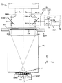
図8(A)には、投影光学系PLの光軸をZ軸とし、投影光学系PLの光軸AX上のベストフォーカス位置を原点とするXYZ座標系と、多点AF系(60A,60B)の計測領域MAの中心を原点とし、X軸,Y軸,Z軸にそれぞれ平行なX’軸、Y’軸、Z’軸から成るX’Y’Z’座標系とが示されている。前提として、Z’軸は、アライメント系ALGの検出視野の中心軸BXと一致しているものとする。図8(A)に示されるように、本実施形態では、両座標系の原点は当然に一致してはいない。また、投影光学系PLの光軸AX上のベストフォーカス位置と、多点AF系(60A,60B)の検出原点のZ位置にもずれ(ΔZ)が当然に存在する。 FIG. 8A shows an XYZ coordinate system in which the optical axis of the projection optical system PL is the Z axis and the best focus position on the optical axis AX of the projection optical system PL is the origin, and a multipoint AF system (60A, 60B). The X′Y′Z ′ coordinate system including the X ′ axis, the Y ′ axis, and the Z ′ axis, which is parallel to the X axis, the Y axis, and the Z axis, with the center of the measurement area MA in FIG. . As a premise, it is assumed that the Z ′ axis coincides with the center axis BX of the detection visual field of the alignment system ALG. As shown in FIG. 8A, in this embodiment, the origins of both coordinate systems do not naturally coincide. Further, there is naturally a deviation (ΔZ) between the best focus position on the optical axis AX of the projection optical system PL and the Z position of the detection origin of the multipoint AF system (60A, 60B).
また、図8(B)に示されるように、投影光学系PLのベストフォーカス位置は、投影光学系PLの収差等の影響により、有効露光フィールドである露光領域(露光領域IAとする)内の各箇所で微妙に異なる。すなわち、投影光学系PLの光軸AX上のベストフォーカス位置を原点としても、露光領域IA内の他の箇所では、投影光学系PLのベストフォーカス位置が必ずしもZ=0の平面内にあるとは限らない。そこで、本実施形態では、露光領域IA内に図8(B)に示されるX軸方向に例えば3.5mm間隔で、Y軸方向に例えば4mm間隔で配置された各計測点P11〜P37について空間像計測装置59などを用いてそれぞれベストフォーカス位置を計測し、複数の計測点P11〜P37のベストフォーカス位置で形成される最良結像面を求める。実際の走査露光では、このベストフォーカス面にウエハWの露光対象面を焦点深度内の範囲内で一致させるように、オープンなオートフォーカス・レベリング制御を行う。As shown in FIG. 8B, the best focus position of the projection optical system PL is within the exposure area (exposure area IA), which is an effective exposure field, due to the influence of the aberration of the projection optical system PL. It is slightly different in each part. That is, even if the best focus position on the optical axis AX of the projection optical system PL is used as the origin, the best focus position of the projection optical system PL is not necessarily in the plane of Z = 0 at other places in the exposure area IA. Not exclusively. Therefore, in the present embodiment, the measurement points P 11 to P 37 arranged in the exposure area IA at intervals of, for example, 3.5 mm in the X-axis direction and at intervals of, for example, 4 mm in the Y-axis direction shown in FIG. The best focus position is measured using the aerial
また、多点AF系(60A,60B)においては、計測点S11〜S88でのそれぞれのZ位置を複数のフォーカスセンサで独立して検出するので、各計測点のZ位置の検出原点には必ずずれが生じている。全てのフォーカスセンサのこの検出原点のずれを機械的にゼロとするのは困難である。そこで、本実施形態では、この検出原点のずれを、各計測点のオフセット成分として出力する。図8(C)には、各計測点S11〜S88でのオフセット成分D11〜D88の一例が模式的に示されている。このようなオフセット成分は、多点AF系(60A,60B)で検出されたウエハWの露光対象面の面形状に関する情報の誤差となるので、実際の面形状の検出に先立って、このオフセット成分D11〜D88を較正情報として検出しておく必要がある。Further, the multipoint AF system (60A, 60B) in, and detects independently each Z position at the measurement point S 11 to S 88 in a plurality of focus sensor, to detect the origin of the Z position of each measurement point There is always a gap. It is difficult to mechanically eliminate this detection origin deviation of all focus sensors. Therefore, in this embodiment, this detection origin deviation is output as an offset component of each measurement point. FIG. 8C schematically shows an example of offset components D 11 to D 88 at the measurement points S 11 to S 88 . Since such an offset component becomes an error in information regarding the surface shape of the exposure target surface of the wafer W detected by the multipoint AF system (60A, 60B), this offset component is detected prior to detection of the actual surface shape. it is necessary to detect the D 11 to D 88 as calibration information.
すなわち、本実施形態では、露光に先立って投影光学系PLの最良結像面と、多点AF系(60A,60B)の複数の計測点の検出原点によって形成される計測領域MAとのキャリブレーションを行う必要がある。 That is, in the present embodiment, calibration is performed between the best imaging plane of the projection optical system PL and the measurement area MA formed by the detection origins of a plurality of measurement points of the multipoint AF system (60A, 60B) prior to exposure. Need to do.
図9には、1枚のウエハに対し、露光を行う際の主制御装置20の処理アルゴリズムを示すフローチャートが示されている。図9に示されるように、まず、サブルーチン201では、投影光学系PLのベストフォーカス位置の検出を行う。すなわち、このサブルーチン201では、図10に示されるように、まず、ステップ301において、不図示のレチクルローダにより、レチクルステージRST上にレチクルR1をロードする。このレチクルR1は、図8(B)に示される露光領域IAの複数の計測点P11〜P37に対応する箇所に、計測マークPM(図3参照、ここではそれぞれ計測マークPMij(i=1〜3、j=1〜7)とする)が形成されたレチクルであるものとする。FIG. 9 is a flowchart showing a processing algorithm of the
次のステップ303では、レチクルR1上の中心に位置する中心マーク(図8(B)に示される計測点P24に対応する計測マークPM24)が、投影光学系PLの光軸上に一致するようにレチクルステージRSTを位置決めする。次のステップ304では、液体給排システム132による水Lqの給排水を開始する。これにより、先端レンズ91とスリット板90との間には水Lqが満たされるようになる。次いで、ステップ305では、計測マークの行番号を示すカウンタiの値(以下、「カウンタ値i」とする)を1に初期化し、次のステップ307では、計測マークの列番号を示すカウンタjの値(以下、「カウンタ値j」とする)を1に初期化する。そして、ステップ307では、計測マークPMijの部分にのみ照明光ILが照射されるように、照明系10を構成する可動レチクルブラインド12を駆動制御して照明領域を規定する。In the
次のステップ311では、スリット板90が、計測マークPMij(ここでは、計測マークPM11)の空間像をスリットスキャンが可能な走査開始位置に移動するようにウエハステージ駆動部WSCを介してウエハステージWSTを駆動する。次のステップ313では、照明光ILをレチクルR1に照射して、スリットスキャン方式により空間像計測装置59を用いて計測マークPMij(ここでは、計測マークPM11)の空間像計測を、ウエハステージWSTのZ位置を所定ステップピッチでずらしながら繰り返し行う。この各Z位置の空間像計測の際には、ウエハ干渉計18によって計測されるウエハステージWSTのZ位置に基づいて、ウエハステージ駆動部WSCを介してウエハステージWSTのZ位置が制御されている。また、スリット板90の傾き、すなわちウエハステージWSTの投影光学系PLの光軸AXに直交するXY平面に対する傾斜は、前述のように、ウエハ干渉計18、より正確にはウエハステージWSTのピッチング、ローリングをそれぞれ検出する測長軸を有する一対のY干渉計(ピッチング干渉計として機能する)、X干渉計(ローリング干渉計として機能する)の計測値に基づいて、所望の一定角度となるように(例えばピッチング、ローリングがともに零となるように)制御されている。そして、次のステップ315では、その空間像の計測結果に基づいて得られた計測マークPMijの空間像に関するコントラストカーブがピーク値を示すZ位置Zijを算出し、その位置Zijを評価点Pijにおけるベストフォーカス位置として内部メモリに記憶する。In the next step 311, the
なお、ウエハステージWSTのZ位置を変更した場合には、先端レンズ91とウエハWとの間隔も変わるため、液体給排システム132により、その間に保持される水Lqの量も適宜変更される。
Note that when the Z position of wafer stage WST is changed, the distance between
次のステップ317では、カウンタ値jを1インクリメントする(j←j+1)。そして、次のステップ319では、カウンタ値jが7を超えているか否かを判断する。ここでは、カウンタ値jが2であるので、判断は否定され、ステップ309に戻る。
In the
以降、カウンタ値jが7を越え、ステップ319において判断が肯定されるまで、ステップ309→ステップ311→ステップ313→ステップ315→ステップ317→ステップ319の処理、判断が繰り返し実行され、計測点P12〜P17における計測マークPM12〜PM17の空間像計測が複数のZ位置で行われ、各計測点におけるベストフォーカス位置Z11〜Z17が検出され、内部メモリに格納される。Thereafter, until the counter value j exceeds 7 and the determination in
カウンタ値jが7となり、ステップ319における判断が肯定されると、ステップ321に進む。ステップ321ではカウンタ値iが1だけインクリメントされる(i←i+1)。次のステップ323では、カウンタ値iが3を超えたか否かが判断される。ここでは、カウンタ値i=2なので、判断は否定され、ステップ307に戻る。
When the counter value j becomes 7 and the determination in
以降、カウンタ値i=4となってステップ323での判断が肯定されるまで、ステップ307→ステップ309→ステップ311→ステップ313→ステップ315→ステップ317→ステップ319の処理、判断が繰り返し実行され、計測点P21〜P27における計測マークPM21〜PM27の空間像計測が複数のZ位置で行われ、各計測点におけるベストフォーカス位置Z21〜Z27が検出されて内部メモリに格納される。そして、さらにもう1回、ステップ307→ステップ309→ステップ311→ステップ313→ステップ315→ステップ317→ステップ319の処理、判断が繰り返し実行され、計測点P31〜P37における計測マークPM31〜PM37の空間像計測が複数のZ位置で行われ、各計測点におけるベストフォーカス位置Z31〜Z37が検出され、内部メモリに格納される。Thereafter, until the counter value i = 4 and the determination in
カウンタ値iが4になると、ステップ323での判断が肯定され、ステップ325に進む。ステップ325では、上述のようにして得られた各ベストフォーカス位置Z11、Z12、……、Z37に基づいて、所定の統計的処理を行うことにより、投影光学系PLの像面の近似平面(及び像面形状)を算出する。このとき、この像面形状とは別に像面湾曲を算出することも可能である。投影光学系PLの像面、すなわち最良結像面は、光軸からの距離が異なる無数の点(すなわち、いわゆる像の高さが異なる無数の点)におけるベストフォーカス位置の集合から成る面であるから、このような手法により、像面形状及びその近似平面を容易にかつ正確に求めることができる。When the counter value i becomes 4, the determination in
次のステップ327では、RA検出系12A,12Bの焦点合わせをする。まず、図6に示されるように、ウエハステージWST上の基準マーク板FMの第1基準マークWM1,WM2が、RA検出系12A,12Bの検出視野に入るように、ウエハステージWST上を投影光学系PLの直下に移動させる。このとき、ウエハステージWSTは、基準マーク板FMが、投影光学系PLの最良結像面に位置するようにオートフォーカス・レベリング制御されているものとする。なお、ウエハステージWSTの上面は、ウエハWを含み、ほぼ完全な平面となっているため、この移動の際には、液体給排システム132により水の給排を停止させる必要はない。In the
さらに、図6に示されるRA検出系12A,12Bの可動部33A,33Bを、不図示の駆動装置を介してレチクルR1上に移動させ、レチクルR1及び投影光学系PLを介して、ウエハステージWST上の基準マーク板FMに形成された一対の第1基準マークWM1,WM2を照明光IL1,IL2により照明する。これにより、それら第1基準マークWM1,WM2部分からの反射光束が投影光学系PLを介してレチクルR1のパターン面のパターン領域PAを挟むX軸方向の両側の位置に戻り、レチクルR1のパターン面に第1基準マークWM1,WM2の投影像が結像される。なお、このとき、レチクルR1上のRAマークは、いずれもRA検出系12A,12Bの視野外、視野内のいずれにあっても良い。これはRAマーク、第1基準マークWM1,WM2ともに既知の構造であり、信号処理の過程で容易に判別可能であることによる。そして、RA検出系12A,12Bを構成するそれぞれの結像光学系35内の合焦状態調整用レンズ39を駆動装置41を介してその光軸方向に沿って所定範囲内で所定ピッチであるいは連続的に駆動する。そして、この駆動中にRA検出系(12A,12B)から出力される検出信号、すなわち第1基準マークWM1,WM2の像強度(光強度)信号をモニタし、そのモニタ結果に基づいてそれぞれの結像光学系35が合焦状態となる位置を見つけ、その位置に合焦状態調整用レンズ39の光軸方向位置を設定して、RA検出系12A,12Bを構成するそれぞれの結像光学系35を合焦させる。上記の合焦状態の判断は、一例として光強度信号のコントラストがピークとなる位置を見つけ、その位置を合焦位置とすることによって行うことができる。勿論、この他の手法によって、合焦状態を判断しても良い。これにより、RA検出系(12A,12B)のベストフォーカス位置は、投影光学系PLの最良結像面に一致するようになる。Further, the
次のステップ329では、液体給排システム132により水の給排を停止される。これにより、先端レンズ91の下方の水が除去される。ステップ329が終了すると、図9のステップ203に進む。
In the
次のステップ203では、前述の如く基準平面板を兼ねるスリット板90がアライメント系ALGの下方(すなわち多点AF系の計測領域MA)に位置するように、ウエハステージ駆動部WSCを介してウエハステージWSTを移動させる。このとき、スリット板90の傾き、すなわちウエハステージWSTの投影光学系PLの光軸AXに直交するXY平面に対する傾斜は、ウエハ干渉計18、より正確には、ウエハステージWSTのピッチング、ローリングをそれぞれ検出する測長軸を有する一対のY干渉計(ピッチング干渉計として機能する)、X干渉計(ローリング干渉計として機能する)の計測値に基づいて、所望の一定角度となるように(例えばピッチング、ローリングがともに零となるように)制御されている。さらに、主制御装置20は、多点AF系(60A,60B)により計測される計測点S11〜S88(この場合スリット板90上の各計測点)の計測結果が1つでも計測範囲からはずれ、飽和することのないような位置に、ウエハステージWSTのZ位置を調整する。In the
次のステップ205では、このときの各計測点S11〜S88の計測結果を取得し、この計測結果を図8(C)で示されるような計測点S11〜S88のオフセット成分D11〜D88として内部メモリに格納するとともに、このときのウエハステージWSTのZ位置を併せて内部メモリに格納する。In the
なお、ここで、ウエハステージWSTのZ位置を調整しても、計測結果が飽和する計測点がなくならない場合には、多点AF系(60A,60B)を構成する調整部材、例えば平行平板ガラスの回転量を調整するようにしても良い。 Here, when the Z position of wafer stage WST is adjusted and the measurement points at which the measurement result is saturated do not disappear, an adjustment member that constitutes the multipoint AF system (60A, 60B), for example, parallel flat glass The amount of rotation may be adjusted.
次のステップ207では、レチクル交換を行う。これにより、レチクルステージRSTに保持されたレチクルR1が不図示のレチクルアンローダによりアンロードされ、実際の露光に用いられるレチクルRが不図示のレチクルローダによりロードされる。
In the
次のステップ209では、レチクルアライメント系(12A,12B)及び基準マーク板FM等を用いて、通常のスキャニング・ステッパと同様の手順で、レチクルアライメント及びベースライン計測などの準備作業を行う。なお、準備作業のうち、レチクルアライメントにおいては、液体給排システム132により先端レンズ91と基準マーク板FMとの間に水Lqが供給された状態で行う。レチクルアライメント後は水の給排を停止させる。
In the
次のステップ211では、ウエハステージWSTをローディング位置に移動させ、不図示のウエハローダによりウエハステージWST上にウエハWをロードする。次のステップ213では、サーチアライメントを行う。このサーチアライメントに関しては、例えば特開平2−272305号公報及びこれに対応する米国特許第5,151,750号などに詳細に開示されている方法と同様な方法が用いられる。本国際出願で指定した指定国(又は選択した選択国)の国内法令が許す限りにおいて、上記公報及び対応する米国特許における開示を援用して本明細書の記載の一部とする。
In the
次のステップ215では、ウエハステージWSTをアライメント系ALGの直下に移動させ、ウエハステージWST上のウエハWに対してウエハアライメント(ファインアライメント)を行う。ここでは、一例として、例えば特開昭61−44429号公報及びこれに対応する米国特許第4,780,617号などに詳細に開示されるEGA(エンハンスト・グローバル・アライメント)方式のウエハアライメントを行うものとする。なお、本国際出願で指定した指定国(又は選択した選択国)の国内法令が許す限りにおいて、上記公報及び対応米国特許における開示を援用して本明細書の記載の一部とする。
In the
このウエハアライメントでは、図11(A)に実線枠で示されるウエハW上の各ショット領域SAのうち、例えば図中になし地模様を付して示されるような14個のショット領域SAをサンプルショット領域として選択するものとする。ここでは、サンプルショット領域に付設されたウエハアライメントマークをアライメント系ALGにより検出して、そのマークのXY平面内の位置情報を検出し、その検出結果からウエハW上のショット領域の配列座標を後述するステップ217で算出する。
In this wafer alignment, for example, 14 shot areas SA as shown with a background pattern in the drawing are sampled among the shot areas SA on the wafer W indicated by the solid frame in FIG. The shot area is selected. Here, the wafer alignment mark attached to the sample shot area is detected by the alignment system ALG, the position information of the mark in the XY plane is detected, and the arrangement coordinates of the shot area on the wafer W are described later from the detection result. In
なお、このウエハアライメントでは、ウエハステージWSTをXY平面内に移動させて、各サンプルショット領域に付設されたウエハアライメントマークをアライメント系ALGの検出視野に順次移動させたうえで、そのウエハアライメントマークを検出している。言い換えれば、全サンプルショット領域に付設されたウエハアライメントマークを検出する際には、アライメント系ALGの検出視野が所定の経路で14個のサンプルショットを順次移動するようになる。図11(A)では、アライメント系ALGの検出視野が各サンプルショット領域の中心を捉えているときの多点AF系の計測領域MAが点線枠で示されている。このように、アライメント系ALGの検出視野が所定の経路で14個のサンプルショットを順次移動すると、多点AF系(60A,60B)の計測領域MAがウエハWのほぼ全面を網羅するようになる。
In this wafer alignment, the wafer stage WST is moved in the XY plane, and the wafer alignment mark attached to each sample shot area is sequentially moved to the detection field of the alignment system ALG, and then the wafer alignment mark is moved. Detected. In other words, when detecting wafer alignment marks attached to all sample shot areas, the detection field of alignment system ALG sequentially
そこで、ステップ215においては、アライメント系ALGによりサンプルショット領域に付設されたウエハアライメントマークを検出するとともに、多点AF系(60A,60B)により、ウエハWの表面のZ位置(面位置)計測も合わせて行う。すなわち、アライメントALGの検出視野が各サンプルショット付近に移動する毎に、図11の点線枠で示されるような多点AF系の計測領域内の計測点S11〜S88のZ位置が計測される。これにより、ほぼ全域のウエハWの露光対象面のZ位置が得られるようになる。また、この多点AF系(60A,60B)の計測点S11〜S88におけるZ位置の計測の際には、そのときのウエハステージWSTのXY平面内位置及びZ位置も、ウエハ干渉計18の計測により取得しておく。このときのZ位置と、投影光学系PLの原点P24におけるベストフォーカス位置との差が図8(A)に示されるΔZとなる。Therefore, in
なお、多点AF系(60A,60B)の計測点S11〜S88の検出原点は、前述のようにずれがあるため、各計測点におけるZ位置の計測値から上記ステップ205で求めたオフセット成分D11〜D88をキャンセルしておく必要がある。Since the detection origins of the measurement points S 11 to S 88 of the multi-point AF system (60A, 60B) are deviated as described above, the offset obtained in
このように、ステップ215におけるウエハアライメントでは、ウエハアライメントマークの計測とともに、多点AF系(60A,60B)によりウエハWの露光対象面のZ位置が計測される。このZ位置と、そのZ位置が計測されたときのウエハ干渉計18の計測値(ウエハステージWSTのXY平面内の位置情報及びZ軸方向の位置情報)から、ウエハWの露光対象面の面形状に関する情報を取得することができる。以下では、この情報をZマップと呼び、このZマップを取得する処理をZマッピングと呼ぶものとする。なお、このZマップは、XY平面に関し離散的なデータであるので、所定の補間演算又は統計演算等により、ウエハWの露光対象面の面形状に関する情報を表す連続値関数を作成するようにしても良い。図11(B)には、図11(A)のA−A’断面におけるZマップに基づいて作成された連続値関数の一例が示されている。図中のZaは、このZマップにおけるウエハWの露光対象面の平均Z位置を示している。
Thus, in the wafer alignment in
次のステップ217では、上記ステップ215で検出されたEGA方式のウエハアライメントの結果に基づいてウエハW上のショット領域の配列座標を計算する。そして、次のステップ219では、この配列座標と、Zマップと、上記ステップ209におけるベースライン計測結果に基づいて、走査露光中のウエハステージWSTのXYZ座標系の6自由度の位置指令プロファイルを作成する。このとき、上記ステップ215で作成されたZマップに基づいてオートフォーカス・レベリング制御に寄与する位置指令プロファイルを作成する際には、図8(A)に示されるようなZ軸とZ’軸とのずれΔZを考慮する必要があることは勿論である。
In the
次のステップ221では、ウエハWの複数のショット領域に対する走査露光を行う。具体的には、上記ステップ219で作成したウエハステージWSTのXYZ座標系の6自由度の位置指令プロファイルに基づいて、第1番目のショット領域(ファーストショット)の露光のための加速開始位置にウエハW(ウエハステージWST)を移動させ、これと同時に、レチクルR(レチクルステージRST)を加速開始位置へ移動させる。そして、液体給排システム132により先端レンズ91とウエハWとの間に対し水Lqの給排を開始する。そして、上記ステップ219で作成された位置指令プロファイルに基づいて、ウエハW(ウエハステージWST)とレチクルR(レチクルステージRST)とのY軸方向の相対走査(同期移動)を開始し、ウエハW上のファーストショットに対して走査露光を行う。これにより、レチクルRの回路パターンが投影光学系PLを介してウエハW上のファーストショットに対して逐次転写される。
In the
上記の走査露光中、ウエハWの表面上の露光領域IAが投影光学系PLの最良結像面とを実質的に一致させる(結像面の焦点深度の範囲内に収まる)ようにするために、ウエハ干渉計18で計測されるウエハステージWSTのXY平面位置及びZ位置と、ステップ215において検出されたZマップとに基づいて、ウエハステージ駆動部WSCを介してウエハステージWSTをZ軸方向、θx方向、θz方向に駆動し、ウエハWに対するオープンループのフォーカス・レベリング制御が実現される。
In order to make the exposure area IA on the surface of the wafer W substantially coincide with the best imaging plane of the projection optical system PL during the above scanning exposure (contains within the range of the focal depth of the imaging plane). Based on the XY plane position and Z position of wafer stage WST measured by
そして、ファーストショットに対する走査露光動作が終了すると、主制御装置20は、ウエハW上の第2番目のショット領域(セカンドショット)の露光のための加速開始位置にウエハWが位置するようにウエハステージWSTを移動させる。このとき、完全交互スキャン方式が採用されているので、レチクルステージRSTは、前ショット領域に対する走査露光のための一連の動作が終了した時点で次ショット領域に対する露光を行うための加速開始位置に移動している。
When the scanning exposure operation for the first shot is completed,
主制御装置20は、その後レチクルステージRSTとウエハステージWSTの相対走査を開始し、前述と同様の走査露光を行い、レチクルRのパターンを投影光学系PLを介してウエハW上のセカンドショットに逐次転写し、その転写中、前述と同様のウエハWに対するオープンループのフォーカス・レベリング制御を実行する。
以後、上記と同様のウエハステージWSTの移動(ショット間ステップ動作)及び走査露光が繰り返し行われ、ウエハW上の第3ショット領域以降のショット領域に対して、レチクルRのパターンがそれぞれ転写される。 Thereafter, the movement of wafer stage WST (step operation between shots) and scanning exposure similar to those described above are repeated, and the pattern of reticle R is transferred to the shot areas on and after third shot area on wafer W, respectively. .
このようにしてウエハW上の全てのショット領域に対する走査露光が終了した後、液体給排システム132による水Lqの給排が停止され、ステップ223において、ウエハステージWSTをアンロード位置に移動させ、ウエハWを不図示のウエハアンローダによりアンロードする。ステップ223終了後は、処理を終了する。
After the scanning exposure for all shot areas on the wafer W is completed in this way, the supply / discharge of the water Lq by the liquid supply /
なお、本実施形態では、投影光学系PLのベストフォーカス位置を検出してから、多点AF系(60A,60B)のオフセット成分を検出したが、これは逆であっても良い。また、サーチアライメントは行わなくても良い。また、ファインアライメントにおける、サンプルショット数は14個には限らず、例えば8個でも良い。この場合には、アライメント系ALGのアライメントマークの検出に関わらず、図11(A)に示されるような領域MAでのウエハWの面位置検出を行うようにする。 In the present embodiment, the offset component of the multipoint AF system (60A, 60B) is detected after the best focus position of the projection optical system PL is detected, but this may be reversed. Search alignment may not be performed. Further, the number of sample shots in fine alignment is not limited to 14, but may be, for example, 8. In this case, the surface position of the wafer W in the area MA as shown in FIG. 11A is detected regardless of the detection of the alignment mark of the alignment system ALG.
また、ウエハWがベアウエハである場合には、ステップ213のサーチアライメント及びステップ215のファインアライメント(さらにはステップ217の配列座標計算)は行われないが、多点AF系によるウエハWの面位置検出は行う必要がある。
If the wafer W is a bare wafer, the search alignment in
これまでの説明から明らかなように、本実施形態の露光装置100では、ウエハステージWSTによってステージの少なくとも一部が構成され、ウエハ干渉計18によって、第1位置検出装置及び第2位置検出装置の少なくとも一部が構成される。また、多点AF系(60A,60B)及び主制御装置20の一部を含んで面形状検出系が構成され、主制御装置20の一部を含んで調整装置が構成されている。また、主制御装置20の一部を含んで計測装置が構成されている。また、多点AF系(60A,60B)を含んで焦点位置検出系が構成されている。また、RA検出系(12A,12B)を含んで検出機構が構成されている。
As is apparent from the above description, in the
すなわち、主制御装置20のCPUが行う、ステップ215(図9)の処理によって面形状検出系の一部の機能が実現され、ステップ205、ステップ221(図9)等の処理によって調整装置の機能が実現され、サブルーチン201(図9、図10)の処理によって計測装置の機能が実現されている。また、本実施形態では、主制御装置20の機能を、1つのCPUで実現したが、複数のCPUで実現しても良い。
That is, a part of the function of the surface shape detection system is realized by the process of step 215 (FIG. 9) performed by the CPU of the
以上詳細に説明したように、本実施形態の露光装置100によれば、投影露光に先立って、ウエハステージWSTに保持されたウエハWの露光対象面の面形状に関する情報(Zマップ)を面形状検出系(多点AF系(60A,60B),主制御装置20の一部)により検出しておき、投影露光が行われる際には、その面形状検出系により検出された露光対象面の面形状に関する情報(Zマップ)などに基づいて主制御装置20によりウエハステージWST上のウエハWの面位置を調整するので、投影露光の際に、投影光学系PLの光軸AXの方向に関するウエハWの位置を、リアルタイムに検出せずとも、走査露光中のウエハW上の露光領域IAを投影光学系PLの最良結像面の焦点深度の範囲内に位置させることができ、大開口数の投影光学系の下での高精度な露光を実現することができる。
As described above in detail, according to the
また、本実施形態では、主制御装置20は、投影光学系PLのベストフォーカス位置を計測して最良結像面を検出し、その最良結像面を基準として、ウエハWの露光対象面の面位置を調整するが、投影光学系PLの最良結像面がXY平面にほぼ平行であることが保障されていれば、投影光学系PLの最良結像面を求める必要はなく、有効露光フィールド内のいずれか1つ(例えば光軸上)の計測点におけるベストフォーカス位置を求めるだけでも良い。また、計測点P11〜P37の間隔及び計測点数は、上記実施形態のものには限られない。In the present embodiment, the
また、本実施形態では、投影光学系PLのベストフォーカス位置を空間像計測装置59による空間像計測により求めたが、これには限られず、ベストフォーカス位置の検出方法はどのようなものであっても良い。例えば、複数のZ位置で実際にウエハWに対する所定パターンの焼付けを行い、その焼付け結果が最も良好であったZ位置をベストフォーカス位置として決定するようにしても良い。この場合には、露光装置が空間像計測装置を備える必要はない。
In this embodiment, the best focus position of the projection optical system PL is obtained by aerial image measurement by the aerial
また、上記実施形態では、多点AF系(60A,60B)の計測領域MAの中心が、アライメント系ALGの検出視野の中心と一致するようにしたが、必ずしもその必要はない。アライメント系ALGによるウエハアライメントマークの検出と、多点AF系(60A,60B)によるウエハWの面位置の検出とを同時に行わない場合には、両者を別々に配置するようにしても良い。ただし、両者を上記実施形態のように配置すれば、ウエハアライメントマークの検出と、ウエハWの面位置の検出とを同時に行えるので、スループット的に有利である。 In the above embodiment, the center of the measurement area MA of the multipoint AF system (60A, 60B) is made to coincide with the center of the detection visual field of the alignment system ALG, but this is not always necessary. When the detection of the wafer alignment mark by the alignment system ALG and the detection of the surface position of the wafer W by the multipoint AF system (60A, 60B) are not performed at the same time, they may be arranged separately. However, if both are arranged as in the above embodiment, detection of the wafer alignment mark and detection of the surface position of the wafer W can be performed simultaneously, which is advantageous in terms of throughput.
また、上記実施形態では、多点AF系(60A,60B)の計測点の数は8×8=64点であったが、これには限られないことは勿論である。また、計測領域MAの大きさや、各計測点のサイズや向きも上記実施形態のものには限定されない。例えばこの計測点の間隔を、投影光学系PLのベストフォーカス位置の計測点の間隔(X:4mm、Y:3.5mm)と同じにしても良い。また、上記実施形態では、ウエハWの面位置を検出する検出系が多点AF系(60A,60B)であったが、その必要はない。例えば、ウエハWの1点のみのZ位置を検出する検出系であっても良い。この場合には、その検出系のオフセット成分というものは観念できないので、上記ステップ205におけるようなオフセット成分を検出する必要はなく、図8(A)に示されるようなΔZだけを検出すれば良い。
In the above embodiment, the number of measurement points of the multi-point AF system (60A, 60B) is 8 × 8 = 64, but it is needless to say that the number is not limited to this. Further, the size of the measurement area MA and the size and orientation of each measurement point are not limited to those of the above embodiment. For example, the interval between the measurement points may be the same as the interval between the measurement points at the best focus position of the projection optical system PL (X: 4 mm, Y: 3.5 mm). In the above embodiment, the detection system for detecting the surface position of the wafer W is the multipoint AF system (60A, 60B), but this is not necessary. For example, a detection system that detects the Z position of only one point on the wafer W may be used. In this case, since the offset component of the detection system cannot be considered, it is not necessary to detect the offset component as in
また、上記実施形態では、多点AF系(60A,60B)を用いてウエハWの露光対象面の面形状に関する情報(Zマップ)を検出する際に、そのときのウエハステージWSTのZ位置をウエハ干渉計18によって計測し、その計測結果に基づいて面形状が検出されたウエハWの面を、投影光学系PLの最良結像面とに焦点深度の範囲内で一致させるようにした。このように、図1に示される露光装置100のように、投影光学系PLの下方からアライメント系ALGの下方までの広いXY平面に平行な領域を網羅するZ干渉計を備えていれば、ウエハステージWSTがどのような位置にあっても、そのZ位置は常に同一ウエハ干渉計18によって検出され、そのZ位置を絶対Z位置として用いることができる。
In the above embodiment, when detecting information (Z map) on the surface shape of the exposure target surface of the wafer W using the multipoint AF system (60A, 60B), the Z position of the wafer stage WST at that time is detected. The surface of the wafer W, which was measured by the
しかしながら、露光装置の構成は、上記実施形態のものには限られない。例えば図1に示されるようなウエハ干渉計18を備えておらず、例えば投影光学系PLの下方にあるウエハステージWSTのZ位置を計測する干渉計と、アライメント系ALGの下方にあるウエハステージWSTのZ位置を計測する干渉計とが、それぞれ独立した干渉計である露光装置やZ位置を計測する干渉計を備えていない露光装置では、アライメント位置にあるウエハWの露光対象面の面形状を検出したときのZ位置を、露光時には参照することができなくなる。
However, the configuration of the exposure apparatus is not limited to that of the above embodiment. For example, an interferometer that does not include
このような場合には、RA検出系(12A,12B)を用いてZ位置の位置合わせを行うようにしても良い。以下では、その位置合わせの方法について説明する。 In such a case, the Z position may be aligned using the RA detection system (12A, 12B). Hereinafter, the alignment method will be described.
例えば、上記ステップ215におけるZマッピングの際に、ウエハWの露光対象面の面形状とともに、基準マーク板FMの面位置も多点AF系(60A,60B)を使って計測し、内部メモリに記憶しておく。そして、ウエハステージWST上のウエハWに対し露光を行うため、ウエハステージWSTを投影光学系PLの下方に移動させた場合に、RA検出系(12A,12B)により、基準マーク板FM上の第1基準マークWM1,WM2を検出させる。主制御装置20は、ウエハステージWSTをZ軸方向に駆動して、RA検出系(12A,12B)によって、第1基準マークに対応する光強度信号のコントラストがピークとなるZ位置を見つける。このとき、RA検出系(12A,12B)では、上記ステップ327における合焦動作がすでに行われており、基準マーク板FMの表面位置が、投影光学系PLの最良結像面に合致するように設定されているものとすれば、この位置が投影光学系のベストフォーカス位置に対応していることになる。したがって、このようにすれば、基準マーク板FMの面位置とウエハWの露光対象面の面位置との相対位置関係から、現在のウエハWの露光対象面のZ位置を把握することができるので、上記実施形態と同様に、走査露光中に、ウエハWの露光対象面と投影光学系PLの最良結像面とを焦点深度の範囲内で一致させることができるようになる。For example, at the time of Z mapping in
なお、上記実施形態のように、投影光学系PLの最良結像面(ベストフォーカス位置)と、RA検出系(12A,12B)のベストフォーカス位置などを必ずしも一致させる必要はない。両者のZ軸方向のずれが既知であれば良い。RA検出系(12A,12B)により基準マーク板FMを検出させることにより、RA検出系(12A,12B)のベストフォーカス位置に基準マーク板FMを位置させることができれば、その時点での基準マーク板FMと投影光学系PLの最良結像面との相対位置関係がわかるので、投影光学系PLの最良結像面とウエハWの露光対象面とを焦点深度の範囲内で、一致させることは可能だからである。したがって、上記実施形態のようにRA検出系には必ずしも合焦装置が備えられている必要はない。 Note that, as in the above-described embodiment, the best imaging plane (best focus position) of the projection optical system PL and the best focus position of the RA detection system (12A, 12B) are not necessarily matched. It is only necessary that the deviation in the Z-axis direction is known. If the reference mark plate FM can be positioned at the best focus position of the RA detection system (12A, 12B) by detecting the reference mark plate FM by the RA detection system (12A, 12B), the reference mark plate at that time Since the relative positional relationship between the FM and the best imaging plane of the projection optical system PL is known, it is possible to match the best imaging plane of the projection optical system PL and the exposure target plane of the wafer W within the depth of focus range. That's why. Therefore, the RA detection system is not necessarily provided with the focusing device as in the above embodiment.
ただし、この場合には、投影光学系PLの最良結像面と、RA検出系のベストフォーカス位置との位置関係のキャリブレーションを予め行っておく必要がある。投影光学系PLの最良結像面については、上記実施形態と同様の方法で求めることができる。一方、RA検出系のベストフォーカス位置については、やはり基準マーク板FM上の第1基準マークの検出結果のZ軸方向に関するコントラストカーブなどから求めることができる。 In this case, however, calibration of the positional relationship between the best imaging plane of the projection optical system PL and the best focus position of the RA detection system needs to be performed in advance. The best imaging plane of the projection optical system PL can be obtained by the same method as in the above embodiment. On the other hand, the best focus position of the RA detection system can also be obtained from the contrast curve in the Z-axis direction of the detection result of the first reference mark on the reference mark plate FM.
以上述べたように、ウエハWの露光対象面の面形状を検出する際には、ウエハWの面の絶対Z位置を求めるだけでも良いが、ウエハステージWST上の基準面に対するウエハWの面の相対Z位置を求めるだけでも、投影光学系PLの最良結像面にウエハWの露光面を一致させることができる。 As described above, when detecting the surface shape of the exposure target surface of the wafer W, it is only necessary to obtain the absolute Z position of the surface of the wafer W, but the surface of the wafer W relative to the reference surface on the wafer stage WST may be obtained. Only by obtaining the relative Z position, the exposure surface of the wafer W can be made to coincide with the best imaging plane of the projection optical system PL.
なお、基準マーク板FMのZ位置の検出には、必ずしもRA検出系を用いる必要はない。要は、基準マーク板FMの表面と投影光学系PLの最良結像面との関係が求められればよく、投影光学系PLを介して基準マーク板FMの面位置を検出可能な別の検出系を用いても良いし、投影光学系PLを介さずに、例えば水なしで静電容量センサなど非光学的な検出系を用いて基準マーク板FMの面位置を検出できるようにしても良い。また、基準マーク板FMを使わずに、別途基準平面をウエハステージWST上に配置して使用するようにしても良い。 Note that it is not always necessary to use the RA detection system to detect the Z position of the reference mark plate FM. In short, it is only necessary to obtain the relationship between the surface of the reference mark plate FM and the best imaging plane of the projection optical system PL, and another detection system capable of detecting the surface position of the reference mark plate FM via the projection optical system PL. Alternatively, the surface position of the reference mark plate FM may be detected without using the projection optical system PL and using a non-optical detection system such as a capacitance sensor without water, for example. Further, a reference plane may be separately arranged on wafer stage WST without using reference mark plate FM.
また、上記実施形態では、特開平6−283403号公報に開示された多点AF系と同様の構成を有し、アライメント系ALGの検出視野中心と中心が一致する計測領域を有する多点AF系(60A,60B)を用いてウエハWの露光対象面の面形状に関する情報を検出したが、これには限られない。例えば図12(A)、図12(B)に示されるような面形状検出装置を用いても良い。図12(A)に示されるように、この面形状検出装置は、ウエハステージWST上のウエハWに対し、少なくともウエハWの直径より長いライン状のビームを斜入射させる照射系75Aと、照射系75Aにより照射されたビームの反射光を受光する例えば1次元CCDセンサなどの受光系75Bを含んで構成されている。図12(B)に示されるように、この照射系75Aと受光系75Bとは、投影光学系PLとアライメント系ALGとの間に、そのライン状の照射領域SLが位置するように配置されている。
In the above embodiment, the multipoint AF system has the same configuration as the multipoint AF system disclosed in Japanese Patent Laid-Open No. Hei 6-283403, and has a measurement region whose center coincides with the center of the detection field of the alignment system ALG. Information on the surface shape of the exposure target surface of the wafer W is detected using (60A, 60B), but is not limited thereto. For example, a surface shape detection apparatus as shown in FIGS. 12A and 12B may be used. As shown in FIG. 12A, the surface shape detection apparatus includes an
照射系75Aから照射されるライン状のビームは、実際には、互いに平行な複数の点状(またはスリット状)レーザ光が、一方向に並ぶことによって形成されたビームであり、この照射領域SLは、図12(C)に示されるように、実際には、複数の点状のビームの照射領域S1〜Snの集合となっている。したがって、上記実施形態の多点AF系(60A,60B)の各計測点でのZ位置の検出原理と同じ原理で、この照射領域S1〜Snを計測点S1〜Snとし、受光系75Bにおける反射光の受光位置の基準位置からの位置ずれ量を計測すれば、計測点S1〜SnのそれぞれのウエハWのZ位置を検出することができる。The linear beam irradiated from the
受光系75Bでの計測結果は、主制御装置20に送られている。主制御装置20では、この計測結果、すなわち受光系75Bにおける反射光の受光位置の基準位置からの位置ずれ量に基づいて、ウエハWの露光対象面の面形状に関する情報を検出する。
The measurement result in the
照射領域SLを図12(B)に示されるように、計測点S1〜Snの列を、X軸およびY軸と交差するように配置したのは、例えばアライメント系ALGによるウエハアライメントマークの計測を終了した後に露光を行うため、ウエハステージWSTが、アライメント系ALGの下方(点線で示される位置)から投影光学系PLの下方(実線で示される位置)に移動する際に、ウエハステージWST上のウエハWが、この照射領域SLを通過するようになっているためである。この配置により、アライメントと露光との間にウエハステージWSTが移動する間に、この照射領域SLに対し、ウエハWが相対走査されるようになる。したがって、この相対走査の間(ウエハWが、照射領域SLを通過している間)、計測点S1〜Snの計測結果を所定のサンプリング間隔で検出していけば、その検出結果がウエハWの露光対象面全体の面形状を検出することができる。このように、アライメント位置(アライメント系ALGでウエハW上のアライメントマークの検出が行われる計測位置)から露光位置(投影光学系PLを使ってウエハ(基板)Wの露光が行われる露光位置)までウエハステージWSTを移動させる間にウエハWの面形状を検出すれば、スループットを低下させることなく、ウエハWの露光対象面の面形状を検出することができるようになる。もちろん、アライメント位置から露光位置へのウエハステージWSTを移動させる間に限らず、例えば次に露光されるウエハWをウエハステージWST上に搭載するウエハローディング位置から上記アライメント位置へウエハステージWSTを移動する間に、すなわちアライメント系ALGによるウエハW上のアライメントマークの検出を行う前に、ウエハWの露光対象面の面形状を検出するようにしても良い。The irradiation area SL as shown in FIG. 12 (B), a column of measurement points S 1 to S n, was arranged so as to intersect the X and Y axes, for example, the wafer alignment marks by alignment system ALG Since exposure is performed after the measurement is finished, wafer stage WST is moved when wafer stage WST moves from below alignment system ALG (position indicated by a dotted line) to below projection optical system PL (position indicated by a solid line). This is because the upper wafer W passes through the irradiation area SL. With this arrangement, the wafer W is relatively scanned with respect to the irradiation area SL while the wafer stage WST moves between alignment and exposure. Therefore, during the relative scanning (while the wafer W passes through the irradiation area SL), if the measurement results of the measurement points S 1 to Sn are detected at a predetermined sampling interval, the detection result is the wafer. The surface shape of the entire exposure target surface of W can be detected. In this way, from the alignment position (measurement position where the alignment mark ALG is detected on the wafer W) to the exposure position (exposure position where the wafer (substrate) W is exposed using the projection optical system PL). If the surface shape of the wafer W is detected while the wafer stage WST is moved, the surface shape of the exposure target surface of the wafer W can be detected without reducing the throughput. Of course, not only during the movement of wafer stage WST from the alignment position to the exposure position, but, for example, wafer stage WST is moved from the wafer loading position where wafer W to be exposed next is mounted on wafer stage WST to the alignment position. In the meantime, that is, before the alignment mark on the wafer W is detected by the alignment system ALG, the surface shape of the exposure target surface of the wafer W may be detected.
なお、計測点S1〜Snの列の配置は、上述の例に限られず、X軸またはY軸と平行に配置しても良い。また、計測点S1〜Snを用いたウエハWの面形状の計測は、ウエハアライメントマークの計測動作とウエハ露光動作との間に限らず、例えばウエハアライメントマークの計測前に行うようにしても良い。要は、ウエハWの露光前に、照射領域SLに対してウエハWが相対走査されれば良い。The arrangement of the rows of the measurement points S 1 to S n is not limited to the above example, it may be arranged parallel to the X-axis or Y-axis. Also, measurement of the surface shape of the wafer W with measurement points S 1 to S n is not limited to between the measurement operation and the wafer exposure operation of the wafer alignment mark, for example, as carried out before the measurement of the wafer alignment marks Also good. In short, the wafer W may be scanned relative to the irradiation area SL before the exposure of the wafer W.
また、図13に示されるような構成を有する面形状検出装置を備えるようにしても良い。図13に示される面形状検出装置は、斜入射する照明光を出射する不図示の光源と、該光源とウエハステージWST上のウエハWとの間に挿入された半透明参照面を有する平行平板96と、受光装置95とを含んで構成されている。光源から照射され平行平板96に入射する照明光の光束の大きさは、少なくともウエハWの面積よりも十分に大きくなるように設定されている。図13に示されるように、実線で示される入射光の一部は、平行平板96を通過してウエハWの露光対象面に至り、その面で反射され、平行平板96に再度入射する。再度入射した反射光は、その入射位置の半透明参照面で反射した点線で示される入射光と重なり、2次元CCDカメラ等の受光装置95においてそれらの干渉縞が形成されるようになる。したがって、その干渉縞の検出結果から、ウエハWの露光対象面の面形状を検出することができる。通常のフィゾー干渉計においては、被検反射物体に対する入射光波の入射角を垂直に規定しているが、図13に示されるような干渉計による面形状検出装置にあっては、入射光波がウエハWの露光対象面に対し斜入射するように設定されている。このようにすれば、ウエハW上に形成された回路パターン等の影響を軽減することができるとともに、縞感度を向上させることもできるようになる。
Moreover, you may make it provide the surface shape detection apparatus which has a structure as shown in FIG. The surface shape detection apparatus shown in FIG. 13 includes a parallel plate having a light source (not shown) that emits obliquely incident illumination light and a translucent reference surface inserted between the light source and wafer W on wafer stage WST. 96 and a
もっとも、ウエハWの露光対象面の面形状を測定するための干渉計の構成は図13に示されるようなものには限られない。上述のような入射光波が被検面に対して垂直に入射するフィゾー干渉計やトワイマン−グリーン干渉計のようなものであっても良い。また、特開平4−221704号公報や特開2001−4336号公報に開示されるような斜入射干渉計であっても良い。 However, the configuration of the interferometer for measuring the surface shape of the exposure target surface of the wafer W is not limited to that shown in FIG. It may be a Fizeau interferometer or a Twiman-Green interferometer in which the incident light wave is incident perpendicular to the surface to be measured. Further, it may be an oblique incidence interferometer as disclosed in JP-A-4-221704 and JP-A-2001-4336.
なお、図13に示されるような面形状検出装置の配置は自由であり、例えば、ウエハのローディング位置近傍であっても良いし、図12(B)に示される面形状検出装置と同じような配置であっても良い。 The arrangement of the surface shape detection apparatus as shown in FIG. 13 is arbitrary, and may be, for example, near the wafer loading position, or similar to the surface shape detection apparatus shown in FIG. It may be an arrangement.
また、上記実施形態では、ウエハステージWSTに設けられたZ位置計測用の移動鏡は、−X端に設けられた移動鏡17Zのみであったが、これに限らず、移動鏡17Zのような移動鏡をウエハステージWSTの+X端にも設け、+X側からも測長ビームを当て、両側のZ位置の計測結果(例えばそれらの平均)から、ウエハステージWSTのZ位置を求めるようにしても良い。このようにすれば、ウエハステージWSTのローリングによらず、ウエハステージWSTのZ位置を精度良く計測することが可能となる。
In the above embodiment, the movable mirror for Z position measurement provided on wafer stage WST is only
また、Z軸方向に関する移動鏡としては、図1等に示されるような移動鏡17Zのような移動鏡には限られず、例えば、X軸に平行な測長ビームが必ずZ軸に平行なビームとなるように反射させるプリズムをZ位置計測用の移動鏡として用いるようにしても良い。
Further, the movable mirror in the Z-axis direction is not limited to a movable mirror such as the
また、上記実施形態では、ウエハステージWSTのXY平面内の位置及びZ位置を計測可能なウエハ干渉計18を用いたが、XY平面内の位置を計測可能な干渉計と、Z位置を計測可能な干渉計を別々に備えるようにしても良いことは勿論である。
In the above embodiment, the
また、Z位置計測用の移動鏡は、ウエハステージWSTの側面に設けられている必要はなく、XY位置計測用の移動鏡と一体となっていても良い。また、ウエハステージWSTの底面に移動鏡を設け、ウエハステージWSTの−Z側から測長ビームを当て、ウエハステージWSTのZ位置を計測するようにしても良い。 Further, the movable mirror for measuring the Z position need not be provided on the side surface of the wafer stage WST, and may be integrated with the movable mirror for measuring the XY position. Further, a movable mirror may be provided on the bottom surface of wafer stage WST, and a Z-axis of wafer stage WST may be measured by applying a measurement beam from the −Z side of wafer stage WST.
なお、上記実施形態では、液体として超純水(水)を用いるものとしたが、本発明がこれに限定されないことは勿論である。液体としては、化学的に安定で、照明光ILの透過率が高く安全な液体、例えばフッ素系不活性液体を使用しても良い。このフッ素系不活性液体としては、例えばフロリナート(米国スリーエム社の商品名)が使用できる。このフッ素系不活性液体は冷却効果の点でも優れている。また、液体として、照明光ILに対する透過性があってできるだけ屈折率が高く、また、投影光学系やウエハ表面に塗布されているフォトレジストに対して安定なもの(例えばセダー油等)を使用することもできる。また、F2レーザを光源とする場合は、フォンブリンオイルを選択すれば良い。In the embodiment described above, ultrapure water (water) is used as the liquid, but the present invention is not limited to this. As the liquid, a safe liquid that is chemically stable and has a high transmittance of the illumination light IL, such as a fluorine-based inert liquid, may be used. As this fluorinated inert liquid, for example, Fluorinert (trade name of 3M, USA) can be used. This fluorine-based inert liquid is also excellent in terms of cooling effect. In addition, a liquid that is transmissive to the illumination light IL and has a refractive index as high as possible, and is stable with respect to the projection optical system and the photoresist applied to the wafer surface (eg, cedar oil) is used. You can also. Further, when the F 2 laser is used as the light source, fomblin oil may be selected.
また、上記実施形態で、回収された液体を再利用するようにしても良く、この場合は回収された液体から不純物を除去するフィルタを液体回収装置、又は回収管等に設けておくことが望ましい。 In the above embodiment, the recovered liquid may be reused. In this case, it is desirable to provide a filter for removing impurities from the recovered liquid in the liquid recovery device or the recovery pipe. .
なお、上記実施形態では、投影光学系PLの最も像面側の光学素子が先端レンズ91であるものとしたが、その光学素子は、レンズに限られるものではなく、投影光学系PLの光学特性、例えば収差(球面収差、コマ収差等)の調整に用いる光学プレート(平行平面板等)であっても良いし、単なるカバーガラスであっても良い。投影光学系PLの最も像面側の光学素子(上記実施形態では先端レンズ91)は、照明光ILの照射によってレジストから発生する飛散粒子又は液体中の不純物の付着等に起因して液体(上記実施形態では水)に接触してその表面が汚れることがある。このため、その光学素子は、鏡筒40の最下部に着脱(交換)自在に固定することとし、定期的に交換することとしても良い。
In the above embodiment, the optical element closest to the image plane of the projection optical system PL is the
このような場合、液体に接触する光学素子がレンズであると、その交換部品のコストが高く、かつ交換に要する時間が長くなってしまい、メンテナンスコスト(ランニングコスト)の上昇やスループットの低下を招く。そこで、液体と接触する光学素子を、例えば先端レンズ91よりも安価な平行平面板とするようにしても良い。
In such a case, if the optical element in contact with the liquid is a lens, the cost of the replacement part is high and the time required for the replacement becomes long, leading to an increase in maintenance cost (running cost) and a decrease in throughput. . Therefore, the optical element that comes into contact with the liquid may be a plane parallel plate that is cheaper than the
また、上記実施形態において、液体(水)を流す範囲はレチクルのパターン像の投影領域(照明光ILの照射領域)の全域を覆うように設定されていれば良く、その大きさは任意で良いが、流速、流量等を制御する上で、照射領域よりも少し大きくしてその範囲をできる限り小さくしておくことが望ましい。 In the above embodiment, the range in which the liquid (water) flows may be set so as to cover the entire projection area of the reticle pattern image (the irradiation area of the illumination light IL), and the size thereof may be arbitrary. However, in controlling the flow rate, flow rate, etc., it is desirable to make the range as small as possible by making it slightly larger than the irradiation region.
なお、複数のレンズから構成される投影光学系、投影ユニットPUを露光装置本体に組み込み、更に、投影ユニットPUに液体給排ユニット132を取り付ける。その後、光学調整をするとともに、多数の機械部品からなるレチクルステージやウエハステージを露光装置本体に取り付けて配線や配管を接続し、更に総合調整(電気調整、動作確認等)をすることにより、上記実施形態の露光装置を製造することができる。なお、露光装置の製造は温度及びクリーン度等が管理されたクリーンルームで行うことが望ましい。
A projection optical system composed of a plurality of lenses and a projection unit PU are incorporated in the exposure apparatus main body, and a liquid supply /
また、上記実施形態では、ステップ・アンド・スキャン方式等の走査型露光装置に本発明が適用された場合について説明したが、本発明の適用範囲がこれに限定されないことは勿論である。すなわちステップ・アンド・リピート方式の縮小投影露光装置にも本発明は好適に適用できる。また、ショット領域とショット領域とを合成するステップ・アンド・スティッチ方式の縮小投影露光装置における露光にも本発明を好適に適用することができる。また、ウエハステージを2基備えたツインステージ型の露光装置にも適用できる。また、液浸法を用いない露光装置にも本発明を適用することができるのは勿論である。 In the above-described embodiment, the case where the present invention is applied to a scanning exposure apparatus such as a step-and-scan method has been described, but it is needless to say that the scope of the present invention is not limited to this. That is, the present invention can be suitably applied to a step-and-repeat reduction projection exposure apparatus. The present invention can also be suitably applied to exposure in a step-and-stitch reduction projection exposure apparatus that combines a shot area and a shot area. The present invention can also be applied to a twin stage type exposure apparatus having two wafer stages. Of course, the present invention can also be applied to an exposure apparatus that does not use the immersion method.
露光装置の用途としては半導体製造用の露光装置に限定されることなく、例えば、角型のガラスプレートに液晶表示素子パターンを転写する液晶用の露光装置や、有機EL、薄膜磁気ヘッド、撮像素子(CCD等)、マイクロマシン及びDNAチップなどを製造するための露光装置にも広く適用できる。また、半導体素子などのマイクロデバイスだけでなく、光露光装置、EUV露光装置、X線露光装置、及び電子線露光装置などで使用されるレチクル又はマスクを製造するために、ガラス基板又はシリコンウエハなどに回路パターンを転写する露光装置にも本発明を適用できる。 The use of the exposure apparatus is not limited to the exposure apparatus for semiconductor manufacturing, but for example, an exposure apparatus for liquid crystal that transfers a liquid crystal display element pattern to a square glass plate, an organic EL, a thin film magnetic head, an image sensor (CCD, etc.), micromachines, DNA chips and the like can also be widely applied to exposure apparatuses. Further, in order to manufacture reticles or masks used in not only microdevices such as semiconductor elements but also light exposure apparatuses, EUV exposure apparatuses, X-ray exposure apparatuses, electron beam exposure apparatuses, etc., glass substrates or silicon wafers, etc. The present invention can also be applied to an exposure apparatus that transfers a circuit pattern.
また、上記実施形態の露光装置の光源は、ArFエキシマレーザ光源に限らず、KrFエキシマレーザ光源、F2レーザ光源などのパルスレーザ光源や、g線(波長436nm)、i線(波長365nm)などの輝線を発する超高圧水銀ランプなどを用いることも可能である。また、DFB半導体レーザ又はファイバーレーザから発振される赤外域、又は可視域の単一波長レーザ光を、例えばエルビウム(又はエルビウムとイッテルビウムの両方)がドープされたファイバーアンプで増幅し、非線形光学結晶を用いて紫外光に波長変換した高調波を用いても良い。また、投影光学系の倍率は縮小系のみならず等倍および拡大系のいずれでも良い。The light source of the exposure apparatus of the above embodiment is not limited to an ArF excimer laser light source, but a pulsed laser light source such as a KrF excimer laser light source or an F 2 laser light source, g-line (wavelength 436 nm), i-line (wavelength 365 nm), or the like. It is also possible to use an ultra-high pressure mercury lamp that emits a bright line. In addition, a single wavelength laser beam oscillated from a DFB semiconductor laser or fiber laser is amplified by a fiber amplifier doped with, for example, erbium (or both erbium and ytterbium), and a nonlinear optical crystal is obtained. It is also possible to use harmonics that have been converted into ultraviolet light. The magnification of the projection optical system may be not only a reduction system but also an equal magnification or an enlargement system.
また、上記実施形態では、露光装置の照明光ILとしては波長100nm以上の光に限らず、波長100nm未満の光を用いても良いことはいうまでもない。例えば、近年、70nm以下のパターンを露光するために、SORやプラズマレーザを光源として、軟X線領域(例えば5〜15nmの波長域)のEUV(Extreme Ultraviolet)光を発生させるとともに、その露光波長(例えば13.5nm)の下で設計されたオール反射縮小光学系、及び反射型マスクを用いたEUV露光装置の開発が行われている。この装置においては、円弧照明を用いてマスクとウエハを同期走査してスキャン露光する構成が考えられる。 In the above embodiment, it is needless to say that the illumination light IL of the exposure apparatus is not limited to light having a wavelength of 100 nm or more, and light having a wavelength of less than 100 nm may be used. For example, in recent years, in order to expose a pattern of 70 nm or less, EUV (Extreme Ultraviolet) light in a soft X-ray region (for example, a wavelength region of 5 to 15 nm) is generated using an SOR or a plasma laser as a light source, and its exposure wavelength Development of an EUV exposure apparatus using an all-reflection reduction optical system designed under (for example, 13.5 nm) and a reflective mask is underway. In this apparatus, a configuration in which scanning exposure is performed by synchronously scanning a mask and a wafer using arc illumination is conceivable.
また、電子線又はイオンビームなどの荷電粒子線を用いる露光装置にも、本発明は適用できる。なお、電子線露光装置は、ペンシルビーム方式、可変成形ビーム方式、セルプロジェクション方式、ブランキング・アパーチャ・アレイ方式、及びマスク投影方式のいずれであっても良い。例えば、電子線を用いる露光装置では、電磁レンズを備えた光学系が用いられるが、この光学系が露光光学系を構成し、この露光光学系の鏡筒などを含ん露光光学系ユニットが構成される。 The present invention can also be applied to an exposure apparatus that uses a charged particle beam such as an electron beam or an ion beam. The electron beam exposure apparatus may be any of a pencil beam method, a variable shaped beam method, a cell projection method, a blanking aperture array method, and a mask projection method. For example, in an exposure apparatus using an electron beam, an optical system including an electromagnetic lens is used. This optical system constitutes an exposure optical system, and an exposure optical system unit including a lens barrel of the exposure optical system is constituted. The
《デバイス製造方法》
次に、上述した露光装置100をリソグラフィ工程で使用したデバイスの製造方法の実施形態について説明する。<Device manufacturing method>
Next, an embodiment of a device manufacturing method using the
図14には、デバイス(ICやLSI等の半導体チップ、液晶パネル、CCD、薄膜磁気ヘッド、マイクロマシン等)の製造例のフローチャートが示されている。図14に示されるように、まず、ステップ801(設計ステップ)において、デバイスの機能・性能設計(例えば、半導体デバイスの回路設計等)を行い、その機能を実現するためのパターン設計を行う。引き続き、ステップ802(マスク製作ステップ)において、設計した回路パターンを形成したマスクを製作する。一方、ステップ803(ウエハ製造ステップ)において、シリコン等の材料を用いてウエハを製造する。 FIG. 14 shows a flowchart of a manufacturing example of a device (a semiconductor chip such as an IC or LSI, a liquid crystal panel, a CCD, a thin film magnetic head, a micromachine, etc.). As shown in FIG. 14, first, in step 801 (design step), device function / performance design (for example, circuit design of a semiconductor device) is performed, and a pattern design for realizing the function is performed. Subsequently, in step 802 (mask manufacturing step), a mask on which the designed circuit pattern is formed is manufactured. On the other hand, in step 803 (wafer manufacturing step), a wafer is manufactured using a material such as silicon.
次に、ステップ804(ウエハ処理ステップ)において、ステップ801〜ステップ803で用意したマスクとウエハを使用して、後述するように、リソグラフィ技術等によってウエハ上に実際の回路等を形成する。次いで、ステップ805(デバイス組立てステップ)において、ステップ804で処理されたウエハを用いてデバイス組立てを行う。このステップ805には、ダイシング工程、ボンディング工程、及びパッケージング工程(チップ封入)等の工程が必要に応じて含まれる。
Next, in step 804 (wafer processing step), using the mask and wafer prepared in
最後に、ステップ806(検査ステップ)において、ステップ805で作成されたデバイスの動作確認テスト、耐久テスト等の検査を行う。こうした工程を経た後にデバイスが完成し、これが出荷される。
Finally, in step 806 (inspection step), inspections such as an operation confirmation test and a durability test of the device created in
図15には、半導体デバイスにおける、上記ステップ804の詳細なフロー例が示されている。図15において、ステップ811(酸化ステップ)においてはウエハの表面を酸化させる。ステップ812(CVDステップ)においてはウエハ表面に絶縁膜を形成する。ステップ813(電極形成ステップ)においてはウエハ上に電極を蒸着によって形成する。ステップ814(イオン打ち込みステップ)においてはウエハにイオンを打ち込む。以上のステップ811〜ステップ814それぞれは、ウエハ処理の各段階の前処理工程を構成しており、各段階において必要な処理に応じて選択されて実行される。
FIG. 15 shows a detailed flow example of
ウエハプロセスの各段階において、上述の前処理工程が終了すると、以下のようにして後処理工程が実行される。この後処理工程では、まず、ステップ815(レジスト形成ステップ)において、上記実施形態に示されるように、ウエハに感光剤を塗布する。引き続き、ステップ816(露光ステップ)において、上記実施形態の露光装置100を用いてマスクの回路パターンをウエハに転写する。次に、ステップ817(現像ステップ)においては、露光されたウエハを現像し、ステップ818(エッチングステップ)において、レジストが残存している部分以外の部分の露出部材をエッチングにより取り去る。そして、ステップ819(レジスト除去ステップ)において、エッチングが済んで不要となったレジストを取り除く。
At each stage of the wafer process, when the above pre-process is completed, the post-process is executed as follows. In this post-processing process, first, in step 815 (resist formation step), as shown in the above embodiment, a photosensitive agent is applied to the wafer. Subsequently, in step 816 (exposure step), the circuit pattern of the mask is transferred to the wafer using the
これらの前処理工程と後処理工程とを繰り返し行うことによって、ウエハ上に階層的に回路パターンが形成される。 By repeatedly performing these pre-processing steps and post-processing steps, circuit patterns are hierarchically formed on the wafer.
以上説明した本実施形態のデバイス製造方法を用いれば、露光工程(ステップ816)において上記実施形態の露光装置100及び露光方法が用いられるので、高精度な露光を実現することができる。この結果、高集積度のデバイスの生産性(歩留まりを含む)を向上させることが可能になる。
If the device manufacturing method of this embodiment described above is used, the
以上説明したように、本発明の露光装置及び露光方法は、半導体素子、液晶表示素子等を製造するためのリソグラフィ工程に適しており、本発明のデバイス製造方法は、マイクロデバイスの生産に適している。また、本発明の面形状検出装置は、被露光基板の面形状の検出に適している。 As described above, the exposure apparatus and exposure method of the present invention are suitable for lithography processes for manufacturing semiconductor elements, liquid crystal display elements, etc., and the device manufacturing method of the present invention is suitable for production of microdevices. Yes. The surface shape detection apparatus of the present invention is suitable for detecting the surface shape of the substrate to be exposed.
Claims (32)
前記投影光学系の光軸方向及びその光軸に直交する平面内の2次元方向を含む少なくとも3自由度方向に、前記物体を保持して移動可能で、前記物体の前記光軸方向に関する位置を調整可能なステージと;
前記光軸方向に関する前記ステージの位置情報を検出する第1位置検出装置と;
前記光軸に直交する平面内における前記ステージの位置情報を検出する第2位置検出装置と;
前記露光に先立って、前記ステージに保持された前記物体の露光対象面の面形状に関する情報を検出する面形状検出系と;
前記物体に対する露光を行う際に、前記面形状検出系の検出結果と前記第1及び第2位置検出装置の検出結果とに基づいて前記ステージを駆動することにより、前記物体の露光対象面の面位置を調整する調整装置と;を備える露光装置。An exposure apparatus that exposes an object via a projection optical system,
The object can be held and moved in at least three degrees of freedom including the optical axis direction of the projection optical system and a two-dimensional direction in a plane orthogonal to the optical axis, and the position of the object with respect to the optical axis direction An adjustable stage;
A first position detecting device for detecting position information of the stage in the optical axis direction;
A second position detection device for detecting position information of the stage in a plane orthogonal to the optical axis;
A surface shape detection system for detecting information on the surface shape of the exposure target surface of the object held on the stage prior to the exposure;
When exposing the object, the surface of the exposure target surface of the object is driven by driving the stage based on the detection result of the surface shape detection system and the detection results of the first and second position detection devices. An exposure apparatus comprising: an adjustment device for adjusting a position;
前記投影光学系のベストフォーカス位置を計測する計測装置をさらに備え、
前記調整装置は、前記計測装置の計測結果を基準として、前記物体の露光対象面の面位置を調整することを特徴とする露光装置。The exposure apparatus according to claim 1,
A measuring device for measuring the best focus position of the projection optical system;
The exposure apparatus is characterized in that the adjustment device adjusts a surface position of an exposure target surface of the object based on a measurement result of the measurement device.
前記計測装置は、前記ステージに設けられ前記投影光学系の光軸に直交する平面内に配置された所定の計測用パターンを介して前記投影光学系によって形成される空間像を計測する空間像計測器を有し、該空間像計測器を用いて、有効露光フィールド内の少なくとも1箇所での前記光軸方向に関する前記ステージの位置の変化に対する前記空間像の変化を計測し、その計測結果に基づいて前記投影光学系のベストフォーカス位置を計測することを特徴とする露光装置。The exposure apparatus according to claim 2, wherein
The measurement apparatus is an aerial image measurement that measures an aerial image formed by the projection optical system via a predetermined measurement pattern that is provided in the stage and arranged in a plane orthogonal to the optical axis of the projection optical system. And measuring a change in the aerial image with respect to a change in the position of the stage in the optical axis direction at at least one location in the effective exposure field using the aerial image measuring instrument, and based on the measurement result An exposure apparatus for measuring a best focus position of the projection optical system.
前記物体上に形成されたアライメントマークを検出するためのオフアクシスのアライメント系をさらに備え、
前記面形状検出系は、前記アライメント系により前記アライメントマークが検出される際に、前記物体の露光対象面の前記光軸方向に関する位置を検出する焦点位置検出系を有し、該焦点位置検出系の検出結果と、前記焦点位置検出系により前記露光対象面の前記光軸方向に関する位置が検出される際の前記第2位置検出装置の検出結果とに基づいて、前記物体の露光対象面の面形状に関する情報を検出することを特徴とする露光装置。The exposure apparatus according to claim 1,
An off-axis alignment system for detecting an alignment mark formed on the object;
The surface shape detection system includes a focus position detection system that detects a position of the exposure target surface of the object in the optical axis direction when the alignment mark is detected by the alignment system, and the focus position detection system And the surface of the exposure target surface of the object based on the detection result of the second position detection device when the position of the exposure target surface in the optical axis direction is detected by the focal position detection system. An exposure apparatus for detecting information related to a shape.
前記焦点位置検出系は、前記物体上の複数の計測点に計測光を照射し、その反射光を検出することによって前記各計測点における前記光軸方向に関する前記物体の露光対象面の位置をそれぞれ検出可能な多点焦点位置検出系であることを特徴とする露光装置。The exposure apparatus according to claim 4, wherein
The focal position detection system irradiates a plurality of measurement points on the object with measurement light and detects the reflected light to thereby determine the position of the exposure target surface of the object in the optical axis direction at each measurement point. An exposure apparatus comprising a multipoint focal position detection system capable of detection.
前記面形状検出系は、前記計測点間の検出原点ずれを検出し、その検出結果を考慮して、前記物体の露光対象面の面形状を検出することを特徴とする露光装置。The exposure apparatus according to claim 5, wherein
The exposure apparatus according to claim 1, wherein the surface shape detection system detects a detection origin deviation between the measurement points, and detects a surface shape of an exposure target surface of the object in consideration of the detection result.
前記面形状検出系は、前記ステージの移動によりそのステージに保持された前記物体が横切る帯状の領域に照明光を照射する照射系と、前記帯状の領域を前記物体が横切る際のその物体の露光対象面からの前記照明光の反射光を受光する受光系とを含み、前記受光系における反射光の受光位置の基準位置からの位置ずれ量に基づいて、前記物体の露光対象面の面形状に関する情報を検出することを特徴とする露光装置。The exposure apparatus according to claim 1,
The surface shape detection system includes an irradiation system that irradiates a band-shaped region that is crossed by the object held by the stage by the movement of the stage, and exposure of the object when the object crosses the band-shaped region. A light receiving system that receives the reflected light of the illumination light from the target surface, and the surface shape of the exposure target surface of the object based on the amount of positional deviation from the reference position of the light receiving position of the reflected light in the light receiving system An exposure apparatus for detecting information.
前記面形状検出系は、干渉計を有し、該干渉計を用いて、前記物体の露光対象面の面形状に関する情報を検出することを特徴とする露光装置。The exposure apparatus according to claim 1,
The surface shape detection system includes an interferometer, and uses the interferometer to detect information on the surface shape of the exposure target surface of the object.
前記干渉計は、その光波が前記物体の露光対象面に対し斜入射する斜入射干渉計であることを特徴とする露光装置。The exposure apparatus according to claim 8, wherein
The exposure apparatus according to claim 1, wherein the interferometer is an oblique incidence interferometer in which the light wave is obliquely incident on an exposure target surface of the object.
前記調整装置は、前記面形状検出系により前記物体の露光対象面の面形状に関する情報が検出される際に、前記第1位置検出装置によって検出された前記光軸方向に関する前記ステージの位置情報を考慮して、前記物体に対する露光を行う際に、前記物体の露光対象面の面位置を調整することを特徴とする露光装置。The exposure apparatus according to claim 1,
The adjustment device obtains position information of the stage related to the optical axis direction detected by the first position detection device when information related to the surface shape of the exposure target surface of the object is detected by the surface shape detection system. In consideration of this, an exposure apparatus that adjusts a surface position of an exposure target surface of the object when performing exposure on the object.
前記面形状検出系は、前記物体の露光対象面の面形状に関する情報とともに、その露光対象面と前記ステージの基準面との前記光軸方向に関する相対位置に関する情報を検出することを特徴とする露光装置。The exposure apparatus according to claim 1,
The surface shape detection system detects information related to a surface shape of an exposure target surface of the object and information related to a relative position of the exposure target surface and a reference surface of the stage in the optical axis direction. apparatus.
前記投影光学系を介して前記光軸方向に関する前記ステージの位置を検出可能な検出機構をさらに備え、
前記調整装置は、前記露光に先立って、前記検出機構の検出結果と、前記相対位置に関する情報と、前記物体の露光対象面の面形状に関する情報とに基づいて、前記光軸方向に関する前記物体の露光対象面の面位置を特定することを特徴とする露光装置。The exposure apparatus according to claim 11, wherein
A detection mechanism capable of detecting the position of the stage with respect to the optical axis direction via the projection optical system;
Prior to the exposure, the adjustment device is configured to detect the object in the optical axis direction based on the detection result of the detection mechanism, the information on the relative position, and the information on the surface shape of the exposure target surface of the object. An exposure apparatus characterized by specifying a surface position of an exposure target surface.
前記調整装置は、前記検出機構の検出基準と前記投影光学系のベストフォーカス位置との差を検出し、その検出結果を考慮して、前記物体の露光対象面の面位置を調整することを特徴とする露光装置。The exposure apparatus according to claim 12, wherein
The adjusting device detects a difference between a detection reference of the detection mechanism and a best focus position of the projection optical system, and adjusts a surface position of an exposure target surface of the object in consideration of the detection result. An exposure apparatus.
前記物体の露光対象面の面位置に関する情報の検出を、前記面形状検出系と前記物体との間に液体を満たさない状態で行い、
前記露光を、前記投影光学系と前記物体との間に液体を満たした状態で行うことを特徴とする露光装置。The exposure apparatus according to claim 1,
Detection of information regarding the surface position of the exposure target surface of the object is performed in a state where no liquid is filled between the surface shape detection system and the object,
An exposure apparatus that performs the exposure in a state where a liquid is filled between the projection optical system and the object.
露光に先立って、前記投影光学系の光軸方向に関する前記物体の露光対象面の面形状に関する情報とともに前記光軸方向に関する前記物体の基準位置に関する情報を検出する検出工程と;
前記検出結果に基づいて、前記物体の露光対象面の面位置を調整しつつ露光を行う露光工程と;を含む露光方法。An exposure method for exposing an object via a projection optical system,
A detection step of detecting information related to a reference position of the object in the optical axis direction together with information related to a surface shape of an exposure target surface of the object in the optical axis direction of the projection optical system prior to exposure;
An exposure step of performing exposure while adjusting a surface position of an exposure target surface of the object based on the detection result.
前記露光工程に先立って、
前記投影光学系のベストフォーカス位置を計測するベストフォーカス計測工程をさらに含み、
前記露光工程では、
前記投影光学系のベストフォーカス位置を基準として、前記物体の露光対象面の面位置を調整することを特徴とする露光方法。The exposure method according to claim 16, wherein
Prior to the exposure step,
Further comprising a best focus measurement step of measuring a best focus position of the projection optical system,
In the exposure step,
An exposure method comprising adjusting a surface position of an exposure target surface of the object with reference to a best focus position of the projection optical system.
前記検出工程に先立って、
前記投影光学系の光軸方向に関する前記物体の露光対象面の面形状に関する情報とともに前記光軸方向に関する前記物体の基準位置に関する情報を検出する検出系の較正を行う較正工程をさらに含む露光方法。The exposure method according to claim 16, wherein
Prior to the detection step,
An exposure method further comprising a calibration step of calibrating a detection system that detects information related to a surface position of an exposure target surface of the object related to the optical axis direction of the projection optical system and information related to a reference position of the object related to the optical axis direction.
前記検出工程を、前記物体上に形成されたアライメントマークの検出中に行うことを特徴とする露光方法。The exposure method according to claim 16, wherein
An exposure method, wherein the detection step is performed during detection of an alignment mark formed on the object.
前記検出工程では、
前記光軸方向に関する前記物体の基準位置に関する情報として、前記露光対象面の面形状に関する情報が検出される際の前記物体を保持するステージの前記光軸方向に関する位置情報を検出することを特徴とする露光方法。The exposure method according to claim 16, wherein
In the detection step,
As the information related to the reference position of the object related to the optical axis direction, position information related to the optical axis direction of the stage holding the object when information related to the surface shape of the exposure target surface is detected is detected. Exposure method.
前記検出工程では、
前記光軸方向に関する前記物体の基準位置に関する情報として、前記物体を保持するステージの基準面と前記露光対象面との前記光軸方向に関する相対位置に関する情報を検出することを特徴とする露光方法。The exposure method according to claim 16, wherein
In the detection step,
An exposure method comprising: detecting information on a relative position in the optical axis direction between a reference surface of a stage holding the object and the exposure target surface as information on the reference position of the object in the optical axis direction.
前記露光工程に先立って、
前記投影光学系を介して、前記ステージの基準面の前記光軸方向に関する位置を検出する基準面位置検出工程をさらに含み、
前記露光工程では、
前記基準面位置検出工程の検出結果と、前記相対位置に関する情報と、前記物体の露光対象面の面形状に関する情報とに基づいて、前記光軸方向に関する前記物体の露光対象面の面位置を特定することを特徴とする露光方法。The exposure method according to claim 21, wherein
Prior to the exposure step,
A reference surface position detecting step of detecting a position of the reference surface of the stage with respect to the optical axis direction via the projection optical system;
In the exposure step,
The surface position of the exposure target surface of the object in the optical axis direction is specified based on the detection result of the reference surface position detection step, information on the relative position, and information on the surface shape of the exposure target surface of the object. An exposure method characterized by:
前記基準面位置検出工程に先立って、
前記物体の露光対象面の面位置の基準位置と、前記投影光学系のベストフォーカス位置とを較正情報として検出する較正情報検出工程をさらに含み、
前記露光工程では、前記較正情報を考慮して、前記物体の露光対象面の面位置を調整することを特徴とする露光方法。The exposure method according to claim 22,
Prior to the reference plane position detection step,
A calibration information detecting step of detecting, as calibration information, a reference position of a surface position of the exposure target surface of the object and a best focus position of the projection optical system;
In the exposure step, the surface position of the exposure target surface of the object is adjusted in consideration of the calibration information.
前記露光工程では、前記投影光学系と前記物体との間に液体を満たした状態で前記物体に対する露光を行うことを特徴とする露光方法。The exposure method according to claim 16, wherein
In the exposure step, the exposure is performed on the object in a state where a liquid is filled between the projection optical system and the object.
前記ステージの移動によりそのステージに保持された前記物体が横切る帯状の領域に照明光を照射する照射系と;
前記帯状の領域を前記物体が横切る際のその物体の露光対象面からの前記照明光の反射光を受光する受光系と;
前記受光系における反射光の受光位置の基準位置からの位置ずれ量に基づいて、前記物体の露光対象面の面形状に関する情報を検出する検出装置と;を備える面形状検出装置。A stage capable of holding an object and moving in a predetermined direction;
An irradiation system for irradiating illumination light to a band-shaped region traversed by the object held by the stage by movement of the stage;
A light receiving system for receiving reflected light of the illumination light from the exposure target surface of the object when the object crosses the belt-like region;
A surface shape detection device comprising: a detection device that detects information related to a surface shape of an exposure target surface of the object based on a positional deviation amount of a light receiving position of reflected light in the light receiving system from a reference position.
前記ステージの移動によりそのステージに保持された前記物体が横切る帯状の領域に照明光を照射する照射系と、前記帯状の領域を前記物体が横切る際のその物体の露光対象面からの前記照明光の反射光を受光する受光系とを有し、前記受光系の出力に基づいて、前記物体の露光対象面の面形状に関する情報を検出する検出装置と;
前記帯状領域を前記物体が横切るように前記ステージを制御するとともに、前記帯状領域を前記物体が一度横切ることによって得られる、前記物体の露光対象面のほぼ全域の面形状の情報に基づいて、前記物体の露光対象面の面位置調整を行う制御装置と;を備える露光装置。A stage capable of holding an object to be exposed and movable in a predetermined direction;
An irradiation system for irradiating illumination light to a band-shaped area that the object held by the stage moves by moving the stage, and the illumination light from the exposure target surface of the object when the object crosses the band-shaped area A detection device that detects information related to the surface shape of the exposure target surface of the object based on the output of the light reception system;
The stage is controlled so that the object crosses the belt-shaped region, and the surface shape information of almost the entire area of the exposure target surface of the object obtained by the object once crossing the belt-shaped region, An exposure apparatus comprising: a control device that adjusts a surface position of an exposure target surface of the object.
前記物体上に露光光を照射するための光学系と;
前記物体と前記光学系との間の空間を液体で満たす液浸機構とをさらに備え、
前記検出装置は、前記液浸機構により前記物体と前記光学系との間の空間を液体で満たす前に、前記物体の露光対象面の面形状に関する情報を検出することを特徴とする露光装置。The exposure apparatus according to claim 27, wherein
An optical system for irradiating the object with exposure light;
An immersion mechanism that fills a space between the object and the optical system with a liquid;
The said detection apparatus detects the information regarding the surface shape of the exposure object surface of the said object, before filling the space between the said object and the said optical system with a liquid with the said liquid immersion mechanism.
前記物体上のアライメントマークを検出するアライメント系をさらに備え、
前記アライメント系は、前記液浸機構により前記物体と前記光学系との間の空間を液体で満たす前に、前記物体上のアライメントマークを検出することを特徴とする請求項28に記載の露光装置。The exposure apparatus according to claim 28, wherein
An alignment system for detecting an alignment mark on the object;
29. The exposure apparatus according to claim 28, wherein the alignment system detects an alignment mark on the object before filling the space between the object and the optical system with the liquid by the liquid immersion mechanism. .
前記検出装置は、前記アライメント系による前記アライメントマークの検出後に、前記物体の露光対象面の面形状に関する情報を検出することを特徴とする露光装置。30. The exposure apparatus according to claim 29.
The said detection apparatus detects the information regarding the surface shape of the exposure object surface of the said object after the detection of the said alignment mark by the said alignment system, The exposure apparatus characterized by the above-mentioned.
前記検出装置は、前記アライメント系による前記アライメントマークの検出前に、前記物体の露光対象面の面形状に関する情報を検出することを特徴とする露光装置。30. The exposure apparatus according to claim 29.
The said detection apparatus detects the information regarding the surface shape of the exposure object surface of the said object before the detection of the said alignment mark by the said alignment system, The exposure apparatus characterized by the above-mentioned.
Applications Claiming Priority (3)
| Application Number | Priority Date | Filing Date | Title |
|---|---|---|---|
| JP2004099530 | 2004-03-30 | ||
| JP2004099530 | 2004-03-30 | ||
| PCT/JP2005/006071 WO2005096354A1 (en) | 2004-03-30 | 2005-03-30 | Exposure apparatus, exposure method, device manufacturing method, and surface shape detecting device |
Related Child Applications (1)
| Application Number | Title | Priority Date | Filing Date |
|---|---|---|---|
| JP2011027921A Division JP5464155B2 (en) | 2004-03-30 | 2011-02-10 | Exposure apparatus and exposure method |
Publications (1)
| Publication Number | Publication Date |
|---|---|
| JPWO2005096354A1 true JPWO2005096354A1 (en) | 2008-02-21 |
Family
ID=35064061
Family Applications (2)
| Application Number | Title | Priority Date | Filing Date |
|---|---|---|---|
| JP2006511725A Pending JPWO2005096354A1 (en) | 2004-03-30 | 2005-03-30 | Exposure apparatus, exposure method and device manufacturing method, and surface shape detection apparatus |
| JP2011027921A Expired - Fee Related JP5464155B2 (en) | 2004-03-30 | 2011-02-10 | Exposure apparatus and exposure method |
Family Applications After (1)
| Application Number | Title | Priority Date | Filing Date |
|---|---|---|---|
| JP2011027921A Expired - Fee Related JP5464155B2 (en) | 2004-03-30 | 2011-02-10 | Exposure apparatus and exposure method |
Country Status (4)
| Country | Link |
|---|---|
| US (1) | US20070247640A1 (en) |
| JP (2) | JPWO2005096354A1 (en) |
| TW (1) | TW200605191A (en) |
| WO (1) | WO2005096354A1 (en) |
Cited By (1)
| Publication number | Priority date | Publication date | Assignee | Title |
|---|---|---|---|---|
| JP2019008323A (en) * | 2017-02-03 | 2019-01-17 | エーエスエムエル ネザーランズ ビー.ブイ. | Exposure apparatus |
Families Citing this family (30)
| Publication number | Priority date | Publication date | Assignee | Title |
|---|---|---|---|---|
| JP5177674B2 (en) | 2006-02-21 | 2013-04-03 | 株式会社ニコン | Measuring apparatus and method, pattern forming apparatus and method, and device manufacturing method |
| CN101385122B (en) | 2006-02-21 | 2010-12-08 | 株式会社尼康 | Pattern forming apparatus, mark detecting apparatus, exposure apparatus, pattern forming method, exposure method and device manufacturing method |
| EP2541325B1 (en) | 2006-02-21 | 2018-02-21 | Nikon Corporation | Exposure apparatus and exposure method |
| US7507978B2 (en) * | 2006-09-29 | 2009-03-24 | Axcelis Technologies, Inc. | Beam line architecture for ion implanter |
| SG10201502625RA (en) * | 2007-07-18 | 2015-05-28 | Nikon Corp | Measuring Method, Stage Apparatus, And Exposure Apparatus |
| JP5234486B2 (en) * | 2007-08-24 | 2013-07-10 | 株式会社ニコン | Exposure apparatus, exposure method, and device manufacturing method |
| US9304412B2 (en) * | 2007-08-24 | 2016-04-05 | Nikon Corporation | Movable body drive method and movable body drive system, pattern formation method and apparatus, exposure method and apparatus, device manufacturing method, and measuring method |
| US8208118B2 (en) | 2008-02-07 | 2012-06-26 | Asml Netherlands B.V. | Method for determining exposure settings, lithographic exposure apparatus, computer program and data carrier |
| US8610761B2 (en) * | 2009-11-09 | 2013-12-17 | Prohectionworks, Inc. | Systems and methods for optically projecting three-dimensional text, images and/or symbols onto three-dimensional objects |
| DE102010041558A1 (en) * | 2010-09-28 | 2012-03-29 | Carl Zeiss Smt Gmbh | Projection exposure apparatus for microlithography and method for microlithographic exposure |
| DE102010041556A1 (en) | 2010-09-28 | 2012-03-29 | Carl Zeiss Smt Gmbh | Projection exposure apparatus for microlithography and method for microlithographic imaging |
| EP2699967B1 (en) | 2011-04-22 | 2023-09-13 | ASML Netherlands B.V. | Position determination in a lithography system using a substrate having a partially reflective position mark |
| WO2012144905A2 (en) * | 2011-04-22 | 2012-10-26 | Mapper Lithography Ip B.V. | Lithography system for processing a target, such as a wafer, and a method for operating a lithography system for processing a target, such as a wafer |
| WO2012158025A2 (en) | 2011-05-13 | 2012-11-22 | Mapper Lithography Ip B.V. | Lithography system for processing at least a part of a target |
| NL2009844A (en) * | 2011-12-22 | 2013-06-26 | Asml Netherlands Bv | Lithographic apparatus and device manufacturing method. |
| CN103869630B (en) * | 2012-12-14 | 2015-09-23 | 北大方正集团有限公司 | A kind of pre-contraposition adjustment method |
| WO2016136690A1 (en) | 2015-02-23 | 2016-09-01 | 株式会社ニコン | Measurement device, lithography system and exposure device, and management method, superposition measurement method and device manufacturing method |
| CN112068406A (en) | 2015-02-23 | 2020-12-11 | 株式会社尼康 | Measuring device, lithographic system, and device manufacturing method |
| CN111948913B (en) | 2015-02-23 | 2023-09-01 | 株式会社尼康 | Substrate processing system and substrate processing method |
| CN105988305B (en) * | 2015-02-28 | 2018-03-02 | 上海微电子装备(集团)股份有限公司 | Wafer pre-alignment method |
| CN106997151B (en) * | 2016-01-22 | 2019-05-31 | 上海微电子装备(集团)股份有限公司 | Hot spot layout structure, surface shape measurement method and exposure field control value calculating method |
| JP6742783B2 (en) * | 2016-04-01 | 2020-08-19 | 株式会社ミツトヨ | Imaging system and imaging method |
| CN111936934B (en) * | 2018-03-29 | 2023-04-28 | Asml荷兰有限公司 | Control method for scanning exposure device |
| JP7137363B2 (en) * | 2018-06-11 | 2022-09-14 | キヤノン株式会社 | Exposure method, exposure apparatus, article manufacturing method and measurement method |
| CN110530291A (en) * | 2019-08-26 | 2019-12-03 | 珠海博明视觉科技有限公司 | A kind of auto-focusing algorithm that grating project height is rebuild |
| WO2021107197A1 (en) * | 2019-11-28 | 2021-06-03 | 주식회사 삼승엔지니어링 | Five-axis stage for inspection |
| CN112880597B (en) * | 2019-12-26 | 2022-12-27 | 南京力安半导体有限公司 | Method for measuring wafer flatness |
| KR20210143725A (en) * | 2019-12-26 | 2021-11-29 | 난징 리안 세미컨덕터 리미티드 | Tool architecture for wafer geometry measurement in the semiconductor industry |
| DE102021128222B4 (en) * | 2021-10-29 | 2023-10-19 | Carl Zeiss Smt Gmbh | Method for measuring a substrate for semiconductor lithography |
| CN115728233B (en) * | 2022-09-14 | 2023-08-29 | 深圳市智佳能自动化有限公司 | Wafer detection platform and method thereof |
Citations (7)
| Publication number | Priority date | Publication date | Assignee | Title |
|---|---|---|---|---|
| JPH09210629A (en) * | 1996-02-02 | 1997-08-12 | Canon Inc | Surface positioning detection device and device-manufacturing method using it |
| JPH10214783A (en) * | 1996-11-28 | 1998-08-11 | Nikon Corp | Device and method for projection alignment |
| JP2001223157A (en) * | 1999-11-30 | 2001-08-17 | Canon Inc | Projection aligner, projection aligning method and method of fabricating semiconductor device |
| JP2002203763A (en) * | 2000-12-27 | 2002-07-19 | Nikon Corp | Optical characteristic measuring method and device, signal sensitivity setting method, exposure unit and device manufacturing method |
| JP2004048009A (en) * | 2002-07-09 | 2004-02-12 | Asml Netherlands Bv | Lithography system and device manufacturing method |
| JP2004071851A (en) * | 2002-08-07 | 2004-03-04 | Canon Inc | Semiconductor exposure method and aligner |
| JP2004086193A (en) * | 2002-07-05 | 2004-03-18 | Nikon Corp | Light source device and light irradiation apparatus |
Family Cites Families (24)
| Publication number | Priority date | Publication date | Assignee | Title |
|---|---|---|---|---|
| US4346164A (en) * | 1980-10-06 | 1982-08-24 | Werner Tabarelli | Photolithographic method for the manufacture of integrated circuits |
| JPS57153433A (en) * | 1981-03-18 | 1982-09-22 | Hitachi Ltd | Manufacturing device for semiconductor |
| US4780617A (en) * | 1984-08-09 | 1988-10-25 | Nippon Kogaku K.K. | Method for successive alignment of chip patterns on a substrate |
| US5151750A (en) * | 1989-04-14 | 1992-09-29 | Nikon Corporation | Alignment apparatus |
| US5523843A (en) * | 1990-07-09 | 1996-06-04 | Canon Kabushiki Kaisha | Position detecting system |
| JP2753930B2 (en) * | 1992-11-27 | 1998-05-20 | キヤノン株式会社 | Immersion type projection exposure equipment |
| KR100300618B1 (en) * | 1992-12-25 | 2001-11-22 | 오노 시게오 | EXPOSURE METHOD, EXPOSURE DEVICE, AND DEVICE MANUFACTURING METHOD USING THE DEVICE |
| US5534970A (en) * | 1993-06-11 | 1996-07-09 | Nikon Corporation | Scanning exposure apparatus |
| KR100358422B1 (en) * | 1993-09-14 | 2003-01-24 | 가부시키가이샤 니콘 | Plain positioning device, scanning exposure device, scanning exposure method and device manufacturing method |
| JPH08316124A (en) * | 1995-05-19 | 1996-11-29 | Hitachi Ltd | Method and apparatus for projection exposing |
| US5825043A (en) * | 1996-10-07 | 1998-10-20 | Nikon Precision Inc. | Focusing and tilting adjustment system for lithography aligner, manufacturing apparatus or inspection apparatus |
| JP4029180B2 (en) * | 1996-11-28 | 2008-01-09 | 株式会社ニコン | Projection exposure apparatus and projection exposure method |
| US6411387B1 (en) * | 1996-12-16 | 2002-06-25 | Nikon Corporation | Stage apparatus, projection optical apparatus and exposure method |
| JP2000031016A (en) * | 1998-07-13 | 2000-01-28 | Nikon Corp | Exposure method and aligner thereof |
| TW490596B (en) * | 1999-03-08 | 2002-06-11 | Asm Lithography Bv | Lithographic projection apparatus, method of manufacturing a device using the lithographic projection apparatus, device manufactured according to the method and method of calibrating the lithographic projection apparatus |
| JP3248688B2 (en) * | 1999-06-14 | 2002-01-21 | 株式会社ニコン | Scanning exposure method, scanning type exposure apparatus and device manufacturing method using the method |
| TW546699B (en) * | 2000-02-25 | 2003-08-11 | Nikon Corp | Exposure apparatus and exposure method capable of controlling illumination distribution |
| US20020041377A1 (en) * | 2000-04-25 | 2002-04-11 | Nikon Corporation | Aerial image measurement method and unit, optical properties measurement method and unit, adjustment method of projection optical system, exposure method and apparatus, making method of exposure apparatus, and device manufacturing method |
| US6573976B2 (en) * | 2000-10-04 | 2003-06-03 | Canon Kabushiki Kaisha | Exposure apparatus, exposure method, and semiconductor device manufacturing method |
| JP4352458B2 (en) * | 2002-03-01 | 2009-10-28 | 株式会社ニコン | Projection optical system adjustment method, prediction method, evaluation method, adjustment method, exposure method and exposure apparatus, exposure apparatus manufacturing method, program, and device manufacturing method |
| JP3780221B2 (en) * | 2002-03-26 | 2006-05-31 | キヤノン株式会社 | Exposure method and apparatus |
| CN101424881B (en) * | 2002-11-12 | 2011-11-30 | Asml荷兰有限公司 | Lithography projection apparatus |
| SG158745A1 (en) * | 2002-12-10 | 2010-02-26 | Nikon Corp | Exposure apparatus and method for producing device |
| SG2011031200A (en) * | 2002-12-10 | 2014-09-26 | Nippon Kogaku Kk | Exposure apparatus and device manufacturing method |
-
2005
- 2005-03-30 JP JP2006511725A patent/JPWO2005096354A1/en active Pending
- 2005-03-30 WO PCT/JP2005/006071 patent/WO2005096354A1/en active Application Filing
- 2005-03-30 TW TW094109960A patent/TW200605191A/en unknown
- 2005-03-30 US US10/594,509 patent/US20070247640A1/en not_active Abandoned
-
2011
- 2011-02-10 JP JP2011027921A patent/JP5464155B2/en not_active Expired - Fee Related
Patent Citations (7)
| Publication number | Priority date | Publication date | Assignee | Title |
|---|---|---|---|---|
| JPH09210629A (en) * | 1996-02-02 | 1997-08-12 | Canon Inc | Surface positioning detection device and device-manufacturing method using it |
| JPH10214783A (en) * | 1996-11-28 | 1998-08-11 | Nikon Corp | Device and method for projection alignment |
| JP2001223157A (en) * | 1999-11-30 | 2001-08-17 | Canon Inc | Projection aligner, projection aligning method and method of fabricating semiconductor device |
| JP2002203763A (en) * | 2000-12-27 | 2002-07-19 | Nikon Corp | Optical characteristic measuring method and device, signal sensitivity setting method, exposure unit and device manufacturing method |
| JP2004086193A (en) * | 2002-07-05 | 2004-03-18 | Nikon Corp | Light source device and light irradiation apparatus |
| JP2004048009A (en) * | 2002-07-09 | 2004-02-12 | Asml Netherlands Bv | Lithography system and device manufacturing method |
| JP2004071851A (en) * | 2002-08-07 | 2004-03-04 | Canon Inc | Semiconductor exposure method and aligner |
Cited By (1)
| Publication number | Priority date | Publication date | Assignee | Title |
|---|---|---|---|---|
| JP2019008323A (en) * | 2017-02-03 | 2019-01-17 | エーエスエムエル ネザーランズ ビー.ブイ. | Exposure apparatus |
Also Published As
| Publication number | Publication date |
|---|---|
| US20070247640A1 (en) | 2007-10-25 |
| JP5464155B2 (en) | 2014-04-09 |
| JP2011101056A (en) | 2011-05-19 |
| TW200605191A (en) | 2006-02-01 |
| WO2005096354A1 (en) | 2005-10-13 |
Similar Documents
| Publication | Publication Date | Title |
|---|---|---|
| JP5464155B2 (en) | Exposure apparatus and exposure method | |
| JP4345098B2 (en) | Exposure apparatus, exposure method, and device manufacturing method | |
| JP4029183B2 (en) | Projection exposure apparatus and projection exposure method | |
| JP4683232B2 (en) | Image plane measuring method, exposure method, device manufacturing method, and exposure apparatus | |
| US7593100B2 (en) | Measuring method, measuring system, inspecting method, inspecting system, exposure method and exposure system, in which information as to the degree of the flatness of an object is pre-obtained | |
| US7791718B2 (en) | Measurement method, exposure method, and device manufacturing method | |
| KR101193432B1 (en) | Measurement method, measurement system, inspection method, inspection system, exposure method, and exposure system | |
| TW201802617A (en) | Exposure apparatus, movable body drive system, pattern formation apparatus, exposure method, and device manufacturing method | |
| KR20080059572A (en) | Optical characteristic measuring method, exposure method, device manufacturing method, inspecting apparatus and measuring method | |
| KR101963012B1 (en) | Exposure apparatus, exposure method, and device manufacturing method | |
| JP2002198303A (en) | Aligner, optical characteristic measuring method and method for manufacturing device | |
| JPWO2005038885A1 (en) | Optical characteristic measuring apparatus, optical characteristic measuring method, exposure apparatus, exposure method, and device manufacturing method | |
| JP2002170754A (en) | Exposure system, method of detecting optical characteristic, and exposure method | |
| JP2006108305A (en) | Best-focus position detection method and its device, exposure method and its device, and device manufacturing method | |
| JP4603814B2 (en) | Exposure apparatus, focus position detection apparatus and methods thereof, and device manufacturing method | |
| JPWO2005124832A1 (en) | Exposure equipment | |
| JP2007256577A (en) | Foreign matter inspecting device, exposure device, and mask for light exposure | |
| JP2006030021A (en) | Position detection apparatus and position detection method | |
| JP2010123793A (en) | Optical characteristic measuring method, exposure method, and method for manufacturing device | |
| JP2006032807A (en) | Exposure device and device manufacturing method | |
| JP2006156508A (en) | Method of deciding target value, moving method, exposing method, exposing device, and lithography system | |
| JP2005209926A (en) | Mark detecting method and apparatus thereof, exposure method and apparatus thereof, and device manufacturing method | |
| JP2005129557A (en) | Aberration measurement device, aligner, aberration measurement method, exposure method, and device manufacturing method | |
| JP2003257841A (en) | Method and device for detecting position of mark, for detecting position, and for exposure, and method of manufacturing device | |
| JP2006024763A (en) | Evaluating method for exposure apparatus, exposure system, and manufacturing method for device |
Legal Events
| Date | Code | Title | Description |
|---|---|---|---|
| A621 | Written request for application examination |
Free format text: JAPANESE INTERMEDIATE CODE: A621 Effective date: 20080304 |
|
| A131 | Notification of reasons for refusal |
Free format text: JAPANESE INTERMEDIATE CODE: A131 Effective date: 20100714 |
|
| A521 | Request for written amendment filed |
Free format text: JAPANESE INTERMEDIATE CODE: A523 Effective date: 20100908 |
|
| A02 | Decision of refusal |
Free format text: JAPANESE INTERMEDIATE CODE: A02 Effective date: 20101110 |
|
| A521 | Request for written amendment filed |
Free format text: JAPANESE INTERMEDIATE CODE: A523 Effective date: 20110210 |
|
| A911 | Transfer to examiner for re-examination before appeal (zenchi) |
Free format text: JAPANESE INTERMEDIATE CODE: A911 Effective date: 20110218 |
|
| A912 | Re-examination (zenchi) completed and case transferred to appeal board |
Free format text: JAPANESE INTERMEDIATE CODE: A912 Effective date: 20110408 |