JP6485705B2 - Power converter and rotating electric machine - Google Patents
Power converter and rotating electric machine Download PDFInfo
- Publication number
- JP6485705B2 JP6485705B2 JP2015247935A JP2015247935A JP6485705B2 JP 6485705 B2 JP6485705 B2 JP 6485705B2 JP 2015247935 A JP2015247935 A JP 2015247935A JP 2015247935 A JP2015247935 A JP 2015247935A JP 6485705 B2 JP6485705 B2 JP 6485705B2
- Authority
- JP
- Japan
- Prior art keywords
- semiconductor module
- housing
- power
- cooler
- lead frame
- Prior art date
- Legal status (The legal status is an assumption and is not a legal conclusion. Google has not performed a legal analysis and makes no representation as to the accuracy of the status listed.)
- Active
Links
- 239000004065 semiconductor Substances 0.000 claims description 112
- 238000006243 chemical reaction Methods 0.000 claims description 37
- 238000004804 winding Methods 0.000 claims description 29
- 238000001816 cooling Methods 0.000 claims description 26
- 239000011347 resin Substances 0.000 claims description 25
- 229920005989 resin Polymers 0.000 claims description 25
- 239000000853 adhesive Substances 0.000 description 12
- 230000001070 adhesive effect Effects 0.000 description 12
- 230000000694 effects Effects 0.000 description 11
- 239000000463 material Substances 0.000 description 10
- 238000010586 diagram Methods 0.000 description 7
- 239000012809 cooling fluid Substances 0.000 description 6
- 239000000696 magnetic material Substances 0.000 description 4
- 238000003466 welding Methods 0.000 description 4
- 229910000576 Laminated steel Inorganic materials 0.000 description 3
- HBBGRARXTFLTSG-UHFFFAOYSA-N Lithium ion Chemical compound [Li+] HBBGRARXTFLTSG-UHFFFAOYSA-N 0.000 description 3
- 239000000498 cooling water Substances 0.000 description 3
- 230000004907 flux Effects 0.000 description 3
- 229910001416 lithium ion Inorganic materials 0.000 description 3
- 238000000465 moulding Methods 0.000 description 3
- 238000003860 storage Methods 0.000 description 3
- XEEYBQQBJWHFJM-UHFFFAOYSA-N Iron Chemical compound [Fe] XEEYBQQBJWHFJM-UHFFFAOYSA-N 0.000 description 2
- 230000005540 biological transmission Effects 0.000 description 2
- 239000003990 capacitor Substances 0.000 description 2
- 238000002485 combustion reaction Methods 0.000 description 2
- 230000007797 corrosion Effects 0.000 description 2
- 238000005260 corrosion Methods 0.000 description 2
- 238000007599 discharging Methods 0.000 description 2
- 239000000446 fuel Substances 0.000 description 2
- 230000008929 regeneration Effects 0.000 description 2
- 238000011069 regeneration method Methods 0.000 description 2
- 206010037660 Pyrexia Diseases 0.000 description 1
- 229910000831 Steel Inorganic materials 0.000 description 1
- 238000001514 detection method Methods 0.000 description 1
- 239000000428 dust Substances 0.000 description 1
- 229910052742 iron Inorganic materials 0.000 description 1
- 238000005304 joining Methods 0.000 description 1
- 238000004519 manufacturing process Methods 0.000 description 1
- 238000002844 melting Methods 0.000 description 1
- 230000008018 melting Effects 0.000 description 1
- 238000000034 method Methods 0.000 description 1
- 230000003071 parasitic effect Effects 0.000 description 1
- 238000010992 reflux Methods 0.000 description 1
- 238000005476 soldering Methods 0.000 description 1
- 239000010959 steel Substances 0.000 description 1
- 239000000758 substrate Substances 0.000 description 1
Images


Classifications
-
- H—ELECTRICITY
- H01—ELECTRIC ELEMENTS
- H01L—SEMICONDUCTOR DEVICES NOT COVERED BY CLASS H10
- H01L23/00—Details of semiconductor or other solid state devices
- H01L23/48—Arrangements for conducting electric current to or from the solid state body in operation, e.g. leads, terminal arrangements ; Selection of materials therefor
- H01L23/488—Arrangements for conducting electric current to or from the solid state body in operation, e.g. leads, terminal arrangements ; Selection of materials therefor consisting of soldered or bonded constructions
- H01L23/495—Lead-frames or other flat leads
- H01L23/49568—Lead-frames or other flat leads specifically adapted to facilitate heat dissipation
-
- H—ELECTRICITY
- H02—GENERATION; CONVERSION OR DISTRIBUTION OF ELECTRIC POWER
- H02K—DYNAMO-ELECTRIC MACHINES
- H02K11/00—Structural association of dynamo-electric machines with electric components or with devices for shielding, monitoring or protection
- H02K11/30—Structural association with control circuits or drive circuits
- H02K11/33—Drive circuits, e.g. power electronics
-
- H—ELECTRICITY
- H01—ELECTRIC ELEMENTS
- H01L—SEMICONDUCTOR DEVICES NOT COVERED BY CLASS H10
- H01L23/00—Details of semiconductor or other solid state devices
- H01L23/34—Arrangements for cooling, heating, ventilating or temperature compensation ; Temperature sensing arrangements
- H01L23/36—Selection of materials, or shaping, to facilitate cooling or heating, e.g. heatsinks
- H01L23/367—Cooling facilitated by shape of device
-
- H—ELECTRICITY
- H02—GENERATION; CONVERSION OR DISTRIBUTION OF ELECTRIC POWER
- H02K—DYNAMO-ELECTRIC MACHINES
- H02K11/00—Structural association of dynamo-electric machines with electric components or with devices for shielding, monitoring or protection
- H02K11/04—Structural association of dynamo-electric machines with electric components or with devices for shielding, monitoring or protection for rectification
- H02K11/049—Rectifiers associated with stationary parts, e.g. stator cores
- H02K11/05—Rectifiers associated with casings, enclosures or brackets
-
- H—ELECTRICITY
- H02—GENERATION; CONVERSION OR DISTRIBUTION OF ELECTRIC POWER
- H02K—DYNAMO-ELECTRIC MACHINES
- H02K5/00—Casings; Enclosures; Supports
- H02K5/04—Casings or enclosures characterised by the shape, form or construction thereof
-
- H—ELECTRICITY
- H02—GENERATION; CONVERSION OR DISTRIBUTION OF ELECTRIC POWER
- H02K—DYNAMO-ELECTRIC MACHINES
- H02K9/00—Arrangements for cooling or ventilating
-
- H—ELECTRICITY
- H02—GENERATION; CONVERSION OR DISTRIBUTION OF ELECTRIC POWER
- H02K—DYNAMO-ELECTRIC MACHINES
- H02K9/00—Arrangements for cooling or ventilating
- H02K9/02—Arrangements for cooling or ventilating by ambient air flowing through the machine
-
- H—ELECTRICITY
- H02—GENERATION; CONVERSION OR DISTRIBUTION OF ELECTRIC POWER
- H02K—DYNAMO-ELECTRIC MACHINES
- H02K5/00—Casings; Enclosures; Supports
- H02K5/04—Casings or enclosures characterised by the shape, form or construction thereof
- H02K5/22—Auxiliary parts of casings not covered by groups H02K5/06-H02K5/20, e.g. shaped to form connection boxes or terminal boxes
- H02K5/225—Terminal boxes or connection arrangements
Landscapes
- Engineering & Computer Science (AREA)
- Power Engineering (AREA)
- Microelectronics & Electronic Packaging (AREA)
- Physics & Mathematics (AREA)
- Condensed Matter Physics & Semiconductors (AREA)
- General Physics & Mathematics (AREA)
- Computer Hardware Design (AREA)
- Chemical & Material Sciences (AREA)
- Materials Engineering (AREA)
- Inverter Devices (AREA)
- Motor Or Generator Frames (AREA)
Description
本発明は、一以上の半導体モジュールをハウジング内に含む電力変換装置と、当該電力変換装置を一以上有する回転電機に関する。 The present invention relates to a power conversion device including one or more semiconductor modules in a housing, and a rotating electrical machine having one or more power conversion devices.
従来では、例えば下記の特許文献1において、組み立てが容易で信頼性の高い制御装置を備えることを目的とする回転電機に関する技術が開示されている。この回転電機は、ケースに固定され、固定子巻線と外部の直流電源との間の電力変換を行う電力変換回路を設けたパワーモジュール構成体及び電力変換回路を制御する制御回路部を制御装置として有する。パワーモジュール構成体は、パワーモジュール,ハウジング,ヒートシンクを備える。パワーモジュールは、第1のリードフレーム,第2のリードフレーム,第3のリードフレームを備える。ハウジングは、第1の開口部,第2の開口部,電力接続部材,信号接続部材を備える。
Conventionally, for example, the following
しかし、特許文献1の回転電機を製造するには、リードフレームと信号接続部材との電気的な接続をハウジングの内部で行う必要がある。例えば溶接を行う溶接電極などのような接続用器具は、第2の開口部からハウジングの内部に入れなければならず、干渉によるハウジングの損傷防止のために第2の開口部を大きく確保しなければならない。結果として、ハウジングの体格が大きくなるため、回転電機の体格も大きくならざるを得ないという問題点があった。
However, in order to manufacture the rotating electric machine of
本開示はこのような点に鑑みてなしたものであり、従来よりも小型化できる電力変換装置および回転電機を提供することを目的とする。 This indication is made in view of such a point, and it aims at providing the power converter device and rotary electric machine which can be reduced in size compared with the former.
上記課題を解決するためになされた第1の発明は、ハウジング(204)の内部に一以上の半導体素子(Q1,Q2,D1,D2)を備える半導体モジュール(203)によって、回転電機(10)の固定子巻線(14a)と外部の直流電源(E)との間で電力を変換する電力変換装置において、前記半導体モジュールの所定面(S2)と直接的または間接的に面接触して冷却する冷却器(202)と、前記半導体モジュールから延びて前記冷却器とは反対方向に曲げられた複数の外部リードフレーム(203d)と、前記ハウジングの内部に配置されるとともに、前記ハウジングから延びて前記外部リードフレームと同一方向に曲げられた複数の接続部材(204a)と、前記外部リードフレームの先端部(T2)と前記接続部材の先端部(T1)とは、ともに前記所定面に対向する前記ハウジングの対向面(S1)から突出して延びており、前記先端部どうしが電気的に接続された接続部(207)と、前記対向面から前記接続部まで、前記外部リードフレームと前記接続部材とを含めて囲うキャップ部(208)と、前記ハウジングと前記冷却器とで囲まれた空間(SP2)と、前記キャップ部の内部空間(SP1)とに充填された絶縁性の樹脂(209)とを有する。この構成によれば、外部リードフレームと接続部材の各先端部はともに半導体モジュールの対向面から突出して延びている。そのため、ハウジングに大きな開口部を確保する必要がないので、外部リードフレームと接続部材が延びる方向の長さが抑えられるので、ハウジング全体の体格を従来よりも小型化できる。 A first invention made to solve the above-described problem is that a rotating electrical machine (10) is provided by a semiconductor module (203) including one or more semiconductor elements (Q1, Q2, D1, D2) inside a housing (204). In the power conversion device that converts power between the stator winding (14a) of the power supply and the external DC power source (E), cooling is performed by direct or indirect surface contact with the predetermined surface (S2) of the semiconductor module. A cooler (202), a plurality of external lead frames (203d) extending from the semiconductor module and bent in a direction opposite to the cooler, and disposed inside the housing and extending from the housing A plurality of connection members (204a) bent in the same direction as the external lead frame, a distal end portion (T2) of the external lead frame, and a distal end portion of the connection member T1) both project and extend from the facing surface (S1) of the housing that faces the predetermined surface, and the connecting portion (207) in which the tip ends are electrically connected to each other from the facing surface. A cap portion (208) surrounding the connection portion including the external lead frame and the connection member, a space (SP2) surrounded by the housing and the cooler, and an internal space (SP1) of the cap portion And an insulating resin (209) filled therein. According to this configuration, both the external lead frame and the respective leading end portions of the connection member extend from the opposing surface of the semiconductor module. Therefore, since it is not necessary to secure a large opening in the housing, the length in the direction in which the external lead frame and the connection member extend can be suppressed, so that the physique of the entire housing can be made smaller than before.
第2の発明は、前記半導体モジュールは、前記一以上の半導体素子がモールド樹脂(203a)によりモールドされる。この構成によれば、素子実装の小型化を図ることができる。 In a second aspect of the present invention, in the semiconductor module, the one or more semiconductor elements are molded with a molding resin (203a). According to this configuration, the device mounting can be reduced in size.
第3の発明は、前記半導体モジュールは、前記所定面を含めて前記冷却器によって冷却される冷却部位(203b)に配置され、前記外部リードフレームよりも板厚が大きい内部リードフレーム(203c)を有する。この構成によれば、半導体素子で生じる熱を効率良く冷却器に伝導することができる。 According to a third aspect of the present invention, the semiconductor module includes an internal lead frame (203c) that is disposed in a cooling portion (203b) that is cooled by the cooler including the predetermined surface, and has a plate thickness larger than that of the external lead frame. Have. According to this configuration, heat generated in the semiconductor element can be efficiently conducted to the cooler.
第4の発明は、前記半導体モジュールは、上アームに配置される前記半導体素子(Q1,D1)と、下アームに配置される前記半導体素子(Q2,D2)とが直列接続された素子ペアを一以上有する。この構成によれば、内部リードフレームや外部リードフレームの数を低減でき、実装面積の低減によって小型化を図ることができる。 According to a fourth aspect of the present invention, in the semiconductor module, the semiconductor element (Q1, D1) disposed in the upper arm and the semiconductor element (Q2, D2) disposed in the lower arm are connected in series. Have one or more. According to this configuration, the number of internal lead frames and external lead frames can be reduced, and downsizing can be achieved by reducing the mounting area.
第5の発明は、前記複数の外部リードフレームは、前記半導体モジュールにおける対向する二面から延びる。この構成によれば、電位差が大きな外部リードフレームを二面に分けることで、腐食に対する信頼性を向上することができる。 In a fifth invention, the plurality of external lead frames extend from two opposing surfaces of the semiconductor module. According to this configuration, the reliability of the corrosion can be improved by dividing the external lead frame having a large potential difference into two surfaces.
第6の発明は、前記半導体モジュールの前記所定面と前記冷却器との間に介在され、前記樹脂よりも熱伝導性が高い絶縁部材を有する。この構成によれば、半導体モジュールで生じる熱を効率良く冷却器に伝導して、半導体モジュールを冷却することができる。 A sixth invention includes an insulating member interposed between the predetermined surface of the semiconductor module and the cooler and having higher thermal conductivity than the resin. According to this configuration, heat generated in the semiconductor module can be efficiently conducted to the cooler to cool the semiconductor module.
第7の発明は、前記キャップ部の先端部位(208b)は、前記ハウジングに設けられた被嵌合部位(204e)と嵌合する嵌合部位(208a)を有する。この構成によれば、嵌合によるラビリンス構造とすることで充填された樹脂の漏れをより確実に防止することができる。 In a seventh aspect of the present invention, the tip portion (208b) of the cap portion has a fitting portion (208a) that fits with a fitted portion (204e) provided in the housing. According to this configuration, leakage of the filled resin can be more reliably prevented by adopting a labyrinth structure by fitting.
第8の発明は、前記キャップ部は、前記ハウジングの一部として前記半導体モジュールを囲う。この構成によれば、キャップ部はハウジングの一部として機能するので、小型化に寄与する。 In an eighth invention, the cap portion surrounds the semiconductor module as a part of the housing. According to this configuration, the cap portion functions as a part of the housing, which contributes to downsizing.
第9の発明は、回転子(21)と、前記回転子に対向して設けられる固定子(14)と、前記回転子を回転自在に支持するとともに前記固定子を保持するフレーム(12,12F,12R)とを有する回転電機(10)において、請求項1から8のいずれか一項に記載の電力変換装置を一以上有する。この構成によれば、電力変換装置の体格が小さくなるので、回転電機の体格も従来より小型化できる。
According to a ninth aspect of the present invention, there is provided a rotor (21), a stator (14) provided opposite to the rotor, and a frame (12, 12F) that rotatably supports the rotor and holds the stator. , 12R), the rotating electrical machine (10) has one or more power converters according to any one of
第10の発明は、前記電力変換装置の前記ハウジングは、前記フレームの外側面(SO)に固定される。この構成によれば、固定子で発生した熱が冷却器に伝導するのを抑制することができる。 In a tenth aspect of the invention, the housing of the power conversion device is fixed to an outer surface (SO) of the frame. According to this structure, it can suppress that the heat | fever which generate | occur | produced with the stator is conducted to a cooler.
なお「半導体素子」は、スイッチング素子,ダイオード,トランジスタ,IC,LSIなどを含む。「スイッチング素子」は、スイッチング動作が可能な任意の半導体素子を適用できる。例えば、FET(具体的にはMOSFET,JFET,MESFET等)、IGBT、GTO、パワートランジスタなどが該当する。「電力変換装置」は、回転電機の巻線と直流電源との間で電力を変換できれば、任意に構成してよい。「半導体モジュール」は、一以上の半導体素子,外部リードフレーム,内部リードフレーム,ハウジングなどを含む。「ハウジング」は、一以上の半導体素子,外部リードフレーム,内部リードフレームが備えられることを条件として、任意の形状や任意材料を適用してよい。「冷却器」は、空冷式でもよく、水冷式でもよい。「樹脂」は、絶縁性を示せば任意の材料を適用してよい。「回転電機」は、回転する部材(例えば軸やシャフト等)を有する機器であれば任意である。例えば、発電機,電動機,電動発電機等が該当する。発電機には電動発電機が発電機として作動する場合を含み、電動機には電動発電機が電動機として作動する場合を含む。 The “semiconductor element” includes a switching element, a diode, a transistor, an IC, an LSI, and the like. As the “switching element”, any semiconductor element capable of switching operation can be applied. For example, an FET (specifically, MOSFET, JFET, MESFET, etc.), IGBT, GTO, power transistor, or the like is applicable. The “power converter” may be arbitrarily configured as long as it can convert power between the winding of the rotating electrical machine and the DC power source. The “semiconductor module” includes one or more semiconductor elements, an external lead frame, an internal lead frame, a housing, and the like. The “housing” may be of any shape or material, provided that it includes one or more semiconductor elements, an external lead frame, and an internal lead frame. The “cooler” may be air-cooled or water-cooled. As the “resin”, any material may be applied as long as it exhibits insulating properties. The “rotary electric machine” is arbitrary as long as it is a device having a rotating member (for example, a shaft or a shaft). For example, a generator, a motor, a motor generator, and the like are applicable. The generator includes a case where the motor generator operates as a generator, and the motor includes a case where the motor generator operates as a motor.
以下、本発明を実施するための形態について、図面に基づいて説明する。なお、特に明示しない限り、「接続する」という場合には電気的に接続することを意味する。各図は、本発明を説明するために必要な要素を図示し、実際の全要素を図示しているとは限らない。上下左右等の方向を言う場合には、図面の記載を基準とする。磁性材は、主に軟磁性材であるが、磁束が流れることを条件として材料や構成などを問わない。固定は、例えばボルトやネジ等の締結部材を用いて行う締結でもよく、母材を溶かして溶接等を行う接合でもよく、接着剤を用いる接着でもよく、二種類以上を組み合わせてもよい。 Hereinafter, embodiments for carrying out the present invention will be described with reference to the drawings. Note that unless otherwise specified, “connecting” means electrically connecting. Each figure shows elements necessary for explaining the present invention, and does not necessarily show all actual elements. When referring to directions such as up, down, left and right, the description in the drawings is used as a reference. The magnetic material is mainly a soft magnetic material, but any material or configuration may be used as long as the magnetic flux flows. Fixing may be performed by using, for example, a fastening member such as a bolt or a screw, joining by melting a base material and performing welding, bonding using an adhesive, or a combination of two or more.
〔実施の形態1〕
実施の形態1は図1〜図12を参照しながら説明する。実施の形態1では、一面から複数の外部リードフレームが延びる半導体モジュールを適用する。
[Embodiment 1]
The first embodiment will be described with reference to FIGS. In the first embodiment, a semiconductor module in which a plurality of external lead frames extend from one surface is applied.
図1に示す回転電機10は、インナーロータ型であって、固定子14,回転子21,冷却ファン13などをフレーム12内に有する。
A rotating
フレーム12は、上述した要素を収容できれば任意の形状で成形してよく、図1は一例に過ぎない。本形態のフレーム12は、図1に示すフロントフレーム12Fやリアフレーム12Rなどを有する。フレーム12には、複数の冷却風吐出孔22や複数の冷却風吸入孔23などが設けられる。フレーム12はブラケットや筐体などに相当する。なお、後述する電力変換装置20内に配置が困難な大きさの電子部品(例えばコイル,コンデンサ等)やセンサ(例えば回転角検出センサ等)などをフレーム12内に収容してもよい。
The
「電機子」に相当する固定子14は、固定子巻線14aや固定子コア14bなどを有する。固定子巻線14aは、三相以上の巻線であり、固定子コア14bに含まれるスロットに収容されて組み込まれる。本形態の固定子コア14bは、渦電流の発生を抑制して鉄損を低く抑えるために、多数の電磁鋼板を積層した積層鋼板で構成する。固定子14は、後述する回転子21との間にエアギャップを介して配置される。エアギャップの大きさ(あるいは間隔)は、固定子14と回転子21との間で磁束が流れ、かつ、接触等により損傷を防止する限りにおいて任意に設定してよい。
The
回転子21は、一対の回転子コア21a,21cや、回転子巻線21bなどを有する。回転子コア21aと回転子コア21cは、磁性体で成形され、所定形状を軸方向に対向させて構成される。本形態の回転子コア21a,21cは、固定子コア14bと同様に積層鋼板で構成するとともに、それぞれ複数の爪状磁極を有する(図示せず)。各爪状磁極は、固定子コア14b側の端部において周方向に並べて設けられ、軸方向に所定ピッチで先細り状に形成される。周方向は、径方向と直交する方向であって図2に示す。
The
回転子コア21a,21cの所定形状は、例えば爪状磁極を有する部位が図1に示すようなL字状の断面形状であり、爪状磁極以外の部位が円形状である。断面形状はL字状に限らず、J字状やU字状などのような他の形状でもよい。円形状には、円環形状,円板形状,円筒形状などを含む。回転子コア21aの爪状磁極と、回転子巻線21bの爪状磁極とは、噛み合わせるように対向させて互い違いに設けられる。回転子コア21a,21cは、少なくとも爪状磁極を含めて磁性体で成形される。
As for the predetermined shape of the
「界磁巻線」に相当する回転子巻線21bは、回転子コア21aと回転子コア21cとの間に挟まれるように設けられる。回転子巻線21bへの通電によって、回転子コア21aの爪状磁極と、回転子コア21cの爪状磁極とは、互いに異なる磁極(すなわちN極またはS極)で磁化される。
The rotor winding 21b corresponding to the “field winding” is provided so as to be sandwiched between the
複数の冷却ファン13は、冷却部の一例である。各冷却ファン13は、固定子巻線14aに近づけて、回転子21の軸方向端面に固定される。回転子21とともに冷却ファン13が回転すると、冷却風吸入孔23から冷却風を吸入し、冷却風吐出孔22から冷却風を吐出する。冷却風がフレーム12内を流れることで、ブラシホルダ16や固定子14などを含めて回転電機10の全体を冷却することができる。
The plurality of cooling
「シャフト」とも呼ばれる回転軸24は、フレーム12との間に軸受19が介在されることにより、回転自在に支持される。この回転軸24は、回転子21と直接的(あるいは間接的)に固定され、回転子21と一体に回転する回転体でもある。
The rotating
回転軸24は、一端側(例えば図1の左側)にプーリ11が固定部材25を用いて固定され、他端側(例えば図1の右側)にスリップリング18が固定されている。図示しないが、プーリ11には車両に搭載される内燃機関の回転軸との間で伝達ベルトが巻き掛けられる。回転電機10と内燃機関との間は、伝達ベルトを介して動力の授受が行われる。
In the
レギュレータ15は、外部装置30から送信された情報に基づいて回転子巻線21bへの界磁電流を調整する。このレギュレータ15は、電力変換装置20に備えられるスイッチング素子の制御端子との接続を含んでもよい。この接続により、外部装置30から回転電機10の回転や停止を制御できる。また、レギュレータ15は、電力変換装置20と接続されてもよいし、接続されていなくてもよい。
The
スリップリング18は、導電線を用いて回転子巻線21bと接続されている。このスリップリング18は、ブラシホルダ16に含まれるブラシ17と接触することで、電力や信号等を伝達可能に接続される。絶縁性のブラシホルダ16は、ブラシ17を収容して保持するとともに、回転子巻線21bとレギュレータ15との間で電力や信号を伝達するために接続するターミナルを含む。ブラシ17には、陽極用と陰極用のブラシがある。
The
外部装置30は、固定子巻線14aや回転子巻線21bに電流を流して回転電機10の回転制御を行ったり、固定子巻線14aで発電した電力を直流電源Eに充電する制御を行ったりする。この外部装置30は、例えばECUやコンピュータ等を含む。ECUは「Electronic Control Unit」の頭文字からなる略称である。なお、外部装置30は図1に示すように回転電機10の外部に備えてもよく、図2に示す電力変換装置20と同様に回転電機10に備えてもよい。
The
直流電源Eは、燃料電池,太陽電池,リチウムイオン電池,鉛蓄電池などのうちで一以上を含む。燃料電池や太陽電池は、直流電力を出力できる一次電池に相当する。リチウムイオン電池や鉛蓄電池は、直流電力の放電と蓄電ができる二次電池に相当する。本形態の回転電機10は、力行と回生が行える点でリチウムイオン電池や鉛蓄電池のような二次電池が適する。
The direct current power source E includes at least one of a fuel cell, a solar cell, a lithium ion battery, a lead storage battery, and the like. A fuel cell or a solar cell corresponds to a primary battery that can output DC power. A lithium ion battery or a lead storage battery corresponds to a secondary battery capable of discharging and storing DC power. The rotary
図2に示すリアフレーム12Rの外側面SOには、一以上の電力変換装置20が固定される。電力変換装置20は、回転電機10の巻線(すなわち固定子巻線14aや回転子巻線21b)と直流電源Eとの間で電力を変換して伝達する。力行時の直流電源Eは、電力変換装置20を介して回転電機10の巻線に電力を供給する。回生時の直流電源Eは、回転電機10の巻線から電力変換装置20を介して電力を蓄電する。
One or
図2は、ブラシホルダ16を囲むように、三つの電力変換装置20A,20B,20Cを外側面SOに固定した例を示す。それぞれが電力変換装置20に相当する電力変換装置20A,20B,20Cは、隣り合う電力変換装置の相互間で電力や信号等を伝達可能に接続される。複数の電力変換装置20A,20B,20Cは端子部201の形状を除いて同等の構成であるので、以下では電力変換装置20Aを代表して説明する。
FIG. 2 shows an example in which three
図3に示す電力変換装置20Aは、ハウジング204を基体として、端子部201,205、冷却器202、半導体モジュール203などを有する。端子部201は、車両側ハーネスと接続するための出力端子であって、当該車両側ハーネスを介して直流電源Eと接続される。端子部205は、他の電力変換装置20と接続する部位である。すなわち、電力変換装置20Aの端子部201は出力端子に相当する。電力変換装置20B,20Cの端子部201と、電力変換装置20A,20B,20Cの端子部205は、いずれも他の電力変換装置20と接続する部位である。
The
冷却器202は、半導体モジュール203と面接触して、半導体モジュール203を冷却する。本形態の冷却器202は、空冷式の冷却フィンやヒートシンクを適用する。図3の冷却器202は、複数のフィン部202aと、一の本体部202bとを有する。
The cooler 202 is in surface contact with the
半導体モジュール203は、図8〜図12に示すように、一以上の半導体素子がモールド樹脂203aでモールドされており、ハウジング204の内部に備えられる。本形態の半導体素子には、後述するようにスイッチング素子やダイオードを適用する。なお、図3に示すように、半導体モジュール203の一部がハウジング204から露出するように構成される。
As shown in FIGS. 8 to 12, the
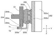
図4に示すハウジング204は、絶縁性の樹脂で成形される本体部204dを基体として、複数の接続部材204a、一以上の端子部204b、複数の壁部204cなどを有する。本体部204dは、長手方向Xが幅方向Yよりも長くなるように成形される。なお、長手方向Xと幅方向Yは、いずれも図2に示す外側面SOに沿う方向である。
The
複数の接続部材204aには、図3に破線で示すようにハウジング204の内部に配置される接続部材204aと、図4に示すようにハウジング204から外部に延びて幅方向Yに曲げられた接続部材204aとを含む。
The plurality of
一以上の端子部204bは、図3に示すように接続部材204aと接続されるとともに、図4に示すように幅方向Yに突出して設けられた部位である。なお、図4に示されるように端子部204bは接続部材204aよりも突出して成形してもよく、図示を省略するが接続部材204aよりも突出しないように成形してもよい。
The one or more
複数の壁部204cは、図4に示すように接続部材204aや端子部204bとは反対側の幅方向Y方向に突出しており、かつ、長手方向Xに向かい合うように設けられた部位である。長手方向Xにおける壁部204cの相互間には、二点鎖線で示す半導体モジュール203が配置される。図示しないが、図4における壁部204cと半導体モジュール203の上側には、図3に示すように冷却器202が配置される。
As shown in FIG. 4, the plurality of
半導体モジュール203に含まれる回路構成例について、図5〜図7を参照しながら説明する。半導体モジュール203は、図5に示す半導体モジュールM1、図6に示す半導体モジュールM2、図7に示す半導体モジュールM3などのうちで一以上を含む。なお半導体モジュール203には、半導体モジュールM1,M2,M3のほかに、後述する図8〜図12に示す内部リードフレーム203cや外部リードフレーム203dなども有する。半導体モジュールM1,M2,M3の各実現形態は任意であり、例えば基板上に半導体素子を配置して接続することで実現してもよく、半導体チップで実現してもよい。
An example of a circuit configuration included in the
図5に示す半導体モジュールM1は、IGBTのスイッチング素子Q1,Q2や、還流用のダイオードD1,D2などを有する。スイッチング素子Q1とダイオードD1は上アームに配置され、スイッチング素子Q2とダイオードD2は下アームに配置される。スイッチング素子Q1とスイッチング素子Q2は直列接続された素子ペアである。ダイオードD1はスイッチング素子Q1に並列接続され、ダイオードD2はスイッチング素子Q2に並列接続される。スイッチング素子Q1は、入力端子(例えばコレクタ端子など)が接続端子Pdに接続され、制御端子(例えばゲート端子など)が接続端子Pg1に接続される。スイッチング素子Q2は、出力端子(例えばエミッタ端子など)が接続端子Psに接続され、制御端子が接続端子Pg2に接続される。スイッチング素子Q1の出力端子とスイッチング素子Q2の入力端子とは接続点P1で接続されるとともに、接続端子Pm1に接続される。接続端子Pd,Pg1,Pg2,Ps,Pm1は、それぞれが内部リードフレーム203cで接続されたり、外部リードフレーム203dとして半導体モジュール203の外部に延びたりする。
The semiconductor module M1 shown in FIG. 5 includes IGBT switching elements Q1 and Q2, reflux diodes D1 and D2, and the like. The switching element Q1 and the diode D1 are disposed on the upper arm, and the switching element Q2 and the diode D2 are disposed on the lower arm. Switching element Q1 and switching element Q2 are a pair of elements connected in series. The diode D1 is connected in parallel to the switching element Q1, and the diode D2 is connected in parallel to the switching element Q2. The switching element Q1 has an input terminal (for example, a collector terminal) connected to the connection terminal Pd and a control terminal (for example, a gate terminal) connected to the connection terminal Pg1. The switching element Q2 has an output terminal (for example, an emitter terminal) connected to the connection terminal Ps and a control terminal connected to the connection terminal Pg2. The output terminal of the switching element Q1 and the input terminal of the switching element Q2 are connected at the connection point P1 and connected to the connection terminal Pm1. The connection terminals Pd, Pg1, Pg2, Ps, and Pm1 are each connected by an
図6に示す半導体モジュールM2は、MOSFETのスイッチング素子Q1,Q2などを有する。半導体モジュールM2は半導体モジュールM1と比べて、素子内部に寄生ダイオードを持つために外付けのダイオードD1,D2が無い点が相違する。スイッチング素子Q1の出力端子とスイッチング素子Q2の入力端子とは接続点P2で接続されるとともに、接続端子Pm1に接続される。接続端子Pd,Pg1,Pg2,Ps,Pm1は、それぞれが内部リードフレーム203cで接続されたり、外部リードフレーム203dとして半導体モジュール203の外部に延びたりする。図示を省略するが、半導体モジュールM1に適用したIGBTや、半導体モジュールM2に適用したMOSFETに代えて、JFET,MESFET,GTO,パワートランジスタなどを適用してもよい。
The semiconductor module M2 shown in FIG. 6 includes MOSFET switching elements Q1, Q2, and the like. The semiconductor module M2 is different from the semiconductor module M1 in that there are no external diodes D1 and D2 because the semiconductor module M2 has a parasitic diode inside the element. The output terminal of the switching element Q1 and the input terminal of the switching element Q2 are connected at the connection point P2 and connected to the connection terminal Pm1. The connection terminals Pd, Pg1, Pg2, Ps, and Pm1 are each connected by an
図7に示す半導体モジュールM3は、ダイオードD1,D2などを有する。半導体モジュールM3は半導体モジュールM1と比べて、スイッチング素子Q1,Q2が無い点が相違する。ダイオードD1とダイオードD2は直列接続された素子ペアである。ダイオードD1のカソード端子は接続端子Pkに接続される。ダイオードD2のアノード端子は接続端子Paに接続される。ダイオードD1のアノード端子とダイオードD2のカソード端子とは接続点P3で接続されるとともに、接続端子Pm2に接続される。接続端子Pk,Pa,Pm2は、それぞれが内部リードフレーム203cで接続されたり、外部リードフレーム203dとして半導体モジュール203の外部に延びたりする。
The semiconductor module M3 illustrated in FIG. 7 includes diodes D1, D2, and the like. The semiconductor module M3 is different from the semiconductor module M1 in that the switching elements Q1 and Q2 are not provided. The diode D1 and the diode D2 are element pairs connected in series. The cathode terminal of the diode D1 is connected to the connection terminal Pk. The anode terminal of the diode D2 is connected to the connection terminal Pa. The anode terminal of the diode D1 and the cathode terminal of the diode D2 are connected at the connection point P3 and also connected to the connection terminal Pm2. Each of the connection terminals Pk, Pa, Pm2 is connected by an
電力変換装置20の構成例について、図8〜図12を参照しながら説明する。図8〜図12では、半導体モジュール203に含まれるスイッチング素子Q1,Q2やダイオードD1,D2の図示を省略する。交差方向Zは、幅方向Yに交差する方向であり、本体部202bの長手方向に沿う方向である。
A configuration example of the
図8において、半導体モジュール203の所定面S2と、冷却器202の本体部202bとを面接触して接着するために、絶縁性の接着剤206を介在させる。接着剤206は、後述する図12に示す樹脂209よりも熱伝導性が高い材料の接着剤を用いるとよい。半導体モジュール203に内在される内部リードフレーム203cは、外部リードフレーム203dよりも板厚を大きくして、冷却部位203bに配置するとよい。冷却部位203bは、冷却器202と間接的に接する所定面S2を含む部位である。すなわち、内部リードフレーム203cは、冷却効率を高めるために、一部または全部がモールド樹脂203aから露出してもよい。半導体モジュール203から延びる外部リードフレーム203dは、幅方向Yにおいて冷却器202とは反対方向に曲げられる。
In FIG. 8, an insulating
図9において、ハウジング204から延びる接続部材204aにかかる先端部T1と、半導体モジュール203から延びる外部リードフレーム203dにかかる先端部T2とを揃える。接続部材204aは、外部リードフレーム203dと同様に、幅方向Yにおいて冷却器202とは反対方向に曲げられる。先端部T1,T2は、ハウジング204の対向面S1から外側の幅方向Y(例えば図9では左側)に突出して延びている。
In FIG. 9, the front end T1 applied to the
図10に示す接続部207は、先端部T1,T2を接続した部位である。電気的に接続が行えれば任意であり、本形態では溶接やハンダ付け等で接続を行う。先端部T1,T2がハウジング204の外側にあるので、接続作業を行い易い。そのため、接続部材204aと外部リードフレーム203dとは、ハウジング204の側面(例えば図10では下側面)に接近して延びていてもよい。
A connecting
図11において、対向面S1から接続部207まで外部リードフレーム203dと接続部材204aとを含めて囲うキャップ部208を設ける。キャップ部208を設けることによって、キャップ部208の内部空間SP1と、ハウジング204と冷却器202とで囲まれた空間SP2とが生じる。
In FIG. 11, a
キャップ部208は、断面がJ字状に成形される本体部位208cを基体とする。キャップ部208は、ハウジング204の対向面S1と接触するように設けられる。本体部位208cの一端部位208bは「先端部位」に相当し、嵌合部位208aが設けられる。嵌合部位208aは、ハウジング204の対向面S1に設けられる被嵌合部位204eと嵌合する。本形態では、嵌合部位208aを凸形状とし、被嵌合部位204eを凹形状とする。なお、キャップ部208は樹脂209で形成されてもよい。
The
またキャップ部208において、一端部位208bとは反対側の他端部位208dは、冷却器202の本体部202bに面接触するように設けられる。他端部位208dと本体部202bとの間は、後述する樹脂209の漏れを防止するため、図示しない接着剤で接着するとよい。当該接着剤は、接着剤206と同じ材料の接着剤でもよく、接着剤206とは異なる材料の接着剤でもよい。
In the
さらにキャップ部208は、対向面S1から幅方向Yに突出する高さが突出高H1である。突出高H1は、端子部204bが対向面S1から幅方向Yに突出する突出高H2よりも小さくなるように設定するとよい。この設定によれば、キャップ部208がハウジング204よりも突出しないので、電力変換装置20の体格を小さく抑えられる。
Further, the height of the
図12に示す電力変換装置20は、内部空間SP1と空間SP2とに樹脂209を充填した完成状態である。樹脂209は、ハウジング204の内部が被水したり、当該内部に粉塵が入ったりするのを防止する機能を担う。また樹脂209は、半導体モジュール203で発生した熱を冷却器202,ハウジング204およびキャップ部208を介して放熱する機能をも担う。絶縁性の樹脂209は、ハウジング204と冷却器202との間における開口側から充填する。樹脂209は、例えば充填後に固化する材料でもよく、充填後に液漏れしない程度の粘度を有する材料でもよい。
The
上述した実施の形態1によれば、以下に示す各作用効果を得ることができる。 According to the first embodiment described above, the following operational effects can be obtained.
(1)電力変換装置20は、図3〜図12に示すように、半導体モジュール203の所定面S2と間接的に面接触して冷却する冷却器202と、半導体モジュール203から延びて冷却器202とは反対方向に曲げられた複数の外部リードフレーム203dと、ハウジング204の内部に配置されるとともにハウジング204から延びて外部リードフレーム203dと同一方向に曲げられた複数の接続部材204aと、外部リードフレーム203dの先端部T2と接続部材204aの先端部T1とが接続された接続部207と、対向面S1から接続部207まで外部リードフレーム203dと接続部材204aとを含めて囲うキャップ部208と、ハウジング204と冷却器202とで囲まれた空間SP2とキャップ部208の内部空間SP1とに充填された絶縁性の樹脂209とを有する。この構成によれば、外部リードフレーム203dと接続部材204aの先端部T1,T2は、ともに所定面S2に対向するハウジング204の対向面S1から突出して延びている。ハウジング204に大きな開口部を確保する必要がなく、外部リードフレーム203dと接続部材204aが延びる方向の長さが抑えられる。よって、半導体モジュール203を含めた電力変換装置20全体の体格を従来よりも小型化できる。
(1) As shown in FIGS. 3 to 12, the
(2)半導体モジュール203は、図5〜図12に示すように、一以上の半導体素子がモールド樹脂203aによりモールドされる構成とした。この構成によれば、素子実装の小型化を図ることができる。
(2) The
(3)半導体モジュール203は、図8に示すように、所定面S2を含めて冷却器202によって冷却される冷却部位203bに配置され、外部リードフレーム203dよりも板厚が大きい内部リードフレーム203cを有する構成とした。この構成によれば、半導体素子(特に図5,図6に示すスイッチング素子Q1,Q2)で生じる熱を効率良く冷却器202に伝導することができる。
(3) As shown in FIG. 8, the
(4)半導体モジュール203は、図5〜図7に示すように、上アームに配置される半導体素子であるスイッチング素子Q1やダイオードD1と、下アームに配置される半導体素子であるスイッチング素子Q2やダイオードD2とが直列接続された素子ペアを一以上有する構成とした。この構成によれば、内部リードフレーム203cや外部リードフレーム203dの数を低減でき、実装面積の低減によって小型化を図ることができる。
(4) As shown in FIGS. 5 to 7, the
(6)図8〜図12に示すように、半導体モジュール203の所定面S2と冷却器202との間に介在され、樹脂209よりも熱伝導性が高い絶縁部材である接着剤206を有する構成とした。この構成によれば、半導体モジュール203で生じる熱を効率良く冷却器202に伝導して、半導体モジュール203を冷却することができる。
(6) As shown in FIGS. 8 to 12, a configuration having an adhesive 206 that is an insulating member that is interposed between the predetermined surface S <b> 2 of the
(7)キャップ部208の先端部位に相当する一端部位208bは、図11,図12に示すように、ハウジング204に設けられた被嵌合部位204eと嵌合する嵌合部位208aを有する構成とした。この構成によれば、ラビリンス構造とすることで充填された樹脂209の漏れをより確実に防止することができる。
(7) As shown in FIGS. 11 and 12, the one
(8)キャップ部208は、図4に示す壁部204cと同様に、図11,図12に示すようにハウジング204の一部として半導体モジュール203を囲う構成とした。この構成によれば、キャップ部208はハウジング204の一部として機能するので、小型化に寄与する。
(8) Similar to the
(9)回転電機10は、図1に示すように、回転子21と、回転子21に対向して設けられる固定子14と、回転子21を回転自在に支持するとともに固定子14を保持するフレーム12と、電力変換装置20とを有する構成とした。この構成によれば、電力変換装置20の体格が小さくなるので、回転電機10の体格も従来より小型化できる。
(9) As shown in FIG. 1, the rotating
(10)電力変換装置20のハウジング204は、図2に示すように、フレーム12の外側面SOに固定される構成とした。この構成によれば、固定子14で発生した熱が冷却器202に伝導するのを抑制することができる。
(10) The
〔実施の形態2〕
実施の形態2は図13〜図15を参照しながら説明する。なお図示および説明を簡単にするため、特に明示しない限り、実施の形態1で用いた要素と同一の要素には同一の符号を付して説明を省略する。よって、主に実施の形態1と相違する点を説明する。
[Embodiment 2]
The second embodiment will be described with reference to FIGS. For simplicity of illustration and description, unless otherwise specified, the same elements as those used in the first embodiment are denoted by the same reference numerals and description thereof is omitted. Therefore, differences from the first embodiment will be mainly described.
実施の形態2では、図13に示すように、対向する二面から複数の外部リードフレーム203dが延びる半導体モジュール203を適用する。例えば、図14の上側に延びる外部リードフレーム203dを高電圧用(例えば数百ボルト)とし、図14の下側に延びる外部リードフレーム203dを低電圧用(例えば数ボルト〜数十ボルト)として分けるとよい。同一面から延びる複数の外部リードフレーム203dにおける相互間で電位差が小さくなるので、ショート等による損傷を抑制することができる。
In the second embodiment, as shown in FIG. 13, a
図13の半導体モジュール203を用いて電力変換装置20を構成すると、図14のようになる。図14の上側に延びる外部リードフレーム203dは接続端子の機能を担う。
When the
図14の電力変換装置20は、下側にキャップ部208を備える。これに対して、さらに上側にもキャップ部208を備えた電力変換装置20を図15に示す。図15の電力変換装置20は、半導体モジュール203が全てハウジング204の内部に備えられるため、半導体モジュール203が露出しない。上側のキャップ部208は、内部空間SP1や空間SP2に樹脂209を充填するために、一以上の貫通孔208eを有する。貫通孔208eは、樹脂209を充填してもよく、図示しない蓋部材で塞いでもよい。
The
上述した実施の形態2によれば、実施の形態1と同様の作用効果を得ることができるとともに、次の作用効果を得ることができる。 According to the second embodiment described above, the same operational effects as those of the first embodiment can be obtained, and the following operational effects can be obtained.
(5)複数の外部リードフレーム203dは、図13〜図15に示すように、半導体モジュール203における対向する二面から延びる構成とした。図示を省略するが、対向することなく、異なる二面から延びる構成としてもよい。これらの構成によれば、電位差が大きな外部リードフレーム203dを二面に分けることで、腐食に対する信頼性を向上することができる。
(5) The plurality of external lead frames 203d are configured to extend from two opposing surfaces of the
〔他の実施の形態〕
以上では本発明を実施するための形態について実施の形態1,2に従って説明したが、本発明は当該形態に何ら限定されるものではない。言い換えれば、本発明の要旨を逸脱しない範囲内において、種々なる形態で実施することもできる。例えば、次に示す各形態を実現してもよい。
[Other Embodiments]
In the above, although the form for implementing this invention was demonstrated according to
上述した実施の形態1,2では、図11に示すように、嵌合部位208aを凸形状とし、被嵌合部位204eを凹形状として嵌合する構成とした。この形態に代えて、嵌合部位208aを凹形状とし、被嵌合部位204eを凸形状として嵌合する構成としてもよい。また、図16,図17に示すように嵌合部材210,211を用いて嵌合する構成としてもよい。図16では、嵌合部位208aと被嵌合部位204eの双方を凹形状とし、棒状または板状の嵌合部材210を用いて嵌合する。図17では、嵌合部位208aと被嵌合部位204eの双方を凸形状とし、筒状の嵌合部材211を用いて嵌合する。嵌合する部位の形状が相違するに過ぎないので、実施の形態1,2と同様の作用効果が得られる。
In the first and second embodiments described above, as shown in FIG. 11, the
上述した実施の形態1,2では、図2に示すように、三つの電力変換装置20A,20B,20Cを外側面SOに固定する構成とした。この形態に代えて、外側面SOに固定できる限りの範囲内において、三つを除く一以上の電力変換装置20を外側面SOに固定する構成としてもよい。電力変換装置20の数が相違するに過ぎないので、実施の形態1,2と同様の作用効果が得られる。
In the first and second embodiments described above, as shown in FIG. 2, the three
上述した実施の形態1,2では、図5〜図7に示すように、半導体モジュール203は半導体モジュールM1,M2,M3のうちで一以上を含む構成とした。この形態に代えて、半導体モジュールM1,M2,M3を一以上で任意に組み合わせて含めてもよい。例えば回転電機10が三相であれば、半導体モジュールM1を三つ組み合わせたり、半導体モジュールM2,M3をそれぞれ三つ組み合わせたりしてもよい。半導体モジュールM1,M2,M3には、コイル,コンデンサ,抵抗器などの電子部品を含めてもよい。半導体モジュール203に含める半導体モジュールの数や電子部品が相違するに過ぎないので、実施の形態1,2と同様の作用効果が得られる。
In the first and second embodiments described above, as shown in FIGS. 5 to 7, the
上述した実施の形態1,2では、図9〜図12,図14,図15に示すように、半導体モジュール203の所定面S2と冷却器202の本体部202bとの間に接着剤206を介在させて、間接的に面接触させる構成とした。この形態に代えて、所定面S2と本体部202bとを直接的に面接触させる構成としてもよい。この場合は、内部リードフレーム203cが半導体モジュール203から露出しないように構成するとよい。間接的か直接的かの相違に過ぎないので、実施の形態1,2と同様の作用効果が得られる。
In the first and second embodiments described above, an adhesive 206 is interposed between the predetermined surface S2 of the
上述した実施の形態1,2では、図3に示すように、複数のフィン部202aを有する空冷式の冷却器202を適用する構成とした。この形態に代えて、水冷式の冷却器を適用する構成としてもよい。水冷式の冷却器は、冷却流体を導入する導入口、冷却流体が流れる冷却水路、冷却流体を排出する排出口などを有する。冷却流体は、例えば冷却水や冷却油などが該当し、外部に設けられるポンプとの間で循環する。冷却流体によって強制的に半導体モジュール203を冷却することができる。その他については、実施の形態1,2と同様の作用効果が得られる。
In the first and second embodiments described above, an air-cooled
上述した実施の形態1,2では、図1に示すように、インナーロータ型の回転電機10に適用した。この形態に代えて、アウターロータ型の回転電機10に適用してもよい。また、対向する回転子コア21a,21cに代えて、回転子コア21a,21cを一体化した回転子コアを適用してもよい。回転子21に回転子巻線21bを備える構成に代えて、回転子巻線21bを備えない構成としてもよい。回転子巻線21bに通電する必要が無くなるので、ブラシホルダ16やスリップリング18などが不要になる。フロントフレーム12Fとリアフレーム12Rとに代えて、フロントフレーム12Fとリアフレーム12Rとを一体化させた一体フレームでフレーム12を構成してもよい。フレーム12には、上述した水冷式の冷却器と同様に、さらに導入口,冷却水路,排出口を設けてもよい。冷却流体による強制冷却と、冷却風による冷却と合わせて、回転電機10をさらに冷却することができる。いずれの構成にせよ、実施の形態1,2と同様の作用効果が得られる。
The first and second embodiments described above are applied to the inner rotor type rotating
上述した実施の形態1,2では、図1に示すように、固定子コア14bと回転子コア21a,21cを積層鋼板で構成し、さらに回転子コア21a,21cは爪状磁極を備える構成とした。この形態に代えて、固定子コア14bおよび回転子コア21a,21cの少なくとも一方を単体の磁性体で構成してもよく、起磁力源となる一以上の永久磁石を備える構成としてもよく、磁性材と永久磁石を組み合わせる構成としてもよい。永久磁石を備える構成では、磁極を流れる磁束によるリラクタンストルクに加えて、永久磁石によるマグネットトルクが加わるので、さらにトルク性能を向上させることができる。爪状磁極を永久磁石で構成すれば、回転子巻線21bの巻数を低減したり、無くしたりすることが可能になる。回転子巻線21bが小さくなる(あるいは無くなる)分だけ、回転電機10の体格を小さく抑制できる。その他については、起磁力源の相違に過ぎないので、実施の形態1,2と同様の作用効果が得られる。
In the first and second embodiments described above, as shown in FIG. 1, the
上述した実施の形態1,2では、図1に示すように、回転子21と冷却ファン13を別体に成形して固定する構成とした。この形態に代えて、回転子21(具体的には回転子コア21a,21c)と冷却ファン13を一体成形する構成としてもよい。別体成形か一体成形かの相違に過ぎないので、実施の形態1,2と同様の作用効果が得られる。
In the first and second embodiments described above, the
10 回転電機
20,20A,20B,20C 電力変換装置
202 冷却器
203 半導体モジュール
203d 外部リードフレーム
204 ハウジング
204a 接続部材
207 接続部
208 キャップ部
209 樹脂
DESCRIPTION OF
Claims (10)
前記半導体モジュールの所定面(S2)と直接的または間接的に面接触して冷却する冷却器(202)と、
前記半導体モジュールから延びて前記冷却器とは反対方向に曲げられた複数の外部リードフレーム(203d)と、
前記ハウジングの内部に配置されるとともに、前記ハウジングから延びて前記外部リードフレームと同一方向に曲げられた複数の接続部材(204a)と、
前記外部リードフレームの先端部(T2)と前記接続部材の先端部(T1)とは、ともに前記所定面に対向する前記ハウジングの対向面(S1)から突出して延びており、前記先端部どうしが電気的に接続された接続部(207)と、
前記対向面から前記接続部まで、前記外部リードフレームと前記接続部材とを含めて囲うキャップ部(208)と、
前記ハウジングと前記冷却器とで囲まれた空間(SP2)と、前記キャップ部の内部空間(SP1)とに充填された絶縁性の樹脂(209)とを有する電力変換装置(20,20A,20B,20C)。 A stator winding (14a) of the rotating electrical machine (10) and an external DC power source (E) are provided by a semiconductor module (203) including one or more semiconductor elements (Q1, Q2, D1, D2) inside the housing (204). In the power conversion device that converts power to
A cooler (202) that cools in direct or indirect surface contact with a predetermined surface (S2) of the semiconductor module;
A plurality of external lead frames (203d) extending from the semiconductor module and bent in a direction opposite to the cooler;
A plurality of connecting members (204a) disposed inside the housing and extending from the housing and bent in the same direction as the external lead frame;
Both the distal end portion (T2) of the external lead frame and the distal end portion (T1) of the connection member protrude from the facing surface (S1) of the housing facing the predetermined surface, and the distal end portions are connected to each other. An electrically connected connection (207);
A cap portion (208) enclosing and including the external lead frame and the connection member from the facing surface to the connection portion;
A power converter (20, 20A, 20B) having a space (SP2) surrounded by the housing and the cooler and an insulating resin (209) filled in the internal space (SP1) of the cap portion. , 20C).
請求項1から8のいずれか一項に記載の電力変換装置を一以上有する回転電機。 A rotor (21); a stator (14) provided opposite to the rotor; and a frame (12, 12F, 12R) that rotatably supports the rotor and holds the stator. In the rotating electrical machine (10),
The rotary electric machine which has one or more the power converter devices as described in any one of Claim 1 to 8.
Priority Applications (5)
| Application Number | Priority Date | Filing Date | Title |
|---|---|---|---|
| JP2015247935A JP6485705B2 (en) | 2015-12-18 | 2015-12-18 | Power converter and rotating electric machine |
| FR1662610A FR3045977B1 (en) | 2015-12-18 | 2016-12-16 | ENERGY CONVERTER AND ROTARY ELECTRIC MACHINE |
| CN201611168801.4A CN106898592B (en) | 2015-12-18 | 2016-12-16 | Power converter and rotating electrical machine |
| DE102016124627.1A DE102016124627B4 (en) | 2015-12-18 | 2016-12-16 | Power conversion device and rotating electric machine |
| US15/383,985 US10396636B2 (en) | 2015-12-18 | 2016-12-19 | Power converter and rotary electric machine |
Applications Claiming Priority (1)
| Application Number | Priority Date | Filing Date | Title |
|---|---|---|---|
| JP2015247935A JP6485705B2 (en) | 2015-12-18 | 2015-12-18 | Power converter and rotating electric machine |
Publications (2)
| Publication Number | Publication Date |
|---|---|
| JP2017112808A JP2017112808A (en) | 2017-06-22 |
| JP6485705B2 true JP6485705B2 (en) | 2019-03-20 |
Family
ID=58994707
Family Applications (1)
| Application Number | Title | Priority Date | Filing Date |
|---|---|---|---|
| JP2015247935A Active JP6485705B2 (en) | 2015-12-18 | 2015-12-18 | Power converter and rotating electric machine |
Country Status (5)
| Country | Link |
|---|---|
| US (1) | US10396636B2 (en) |
| JP (1) | JP6485705B2 (en) |
| CN (1) | CN106898592B (en) |
| DE (1) | DE102016124627B4 (en) |
| FR (1) | FR3045977B1 (en) |
Families Citing this family (4)
| Publication number | Priority date | Publication date | Assignee | Title |
|---|---|---|---|---|
| CN108233657B (en) * | 2016-12-22 | 2020-06-16 | 博格华纳公司 | Alternator with external ignition protection system |
| US10707716B2 (en) | 2017-11-20 | 2020-07-07 | Borgwarner Inc. | Stator core and stator slot closer |
| JP7547702B2 (en) * | 2018-09-28 | 2024-09-10 | ニデックパワートレインシステムズ株式会社 | Electric pump device |
| WO2020129112A1 (en) * | 2018-12-17 | 2020-06-25 | 三菱電機株式会社 | Rotating electric machine |
Family Cites Families (15)
| Publication number | Priority date | Publication date | Assignee | Title |
|---|---|---|---|---|
| JP2002058172A (en) | 2000-08-11 | 2002-02-22 | Denso Corp | Voltage controller of vehicle alternator |
| US7262973B2 (en) * | 2003-08-29 | 2007-08-28 | Matsushita Electric Industrial Co., Ltd. | Power conversion module device and power unit using the same |
| JP5369798B2 (en) * | 2009-03-18 | 2013-12-18 | 富士電機株式会社 | Semiconductor device and manufacturing method thereof |
| JP5446937B2 (en) | 2009-06-24 | 2014-03-19 | 株式会社デンソー | Motor with built-in electronic circuit |
| JP5532984B2 (en) | 2010-02-04 | 2014-06-25 | 株式会社デンソー | Rotating electric machine for vehicles |
| US8513784B2 (en) * | 2010-03-18 | 2013-08-20 | Alpha & Omega Semiconductor Incorporated | Multi-layer lead frame package and method of fabrication |
| JP5300784B2 (en) * | 2010-05-21 | 2013-09-25 | 三菱電機株式会社 | Semiconductor module and rotating electric machine equipped with semiconductor module |
| JP5721852B2 (en) | 2011-10-25 | 2015-05-20 | 三菱電機株式会社 | Rotating electric machine |
| JP5143317B1 (en) | 2012-04-06 | 2013-02-13 | 三菱電機株式会社 | Air conditioner indoor unit |
| JP5488638B2 (en) * | 2012-04-11 | 2014-05-14 | 株式会社デンソー | Power converter |
| EP2840687B1 (en) | 2012-04-16 | 2019-06-26 | Mitsubishi Electric Corporation | Dynamo-electric machine |
| JP5602786B2 (en) * | 2012-05-07 | 2014-10-08 | 三菱電機株式会社 | Rotating electric machine |
| EP2738809A3 (en) * | 2012-11-30 | 2017-05-10 | Enpirion, Inc. | Semiconductor device including gate drivers around a periphery thereof |
| JP5752218B2 (en) | 2013-12-09 | 2015-07-22 | 三菱電機株式会社 | Rotating electric machine with power converter |
| DE112015004606T5 (en) * | 2014-10-08 | 2017-07-06 | Remy Technologies, Llc | Base surface for MOSFET module |
-
2015
- 2015-12-18 JP JP2015247935A patent/JP6485705B2/en active Active
-
2016
- 2016-12-16 FR FR1662610A patent/FR3045977B1/en active Active
- 2016-12-16 DE DE102016124627.1A patent/DE102016124627B4/en active Active
- 2016-12-16 CN CN201611168801.4A patent/CN106898592B/en active Active
- 2016-12-19 US US15/383,985 patent/US10396636B2/en active Active
Also Published As
| Publication number | Publication date |
|---|---|
| FR3045977A1 (en) | 2017-06-23 |
| DE102016124627B4 (en) | 2022-10-06 |
| DE102016124627A1 (en) | 2017-06-22 |
| US20170179796A1 (en) | 2017-06-22 |
| FR3045977B1 (en) | 2019-04-05 |
| CN106898592B (en) | 2021-01-29 |
| CN106898592A (en) | 2017-06-27 |
| US10396636B2 (en) | 2019-08-27 |
| JP2017112808A (en) | 2017-06-22 |
Similar Documents
| Publication | Publication Date | Title |
|---|---|---|
| JP4147987B2 (en) | Multi-phase AC rotating electric machine | |
| US8970076B2 (en) | Controller-integrated rotating electrical machine | |
| JP5752218B2 (en) | Rotating electric machine with power converter | |
| US9812929B2 (en) | Electric rotating machine | |
| JP6621491B2 (en) | Rotating electric machine | |
| JP2012147564A (en) | Rotary electric machine unit | |
| JP2005532025A (en) | Control power module for integrated alternator starter | |
| JP6371001B2 (en) | Power converter | |
| JP6485705B2 (en) | Power converter and rotating electric machine | |
| US10263495B2 (en) | Rotary electric machine | |
| JP5787226B2 (en) | Rotating electric machine for vehicles | |
| CN113141088B (en) | Rotary electric machine | |
| JP4089917B2 (en) | Motor generator for vehicles | |
| US20200100393A1 (en) | Motor, printed circuit board, and engine cooling fan module including the motor | |
| US11581786B2 (en) | Rotary electric machine | |
| JP4470879B2 (en) | Power generation control device for vehicle generator | |
| JP2005224044A (en) | Power generation dynamo-electric apparatus for vehicle | |
| JP3972855B2 (en) | Inverter module | |
| JP7250087B1 (en) | Rotating electric machine and its manufacturing method | |
| JP7166408B1 (en) | Rotating electric machine | |
| JP7113945B1 (en) | Rotating electric machine | |
| KR102063994B1 (en) | Alternator for Vehicle | |
| JP2006158200A (en) | Ac generator for vehicle | |
| JP2015171211A (en) | Electric fluid pump for internal combustion engine | |
| JP2005245150A (en) | Rotary electric machine for vehicle |
Legal Events
| Date | Code | Title | Description |
|---|---|---|---|
| A621 | Written request for application examination |
Free format text: JAPANESE INTERMEDIATE CODE: A621 Effective date: 20180405 |
|
| TRDD | Decision of grant or rejection written | ||
| A01 | Written decision to grant a patent or to grant a registration (utility model) |
Free format text: JAPANESE INTERMEDIATE CODE: A01 Effective date: 20190124 |
|
| A977 | Report on retrieval |
Free format text: JAPANESE INTERMEDIATE CODE: A971007 Effective date: 20190123 |
|
| A61 | First payment of annual fees (during grant procedure) |
Free format text: JAPANESE INTERMEDIATE CODE: A61 Effective date: 20190206 |
|
| R151 | Written notification of patent or utility model registration |
Ref document number: 6485705 Country of ref document: JP Free format text: JAPANESE INTERMEDIATE CODE: R151 |
|
| R250 | Receipt of annual fees |
Free format text: JAPANESE INTERMEDIATE CODE: R250 |
|
| R250 | Receipt of annual fees |
Free format text: JAPANESE INTERMEDIATE CODE: R250 |
|
| R250 | Receipt of annual fees |
Free format text: JAPANESE INTERMEDIATE CODE: R250 |