JP5396215B2 - Semiconductor light emitting device manufacturing method, semiconductor light emitting device, and liquid crystal display device - Google Patents
Semiconductor light emitting device manufacturing method, semiconductor light emitting device, and liquid crystal display device Download PDFInfo
- Publication number
- JP5396215B2 JP5396215B2 JP2009219476A JP2009219476A JP5396215B2 JP 5396215 B2 JP5396215 B2 JP 5396215B2 JP 2009219476 A JP2009219476 A JP 2009219476A JP 2009219476 A JP2009219476 A JP 2009219476A JP 5396215 B2 JP5396215 B2 JP 5396215B2
- Authority
- JP
- Japan
- Prior art keywords
- light
- light emitting
- emitting element
- emitting device
- substrate
- Prior art date
- Legal status (The legal status is an assumption and is not a legal conclusion. Google has not performed a legal analysis and makes no representation as to the accuracy of the status listed.)
- Active
Links
- 239000004065 semiconductor Substances 0.000 title claims description 85
- 238000004519 manufacturing process Methods 0.000 title claims description 30
- 239000004973 liquid crystal related substance Substances 0.000 title claims description 17
- 229920005989 resin Polymers 0.000 claims description 73
- 239000011347 resin Substances 0.000 claims description 73
- 239000003566 sealing material Substances 0.000 claims description 50
- 239000000758 substrate Substances 0.000 claims description 47
- 125000006850 spacer group Chemical group 0.000 claims description 36
- 238000000034 method Methods 0.000 claims description 31
- 238000001579 optical reflectometry Methods 0.000 claims description 11
- 239000002245 particle Substances 0.000 claims description 9
- GWEVSGVZZGPLCZ-UHFFFAOYSA-N Titan oxide Chemical compound O=[Ti]=O GWEVSGVZZGPLCZ-UHFFFAOYSA-N 0.000 claims description 5
- OGIDPMRJRNCKJF-UHFFFAOYSA-N titanium oxide Inorganic materials [Ti]=O OGIDPMRJRNCKJF-UHFFFAOYSA-N 0.000 claims description 5
- 239000011248 coating agent Substances 0.000 claims description 2
- 238000000576 coating method Methods 0.000 claims description 2
- 239000000565 sealant Substances 0.000 claims 1
- 238000007789 sealing Methods 0.000 claims 1
- 239000000463 material Substances 0.000 description 12
- ORQBXQOJMQIAOY-UHFFFAOYSA-N nobelium Chemical compound [No] ORQBXQOJMQIAOY-UHFFFAOYSA-N 0.000 description 11
- 230000003287 optical effect Effects 0.000 description 7
- 229920002050 silicone resin Polymers 0.000 description 7
- 238000001179 sorption measurement Methods 0.000 description 6
- 238000010438 heat treatment Methods 0.000 description 5
- OAICVXFJPJFONN-UHFFFAOYSA-N Phosphorus Chemical compound [P] OAICVXFJPJFONN-UHFFFAOYSA-N 0.000 description 4
- 230000001681 protective effect Effects 0.000 description 4
- 239000004593 Epoxy Substances 0.000 description 3
- 230000000052 comparative effect Effects 0.000 description 3
- 239000011521 glass Substances 0.000 description 3
- 230000009974 thixotropic effect Effects 0.000 description 3
- RYGMFSIKBFXOCR-UHFFFAOYSA-N Copper Chemical compound [Cu] RYGMFSIKBFXOCR-UHFFFAOYSA-N 0.000 description 2
- 238000000149 argon plasma sintering Methods 0.000 description 2
- 239000011889 copper foil Substances 0.000 description 2
- 239000012780 transparent material Substances 0.000 description 2
- 238000010521 absorption reaction Methods 0.000 description 1
- 230000002238 attenuated effect Effects 0.000 description 1
- 238000001816 cooling Methods 0.000 description 1
- 239000008393 encapsulating agent Substances 0.000 description 1
- 229910052737 gold Inorganic materials 0.000 description 1
- 238000002347 injection Methods 0.000 description 1
- 239000007924 injection Substances 0.000 description 1
- 229910052751 metal Inorganic materials 0.000 description 1
- 239000002184 metal Substances 0.000 description 1
- 229910052709 silver Inorganic materials 0.000 description 1
- 229910000679 solder Inorganic materials 0.000 description 1
- 238000004544 sputter deposition Methods 0.000 description 1
- 230000008961 swelling Effects 0.000 description 1
Images


Classifications
-
- H01L33/46—
-
- H—ELECTRICITY
- H01—ELECTRIC ELEMENTS
- H01L—SEMICONDUCTOR DEVICES NOT COVERED BY CLASS H10
- H01L24/00—Arrangements for connecting or disconnecting semiconductor or solid-state bodies; Methods or apparatus related thereto
- H01L24/93—Batch processes
- H01L24/95—Batch processes at chip-level, i.e. with connecting carried out on a plurality of singulated devices, i.e. on diced chips
- H01L24/97—Batch processes at chip-level, i.e. with connecting carried out on a plurality of singulated devices, i.e. on diced chips the devices being connected to a common substrate, e.g. interposer, said common substrate being separable into individual assemblies after connecting
-
- H—ELECTRICITY
- H01—ELECTRIC ELEMENTS
- H01L—SEMICONDUCTOR DEVICES NOT COVERED BY CLASS H10
- H01L2224/00—Indexing scheme for arrangements for connecting or disconnecting semiconductor or solid-state bodies and methods related thereto as covered by H01L24/00
- H01L2224/01—Means for bonding being attached to, or being formed on, the surface to be connected, e.g. chip-to-package, die-attach, "first-level" interconnects; Manufacturing methods related thereto
- H01L2224/42—Wire connectors; Manufacturing methods related thereto
- H01L2224/47—Structure, shape, material or disposition of the wire connectors after the connecting process
- H01L2224/48—Structure, shape, material or disposition of the wire connectors after the connecting process of an individual wire connector
- H01L2224/4805—Shape
- H01L2224/4809—Loop shape
- H01L2224/48091—Arched
-
- H—ELECTRICITY
- H01—ELECTRIC ELEMENTS
- H01L—SEMICONDUCTOR DEVICES NOT COVERED BY CLASS H10
- H01L2224/00—Indexing scheme for arrangements for connecting or disconnecting semiconductor or solid-state bodies and methods related thereto as covered by H01L24/00
- H01L2224/01—Means for bonding being attached to, or being formed on, the surface to be connected, e.g. chip-to-package, die-attach, "first-level" interconnects; Manufacturing methods related thereto
- H01L2224/42—Wire connectors; Manufacturing methods related thereto
- H01L2224/47—Structure, shape, material or disposition of the wire connectors after the connecting process
- H01L2224/48—Structure, shape, material or disposition of the wire connectors after the connecting process of an individual wire connector
- H01L2224/481—Disposition
- H01L2224/48151—Connecting between a semiconductor or solid-state body and an item not being a semiconductor or solid-state body, e.g. chip-to-substrate, chip-to-passive
- H01L2224/48221—Connecting between a semiconductor or solid-state body and an item not being a semiconductor or solid-state body, e.g. chip-to-substrate, chip-to-passive the body and the item being stacked
- H01L2224/48245—Connecting between a semiconductor or solid-state body and an item not being a semiconductor or solid-state body, e.g. chip-to-substrate, chip-to-passive the body and the item being stacked the item being metallic
- H01L2224/48247—Connecting between a semiconductor or solid-state body and an item not being a semiconductor or solid-state body, e.g. chip-to-substrate, chip-to-passive the body and the item being stacked the item being metallic connecting the wire to a bond pad of the item
-
- H—ELECTRICITY
- H01—ELECTRIC ELEMENTS
- H01L—SEMICONDUCTOR DEVICES NOT COVERED BY CLASS H10
- H01L2224/00—Indexing scheme for arrangements for connecting or disconnecting semiconductor or solid-state bodies and methods related thereto as covered by H01L24/00
- H01L2224/80—Methods for connecting semiconductor or other solid state bodies using means for bonding being attached to, or being formed on, the surface to be connected
- H01L2224/85—Methods for connecting semiconductor or other solid state bodies using means for bonding being attached to, or being formed on, the surface to be connected using a wire connector
- H01L2224/85909—Post-treatment of the connector or wire bonding area
- H01L2224/8592—Applying permanent coating, e.g. protective coating
-
- H—ELECTRICITY
- H01—ELECTRIC ELEMENTS
- H01L—SEMICONDUCTOR DEVICES NOT COVERED BY CLASS H10
- H01L2924/00—Indexing scheme for arrangements or methods for connecting or disconnecting semiconductor or solid-state bodies as covered by H01L24/00
- H01L2924/10—Details of semiconductor or other solid state devices to be connected
- H01L2924/11—Device type
- H01L2924/12—Passive devices, e.g. 2 terminal devices
- H01L2924/1204—Optical Diode
- H01L2924/12041—LED
-
- H01L33/58—
-
- H01L33/60—
Landscapes
- Engineering & Computer Science (AREA)
- Computer Hardware Design (AREA)
- Microelectronics & Electronic Packaging (AREA)
- Power Engineering (AREA)
- Led Device Packages (AREA)
- Liquid Crystal (AREA)
Description
本発明は、発光素子(LED)を搭載した半導体発光装置に関し、特に、液晶表示装置のエッジライト型バックライトの用途に適した半導体発光装置に関する。 The present invention relates to a semiconductor light emitting device equipped with a light emitting element (LED), and more particularly to a semiconductor light emitting device suitable for use in an edge light type backlight of a liquid crystal display device.
液晶表示装置には、液晶パネルの背面に発光素子を配置する直下型バックライトと、液晶パネルの背面に導光板を配置し、導光板の端部に発光素子を線状に配列した光源を配置するエッジライト型バックライトが知られている。 The liquid crystal display device has a direct-type backlight in which light emitting elements are arranged on the back of the liquid crystal panel, and a light source in which light guide plates are arranged on the back of the liquid crystal panel and light emitting elements are arranged linearly at the ends of the light guide plate. Edge light type backlights are known.
液晶表示装置の薄型化に伴い、導光板および光源を薄型化することが望まれている。例えば、特許文献1には、発光素子(LEDチップ)の上面を導光板に向けた構造で、薄型化が可能で樹脂の使用量を低減した光源モジュールの構成が開示されている。特許文献2には、発光素子の側面を導光板に向け、導光板に向いた面以外の側面三方を反射面で囲み、下面および上面をそれぞれ基板で挟んだ構造が開示されている。反射面で囲まれた発光素子の周囲は透光性樹脂により充填されている。
As the liquid crystal display device becomes thinner, it is desired to reduce the thickness of the light guide plate and the light source. For example,
特許文献2に記載のように、発光素子の側面を導光板側に向けた、いわゆるサイドビュー型の発光装置では、図12(a),(b)に示したように、発光素子102は、基板100、側面部材104、上面基板105で囲まれ、側面に光放出口103を備えたキャビティ内に配置される。発光素子102の光放出口103側とは逆側の側面部材104(背面側の反射面101)に向かって発光素子102から出射された光は、反射面101で反射されて光放出口103に向かうため、光放出口103から出射されるまでの光路が長い。このため、光は、発光素子102の周囲空間を充填する封止材により減衰するという問題がある。
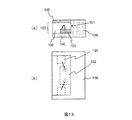
As described in
これを改善するためには、図13(a)、(b)のように、背面側の反射面101に接触するように発光素子102を配置することが考えられる。しかしながら、図14(a)に示すように一般的には製造工程において発光素子102をキャビティ内に配置する際に、発光素子102を吸着冶具107の先端に吸着保持して移動させ、位置決めして配置するため、側面部材104に接触するように配置することは容易ではない。例えば図14(b)のように、吸着冶具107の径が発光素子102より大きいと、吸着冶具107が側面部材104にぶつかるため、発光素子102を側面部材104に接触させて配置することはできない。また、図14(c)のように吸着冶具107の径が発光素子102より小さくても、吸着冶具107の基板100主平面方向への移動精度が低いと、発光素子102が側面部材104の上面に衝突し、発光素子102を側面部材104の側面に接触して配置することはできない。
In order to improve this, it is conceivable to arrange the
本発明の目的は、発光効率の高い側面発光型の半導体発光装置の製造方法を提供することにある。 An object of the present invention is to provide a method for manufacturing a side-emitting semiconductor light-emitting device with high luminous efficiency.
上記目的を達成するために、本発明の第1の態様によれば、以下のような半導体発光装置の製造方法が提供される。すなわち、所定の電極パターンを有する基板上に、発光素子を配置する工程と、発光素子と所定の空間を空けて基板上に側壁部材を配置する工程と、発光素子と電極パターンとを電気的に接続する工程と、発光素子の側面の少なくとも一部と、側壁部材との間の空間に光反射性樹脂を充填する工程と、発光素子の周囲に発光素子からの光を透過する封止材を充填する工程と、少なくとも封止材の上面に光反射性を有する天井部を配置する工程、とを有する半導体発光装置の製造方法である。 In order to achieve the above object, according to the first aspect of the present invention, the following method for manufacturing a semiconductor light emitting device is provided. That is, a step of disposing a light emitting element on a substrate having a predetermined electrode pattern, a step of disposing a side wall member on the substrate with a predetermined space from the light emitting element, and electrically connecting the light emitting element and the electrode pattern. A step of connecting, a step of filling a light reflective resin in a space between at least a part of the side surface of the light emitting element and the side wall member, and a sealing material that transmits light from the light emitting element around the light emitting element A method of manufacturing a semiconductor light emitting device, comprising: a filling step; and a step of disposing at least an upper surface of a sealing material having light reflectivity.
例えば、上述の側壁部材は、光放出口となる方向を前面としたときの発光素子の両脇側面と背面を囲み、光反射性樹脂は、背面側の側壁部材と発光素子の背面との間に充填されるように構成する。 For example, the above-mentioned side wall member surrounds both side surfaces and the back surface of the light emitting element when the direction to be the light emission port is the front surface, and the light reflective resin is between the side wall member on the back side and the back surface of the light emitting element. It is comprised so that it may be filled.
例えば、上述の光反射性樹脂を充填する工程では、未硬化の光反射性樹脂を充填後、未硬化の封止材樹脂を充填し、光反射性樹脂と封止材樹脂を同時に硬化させることが可能である。 For example, in the above-described step of filling the light reflecting resin, after filling the uncured light reflecting resin, filling the uncured sealing material resin and simultaneously curing the light reflecting resin and the sealing material resin. Is possible.
例えば、上述の接続する工程は、ワイヤを発光素子の背面方向の電極パターンと接続し、光反射性樹脂を充填する工程は、発光素子の背面方向のワイヤの形状を維持したまま埋め込むように、発光素子の背面とスペーサとの間の空間に光反射性樹脂を充填することが可能である。 For example, the connecting step described above connects the wire to the electrode pattern in the back direction of the light emitting element, and the step of filling the light reflecting resin embeds the wire while maintaining the shape of the wire in the back direction of the light emitting element. It is possible to fill the space between the back surface of the light emitting element and the spacer with a light reflective resin.
例えば、上述の光反射性樹脂を充填する工程は、前記発光素子の前記背面と前記スペーサとの間の空間で光反射性樹脂が発光素子上面よりも高い位置において上向きのふくらみを持つ形状に盛り上がるようにチクソ性、もしくは粘度を調整した樹脂を用いることができる。 For example, in the step of filling the light-reflecting resin, the light-reflecting resin rises in a shape having an upward bulge at a position higher than the upper surface of the light emitting element in the space between the back surface of the light emitting element and the spacer. Thus, thixotropic or viscosity-adjusted resins can be used.
また、本発明の第2の態様によれば、以下のような半導体発光装置の製造方法が提供される。すなわち、所定の電極パターンを有する基板上に、発光素子を配置し、発光素子と電極パターンとを電気的に接続する工程と、発光素子の側面の少なくとも一部に接するように基板上の空間を光反射性樹脂で充填する工程と、発光素子の周囲に発光素子からの光を透過する封止材を充填する工程と、少なくとも封止材の上面に光反射膜を形成する工程、とを有する半導体発光装置の製造方法である。 Moreover, according to the 2nd aspect of this invention, the manufacturing method of the following semiconductor light-emitting devices is provided. That is, a step of arranging a light emitting element on a substrate having a predetermined electrode pattern, electrically connecting the light emitting element and the electrode pattern, and a space on the substrate so as to be in contact with at least a part of the side surface of the light emitting element. A step of filling with a light-reflective resin, a step of filling a sealing material that transmits light from the light-emitting element around the light-emitting element, and a step of forming a light-reflecting film on at least the upper surface of the sealing material. A method for manufacturing a semiconductor light emitting device.
また、本発明の第3の態様によれば、以下のような半導体発光装置が提供される。すなわち、基板と、基板上に搭載された少なくとも一つの発光素子と、発光素子の側面のうち前面に開口を有し、両脇面と背面を所定の空間をあけて囲む側壁部材とを有する半導体発光装置である。発光素子の背面と側壁部材との間の空間には、発光素子の背面側の側面を覆うように、光反射性部材が充填され、反射性部材が配置されていない発光素子の側面と側壁部材との間は、前記発光素子からの光を透過する封止材で封止され、少なくとも封止材の上面は、光反射性を有する天井部で覆われている。 Moreover, according to the 3rd aspect of this invention, the following semiconductor light-emitting devices are provided. That is, a semiconductor having a substrate, at least one light-emitting element mounted on the substrate, and a side wall member that has an opening in the front surface among the side surfaces of the light-emitting element and surrounds both side surfaces and the back surface with a predetermined space therebetween It is a light emitting device. The space between the back surface of the light emitting element and the side wall member is filled with the light reflecting member so as to cover the side surface on the back surface side of the light emitting element, and the side surface and side wall member of the light emitting element on which the reflective member is not disposed Are sealed with a sealing material that transmits light from the light emitting element, and at least the upper surface of the sealing material is covered with a ceiling portion having light reflectivity.
例えば、上述の発光素子の背面と側壁部材との間の空間には、基板上に備えられた電極と発光素子とを接続する湾曲したワイヤが配置され、光反射性部材は、湾曲したワイヤを埋め込んでいる構成にすることができる。 For example, a curved wire that connects the electrode provided on the substrate and the light emitting element is disposed in the space between the back surface of the light emitting element and the side wall member, and the light reflective member includes a curved wire. It can be configured to be embedded.
例えば、上述の発光素子の背面と前記側壁部材との間の空間には、電子回路素子が配置され、光反射性部材は、電子回路素子を埋め込んでいる構成にすることも可能である。 For example, an electronic circuit element may be arranged in a space between the back surface of the light emitting element and the side wall member, and the light reflective member may be embedded in the electronic circuit element.
本発明の第4の態様によれば、以下のような半導体発光装置が提供される。すなわち、基板と、基板上に搭載された発光素子と、発光素子の側面の少なくとも一部を覆い周囲空間の一部を充填する光反射性部材と、発光素子の光反射性部材で覆っているところ以外を覆う発光素子の光を透過する封止材と、少なくとも封止材の上面を覆う光反射性を有する天井部とを有する半導体発光装置である。光反射性部材は、天井部に接するように空間を充填している。 According to the fourth aspect of the present invention, the following semiconductor light emitting device is provided. That is, the substrate, the light-emitting element mounted on the substrate, the light-reflecting member that covers at least part of the side surface of the light-emitting element and fills part of the surrounding space, and the light-reflecting member of the light-emitting element are covered. A semiconductor light-emitting device having a sealing material that transmits light from a light-emitting element that covers other than the above, and a light-reflective ceiling that covers at least the upper surface of the sealing material. The light reflective member fills the space so as to be in contact with the ceiling.
本発明の第5の態様によれば、以下のような液晶表示装置が提供される。すなわち、液晶パネルと、液晶パネルの背面に配置された導光板と、導光板の端面に配置された半導体発光装置とを有する液晶表示装置である。半導体発光装置は、基板と、基板上に搭載された少なくとも一つの発光素子と、発光素子の側面のうち前面に開口を有し、両脇面と背面を所定の空間をあけて囲む側壁部材とを有する。発光素子の背面と側壁部材との間の空間には、少なくとも発光素子の背面側の側面を覆うように、光反射性部材が充填されている。反射性部材が配置されていない発光素子の側面と側壁部材との間は、発光素子からの光を透過する封止材で封止される。少なくとも封止材の上面は、光反射性を有する天井部で覆われている。 According to the fifth aspect of the present invention, the following liquid crystal display device is provided. That is, the liquid crystal display device includes a liquid crystal panel, a light guide plate disposed on the back surface of the liquid crystal panel, and a semiconductor light emitting device disposed on an end surface of the light guide plate. A semiconductor light emitting device includes a substrate, at least one light emitting element mounted on the substrate, a side wall member having an opening on the front surface of the side surfaces of the light emitting element, and surrounding both side surfaces and the back surface with a predetermined space therebetween. Have The space between the back surface of the light emitting element and the side wall member is filled with a light reflective member so as to cover at least the side surface on the back surface side of the light emitting element. A space between the side surface of the light emitting element where the reflective member is not disposed and the side wall member is sealed with a sealing material that transmits light from the light emitting element. At least the upper surface of the sealing material is covered with a ceiling portion having light reflectivity.
本発明の一実施の形態の半導体発光装置について図面を用いて説明する。
(実施形態1)
本実施形態では、図1に示したように、サイドビュー型の半導体発光装置において、光放出口6に対する発光素子2の背面側に光反射部材3を配置することにより、発光素子2の背面側に出射され、反射されることで光放出口6に到達するまでの光路長を短縮する。これにより、半導体発光装置の光の出射効率を向上させる。
A semiconductor light emitting device according to an embodiment of the present invention will be described with reference to the drawings.
(Embodiment 1)
In the present embodiment, as shown in FIG. 1, in the side-view type semiconductor light emitting device, the
具体的には、図1に断面図を、図2(e)に上面図に示したように、本実施形態の半導体発光装置20は、表面に電極(図1では不図示)が形成された基板1と、その上に搭載された半円形の開口を有するスペーサ4と、スペーサ4の開口内に配置された発光素子(LEDチップ)2と、発光素子2と電極とを接続するワイヤ8とを備えている。発光素子2の背面側には、スペーサ4との間に光反射部材3が配置されている。
Specifically, as shown in the cross-sectional view of FIG. 1 and the top view of FIG. 2E, the semiconductor
また、発光素子2の周囲は、封止材7により封止されている。封止材7として、透明材料のほかに、蛍光体や光散乱材やチクソ性向上のための粒子等、機能性粒子が分散された透明材料を用いることも可能である。スペーサ4の開口の上部は、光反射部材3および封止材7の上面を覆うように配置された、光反射性を有する天井部5により閉塞されている。
Further, the periphery of the
この半導体発光装置は、スペーサ4の配置されていない側面側が光放出口6となる。発光素子2から出射された光は、蛍光とともに光放出口6から出射される。封止材7に蛍光体が分散されている場合は、出射光の一部が蛍光体によって蛍光に変換される。このとき、発光素子2の光放出口6側の端面から出射された光は、直接光放出口6に向かい、放出される。一方、発光素子2の背面側の端面には光反射部材3が接しているため、発光素子2の背面側の端面から光は出射されず、発光素子2の内部に戻る。発光素子2の上面および両脇の端面から出射された光は、天井部5、スペーサ4および光反射部材3により反射されて光放出口6に向かい、放出される。
In this semiconductor light emitting device, the side surface side where the
このように本装置は、発光素子2の背面側に出射され、反射されることで光放出口6に到達する光の光放出口までの光路長を装置全体として短縮することができる。このため、装置全体として光放出効率を向上させることができる。
As described above, the present apparatus can shorten the optical path length of the light reaching the
次に、図1の半導体発光装置の製造方法について図2(a)〜(e)および図3(a)〜(e)を用いて説明する。 Next, a method for manufacturing the semiconductor light emitting device of FIG. 1 will be described with reference to FIGS. 2 (a) to 2 (e) and FIGS. 3 (a) to 3 (e).
図2(a)および図3(a)のように、基板1として、例えばガラスエポキシ製のものを用意し、この上に、AuもしくはAgをメッキした銅箔等により電極パターン9a,9bを所定の形状に形成しておく。この上に円形の開口を有するスペーサ4を接着等により固定する。吸着冶具により発光素子2を保持し、円形の開口の所定の位置に発光素子2を移動させ配置し、ダイボンディングする。発光素子2上の電極と、基板1上の電極とをボンディングワイヤ8により接続する。
As shown in FIGS. 2 (a) and 3 (a), a
図2(b)および図3(b)のように、光反射部材3を構成するため、光反射性を有する樹脂を発光素子2の背面とスペーサ4との間の空間に配置する。例えば、光反射性の酸化チタンと、必要に応じてチクソ性向上のための粒子を所定量分散させた未硬化のシリコーン樹脂等を、ディスペンス法や印刷法により発光素子2とスペーサ4との間の空間に塗布する。未硬化樹脂を硬化させる処理は、次工程の封止材の硬化処理と同時に行うため、未硬化のまま次工程を行う。
As shown in FIGS. 2 (b) and 3 (b), in order to constitute the
次に、図2(c)および図3(c)のように透明樹脂により発光素子2の周囲の空間、すなわちスペーサ4と光反射部材3との間の空間を封止することにより、封止材7を形成する。例えば、未硬化のシリコーン樹脂に、所定の蛍光体、光散乱性の粒子、チクソ性向上のための粒子のうち所望のものを分散させ、発光素子2の周囲空間をディスペンス法や印刷法により充填する。
Next, as shown in FIGS. 2 (c) and 3 (c), the space around the
このとき、光反射部材3を構成するための未硬化樹脂材料と、封止材7を構成するための未硬化樹脂材料として、チクソ性の高いものを用いることにより、両者は混じり合うことなく、所定の位置にそれぞれ所定形状に盛り上げることができる。
At this time, by using an uncured resin material for configuring the
この後、加熱や紫外線照射等の所定の硬化処理により、光反射部材3の未硬化樹脂および封止材7の未硬化樹脂を硬化させる、光反射部材3および封止材7を形成する。このように、チクソ性が高く、同じ硬化処理で硬化する樹脂材料を用いることにより、一度の硬化工程により、光反射部材3および封止材7を形成することができ、製造効率を高めることができる。例えば、加熱処理により硬化させる場合には、加熱と冷却の工程が必要であり、それぞれに所定時間を要するため、これを2回繰り返すと硬化処理に時間が費やされるが、本実施形態のように一度の硬化処理で光反射部材3と封止材7の二つを同時に硬化させることができるため、硬化に要する時間を半分に短縮できる。
Thereafter, the
次に、図2(d)および図3(d)のように光反射性を有する樹脂を、スペーサ4の開口内の光反射部材3と封止材7の上部空間を覆い、硬化させることにより、天井部5を形成する。天井部5は、光反射性を持つ板状の部材で上面を覆うことでも設けることができるが、光反射性を持つ樹脂により形成することにより、封止材7、光反射部材3の形状に合わせた形状に形成できるため、特に有利である。例えば、光反射性の酸化チタン粒子を所定量分散させた未硬化のシリコーン樹脂等を、ディスペンス法や印刷法により、光反射部材3と封止材7の上部空間に塗布し、加熱や紫外線硬化等の所定の硬化方法により硬化させる。
Next, as shown in FIG. 2 (d) and FIG. 3 (d), a resin having light reflectivity is covered and hardened by covering the upper space of the
最後に、図2(e)および図3(e)のように、スペーサ4の開口の中央位置で基板1等を基板面に垂直に切り出し、個々の半導体発光素子に分割する。これにより、光反射部材3を備えたサイドビュー型の半導体発光素子を製造することができる。
Finally, as shown in FIGS. 2 (e) and 3 (e), the
上述したように、本実施形態では、樹脂をディスペンスや印刷により塗布する工程により、光反射部材3、封止材7および天井部5を形成するため、別工程で所定の大きさの光反射部材を形成しておく必要がなく、容易に、かつ、精度よく発光素子2の背面に光反射材を備えた半導体発光装置を製造することができる。
As described above, in the present embodiment, the
また、チクソ性を調整することにより、光反射部材3と封止材7を同時に硬化させることができるため、さらに製造効率を高めることができる。このとき、光反射部材3と封止材7を構成する樹脂の基材は、必ずしも同じ材料である必要はない。所定のチクソ性が得られ、同じ処理で硬化させることができる材料であれば、同時硬化が可能である。
Further, by adjusting the thixotropy, the
上述した天井部5を構成する樹脂は、光反射部材3や封止材7を構成する樹脂と材質が異なっていても構わない。また、天井部5を樹脂で構成せず、金属膜をスパッタ法等で形成してもよい。
The resin constituting the
なお、別工程であらかじめ製造しておいた光反射部材3を、発光素子3の背面側に配置することも可能である。
Note that the
また、本実施形態では、図1に示したように、発光素子2の背面のみに光反射部材3が接する構成について示したが、本実施形態は、この構成に限られるものではなく、樹脂の粘度や注入量を調整することにより、図4(a)〜(d)に示したような各種の内部構造の半導体発光装置を製造することができる。図4(a)の装置は、図1と同様に発光素子2の背面のみが光反射部材3に接触する構成である。図4(b)の装置は、発光素子2の背面、上面および左右側面を光反射部材3で覆う構成にしたものである。この構成は、発光素子2の光放出口6側の端面のみから光を放出される。また、図4(c)のように、封止材7の未硬化樹脂の粘度やチクソ性を下げることにより、光反射部材3と封止材7の上面が一様な平面にすることができる。この場合、天井部5の膜厚が一様になる。図4(d)の構造は、光反射部材3をスペーサー4の高さまで盛り上げ、天井部5を、光反射部材3よりも光放出口6側の領域のみに配置したものである。
Further, in the present embodiment, as shown in FIG. 1, the configuration in which the
(実施形態2)
実施形態2の半導体発光装置について図5(a)、(b)を用いて説明する。
(Embodiment 2)
The semiconductor light-emitting device of
実施形態2では、四角形の開口を有するスペーサ4を用い、直方体形状のキャビティ内に発光素子2と光反射部材3等を配置する。
In the second embodiment, the
発光素子2の背面側に光反射部材3が配置されていることにより、実施形態1と同様に、キャビティ内の光路長を短縮でき、光放出口6から出射される発光効率を高めることができる。
Since the
製造方法は、スペーサー4に形成する開口形状が四角形であることを除き、実施形態1と同様である。実施形態1同様にチクソ性の高い未硬化樹脂をディスペンス法や印刷法で発光素子2の背面側に塗布し、硬化させることにより光反射部材3を形成することができる。
The manufacturing method is the same as that of the first embodiment except that the opening shape formed in the
(実施形態3)
次に、実施形態3の半導体発光装置について図6(a)〜(e)を用いて説明する。
(Embodiment 3)
Next, the semiconductor light-emitting device of
実施形態3では、実施形態1で用いたスペーサ4を用いず、樹脂のチクソ性を利用して、実施形態1と同様の半導体発光装置を製造する。
In the third embodiment, the semiconductor light emitting device similar to that of the first embodiment is manufactured by using the thixotropic property of the resin without using the
すなわち、図6(a)に示すように、予め電極パターンが形成された基板1を実施形態1の図2(a)および図3(a)の工程と同様に用意する。このとき実施形態1と異なるのは、スペーサ4を配置せず、所定の位置に発光素子2を搭載し、ボンディングワイヤ8により、電極パターンと接続する。
That is, as shown in FIG. 6A, a
次に、図6(b)のように、図2(b)および図3(b)において光反射部材3用の樹脂として実施形態1で用意した光反射性の未硬化の樹脂を同様に用意し、ディスペンスや印刷法等により、基板1上に塗布し、チクソ性もしくは粘度により光反射部材3が発光素子2側に膨らみを持つ曲面形状になるように、発光素子2上面よりも高い位置まで盛り上げる。このとき、実施形態1で光反射部材3を形成した領域のみならず、スペーサ4を配置した領域にも樹脂を塗布する。これにより、円形や四角形等の所望の形状のキャビティを光反射部材3により形成する。
Next, as shown in FIG. 6 (b), the light-reflective uncured resin prepared in the first embodiment as the resin for the
図6(c)〜(d)の工程では、実施形態1の図2(c)〜(d)および図3(c)〜(d)の工程と同様に、未硬化の封止材7用樹脂を塗布し、未硬化の光反射部材3とともに硬化させる。その後、天井部5用の樹脂を塗布し、硬化させ、天井部5を形成する。
In the steps of FIGS. 6 (c) to (d), as in the steps of FIGS. 2 (c) to (d) and FIGS. 3 (c) to (d) of the first embodiment, the
最後に図6(e)の工程では、個々の光半導体装置を切り出し、分割する。 Finally, in the step of FIG. 6 (e), individual optical semiconductor devices are cut out and divided.
このように、実施形態3では、実施形態1、2で用いたスペーサ4を用いないため、部品点数を低減することができる。また、所望の形状のキャビティを製造することができるという利点がある。
As described above, in the third embodiment, since the
(実施形態4)
次に、実施形態4の半導体発光装置について図7(a)〜(e)、図8(a)〜(e)を用いて説明する。
(Embodiment 4)
Next, the semiconductor light-emitting device of
実施形態4では、半円形のキャビティ内に複数の発光素子を配置し、複数の発光素子から出射される光を混合して、光放出口から放出する半導体発光装置を提供する。
まず、2つの発光素子2a、2bを搭載する半導体発光装置の製造方法を図7(a)〜(e)の上面図を用いて説明する。図7(a)〜(e)の製造工程において、実施形態1の図2(a)〜(e)に示した製造工程と同じ部分は、簡単に説明する。
First, a method for manufacturing a semiconductor light emitting device in which two
まず、図7(a)のように、所定の電極パターン9a,9bが形成された基板1を用意し、円形のスペーサ4を搭載し、接着する。開口内の所定位置に2つの発光素子2a,2bを搭載する。発光素子2a,2b上の2つの電極は、ボンディングワイヤ8により電極パターン9a,9bに接続する。
First, as shown in FIG. 7A, a
このとき、スペーサ4の円形の開口内には、未だ光反射部材3が配置されていないため、発光素子2a,2bを円形開口の中央、すなわち、後に光放出口となる位置に接近させて並べて配置し、発光素子2a,2bの背面側の電極パターン9aに向かって、ワイヤ8によりボンディングする構成をとることができる。
At this time, since the
次に、図7(b)のように、発光素子2a,2bの背面側の空間に、光反射部材3となる未硬化の光反射性樹脂をディスペンス法や印刷法により充填し、盛り上げる。このとき、発光素子2a,2bの背面側の空間には、湾曲したワイヤ8が配置されているが、未硬化の樹脂は、湾曲したワイヤ8を埋め込むように充填することができるため、ワイヤ8の形状と電気特性に影響を与えない。
Next, as shown in FIG. 7B, the uncured light-reflective resin to be the light-reflecting
その後、図7(c)〜(d)では、実施形態1の図3(c)〜(d)と同様に未硬化の封止材7用樹脂を塗布し、未硬化の光反射部材3とともに硬化させる。その後、天井部5用の樹脂を塗布し、硬化させ、天井部5を形成する。
Thereafter, in FIGS. 7C to 7D, the uncured resin for the sealing
最後に図7(e)の工程では、個々の光半導体装置を切り出し、分割する。 Finally, in the step of FIG. 7E, individual optical semiconductor devices are cut out and divided.
このように、本発明では、未硬化の樹脂を発光素子の背面側の空間に充填した後、硬化させる製造工程であるため、発光素子の背面側にワイヤを配置することができる。このため、ワイヤや電極パターンの配置の自由度が高く、狭いキャビティであっても、光放出口となる位置に接近させて並べて配置することができる。よって、コンパクトでありながら、2つの発光素子からの光を光放出口近くから放出させ、混合光を放出でき、発光強度の高い半導体発光装置を提供できる。 Thus, in this invention, since it is a manufacturing process which hardens | cures, after filling the space by the side of the back surface of a light emitting element with uncured resin, a wire can be arrange | positioned at the back side of a light emitting element. For this reason, the freedom degree of arrangement | positioning of a wire or an electrode pattern is high, and even if it is a narrow cavity, it can be arranged side by side by approaching the position used as a light emission port. Therefore, while being compact, it is possible to emit light from the two light emitting elements from the vicinity of the light emission port, emit mixed light, and provide a semiconductor light emitting device with high emission intensity.
しかも、発光素子の背面側に光反射部材が配置されているため、光路長はいずれの発光素子も短く、さらに発光強度を高めることができる。 In addition, since the light reflecting member is disposed on the back side of the light emitting element, the light path length of any light emitting element is short, and the light emission intensity can be further increased.
同様に、3つの発光素子2a、2b、2cを搭載する半導体発光装置の製造方法を図8(a)〜(e)の上面図を用いて説明する。
Similarly, a method for manufacturing a semiconductor light emitting device in which three
図8(a)のように、所定の電極パターン9a,9b,9c,9dが形成された基板1を用意し、円形のスペーサ4を搭載し、接着する。開口内の所定位置に2つの発光素子2a,2b,2cを搭載する。発光素子2a,2b,2c上の電極は、ボンディングワイヤ8により電極パターン9a,9b,9c,9dに接続する。ここでは、発光素子2bについては、裏面電極を有するものを用いており、裏面電極は、ダイボンディング時に半田バンプ等により、電極パターン2cと接続される。発光素子2bの上面電極は、ワイヤ8により電極パターン9bと接続される。
As shown in FIG. 8A, a
スペーサ4の円形の開口内には、未だ光反射部材3が配置されていないため、ワイヤ8を自由に配置することができ、発光素子2a,2bの背面側の電極パターン9a、9bに向かって、ワイヤ8により接続することができる。これにより、発光素子2a,2b,2cを円形開口の中央、すなわち、後に光放出口となる位置に並べて配置できる。
Since the
次に、図8(b)のように、発光素子2a,2b,2cの背面側の空間に、光反射部材3となる未硬化の光反射性樹脂をディスペンス法や印刷法により充填し、盛り上げる。このとき、発光素子2a,2b,2cの背面側の空間には、ワイヤ8が配置されているが、未硬化の樹脂をワイヤ8を埋め込むように充填することができる。
Next, as shown in FIG. 8 (b), the uncured light-reflective resin to be the light-reflecting
その後、図8(c)〜(d)では、図3(c)〜(d)と同様に封止材7用、天井部5を形成する。最後に図8(e)の工程では、個々の光半導体装置を切り出し、分割する。
Thereafter, in FIGS. 8C to 8D, the
このように、本実施形態では、3つの発光素子を光放出口に並べて配置した、半導体発光装置を製造することができる。 Thus, in the present embodiment, a semiconductor light emitting device in which three light emitting elements are arranged side by side at the light emission port can be manufactured.
本実施形態では、複数の波長の異なる発光素子を光放出口となる位置に接近させて並べて配置することができる。このとき、発光素子が横に並んでいるため、相互の発光素子が出射光の吸収することによる減衰が少ない。よって、コンパクトでありながら、所望の波長光を混合した発光色、例えば白色光を放出する半導体発光装置を提供できる。 In the present embodiment, a plurality of light emitting elements having different wavelengths can be arranged side by side close to a position to be a light emission port. At this time, since the light emitting elements are arranged side by side, the attenuation due to the absorption of the emitted light by the mutual light emitting elements is small. Therefore, it is possible to provide a semiconductor light emitting device that emits a light emission color mixed with light having a desired wavelength, for example, white light, while being compact.
(実施形態5)
実施形態5の半導体発光装置について図9(a)、(b)を用いて説明する。
(Embodiment 5)
The semiconductor light-emitting device of
実施形態5では、四角形の開口を有するスペーサ4を用い、直方体形状のキャビティ内に複数の発光素子と光反射部材等を配置する。なお、図9(a),(b)は、図示の都合上、天井部5および封止材7を取り除いた装置の上面図を示している。
In the fifth embodiment, a
製造方法は、スペーサー4に形成する開口形状が四角形であることを除き、実施形態4と同様であるので、ここでは説明を省略する。
Since the manufacturing method is the same as that of the fourth embodiment except that the opening shape formed in the
図9(a)では、2つの発光素子2a,2bを配置し、図9(b)では、3つの発光素子2a,2b,2cを配置している。実施形態4の円形の開口のものと比較すると、図9(a),(b)では開口内が四角形で広いため、電極パターンの形状および配置が単純化されている。
9A, two
(実施形態6)
実施形態6の半導体発光装置について図10(a)、(b)を用いて説明する。
(Embodiment 6)
A semiconductor light-emitting device of
図10(a)、(b)の半導体発光装置は、発光素子2の背面側の光反射部材3が配置される空間を利用して、保護ダイオード10を配置した構成である。保護ダイオード10は、ワイヤ11により電極パターン9aに接続されている。他の装置の構成および製造方法は、実施形態2の図5の装置と同様である。保護ダイオード10およびワイヤ11は、発光素子2およびワイヤ8を配置する工程で同様に配置し、ワイヤボンディングする。
The semiconductor light emitting device of FIGS. 10A and 10B has a configuration in which the
発光素子2の背面側の空間に未硬化の樹脂を充填し、その後硬化させる工程で光反射部材3を形成するため、保護ダイオード10を発光素子3の背面側の光反射部材3内に埋め込む構造にすることができる。これにより、キャビティ内の空間が有効利用でき、コンパクトな半導体発光装置を提供できる。
A structure in which the
(実施形態7)
上述してきた実施形態1、2、4〜6では、いずれも光反射部材3は発光素子3にもスペーサ4にも接触するように形成しているが、実施形態7では、図11に示すように、光反射部材3とスペーサ4との間に空間12を設けている。
(Embodiment 7)
In the first, second, and fourth to sixth embodiments described above, the
図11のように空間12があっても、光反射部材3は発光素子2の背面側端面に接触しているため、背面側端面から出射される光を反射し、発光素子2に戻すことができる。
Even if there is a
図11のように空間12が形成される光反射部材3は、チクソ性を調整した未硬化樹脂をディペンス法や印刷法により塗布することにより形成できる。なお、図11では、反射材3を直方体形状に図示しているが、塗布により形成した場合、図1同様に、盛り上がった曲面形状に構成される。
The
(実施形態8)
上述してきた実施形態1〜7の半導体発光装置を用いて、エッジライト型バックライトの液晶表示装置を構成することができる。具体的には、液晶パネルの背面の導光板を配置し、その端面に、本実施形態の半導体発光装置を並べて配置する。このとき、光放出口6を導光板の端面方向に向ける。
(Embodiment 8)
An edge light type backlight liquid crystal display device can be configured by using the semiconductor light emitting devices of the first to seventh embodiments. Specifically, a light guide plate on the back surface of the liquid crystal panel is arranged, and the semiconductor light emitting device of this embodiment is arranged side by side on the end face. At this time, the
本実施形態の半導体発光装置は、光路が短く強度の大きな光を放出できるため、この光が導光板を伝搬して液晶パネルを照明することにより、明るい液晶パネルを提供することができる。 Since the semiconductor light emitting device of this embodiment has a short optical path and can emit light with high intensity, this light propagates through the light guide plate to illuminate the liquid crystal panel, thereby providing a bright liquid crystal panel.
上述してきた実施形態1〜7では、一つの光放出口に対して、発光素子が1個もしくは2〜3個が配置された例について説明したが、本実施形態はこれに限定されるものではなく、一方向に長いスリット状の開口を有し、開口に4以上の複数の発光素子が列状に並べられた半導体発光装置にすることも可能である。
In
また、上述してきた実施形態では、側面部材は発光素子を囲む形で光放出口は一つのみの構成について説明したが、本発明はこれに限定されるものではない。例えば、発光素子の側面方向に発光素子を挟んで左右に側壁部材を設け、それぞれの側壁部材と対向する発光素子の側面との間に光反射部材(光反射性樹脂)を充填し、封止材を充填し、天井部で覆うことにより、側壁部材のない前後に光を照射する半導体発光装置にすることも可能である。 In the embodiment described above, the side member surrounds the light emitting element and only one light emission port is described. However, the present invention is not limited to this. For example, side wall members are provided on the left and right sides of the light emitting element in the side direction of the light emitting element, and a light reflecting member (light reflecting resin) is filled between the side wall member and the side surface of the light emitting element facing each other, and sealed. It is also possible to make a semiconductor light emitting device that irradiates light before and after having no side wall member by filling the material and covering with a ceiling portion.
以下、本発明の実施例について説明する。 Examples of the present invention will be described below.
実施例として、実施形態1の図1の半導体発光装置を製造した。まず、ガラスエポキシ基板1の上に、銅箔により電極パターン9a,9bを所定の形状に形成した。この上に直径1.7mmの円形の開口を有し、開口内壁にAl膜が形成されたガラスエポキシ製のスペーサ4を接着等により図3(a)のように固定した。開口内の所定の位置に発光素子2を配置し、ダイボンディングした。発光素子2の背面とスペーサ4との距離は、0.4mmとした。
As an example, the semiconductor light emitting device of FIG. 1 of
発光素子2上電極と、基板1上の電極とをボンディングワイヤ8により接続した。
The electrode on the
図3(b)のように、粒径200〜300μmの酸化チタンを50wt%分散させた未硬化のシリコーン樹脂をディスペンス法により、発光素子2とスペーサ4との間の空間に充填した。これにより、未硬化の光反射部材3を形成した。
As shown in FIG. 3B, an uncured silicone resin in which 50 wt% of titanium oxide having a particle size of 200 to 300 μm was dispersed was filled in the space between the light emitting
次に、図3(c)のように、未硬化のシリコーン樹脂に、YAG蛍光体を10〜20wt%分散させたシリコーン樹脂により、発光素子2の周囲空間を充填した。
Next, as shown in FIG. 3C, the space around the light-emitting
この後、炉で加熱して、光反射部材3の未硬化樹脂および封止材7の未硬化樹脂を硬化させた。
Thereafter, the uncured resin of the
次に、図3(d)のように酸化チタン粒子を30〜60wt%分散させた未硬化のシリコーン樹脂を、光反射部材3と封止材7の上部に塗布し、加熱処理することにより硬化させ、天井部5を形成した。最後に、図3(e)のように、スペーサ4の開口の中央位置で基板1等を基板面に垂直に切り出し、個々の半導体発光素子に分割した。これにより、光反射部材3を備えたサイドビュー型の半導体発光装置を製造した。
Next, as shown in FIG. 3 (d), an uncured silicone resin in which 30 to 60 wt% of titanium oxide particles are dispersed is applied to the upper portions of the
比較例として、光反射部材3を形成せず、封止材7で発光素子2の周囲を充填し、他の条件は実施例と同様にして半導体発光装置を製造した。
As a comparative example, a semiconductor light emitting device was manufactured in the same manner as in the example except that the
実施例と比較例の半導体発光装置の光放出口6から放出される光の光度を測定したところ、比較例に対して実施例は、約20%向上していた。
When the luminous intensity of the light emitted from the
1…基板、2…発光素子、3…光反射部材、4…スペーサ、5…光反射膜、6…光放出口、7…封止材、8…ボンディングワイヤ、9a,9b…電極パターン、10…保護ダイオード、11…ボンディングワイヤ。
DESCRIPTION OF
Claims (11)
前記発光素子と所定の空間を空けて、前記発光素子の側面三方向を囲む側壁部材を前記基板上に配置する工程と、
前記発光素子と前記電極パターンとを電気的に接続する工程と、
前記発光素子の前記三方向の側面の少なくとも一部と前記側壁部材との間の空間に未硬化の光反射性樹脂を塗布する工程と、
前記発光素子と前記側壁部材との間の空間のうち、前記光反射性樹脂で充填されていない空間に、前記発光素子からの光を透過する封止材を充填する工程と、
少なくとも前記封止材の上面に光反射性を有する天井部を配置する工程、とを有し、
前記光反射性樹脂を塗布する工程は、所定のチクソ性を有する前記未硬化の光反射性樹脂を、前記発光素子の前記三方向の側面と前記側壁部材との間の前記基板上の所定の位置に塗布充填し、所定形状の光反射性樹脂を形成することにより、前記三方向の側面の少なくとも一部を前記光反射性樹脂で覆う一方で、光放出口となる、前記三方向とは異なる方向の前記発光素子の側面を前記光反射性樹脂で覆わないことを特徴とする半導体発光装置の製造方法。 Arranging a light emitting element on a substrate having a predetermined electrode pattern;
Disposing a predetermined space on the substrate with the light emitting element and surrounding the three side surfaces of the light emitting element on the substrate;
Electrically connecting the light emitting element and the electrode pattern;
Applying an uncured light-reflecting resin to a space between at least a part of the side surfaces in the three directions of the light emitting element and the side wall member;
Filling a space between the light emitting element and the side wall member that is not filled with the light-reflecting resin with a sealing material that transmits light from the light emitting element;
Placing a ceiling portion having light reflectivity on the upper surface of at least the sealing material, it has a capital,
The step of applying the light-reflecting resin includes the step of applying the uncured light-reflecting resin having a predetermined thixotropy to a predetermined surface on the substrate between the side surface member in the three directions of the light emitting element and the side wall member. By coating and filling the position and forming a light reflecting resin of a predetermined shape, while covering at least a part of the side surfaces of the three directions with the light reflecting resin, the three directions that become a light emission port A method of manufacturing a semiconductor light emitting device, wherein the side surfaces of the light emitting elements in different directions are not covered with the light reflecting resin .
前記光反射性樹脂を塗布する工程は、前記発光素子の背面方向のワイヤの形状を維持したまま埋め込むように、前記発光素子の前記背面と前記スペーサとの間の空間に光反射性樹脂を塗布して充填することを特徴とする半導体発光装置の製造方法。 4. The method of manufacturing a semiconductor light emitting device according to claim 1, wherein the connecting step connects a wire to the electrode pattern in a back surface direction of the light emitting element,
Step of applying the light reflective resin, so as to fill while maintaining the shape of the rear of the wire of the light emitting element, a space light reflective resin between the rear and the spacer of the light emitting element applied And filling the semiconductor light-emitting device.
前記発光素子の側面のうち三方向の側面の少なくとも一部に接するように前記基板上の空間に未硬化の光反射性樹脂を塗布する工程と、
前記発光素子の周囲の空間のうち前記光反射性樹脂が充填されていない空間に、前記発光素子からの光を透過する封止材を充填する工程と、
前記少なくとも前記封止材の上面に光反射膜を形成する工程と、を有し、
前記光反射性樹脂を塗布する工程は、所定のチクソ性を有する前記未硬化の光反射性樹脂を、前記基板上の所定の位置に塗布充填し、所定形状の光反射性樹脂を形成することにより、前記三方向の側面の少なくとも一部を前記光反射性樹脂で覆う一方で、光放出口となる、前記発光素子の側面のうち前記三方向とは異なる方向の側面を、前記光反射性樹脂で覆わないことを特徴とする半導体発光装置の製造方法。 Disposing a light emitting element on a substrate having a predetermined electrode pattern, and electrically connecting the light emitting element and the electrode pattern;
Applying an uncured light-reflecting resin to the space on the substrate so as to be in contact with at least a part of the side surfaces in three directions among the side surfaces of the light emitting element;
Filling a space around the light emitting element that is not filled with the light-reflecting resin with a sealing material that transmits light from the light emitting element;
Wherein a forming a light reflection film on the upper surface of at least the sealing member, and
The step of applying the light reflecting resin includes applying and filling the uncured light reflecting resin having a predetermined thixotropy at a predetermined position on the substrate to form a light reflecting resin having a predetermined shape. Thus, while covering at least a part of the side surfaces in the three directions with the light-reflecting resin, the side surface in the direction different from the three directions among the side surfaces of the light-emitting element to be a light emission port is the light-reflecting property. A method for manufacturing a semiconductor light emitting device, wherein the semiconductor light emitting device is not covered with a resin .
前記側壁部材は、前記発光素子の側面のうち、前面に開口を備え、両脇面と背面を所定の空間をあけて囲み、
前記発光素子と前記側壁部材との間の前記基板上には、所定位置に所定形状の光反射性部材が配置され、前記光反射性部材は、前記発光素子の両脇面及び背面のうちの少なくとも一部を覆い、前記前面側の側面を覆わず、
前記発光素子の側面と前記側壁部材との間の空間のうち前記光反射性部材が配置されていない空間は、前記発光素子からの光を透過する封止材で封止され、
少なくとも前記封止材の上面は、光反射性を有する天井部で覆われていることを特徴とする半導体発光装置。 Includes a substrate, it mounted on the substrate, and at least one light emitting device, and a side wall member,
The side wall member includes an opening on the front surface of the side surface of the light emitting element, and surrounds both side surfaces and the back surface with a predetermined space therebetween,
On the substrate between the light emitting element and the side wall member, a light reflecting member having a predetermined shape is disposed at a predetermined position, and the light reflecting member is formed between the both side surfaces and the back surface of the light emitting element. Covering at least a portion, not covering the front side surface,
Of the space between the side surface of the light emitting element and the side wall member, the space where the light reflecting member is not disposed is sealed with a sealing material that transmits light from the light emitting element,
At least the upper surface of the sealing material is covered with a light-reflective ceiling portion.
前記発光素子の周囲の前記基板上の所定位置に配置された所定形状の光反射性部材と、
前記発光素子の前記光反射性部材で覆われていない面を覆う、前記発光素子の光を透過する封止材と、
少なくとも前記封止材の上面を覆う光反射性を有する天井部とを有し、
前記光反射性部材の前記所定形状は、前記発光素子の三方向の側面の少なくとも一部を覆い、前記三方向を除く一方向の側面を覆わない形状であって、上部は前記天井部に接する形状であることを特徴とする半導体発光装置。 A substrate, and a light emitting element mounted on the substrate;
A light reflecting member having a predetermined shape disposed at a predetermined position on the substrate around the light emitting element ;
A sealing material that covers the surface of the light-emitting element that is not covered with the light-reflecting member, and that transmits the light of the light-emitting element;
A ceiling portion having light reflectivity covering at least the upper surface of the sealing material;
The predetermined shape of the light-reflecting member is a shape that covers at least a part of a side surface in three directions of the light emitting element and does not cover a side surface in one direction except the three directions, and an upper portion is in contact with the ceiling portion. A semiconductor light emitting device having a shape .
前記半導体発光装置は、
基板と、該基板上に搭載された、少なくとも一つの発光素子と、側壁部材とを有し、
前記側壁部材は、前記発光素子の側面のうち、前面に開口を備え、両脇面と背面を所定の空間をあけて囲み、
前記発光素子と前記側壁部材との間の前記基板上には、所定位置に所定形状の光反射性部材が配置され、前記光反射性部材は、前記発光素子の両脇面及び背面のうちの少なくとも一部を覆い、前記前面側の側面を覆わず、
前記発光素子の側面と前記側壁部材との間の空間のうち前記光反射性部材が配置されていない空間は、前記発光素子からの光を透過する封止材で封止され、
少なくとも前記封止材の上面は、光反射性を有する天井部で覆われていることを特徴とする液晶表示装置。 In a liquid crystal display device having a liquid crystal panel, a light guide plate disposed on the back surface of the liquid crystal panel, and a semiconductor light emitting device disposed on an end surface of the light guide plate,
The semiconductor light emitting device comprises:
Includes a substrate, it mounted on the substrate, and at least one light emitting device, and a side wall member,
The side wall member includes an opening on the front surface of the side surface of the light emitting element, and surrounds both side surfaces and the back surface with a predetermined space therebetween,
On the substrate between the light emitting element and the side wall member, a light reflecting member having a predetermined shape is disposed at a predetermined position, and the light reflecting member is formed between the both side surfaces and the back surface of the light emitting element. Covering at least a portion, not covering the front side surface,
Of the space between the side surface of the light emitting element and the side wall member, the space where the light reflecting member is not disposed is sealed with a sealing material that transmits light from the light emitting element,
At least the upper surface of the sealing material is covered with a ceiling portion having light reflectivity.
Priority Applications (4)
| Application Number | Priority Date | Filing Date | Title |
|---|---|---|---|
| JP2009219476A JP5396215B2 (en) | 2009-09-24 | 2009-09-24 | Semiconductor light emitting device manufacturing method, semiconductor light emitting device, and liquid crystal display device |
| TW099131922A TWI514634B (en) | 2009-09-24 | 2010-09-21 | Method of manufacturing a semiconductor light emitting device, a semiconductor light emitting device, and a liquid crystal display device |
| KR1020100092817A KR101714615B1 (en) | 2009-09-24 | 2010-09-24 | Semiconductor light-emitting device, method for manufacturing semiconductor light-emitting device and liquid crystal display device |
| US12/889,830 US8460973B2 (en) | 2009-09-24 | 2010-09-24 | Semiconductor light emitting apparatus, method for manufacturing the same, and liquid crystal display apparatus using the same |
Applications Claiming Priority (1)
| Application Number | Priority Date | Filing Date | Title |
|---|---|---|---|
| JP2009219476A JP5396215B2 (en) | 2009-09-24 | 2009-09-24 | Semiconductor light emitting device manufacturing method, semiconductor light emitting device, and liquid crystal display device |
Publications (2)
| Publication Number | Publication Date |
|---|---|
| JP2011071221A JP2011071221A (en) | 2011-04-07 |
| JP5396215B2 true JP5396215B2 (en) | 2014-01-22 |
Family
ID=43756352
Family Applications (1)
| Application Number | Title | Priority Date | Filing Date |
|---|---|---|---|
| JP2009219476A Active JP5396215B2 (en) | 2009-09-24 | 2009-09-24 | Semiconductor light emitting device manufacturing method, semiconductor light emitting device, and liquid crystal display device |
Country Status (4)
| Country | Link |
|---|---|
| US (1) | US8460973B2 (en) |
| JP (1) | JP5396215B2 (en) |
| KR (1) | KR101714615B1 (en) |
| TW (1) | TWI514634B (en) |
Families Citing this family (24)
| Publication number | Priority date | Publication date | Assignee | Title |
|---|---|---|---|---|
| US9287452B2 (en) | 2010-08-09 | 2016-03-15 | Micron Technology, Inc. | Solid state lighting devices with dielectric insulation and methods of manufacturing |
| CN103548159B (en) * | 2011-05-27 | 2017-03-22 | 夏普株式会社 | Light emitting device and lighting device |
| JP5847619B2 (en) | 2012-03-14 | 2016-01-27 | シャープ株式会社 | Light emitting device and lighting device |
| DE102012105677B4 (en) | 2012-06-28 | 2016-06-09 | Osram Opto Semiconductors Gmbh | Light-emitting diode module and vehicle headlights |
| DE102012215514A1 (en) | 2012-08-31 | 2014-03-06 | Osram Gmbh | Method for manufacturing an LED module and LED module |
| JP2014082453A (en) * | 2012-09-25 | 2014-05-08 | Toyoda Gosei Co Ltd | Method of manufacturing light-emitting device |
| JP2015028997A (en) * | 2013-07-30 | 2015-02-12 | 日亜化学工業株式会社 | Light-emitting device and method of manufacturing the same |
| US10401556B2 (en) * | 2013-09-30 | 2019-09-03 | Seoul Semiconductor Co., Ltd. | Light source module and backlight unit having the same |
| WO2015064883A1 (en) | 2013-11-01 | 2015-05-07 | Seoul Semiconductor Co., Ltd. | Light source module and backlight unit having the same |
| JP6438648B2 (en) * | 2013-11-15 | 2018-12-19 | 日亜化学工業株式会社 | Semiconductor light emitting device and manufacturing method thereof |
| JP6299176B2 (en) * | 2013-11-22 | 2018-03-28 | 日亜化学工業株式会社 | LIGHT EMITTING DEVICE, ITS MANUFACTURING METHOD, AND LIGHTING DEVICE EQUIPPED WITH THE LIGHT EMITTING DEVICE |
| DE102013114345A1 (en) * | 2013-12-18 | 2015-06-18 | Osram Opto Semiconductors Gmbh | Optoelectronic semiconductor component and method for producing an optoelectronic semiconductor component |
| CN110890449B (en) * | 2014-01-09 | 2023-11-07 | 亮锐控股有限公司 | Light emitting device with reflective sidewalls |
| JP6398323B2 (en) * | 2014-05-25 | 2018-10-03 | 日亜化学工業株式会社 | Manufacturing method of semiconductor light emitting device |
| WO2017062119A1 (en) * | 2015-10-07 | 2017-04-13 | Koninklijke Philips N.V. | FLIP-CHIP SMT LEDs WITH VARIABLE NUMBER OF EMITTING SURFACES |
| JP6278035B2 (en) * | 2015-11-27 | 2018-02-14 | 日亜化学工業株式会社 | Method for manufacturing light emitting device |
| JP6575436B2 (en) * | 2016-05-31 | 2019-09-18 | 日亜化学工業株式会社 | Method for manufacturing light emitting device |
| JP6862819B2 (en) * | 2016-12-22 | 2021-04-21 | 日亜化学工業株式会社 | Manufacturing method of light emitting device |
| US10749086B2 (en) * | 2017-07-21 | 2020-08-18 | Maven Optronics Co., Ltd. | Asymmetrically shaped light-emitting device, backlight module using the same, and method for manufacturing the same |
| JP6743801B2 (en) * | 2017-10-27 | 2020-08-19 | 日亜化学工業株式会社 | Method for manufacturing light emitting device |
| TWI688806B (en) * | 2018-03-23 | 2020-03-21 | 行家光電股份有限公司 | Linear beam shaped light emitting device, backlight module using the same |
| DE102019112163A1 (en) * | 2019-05-09 | 2020-11-12 | OSRAM Opto Semiconductors Gesellschaft mit beschränkter Haftung | RADIATION-EMITTING ELEMENT, RADIATION-EMITTING COMPONENT AND METHOD FOR MANUFACTURING A VARIETY OF RADIATION-EMITTING ELEMENTS |
| US20220364692A1 (en) * | 2019-11-18 | 2022-11-17 | Shenzhen Singsun Technology Co., Ltd. | Led light strip substrate, led light strip and terminal device |
| DE102020112389A1 (en) * | 2020-05-07 | 2021-11-11 | OSRAM Opto Semiconductors Gesellschaft mit beschränkter Haftung | OPTOELECTRONIC COMPONENT AND METHOD FOR MANUFACTURING THE SAME |
Family Cites Families (32)
| Publication number | Priority date | Publication date | Assignee | Title |
|---|---|---|---|---|
| JPH07326797A (en) * | 1994-05-31 | 1995-12-12 | Rohm Co Ltd | Manufacture of side emission type semiconductor light emitting device |
| JPH08201805A (en) * | 1995-01-31 | 1996-08-09 | Minolta Co Ltd | Illumination structure of liquid crystal display surface |
| JP3472417B2 (en) * | 1996-10-22 | 2003-12-02 | シャープ株式会社 | Side-emitting chip LED and liquid crystal display |
| JP3887124B2 (en) * | 1999-04-30 | 2007-02-28 | ローム株式会社 | Chip-type semiconductor light emitting device |
| KR100832956B1 (en) * | 2000-04-24 | 2008-05-27 | 로무 가부시키가이샤 | Edge-emitting light-emitting semiconductor device |
| JP4077170B2 (en) * | 2000-09-21 | 2008-04-16 | シャープ株式会社 | Semiconductor light emitting device |
| JP4177049B2 (en) * | 2002-08-28 | 2008-11-05 | シャープ株式会社 | Surface mount type side light emitting diode and manufacturing method thereof |
| JP4357311B2 (en) * | 2004-02-04 | 2009-11-04 | シチズン電子株式会社 | Light emitting diode chip |
| JP4516337B2 (en) * | 2004-03-25 | 2010-08-04 | シチズン電子株式会社 | Semiconductor light emitting device |
| US7064424B2 (en) * | 2004-05-06 | 2006-06-20 | Wilson Robert E | Optical surface mount technology package |
| US7213958B2 (en) * | 2004-06-30 | 2007-05-08 | 3M Innovative Properties Company | Phosphor based illumination system having light guide and an interference reflector |
| US7270465B2 (en) * | 2005-04-21 | 2007-09-18 | Avago Technologies Ecbu Ip (Singapore) Pte. Ltd. | Light guide with an insert molded attachment structure for an optically active element |
| US8023065B2 (en) * | 2005-06-24 | 2011-09-20 | 3M Innovative Properties Company | Optical element for lateral light spreading in edge-lit displays and system using same |
| JP2007059612A (en) * | 2005-08-24 | 2007-03-08 | Sharp Corp | Light emitting diode |
| US7521728B2 (en) * | 2006-01-20 | 2009-04-21 | Cree, Inc. | Packages for semiconductor light emitting devices utilizing dispensed reflectors and methods of forming the same |
| US7736044B2 (en) * | 2006-05-26 | 2010-06-15 | Avago Technologies General Ip (Singapore) Pte. Ltd. | Indirect lighting device for light guide illumination |
| US7287892B1 (en) * | 2006-10-30 | 2007-10-30 | Avago Technologies Ecbu Ip (Singapore) Pte Ltd | Light source for back-lit displays |
| KR101298362B1 (en) * | 2006-11-02 | 2013-08-20 | 엘지디스플레이 주식회사 | Light source module and display device having the same |
| JP2008187030A (en) * | 2007-01-30 | 2008-08-14 | Stanley Electric Co Ltd | Light emitting device |
| KR20080083411A (en) * | 2007-03-12 | 2008-09-18 | 엘지디스플레이 주식회사 | The back light unit including light emitting diode |
| JP2008251618A (en) * | 2007-03-29 | 2008-10-16 | Citizen Electronics Co Ltd | Light-emitting diode and manufacturing process of the same |
| JP5270861B2 (en) * | 2007-05-15 | 2013-08-21 | シチズン電子株式会社 | Backlight light source |
| JP5405731B2 (en) * | 2007-10-23 | 2014-02-05 | 日立コンシューマエレクトロニクス株式会社 | Light source module |
| RU2489774C2 (en) * | 2007-11-29 | 2013-08-10 | Нития Корпорейшн | Light-emitting device and method of making said device |
| JP5169263B2 (en) * | 2008-02-01 | 2013-03-27 | 日亜化学工業株式会社 | LIGHT EMITTING DEVICE MANUFACTURING METHOD AND LIGHT EMITTING DEVICE |
| US8049237B2 (en) * | 2007-12-28 | 2011-11-01 | Nichia Corporation | Light emitting device |
| JP5119917B2 (en) * | 2007-12-28 | 2013-01-16 | 日亜化学工業株式会社 | Light emitting device |
| JP5275642B2 (en) * | 2008-02-12 | 2013-08-28 | スタンレー電気株式会社 | Light emitting device and manufacturing method thereof |
| TWI366046B (en) * | 2008-04-03 | 2012-06-11 | Chimei Innolux Corp | Backlight module and liquid crystal display |
| KR100935869B1 (en) * | 2008-04-17 | 2010-01-07 | 삼성전기주식회사 | Backlight unit using a thermoplastic resin board |
| JP4808244B2 (en) * | 2008-12-09 | 2011-11-02 | スタンレー電気株式会社 | Semiconductor light emitting device and manufacturing method thereof |
| US9048404B2 (en) * | 2009-07-06 | 2015-06-02 | Zhuo Sun | Thin flat solid state light source module |
-
2009
- 2009-09-24 JP JP2009219476A patent/JP5396215B2/en active Active
-
2010
- 2010-09-21 TW TW099131922A patent/TWI514634B/en not_active IP Right Cessation
- 2010-09-24 US US12/889,830 patent/US8460973B2/en not_active Expired - Fee Related
- 2010-09-24 KR KR1020100092817A patent/KR101714615B1/en active IP Right Grant
Also Published As
| Publication number | Publication date |
|---|---|
| TW201130171A (en) | 2011-09-01 |
| KR20110033091A (en) | 2011-03-30 |
| US20110069256A1 (en) | 2011-03-24 |
| US8460973B2 (en) | 2013-06-11 |
| KR101714615B1 (en) | 2017-03-09 |
| JP2011071221A (en) | 2011-04-07 |
| TWI514634B (en) | 2015-12-21 |
Similar Documents
| Publication | Publication Date | Title |
|---|---|---|
| JP5396215B2 (en) | Semiconductor light emitting device manufacturing method, semiconductor light emitting device, and liquid crystal display device | |
| JP6276557B2 (en) | LED light emitting device | |
| JP5277085B2 (en) | LIGHT EMITTING DEVICE AND LIGHT EMITTING DEVICE MANUFACTURING METHOD | |
| JP5965162B2 (en) | Light emitting device and manufacturing method thereof | |
| JP6387954B2 (en) | Method for manufacturing light emitting device using wavelength conversion member | |
| TWI784376B (en) | Light-emitting device and liquid crystal display device | |
| JP6253949B2 (en) | LED light emitting device | |
| JP2009094199A (en) | Light emitting device, plane light source, display device, and method of manufacturing the light emitting device | |
| JP2012186274A (en) | Light-emitting device, led chip, led wafer and package substrate | |
| KR20100106224A (en) | Semiconductor light emitting device | |
| JP5286122B2 (en) | Semiconductor light emitting device and method for manufacturing semiconductor light emitting device | |
| JP7125635B2 (en) | Light emitting device and surface emitting light source | |
| JP2008235719A (en) | Illumination apparatus | |
| CN114566495A (en) | Display backboard and mobile terminal | |
| KR101273045B1 (en) | Package of light emitting diode | |
| KR20090102121A (en) | Menufacturing method of light emitting device | |
| JP5537385B2 (en) | Side-view type semiconductor light emitting device and method for manufacturing the same | |
| JP2008112867A (en) | Light emitting device | |
| KR102730086B1 (en) | Method for manufacturing light-emitting device | |
| JP6784319B2 (en) | Light emitting device, light emitting module, light emitting device and manufacturing method of light emitting module | |
| JP7144682B2 (en) | light emitting device | |
| JP7583268B2 (en) | Light-emitting device, light-emitting module, surface light source, liquid crystal display device | |
| JP7144683B2 (en) | light emitting device | |
| KR20120012677A (en) | Light emitting device package and fabricating method thereof | |
| KR20080092719A (en) | Emitting device and method for manufacture thereof |
Legal Events
| Date | Code | Title | Description |
|---|---|---|---|
| A621 | Written request for application examination |
Free format text: JAPANESE INTERMEDIATE CODE: A621 Effective date: 20120914 |
|
| A977 | Report on retrieval |
Free format text: JAPANESE INTERMEDIATE CODE: A971007 Effective date: 20130508 |
|
| A131 | Notification of reasons for refusal |
Free format text: JAPANESE INTERMEDIATE CODE: A131 Effective date: 20130611 |
|
| A521 | Request for written amendment filed |
Free format text: JAPANESE INTERMEDIATE CODE: A523 Effective date: 20130809 |
|
| TRDD | Decision of grant or rejection written | ||
| A01 | Written decision to grant a patent or to grant a registration (utility model) |
Free format text: JAPANESE INTERMEDIATE CODE: A01 Effective date: 20131001 |
|
| A61 | First payment of annual fees (during grant procedure) |
Free format text: JAPANESE INTERMEDIATE CODE: A61 Effective date: 20131021 |
|
| R150 | Certificate of patent or registration of utility model |
Ref document number: 5396215 Country of ref document: JP Free format text: JAPANESE INTERMEDIATE CODE: R150 Free format text: JAPANESE INTERMEDIATE CODE: R150 |
|
| R250 | Receipt of annual fees |
Free format text: JAPANESE INTERMEDIATE CODE: R250 |
|
| R250 | Receipt of annual fees |
Free format text: JAPANESE INTERMEDIATE CODE: R250 |
|
| R250 | Receipt of annual fees |
Free format text: JAPANESE INTERMEDIATE CODE: R250 |
|
| R250 | Receipt of annual fees |
Free format text: JAPANESE INTERMEDIATE CODE: R250 |
|
| R250 | Receipt of annual fees |
Free format text: JAPANESE INTERMEDIATE CODE: R250 |
|
| R250 | Receipt of annual fees |
Free format text: JAPANESE INTERMEDIATE CODE: R250 |
|
| R250 | Receipt of annual fees |
Free format text: JAPANESE INTERMEDIATE CODE: R250 |
|
| R250 | Receipt of annual fees |
Free format text: JAPANESE INTERMEDIATE CODE: R250 |