JP4557542B2 - Nitride light emitting device and high luminous efficiency nitride light emitting device - Google Patents
Nitride light emitting device and high luminous efficiency nitride light emitting device Download PDFInfo
- Publication number
- JP4557542B2 JP4557542B2 JP2003428067A JP2003428067A JP4557542B2 JP 4557542 B2 JP4557542 B2 JP 4557542B2 JP 2003428067 A JP2003428067 A JP 2003428067A JP 2003428067 A JP2003428067 A JP 2003428067A JP 4557542 B2 JP4557542 B2 JP 4557542B2
- Authority
- JP
- Japan
- Prior art keywords
- light
- emitting device
- nitride
- substrate
- layer
- Prior art date
- Legal status (The legal status is an assumption and is not a legal conclusion. Google has not performed a legal analysis and makes no representation as to the accuracy of the status listed.)
- Expired - Lifetime
Links
- 150000004767 nitrides Chemical class 0.000 title claims description 94
- 239000000758 substrate Substances 0.000 claims description 90
- TWNQGVIAIRXVLR-UHFFFAOYSA-N oxo(oxoalumanyloxy)alumane Chemical compound O=[Al]O[Al]=O TWNQGVIAIRXVLR-UHFFFAOYSA-N 0.000 claims description 21
- 230000001965 increasing effect Effects 0.000 claims description 12
- XLOMVQKBTHCTTD-UHFFFAOYSA-N Zinc monoxide Chemical compound [Zn]=O XLOMVQKBTHCTTD-UHFFFAOYSA-N 0.000 claims description 11
- 239000000463 material Substances 0.000 claims description 9
- PFNQVRZLDWYSCW-UHFFFAOYSA-N (fluoren-9-ylideneamino) n-naphthalen-1-ylcarbamate Chemical compound C12=CC=CC=C2C2=CC=CC=C2C1=NOC(=O)NC1=CC=CC2=CC=CC=C12 PFNQVRZLDWYSCW-UHFFFAOYSA-N 0.000 claims description 8
- 239000005083 Zinc sulfide Substances 0.000 claims description 8
- 239000000395 magnesium oxide Substances 0.000 claims description 8
- CPLXHLVBOLITMK-UHFFFAOYSA-N magnesium oxide Inorganic materials [Mg]=O CPLXHLVBOLITMK-UHFFFAOYSA-N 0.000 claims description 8
- AXZKOIWUVFPNLO-UHFFFAOYSA-N magnesium;oxygen(2-) Chemical compound [O-2].[Mg+2] AXZKOIWUVFPNLO-UHFFFAOYSA-N 0.000 claims description 8
- 229910052984 zinc sulfide Inorganic materials 0.000 claims description 8
- 239000011787 zinc oxide Substances 0.000 claims description 5
- GWEVSGVZZGPLCZ-UHFFFAOYSA-N Titan oxide Chemical compound O=[Ti]=O GWEVSGVZZGPLCZ-UHFFFAOYSA-N 0.000 claims description 4
- 229910003437 indium oxide Inorganic materials 0.000 claims description 4
- PJXISJQVUVHSOJ-UHFFFAOYSA-N indium(iii) oxide Chemical compound [O-2].[O-2].[O-2].[In+3].[In+3] PJXISJQVUVHSOJ-UHFFFAOYSA-N 0.000 claims description 4
- AMGQUBHHOARCQH-UHFFFAOYSA-N indium;oxotin Chemical compound [In].[Sn]=O AMGQUBHHOARCQH-UHFFFAOYSA-N 0.000 claims description 4
- RVTZCBVAJQQJTK-UHFFFAOYSA-N oxygen(2-);zirconium(4+) Chemical compound [O-2].[O-2].[Zr+4] RVTZCBVAJQQJTK-UHFFFAOYSA-N 0.000 claims description 4
- DRDVZXDWVBGGMH-UHFFFAOYSA-N zinc;sulfide Chemical compound [S-2].[Zn+2] DRDVZXDWVBGGMH-UHFFFAOYSA-N 0.000 claims description 4
- 229910001928 zirconium oxide Inorganic materials 0.000 claims description 4
- 229910018072 Al 2 O 3 Inorganic materials 0.000 claims description 3
- HBMJWWWQQXIZIP-UHFFFAOYSA-N silicon carbide Chemical compound [Si+]#[C-] HBMJWWWQQXIZIP-UHFFFAOYSA-N 0.000 claims description 2
- 238000000034 method Methods 0.000 description 33
- 238000004519 manufacturing process Methods 0.000 description 9
- 238000000407 epitaxy Methods 0.000 description 8
- 238000007740 vapor deposition Methods 0.000 description 6
- 238000003486 chemical etching Methods 0.000 description 5
- 238000005520 cutting process Methods 0.000 description 5
- 238000005530 etching Methods 0.000 description 5
- 238000001459 lithography Methods 0.000 description 5
- 238000005498 polishing Methods 0.000 description 5
- 239000000126 substance Substances 0.000 description 5
- 230000000694 effects Effects 0.000 description 4
- 229910052751 metal Inorganic materials 0.000 description 4
- 239000002184 metal Substances 0.000 description 4
- 238000004544 sputter deposition Methods 0.000 description 4
- 239000000956 alloy Substances 0.000 description 3
- 229910045601 alloy Inorganic materials 0.000 description 3
- 238000005229 chemical vapour deposition Methods 0.000 description 3
- 230000007547 defect Effects 0.000 description 3
- 238000000151 deposition Methods 0.000 description 3
- 230000008021 deposition Effects 0.000 description 3
- 238000005245 sintering Methods 0.000 description 3
- PXHVJJICTQNCMI-UHFFFAOYSA-N Nickel Chemical compound [Ni] PXHVJJICTQNCMI-UHFFFAOYSA-N 0.000 description 2
- KDLHZDBZIXYQEI-UHFFFAOYSA-N Palladium Chemical compound [Pd] KDLHZDBZIXYQEI-UHFFFAOYSA-N 0.000 description 2
- PMHQVHHXPFUNSP-UHFFFAOYSA-M copper(1+);methylsulfanylmethane;bromide Chemical compound Br[Cu].CSC PMHQVHHXPFUNSP-UHFFFAOYSA-M 0.000 description 2
- 238000005566 electron beam evaporation Methods 0.000 description 2
- 238000005516 engineering process Methods 0.000 description 2
- 230000002708 enhancing effect Effects 0.000 description 2
- 239000012212 insulator Substances 0.000 description 2
- 230000031700 light absorption Effects 0.000 description 2
- 150000002739 metals Chemical class 0.000 description 2
- BASFCYQUMIYNBI-UHFFFAOYSA-N platinum Chemical compound [Pt] BASFCYQUMIYNBI-UHFFFAOYSA-N 0.000 description 2
- 239000004065 semiconductor Substances 0.000 description 2
- 229910052721 tungsten Inorganic materials 0.000 description 2
- RYGMFSIKBFXOCR-UHFFFAOYSA-N Copper Chemical compound [Cu] RYGMFSIKBFXOCR-UHFFFAOYSA-N 0.000 description 1
- BQCADISMDOOEFD-UHFFFAOYSA-N Silver Chemical compound [Ag] BQCADISMDOOEFD-UHFFFAOYSA-N 0.000 description 1
- RTAQQCXQSZGOHL-UHFFFAOYSA-N Titanium Chemical compound [Ti] RTAQQCXQSZGOHL-UHFFFAOYSA-N 0.000 description 1
- HCHKCACWOHOZIP-UHFFFAOYSA-N Zinc Chemical compound [Zn] HCHKCACWOHOZIP-UHFFFAOYSA-N 0.000 description 1
- 230000004075 alteration Effects 0.000 description 1
- 229910052782 aluminium Inorganic materials 0.000 description 1
- XAGFODPZIPBFFR-UHFFFAOYSA-N aluminium Chemical compound [Al] XAGFODPZIPBFFR-UHFFFAOYSA-N 0.000 description 1
- 239000004020 conductor Substances 0.000 description 1
- 238000007796 conventional method Methods 0.000 description 1
- 229910052802 copper Inorganic materials 0.000 description 1
- 239000010949 copper Substances 0.000 description 1
- 238000009713 electroplating Methods 0.000 description 1
- 239000003822 epoxy resin Substances 0.000 description 1
- PCHJSUWPFVWCPO-UHFFFAOYSA-N gold Chemical compound [Au] PCHJSUWPFVWCPO-UHFFFAOYSA-N 0.000 description 1
- 229910052737 gold Inorganic materials 0.000 description 1
- 239000010931 gold Substances 0.000 description 1
- 150000004678 hydrides Chemical class 0.000 description 1
- 238000009616 inductively coupled plasma Methods 0.000 description 1
- 239000000203 mixture Substances 0.000 description 1
- 230000004048 modification Effects 0.000 description 1
- 238000012986 modification Methods 0.000 description 1
- 229910052759 nickel Inorganic materials 0.000 description 1
- 230000003287 optical effect Effects 0.000 description 1
- 238000004806 packaging method and process Methods 0.000 description 1
- 229910052763 palladium Inorganic materials 0.000 description 1
- 229910052697 platinum Inorganic materials 0.000 description 1
- 229920000647 polyepoxide Polymers 0.000 description 1
- 238000007788 roughening Methods 0.000 description 1
- 229910052594 sapphire Inorganic materials 0.000 description 1
- 239000010980 sapphire Substances 0.000 description 1
- 229910052709 silver Inorganic materials 0.000 description 1
- 239000004332 silver Substances 0.000 description 1
- 229910052719 titanium Inorganic materials 0.000 description 1
- 239000010936 titanium Substances 0.000 description 1
- 229910052725 zinc Inorganic materials 0.000 description 1
- 239000011701 zinc Substances 0.000 description 1
Images


Classifications
-
- H01L33/32—
-
- H01L33/22—
Landscapes
- Led Devices (AREA)
Description
本発明は窒化物発光装置に関する発明であり、それは光線キャプチャ層を具えた基板の上に、窒化物発光構造を成長させ、この光線キャプチャ層により光線経路を改変して発光効率を高めたものであり、光線キャプチャ層と基板の間の屈折率のマッチングにより、更に大幅にその発光効率を高められる窒化物発光装置である。 The present invention relates to a nitride light-emitting device, in which a nitride light-emitting structure is grown on a substrate having a light-capturing layer, and the light-path is modified by the light-capturing layer to increase luminous efficiency. There is a nitride light-emitting device in which the luminous efficiency can be further greatly improved by matching the refractive index between the light capture layer and the substrate.
本発明はまた一種の高発光効率窒化物発光装置に関する発明であり、それは、犠牲層を具えた基板の上に、窒化物発光構造を成長させ、その後、二種類以上の金属或いは合金の結合層により、高い熱伝導係数の基板と結合させ、さらにケミカルエッチングにより、化学溶液でこの犠牲層を完全に除去し、もとの基板を剥離して、窒化物発光構造を完全に高い熱伝導係数の基板に移しかえてなり、高電流で操作する時の発光効率を大幅に高めた高発光効率窒化物発光装置である。 The present invention also relates to a kind of high luminous efficiency nitride light emitting device, in which a nitride light emitting structure is grown on a substrate having a sacrificial layer, and then a bonding layer of two or more kinds of metals or alloys. The substrate is bonded to a substrate having a high thermal conductivity coefficient, and the sacrificial layer is completely removed by a chemical solution by chemical etching, the original substrate is peeled off, and the nitride light-emitting structure has a completely high thermal conductivity coefficient. This is a nitride light-emitting device with high luminous efficiency that has been transferred to a substrate and has greatly enhanced luminous efficiency when operated at a high current.
周知の技術の発光装置の発光効率は半導体材料と外界材質の間の屈折率の差異により、ほとんどの光線が透過射出されないために大幅に下がる。窒化物発光装置を例に挙げると、基板上の成長させた窒化物の屈折率は2.0〜2.5であり、窒化アルミニウム(Al2 O3 )基板の屈折率は1.77であり、一般にパッケージに採用されるエポキシ樹脂の屈折率は1.5であり、このため、大量の光線がエピタキシャル層内部より透過射出されずに吸収されてしまい、装置の発光効率が20%よりはるかに低くなる。 The luminous efficiency of the light emitting device of the well-known technology is greatly lowered because most of the light rays are not transmitted and emitted due to the difference in refractive index between the semiconductor material and the external material. Taking a nitride light emitting device as an example, the refractive index of the nitride grown on the substrate is 2.0 to 2.5, and the refractive index of the aluminum nitride (Al 2 O 3 ) substrate is 1.77. In general, the refractive index of the epoxy resin employed in the package is 1.5, and therefore, a large amount of light is absorbed without being transmitted through and emitted from the inside of the epitaxial layer, and the luminous efficiency of the device is much higher than 20%. Lower.
特許文献1には基板背面と側面を粗化して光線出力を増す方法が記載されている。この工程は実現が容易でなく、高い歩留りを得ることができない。 Patent Document 1 describes a method of increasing the light output by roughening the back and side surfaces of a substrate. This process is not easy to implement and cannot provide a high yield.
図1は特許文献1の窒化物発光構造10を示し、この窒化物発光構造10は、酸化アルミニウム基板14及びその上に成長させられたp型窒化物エピタキシャル層11及びn型窒化物エピタキシャル層13を具えている。これらエピタキシャル層11、13は現行の周知のエピタキシャル技術により形成される。この装置の構造は、窒化物と酸化アルミニウム基板の両者に屈折率の差異があるために、大量の光線が発光構造内部を透過して投射され得ず、エピタキシャル層に吸収されてしまい、この装置の発光効率はこのため20%よりはるかに低くなる。
FIG. 1 shows a nitride light-emitting
特許文献2には透明導電電極をそれ依然の半透明オームコンタクト金属層の代わりに採用する方法が記載され、それは大幅に光線吸収を減らす効果を有し、これにより大幅にその発光効率を高めることができる。しかし、実際の応用中、このような装置の使用寿命は短い。 Patent Document 2 describes a method in which a transparent conductive electrode is employed instead of a conventional translucent ohmic contact metal layer, which has the effect of greatly reducing light absorption, thereby greatly increasing its luminous efficiency. Can do. However, in practical applications, the service life of such devices is short.
この特許文献2に記載の構造は図2に示され、これは上述の特許文献1の状況を回避するために提供され、基板背面と側面が粗化されて光線出力が増されているが、このような工程は実現しにくく、且つ高い歩留りを獲得できない。 The structure described in Patent Document 2 is shown in FIG. 2, which is provided to avoid the situation of Patent Document 1 described above, and the back surface and side surfaces of the substrate are roughened to increase the light output. Such a process is difficult to realize and a high yield cannot be obtained.
このほか、周知の技術の窒化物発光装置は窒化アルミニウムをエピタキシャル成長基板とし、基板自身を絶縁体としているため、p型とn型電極が同一側に置かれるが、ダイの有効発光領域が減る。さらに、成長基板が低熱伝導係数の材質であるため、高電流下でこの装置を応用することはできない。 In addition, since the nitride light emitting device of the known technology uses aluminum nitride as an epitaxial growth substrate and the substrate itself is an insulator, the p-type and n-type electrodes are placed on the same side, but the effective light emitting area of the die is reduced. Furthermore, since the growth substrate is made of a material having a low thermal conductivity coefficient, this apparatus cannot be applied under a high current.
図16は周知の技術の窒化物発光構造70を示し、この窒化物発光構造70は酸化アルミニウム基板74とその上に成長させたp型窒化物エピタキシャル層71とn型窒化物エピタキシャル層73を具えている。エピタキシャル層71、73は既存のエピタキー技術で形成されたエピタキシャル構造層とされる。成長基板は絶縁体とされ、このため、p型とn型電極が基板の同一側に設置され、装置の有効発光領域が減る。このほか、酸化アルミニウムは低い熱伝導係数の材料であり、このため高電流下でのこの装置の操作と応用ができない。
FIG. 16 shows a known nitride
図17に示される特許文献3には上述の状況を避けるための方法が記載され、それは、エクシマレーザー(excimer laser)を利用し酸化アルミニウム基板と窒化物エピタキシャル層を分離する方法であるが、この方法は実現が容易でなく且つ高い歩留りを得ることができない。 Patent Document 3 shown in FIG. 17 describes a method for avoiding the above situation, which is a method of separating an aluminum oxide substrate and a nitride epitaxial layer using an excimer laser. The method is not easy to implement and cannot yield high yields.
このように、以上に述べた周知の技術はそれぞれに欠点と制限を有している。 Thus, the known techniques described above each have drawbacks and limitations.
以上の従来の技術を問題を鑑み、本発明はそれを改善するためになされた。
1.上述の従来の技術の前半部に述べた問題を解決するためには、エピタキシャル層の光線吸収効果を減らさねばならず、このため、酸化アルミニウム基板の上に光線キャプチャ層を成長させ、その上部に異なるパターンを製作し、その後、窒化物エピタキシャル層をその上に成長させる。電流がこの装置に通入される時、光線は発光層より射出された後に基板に至る前に、光線キャプチャ層に出会いこの光線の進行経路が改変され、もとはエピタキシャル層に吸収されていた光線が、これによりこの装置より大量に投射されるようになる。
このほか、光線キャプチャ層と成長基板の間の屈折率のマッチングによっても、大幅にこの装置の発光効率を高めることができる。
本発明はエピタキシャル層工程の前に簡易な構造を提供することにより、この装置の発光効率を高める。
2.このほか、上述の従来の技術の後半部に述べた欠点を解決するために、本発明は以下のような改良を行なっている。まず、酸化アルミニウム基板上に犠牲層を成長させ、その上に異なるパターンを製作し、その後、窒化物エピタキシャル層をその上に成長させる。窒化物発光構造と高い熱伝導係数基板を結合層により相互に結合させた後、ケミカルエッチングにより化学溶液で犠牲層を完全に除去し、最後に、窒化物発光構造を高い熱伝導係数の基板の上に移しかえる。載置基板は高い熱伝導係数の基板とし、これにより高電流下でこの装置を操作する時に、大幅にこの発光装置の発光効率を高めることができる。
このほか、本発明の犠牲層の利用により、大幅に窒化物エピタキシャル層の欠陥を減らし、これにより装置内部の量子効率を高めることができる。
本発明はエピタキシャル工程の前に簡易な構造を提供し、高効率窒化物発光装置を提供する。
The present invention has been made in order to improve the above conventional technique in view of the problems.
1. In order to solve the problem described in the first half of the above-mentioned prior art, the light absorption effect of the epitaxial layer has to be reduced. For this reason, a light capture layer is grown on the aluminum oxide substrate, and the upper part thereof. Different patterns are fabricated, after which a nitride epitaxial layer is grown thereon. When an electric current is passed through the device, the light beam is emitted from the light emitting layer and then reaches the substrate before it encounters the light capture layer and the path of the light beam is altered and was originally absorbed by the epitaxial layer. This causes a greater amount of light to be projected from this device.
In addition, the luminous efficiency of the device can be greatly increased by matching the refractive index between the light capture layer and the growth substrate.
The present invention increases the luminous efficiency of this device by providing a simple structure prior to the epitaxial layer process.
2. In addition, in order to solve the drawbacks described in the latter half of the above-described prior art, the present invention makes the following improvements. First, a sacrificial layer is grown on an aluminum oxide substrate, a different pattern is fabricated thereon, and then a nitride epitaxial layer is grown thereon. After the nitride light emitting structure and the high thermal conductivity substrate are bonded to each other by the bonding layer, the sacrificial layer is completely removed with a chemical solution by chemical etching, and finally the nitride light emitting structure is formed on the high thermal conductivity substrate. Move up. The mounting substrate is a substrate having a high thermal conductivity, which can greatly increase the light emission efficiency of the light emitting device when the device is operated under a high current.
In addition, the use of the sacrificial layer of the present invention can significantly reduce defects in the nitride epitaxial layer, thereby increasing the quantum efficiency inside the device.
The present invention provides a simple structure before the epitaxial process and provides a high-efficiency nitride light emitting device.
請求項1の発明は、
成長基板と、
この成長基板の上に成長させた光線キャプチャ層と、
この光線キャプチャ層の上に成長させた窒化物エピタキシャル層と、
を具えた窒化物発光装置において、
該光線キャプチャ層が光線のもとの行進経路を改変することにより、光線がエピタキシャル層により吸収されるのを防止して発光装置より射出されるようにし、これにより発光効率を高め、並びにこの光線キャプチャ層と成長基板の屈折率のマッチングによっても発光効率を高め、
光線キャプチャ層の材料を、ITO(インジウム・スズ酸化物)、酸化インジウム(In 2 O 3 )、二酸化チタン(TiO 2 )、酸化ジルコニウム(Z 2 O 2 )、硫化亜鉛(ZnS)、酸化亜鉛(ZnO)、セレン化亜鉛(ZnSe)、及び酸化マグネシウム(MgO)のいずれかとしたことを特徴とする、窒化物発光装置としている。
請求項2の発明は、請求項1記載の窒化物発光装置において、成長基板の材質を酸化アルミニウム(Al2 O3 )としたことを特徴とする、窒化物発光装置としている。
請求項3の発明は、請求項1記載の窒化物発光装置において、成長基板の材質を炭化けい素(SiC)としたことを特徴とする、窒化物発光装置としている。
請求項4の発明は、請求項1記載の窒化物発光装置において、光線キャプチャ層の厚さTを、0.01〜3μmとしたことを特徴とする、窒化物発光装置としている。
請求項5の発明は、請求項1記載の窒化物発光装置において、光線キャプチャ層の幅Wを、0.1〜10000μmとしたことを特徴とする、窒化物発光装置としている。
The invention of claim 1
A growth substrate;
A light capture layer grown on the growth substrate;
A nitride epitaxial layer grown on the light capture layer;
In a nitride light emitting device comprising:
The light capture layer modifies the original marching path of the light beam to prevent the light beam from being absorbed by the epitaxial layer and to be emitted from the light emitting device, thereby increasing the light emission efficiency and the light beam. The luminous efficiency is also increased by matching the refractive index of the capture layer and growth substrate ,
The material of the light capture layer is made of ITO (indium tin oxide), indium oxide (In 2 O 3 ), titanium dioxide (TiO 2 ), zirconium oxide (Z 2 O 2 ), zinc sulfide (ZnS), zinc oxide ( The nitride light-emitting device is characterized by being any one of ZnO), zinc selenide (ZnSe), and magnesium oxide (MgO) .
The invention of claim 2 is the nitride light emitting device according to claim 1, wherein the growth substrate is made of aluminum oxide (Al 2 O 3 ).
A third aspect of the invention is the nitride light emitting device according to the first aspect, wherein the growth substrate is made of silicon carbide (SiC).
According to a fourth aspect of the present invention, in the nitride light-emitting device according to the first aspect, the light-emitting layer has a thickness T of 0.01 to 3 μm.
A fifth aspect of the present invention is the nitride light emitting device according to the first aspect, wherein the light capture layer has a width W of 0.1 to 10,000 μm.
本発明による窒化物発光装置は、光線キャプチャ層を具えた基板と、その上に成長させた窒化物発光構造を具え、光線経路を改変することで発光効率を高められ光線キャプチャ層と基板の屈折率のマッチングにより、更に大幅に発光効率を高められる。 The nitride light emitting device according to the present invention includes a substrate having a light capture layer and a nitride light emitting structure grown on the substrate. The light emission efficiency is improved by modifying the light path, and the light capture layer and the substrate are refracted. The rate matching can further increase the luminous efficiency.
このほか、本発明による高発光効率窒化物発光装置は、犠牲層基板の上に窒化物発光構造を成長させ、二種類以上の金属或いは合金で構成した結合層により、基板上の窒化物発光構造と高い熱伝導係数を具えた基板を結合させ、化学溶液でこの犠牲層基板を完全にエッチングして除去し、成長させた構造をもとの基板より剥離し、窒化物発光構造を高い熱伝導係数を具えた基板上に移しかえる。載置基板は高い熱伝導係数を具えた基板であるため、この装置を高電流で操作する時、大幅にその発光効率を高めることができる。 In addition, the high luminous efficiency nitride light emitting device according to the present invention is a nitride light emitting structure on a substrate by growing a nitride light emitting structure on a sacrificial layer substrate and using a bonding layer composed of two or more kinds of metals or alloys. The sacrificial layer substrate is completely etched and removed with a chemical solution, and the grown structure is peeled off from the original substrate, and the nitride light-emitting structure has a high thermal conductivity. Move to a board with coefficients. Since the mounting substrate is a substrate having a high thermal conductivity coefficient, when the apparatus is operated at a high current, the luminous efficiency can be greatly increased.
一.上述の発明が解決しようとする課題の1中に記載された目的と内容を具体的に実現するため、本発明の発光装置はエピタキシャル層成長の前に、基板上に光線キャプチャ層を形成する。その後、その上に窒化物エピタキシャル層を成長させ、その後、リソグラフィー、蒸着、エッチング、研磨、切断等の工程により、この発光装置の製造を完成する。電流をこの装置に通入させる時、光線は発光層より射出された後に基板に至る前に、本発明に設置された光線キャプチャ層に遭遇してその経路をもとの経路より改変し、周知の技術ではエピタキシャル層に吸収されていた光線に、エピタキシャル層を透過させて発光装置より射出させる。このほか、光線キャプチャ層と成長基板の間の屈折率のマッチングによっても、大幅にその発光効率を高めることができる。
図3から図12を参照されたい。本発明は上述の周知の技術の欠点を改善するため、酸化アルミニウム基板の上に光線キャプチャ層16〜25を製作し、そのパターンは図3〜図12に示されるとおりである。この光線キャプチャ層はエピタキシー、スパッタ、プラズマ堆積、化学気相成長、或いは電子ビーム蒸着等の方法のいずれかで形成される。この光線キャプチャ層のサイズは、図13に示されるようであり、そのうち、t=0〜99%T、Tは0.01〜3μm、w=0〜100%W、Wは0.1〜10000μmである。この光線キャプチャ層の製作完成後に、さらに酸化アルミニウム基板をエピタキシーマシンに置き、窒化物エピタキシャル層の成長を行ない、その後、リソグラフィー、蒸着、エッチング、研磨、切断等の工程によりこの発光装置の製作を完成し、異なるサイズの光線キャプチャ層により、並びに適当なエピタキシャル成長条件を組み合わせることにより、符号37と38で示される構造の発光装置を成長させることができ、これは図14及び図15に示されるとおりである。
この光線キャプチャ層に使用する材料は、ITO(インジウム・スズ酸化物)、酸化インジウム(In2 O3 )、二酸化チタン(TiO2 )、酸化ジルコニウム(Z2 O2 )、硫化亜鉛(ZnS)、酸化亜鉛(ZnO)、セレン化亜鉛(ZnSe)、及び酸化マグネシウム(MgO)のいずれかとされる。
この発明の上述の技術を利用して製造した窒化物発光装置は、大幅に内部エピタキシャル層の吸収する光線を減らすことができ、これによりその発光効率はほぼ30%まで高められる。
このほか本発明はこの光線キャプチャ層を利用して大幅に窒化物エピタキシャル層を欠陥を減らすことができ、これにより装置内部の量子効果を高めることができる。
本発明はエピタキシー工程前に簡易な構造を提供することにより、このような発光装置の発光効率を高めることができる。
one. In order to specifically realize the object and the contents described in the problem 1 to be solved by the above-described invention, the light-emitting device of the present invention forms a light capture layer on the substrate before the epitaxial layer growth. Thereafter, a nitride epitaxial layer is grown thereon, and thereafter, the manufacture of the light emitting device is completed through processes such as lithography, vapor deposition, etching, polishing, and cutting. When an electric current is passed through the device, the light beam is emitted from the light emitting layer and before reaching the substrate, and then encounters the light capturing layer installed in the present invention, and changes its path from the original path. In this technique, the light absorbed by the epitaxial layer is transmitted through the epitaxial layer and emitted from the light emitting device. In addition, the luminous efficiency can be significantly increased by matching the refractive index between the light capture layer and the growth substrate.
Please refer to FIG. 3 to FIG. In order to remedy the drawbacks of the known techniques described above, the present invention produces light capture layers 16-25 on an aluminum oxide substrate, the pattern of which is as shown in FIGS. This light capture layer is formed by any method such as epitaxy, sputtering, plasma deposition, chemical vapor deposition, or electron beam evaporation. The size of this light capture layer is as shown in FIG. 13, of which t = 0 to 99% T, T is 0.01 to 3 μm, w = 0 to 100% W, and W is 0.1 to 10000 μm. It is. After completing the fabrication of this light capture layer, place the aluminum oxide substrate on an epitaxy machine to grow a nitride epitaxial layer, and then complete the fabrication of this light emitting device through processes such as lithography, vapor deposition, etching, polishing, and cutting. However, a light emitting device having the structure indicated by
Materials used for the light capture layer are ITO (indium tin oxide), indium oxide (In 2 O 3 ), titanium dioxide (TiO 2 ), zirconium oxide (Z 2 O 2 ), zinc sulfide (ZnS), One of zinc oxide (ZnO), zinc selenide (ZnSe), and magnesium oxide (MgO) is used.
The nitride light emitting device manufactured using the above-described technique of the present invention can greatly reduce the light absorbed by the internal epitaxial layer, and its luminous efficiency can be increased to approximately 30%.
In addition, the present invention can significantly reduce defects in the nitride epitaxial layer by using this light capture layer, thereby enhancing the quantum effect inside the device.
The present invention can increase the light emission efficiency of such a light emitting device by providing a simple structure before the epitaxy process.
二.上述の発明が解決しようとする課題の2中に記載された目的と内容を具体的に実現するため、本発明の提供する高発光効率窒化物発光装置は、エピタキシー工程の前に、基板の上に犠牲層を成長させ、その後、その上に窒化物エピタキシャル層を成長させ、その後、チップ結合技術を組み合わせてこの窒化物発光構造と高い熱伝導係数を具えた基板を結合層により相互に結合させた後、ケミカルエッチングにより化学溶液でこの犠牲層をエッチングして完全に除去し、窒化物エピタキシャル層を高い熱伝導係数の基板の上に置き換える。その後、リソグラフィー、蒸着、エッチング、研磨、切断等の工程によりこの発光装置の製作を完成する。最後にエピタキシャル層をこの高い熱伝導係数を具えた基板の上に設置して、これにより単一の導線のみを必要とする垂直構造を達成する。このほか、載置基板が高い熱伝導係数を具えているため、高電流下でこの発光装置を操作でき、大幅にこの発光装置の発光効率を高めることができる。図18から図30にこの発明が詳細に説明されている。
図16又は図17に示される周知の技術の欠点を解決するため、図18〜図27に示されるようなパターンの犠牲層26〜35を酸化アルミニウム基板の上に製作する。図28のフローチャート(方法100)を参照されたい。この犠牲層は、エピタキー、スパッタ、プラズマ堆積、ゾルゲル焼結法、焼結法、CVD、或いは電子ビーム蒸着のいずれかで製作する(ステップ110)。犠牲層の厚さは0.01〜3μm、幅は0.1〜1000μmとする。犠牲層の製作完成後に、酸化アルミニウム基板をエピタキシーマシンに置き、有機金属化学気相成長法、誘導結合プラズマ化学気相成長法、スパッタ、ハイドライド気相成長法(HVPE)、ゾルゲル焼結法等で窒化物エピタキシャル層を成長させる(ステップ120)。その後、チップ結合技術を組み合わせてこの窒化物発光構造を高い熱伝導係数を具えた基板と結合層により相互に結合させる(ステップ130)。その後、さらにケミカルエッチング(ステップ140)により化学溶液で犠牲層をエッチングして完全に除去し、即ち、窒化物エピタキシャル層を大面積を以て高い熱伝導係数を具えた基板に移しかえる。その後、リソグラフィー、蒸着、エッチング(ステップ150)、研磨、切断(ステップ160)、及びパッケージ(ステップ170)等の工程を経てこの発光装置の製作を完成する。本発明は異なるサイズの犠牲層により、並びに適当なエピタキシャル成長条件を組み合わせることで、符号39と40で示される構造の発光装置を製造でき、これは図29、30に示されるとおりである。
該犠牲層に使用する材料は、ITO(インジウム・スズ酸化物)、酸化インジウム(In2 O3 )、二酸化チタン(TiO2 )、酸化ジルコニウム(Z2 O2 )、硫化亜鉛(ZnS)、酸化亜鉛(ZnO)、セレン化亜鉛(ZnSe)、及び酸化マグネシウム(MgO)のいずれかとされうる。
上述の高い熱伝導係数の基板の材料は、半導体、金属或いは合金のいずれかとされ、その熱伝導係数は150W/m−Kより大きいものとされうる。
上述の結合層の組成は、少なくとも、アルミニウム、銀、金、ニッケル、銅、白金、チタン、パラジウムのいずれかを含むものとされうる。
上述の結合層の成長方式は、堆積、スパッタ、或いは電気めっきのいずれかとされうる。
本発明の技術により製造した高発光効率窒化物発光装置は、その操作電流が従来の窒化物で製造した発光装置の操作電流よりも5倍も高い。
このほか、本発明では犠牲層を使用すあることで、伝統的な窒化物エピタキシャル層の欠陥を減らすことができ、これによりこの発光装置内部の量子効果を高めることができる。
本発明はエピタキシー工程の前に簡易な構造を提供することにより、高発光効率窒化物発光装置の製造を達成している。
two. In order to specifically realize the object and contents described in the second problem to be solved by the above-described invention, the high luminous efficiency nitride light-emitting device provided by the present invention is formed on the substrate before the epitaxy process. A sacrificial layer is then grown, and then a nitride epitaxial layer is grown thereon, and then a chip bonding technique is combined to bond the nitride light emitting structure and a substrate with a high thermal conductivity coefficient together by a bonding layer. Thereafter, the sacrificial layer is etched and removed completely by a chemical solution by chemical etching, and the nitride epitaxial layer is replaced on a substrate having a high thermal conductivity. Thereafter, the fabrication of the light emitting device is completed by processes such as lithography, vapor deposition, etching, polishing, and cutting. Finally, an epitaxial layer is placed on the substrate with this high thermal conductivity coefficient, thereby achieving a vertical structure that requires only a single conductor. In addition, since the mounting substrate has a high thermal conductivity coefficient, the light-emitting device can be operated under a high current, and the light-emitting efficiency of the light-emitting device can be greatly increased. The present invention is described in detail in FIGS.
In order to solve the disadvantages of the known technique shown in FIG. 16 or FIG. 17,
Materials used for the sacrificial layer are ITO (indium tin oxide), indium oxide (In 2 O 3 ), titanium dioxide (TiO 2 ), zirconium oxide (Z 2 O 2 ), zinc sulfide (ZnS), oxide It can be any of zinc (ZnO), zinc selenide (ZnSe), and magnesium oxide (MgO).
The above-mentioned high thermal conductivity coefficient substrate material can be either semiconductor, metal or alloy, and its thermal conductivity coefficient can be greater than 150 W / m-K.
The composition of the above-described bonding layer may include at least one of aluminum, silver, gold, nickel, copper, platinum, titanium, and palladium.
The bonding layer growth method described above can be either deposition, sputtering, or electroplating.
The high luminous efficiency nitride light emitting device manufactured by the technique of the present invention has an operating current five times higher than the operating current of the light emitting device manufactured by the conventional nitride.
In addition, the use of the sacrificial layer in the present invention can reduce defects in the traditional nitride epitaxial layer, thereby enhancing the quantum effect inside the light emitting device.
The present invention achieves the manufacture of a high luminous efficiency nitride light emitting device by providing a simple structure prior to the epitaxy process.
以上は本発明の好ましい実施例の説明であり、本発明の実施範囲を限定するものではなく、本発明に基づきなしうる細部の修飾或いは改変は、いずれも本発明の請求範囲に属するものとする。 The above is a description of the preferred embodiments of the present invention, and is not intended to limit the scope of the present invention. Any modification or alteration in detail that can be made based on the present invention shall belong to the claims of the present invention. .
10 窒化物発光装置
11 p型窒化物エピタキシャル層
12 活性層
13 n型窒化物エピタキシャル層
14 酸化アルミニウム基板
15A p型電極
15B n型電極
16 光線キャプチャ層パターン
17 光線キャプチャ層パターン
18 光線キャプチャ層パターン
19 光線キャプチャ層パターン
20 光線キャプチャ層パターン
21 光線キャプチャ層パターン
22 光線キャプチャ層パターン
23 光線キャプチャ層パターン
24 光線キャプチャ層パターン
25 光線キャプチャ層パターン
26 犠牲層パターン
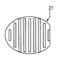
27 犠牲層パターン
28 犠牲層パターン
29 犠牲層パターン
30 犠牲層パターン
31 犠牲層パターン
32 犠牲層パターン
33 犠牲層パターン
34 犠牲層パターン
35 犠牲層パターン
36 窒化物発光装置
37 窒化物発光装置
38 窒化物発光装置
39 窒化物発光装置
40 窒化物発光装置
41 酸化アルミニウム基板
42 粗化表面
43 n型GaN
44 活性層
45 p型GaN
46 p型電極
47 n型電極
50 p型窒化物エピタキシャル層
51 活性層
52 n型窒化物エピタキシャル層
53 光線キャプチャ層
54 酸化アルミニウム基板
55A p型電極
55B n型電極
50’ p型窒化物エピタキシャル層
51’ 活性層
52’ n型窒化物エピタキシャル層
53’ 光線キャプチャ層
54’ 酸化アルミニウム基板
55A’ p型電極
55B’ n型電極
50” p型窒化物エピタキシャル層
51” 活性層
52” n型窒化物エピタキシャル層
53” 光線キャプチャ層
54” 酸化アルミニウム基板
55A” p型電極
55B” n型電極
70 窒化物発光装置
71 p型窒化物エピタキシャル層
72 活性層
73 n型窒化物エピタキシャル層
74 酸化アルミニウム基板
76A’ p型電極
76B’ n型電極
77 透明導電層(TCL)
81 エキシマレーザー
82 サファイヤ
83 犠牲層
84 GaN
85 結合層
86 Si層
90 p型窒化物エピタキシャル層
91 活性層
92 n型窒化物エピタキシャル層
93 犠牲層
94 酸化アルミニウム基板
90’ p型窒化物エピタキシャル層
91’ 活性層
92’ n型窒化物エピタキシャル層
93’ 犠牲層
94’ 酸化アルミニウム基板
100 方法
110 犠牲層製作
120 窒化物エピタキシャル層成長
130 チップ結合
140 ケミカルエッチング
150 リソグラフィー、蒸着、エッチング
160 研磨、切断
170 パッケージ
DESCRIPTION OF
44 Active layer 45 p-type GaN
46 p-type electrode 47 n-type electrode 50 p-type
81
85
Claims (5)
この成長基板の上に成長させた光線キャプチャ層と、
この光線キャプチャ層の上に成長させた窒化物エピタキシャル層と、
を具えた窒化物発光装置において、
該光線キャプチャ層が光線のもとの行進経路を改変することにより、光線がエピタキシャル層により吸収されるのを防止して発光装置より射出されるようにし、これにより発光効率を高め、並びにこの光線キャプチャ層と成長基板の屈折率のマッチングによっても発光効率を高め、
光線キャプチャ層の材料を、ITO(インジウム・スズ酸化物)、酸化インジウム(In 2 O 3 )、二酸化チタン(TiO 2 )、酸化ジルコニウム(Z 2 O 2 )、硫化亜鉛(ZnS)、酸化亜鉛(ZnO)、セレン化亜鉛(ZnSe)、及び酸化マグネシウム(MgO)のいずれかとしたことを特徴とする、窒化物発光装置。 A growth substrate;
A light capture layer grown on the growth substrate;
A nitride epitaxial layer grown on the light capture layer;
In a nitride light emitting device comprising:
The light capture layer modifies the original marching path of the light beam to prevent the light beam from being absorbed by the epitaxial layer and to be emitted from the light emitting device, thereby increasing the light emission efficiency and the light beam. The luminous efficiency is also increased by matching the refractive index of the capture layer and growth substrate ,
The material of the light capture layer is made of ITO (indium tin oxide), indium oxide (In 2 O 3 ), titanium dioxide (TiO 2 ), zirconium oxide (Z 2 O 2 ), zinc sulfide (ZnS), zinc oxide ( A nitride light-emitting device characterized by being any one of ZnO), zinc selenide (ZnSe), and magnesium oxide (MgO) .
Priority Applications (2)
| Application Number | Priority Date | Filing Date | Title |
|---|---|---|---|
| JP2003428067A JP4557542B2 (en) | 2003-12-24 | 2003-12-24 | Nitride light emitting device and high luminous efficiency nitride light emitting device |
| US10/747,934 US20050145872A1 (en) | 2003-12-24 | 2003-12-29 | High performance nitride-based light-emitting diodes |
Applications Claiming Priority (2)
| Application Number | Priority Date | Filing Date | Title |
|---|---|---|---|
| JP2003428067A JP4557542B2 (en) | 2003-12-24 | 2003-12-24 | Nitride light emitting device and high luminous efficiency nitride light emitting device |
| US10/747,934 US20050145872A1 (en) | 2003-12-24 | 2003-12-29 | High performance nitride-based light-emitting diodes |
Related Child Applications (1)
| Application Number | Title | Priority Date | Filing Date |
|---|---|---|---|
| JP2010092184A Division JP2010157772A (en) | 2010-04-13 | 2010-04-13 | Nitride light emitting device and high luminous efficiency nitride light emitting device |
Publications (2)
| Publication Number | Publication Date |
|---|---|
| JP2005191110A JP2005191110A (en) | 2005-07-14 |
| JP4557542B2 true JP4557542B2 (en) | 2010-10-06 |
Family
ID=34840104
Family Applications (1)
| Application Number | Title | Priority Date | Filing Date |
|---|---|---|---|
| JP2003428067A Expired - Lifetime JP4557542B2 (en) | 2003-12-24 | 2003-12-24 | Nitride light emitting device and high luminous efficiency nitride light emitting device |
Country Status (2)
| Country | Link |
|---|---|
| US (1) | US20050145872A1 (en) |
| JP (1) | JP4557542B2 (en) |
Families Citing this family (37)
| Publication number | Priority date | Publication date | Assignee | Title |
|---|---|---|---|---|
| US9929326B2 (en) | 2004-10-29 | 2018-03-27 | Ledengin, Inc. | LED package having mushroom-shaped lens with volume diffuser |
| US8816369B2 (en) | 2004-10-29 | 2014-08-26 | Led Engin, Inc. | LED packages with mushroom shaped lenses and methods of manufacturing LED light-emitting devices |
| US8134292B2 (en) * | 2004-10-29 | 2012-03-13 | Ledengin, Inc. | Light emitting device with a thermal insulating and refractive index matching material |
| US8324641B2 (en) * | 2007-06-29 | 2012-12-04 | Ledengin, Inc. | Matrix material including an embedded dispersion of beads for a light-emitting device |
| US7670872B2 (en) | 2004-10-29 | 2010-03-02 | LED Engin, Inc. (Cayman) | Method of manufacturing ceramic LED packages |
| US7772609B2 (en) | 2004-10-29 | 2010-08-10 | Ledengin, Inc. (Cayman) | LED package with structure and materials for high heat dissipation |
| JP2007134388A (en) * | 2005-11-08 | 2007-05-31 | Sharp Corp | Nitride based semiconductor element and process for fabricating same |
| KR20070081184A (en) | 2006-02-10 | 2007-08-16 | 삼성전기주식회사 | Nitride-based semiconductor light emitting device and method of manufacturing the same |
| TWI309481B (en) * | 2006-07-28 | 2009-05-01 | Epistar Corp | A light emitting device having a patterned substrate and the method thereof |
| KR100755656B1 (en) * | 2006-08-11 | 2007-09-04 | 삼성전기주식회사 | Method of manufacturing nitride-based semiconductor light emitting device |
| JP4381439B2 (en) * | 2007-09-18 | 2009-12-09 | 株式会社沖データ | LED backlight device and liquid crystal display device |
| US20100200880A1 (en) * | 2008-06-06 | 2010-08-12 | Hong Kong Applied Science And Technology Research Institute Co. Ltd. | Semiconductor wafers and semiconductor devices and methods of making semiconductor wafers and devices |
| US8435816B2 (en) * | 2008-08-22 | 2013-05-07 | Lattice Power (Jiangxi) Corporation | Method for fabricating InGaAlN light emitting device on a combined substrate |
| US8075165B2 (en) * | 2008-10-14 | 2011-12-13 | Ledengin, Inc. | Total internal reflection lens and mechanical retention and locating device |
| US20100117106A1 (en) * | 2008-11-07 | 2010-05-13 | Ledengin, Inc. | Led with light-conversion layer |
| US8507300B2 (en) * | 2008-12-24 | 2013-08-13 | Ledengin, Inc. | Light-emitting diode with light-conversion layer |
| US8598793B2 (en) | 2011-05-12 | 2013-12-03 | Ledengin, Inc. | Tuning of emitter with multiple LEDs to a single color bin |
| US7985000B2 (en) * | 2009-04-08 | 2011-07-26 | Ledengin, Inc. | Lighting apparatus having multiple light-emitting diodes with individual light-conversion layers |
| CN101894901B (en) | 2009-04-08 | 2013-11-20 | 硅谷光擎 | Package for multiple light emitting diodes |
| US8303141B2 (en) * | 2009-12-17 | 2012-11-06 | Ledengin, Inc. | Total internal reflection lens with integrated lamp cover |
| US8858022B2 (en) | 2011-05-05 | 2014-10-14 | Ledengin, Inc. | Spot TIR lens system for small high-power emitter |
| US9080729B2 (en) | 2010-04-08 | 2015-07-14 | Ledengin, Inc. | Multiple-LED emitter for A-19 lamps |
| US9345095B2 (en) | 2010-04-08 | 2016-05-17 | Ledengin, Inc. | Tunable multi-LED emitter module |
| US8513900B2 (en) | 2011-05-12 | 2013-08-20 | Ledengin, Inc. | Apparatus for tuning of emitter with multiple LEDs to a single color bin |
| US8686433B2 (en) | 2011-09-01 | 2014-04-01 | Rohm Co., Ltd. | Light emitting device and light emitting device package |
| JP5885436B2 (en) * | 2011-09-06 | 2016-03-15 | ローム株式会社 | Light emitting device and light emitting device package |
| CN103022311A (en) * | 2011-09-27 | 2013-04-03 | 大连美明外延片科技有限公司 | GaN-LED (Light-Emitting Diode) chip structure and preparation method thereof |
| FR2985609B1 (en) * | 2012-01-05 | 2014-02-07 | Commissariat Energie Atomique | STRUCTURAL SUBSTRATE FOR LEDS WITH HIGH LIGHT EXTRACTION |
| US11032884B2 (en) | 2012-03-02 | 2021-06-08 | Ledengin, Inc. | Method for making tunable multi-led emitter module |
| US9897284B2 (en) | 2012-03-28 | 2018-02-20 | Ledengin, Inc. | LED-based MR16 replacement lamp |
| US9234801B2 (en) | 2013-03-15 | 2016-01-12 | Ledengin, Inc. | Manufacturing method for LED emitter with high color consistency |
| US9406654B2 (en) | 2014-01-27 | 2016-08-02 | Ledengin, Inc. | Package for high-power LED devices |
| EP3224874B1 (en) | 2014-11-26 | 2019-04-24 | LedEngin, Inc. | Compact emitter for warm dimming and color tunable lamp |
| US9530943B2 (en) | 2015-02-27 | 2016-12-27 | Ledengin, Inc. | LED emitter packages with high CRI |
| US10219345B2 (en) | 2016-11-10 | 2019-02-26 | Ledengin, Inc. | Tunable LED emitter with continuous spectrum |
| US10575374B2 (en) | 2018-03-09 | 2020-02-25 | Ledengin, Inc. | Package for flip-chip LEDs with close spacing of LED chips |
| US20230420434A1 (en) * | 2020-11-18 | 2023-12-28 | Enkris Semiconductor, Inc. | Semiconductor structure |
Citations (1)
| Publication number | Priority date | Publication date | Assignee | Title |
|---|---|---|---|---|
| JPH11274568A (en) * | 1998-02-19 | 1999-10-08 | Hewlett Packard Co <Hp> | Led and led-assembling method |
Family Cites Families (6)
| Publication number | Priority date | Publication date | Assignee | Title |
|---|---|---|---|---|
| US6071795A (en) * | 1998-01-23 | 2000-06-06 | The Regents Of The University Of California | Separation of thin films from transparent substrates by selective optical processing |
| US6646292B2 (en) * | 1999-12-22 | 2003-11-11 | Lumileds Lighting, U.S., Llc | Semiconductor light emitting device and method |
| TW488088B (en) * | 2001-01-19 | 2002-05-21 | South Epitaxy Corp | Light emitting diode structure |
| TW536841B (en) * | 2001-03-21 | 2003-06-11 | Mitsubishi Cable Ind Ltd | Semiconductor light emitting element |
| US7198671B2 (en) * | 2001-07-11 | 2007-04-03 | Matsushita Electric Industrial Co., Ltd. | Layered substrates for epitaxial processing, and device |
| US6831302B2 (en) * | 2003-04-15 | 2004-12-14 | Luminus Devices, Inc. | Light emitting devices with improved extraction efficiency |
-
2003
- 2003-12-24 JP JP2003428067A patent/JP4557542B2/en not_active Expired - Lifetime
- 2003-12-29 US US10/747,934 patent/US20050145872A1/en not_active Abandoned
Patent Citations (1)
| Publication number | Priority date | Publication date | Assignee | Title |
|---|---|---|---|---|
| JPH11274568A (en) * | 1998-02-19 | 1999-10-08 | Hewlett Packard Co <Hp> | Led and led-assembling method |
Also Published As
| Publication number | Publication date |
|---|---|
| US20050145872A1 (en) | 2005-07-07 |
| JP2005191110A (en) | 2005-07-14 |
Similar Documents
| Publication | Publication Date | Title |
|---|---|---|
| JP4557542B2 (en) | Nitride light emitting device and high luminous efficiency nitride light emitting device | |
| CN104022204B (en) | Light-emitting component | |
| US7067340B1 (en) | Flip-chip light emitting diode and fabricating method thereof | |
| US8519430B2 (en) | Optoelectronic device and method for manufacturing the same | |
| US8704257B2 (en) | Light-emitting element and the manufacturing method thereof | |
| KR101469979B1 (en) | group 3 nitride-based semiconductor light emitting diodes and methods to fabricate them | |
| US20050017254A1 (en) | Light emitting diode and method of making the same | |
| US8022430B2 (en) | Nitride-based compound semiconductor light-emitting device | |
| JP2006324672A (en) | Perpendicular structure nitride semiconductor light emitting device with improved optical extraction efficiency | |
| JP4812369B2 (en) | Method for manufacturing light emitting device | |
| JP2011176093A (en) | Substrate for light-emitting element, and light-emitting element | |
| JP2009059969A (en) | Semiconductor light-emitting element, light-emitting device, luminaire, display unit, and method for fabricating semiconductor light-emitting element | |
| JP2011060966A (en) | Light-emitting device | |
| EP2346096A1 (en) | Semiconductor light-emitting element, manufacturing method, and light-emitting device | |
| US7700966B2 (en) | Light emitting device having vertical structure and method for manufacturing the same | |
| US20170040493A1 (en) | Optoelectronic device | |
| JP2011171327A (en) | Light emitting element, method for manufacturing the same, and light emitting device | |
| JP2009032958A (en) | Light-emitting element and illuminator | |
| US9356189B2 (en) | Light-emitting device and method for manufacturing the same | |
| KR20090105462A (en) | Vertical structured group 3 nitride-based light emitting diode and its fabrication methods | |
| JP2012178453A (en) | GaN-BASED LED ELEMENT | |
| JP2006086254A (en) | Light emitting element, its manufacturing method, and lighting device using the same | |
| JP2006135313A (en) | Light emitting diode | |
| JP4721691B2 (en) | LIGHT EMITTING ELEMENT AND LIGHTING DEVICE USING THE LIGHT EMITTING ELEMENT | |
| JP2010157772A (en) | Nitride light emitting device and high luminous efficiency nitride light emitting device |
Legal Events
| Date | Code | Title | Description |
|---|---|---|---|
| A621 | Written request for application examination |
Free format text: JAPANESE INTERMEDIATE CODE: A621 Effective date: 20061020 |
|
| A131 | Notification of reasons for refusal |
Free format text: JAPANESE INTERMEDIATE CODE: A131 Effective date: 20100119 |
|
| A521 | Request for written amendment filed |
Free format text: JAPANESE INTERMEDIATE CODE: A523 Effective date: 20100413 |
|
| TRDD | Decision of grant or rejection written | ||
| A01 | Written decision to grant a patent or to grant a registration (utility model) |
Free format text: JAPANESE INTERMEDIATE CODE: A01 Effective date: 20100706 |
|
| A01 | Written decision to grant a patent or to grant a registration (utility model) |
Free format text: JAPANESE INTERMEDIATE CODE: A01 |
|
| A61 | First payment of annual fees (during grant procedure) |
Free format text: JAPANESE INTERMEDIATE CODE: A61 Effective date: 20100720 |
|
| R150 | Certificate of patent or registration of utility model |
Ref document number: 4557542 Country of ref document: JP Free format text: JAPANESE INTERMEDIATE CODE: R150 Free format text: JAPANESE INTERMEDIATE CODE: R150 |
|
| FPAY | Renewal fee payment (event date is renewal date of database) |
Free format text: PAYMENT UNTIL: 20130730 Year of fee payment: 3 |
|
| R250 | Receipt of annual fees |
Free format text: JAPANESE INTERMEDIATE CODE: R250 |
|
| R250 | Receipt of annual fees |
Free format text: JAPANESE INTERMEDIATE CODE: R250 |
|
| R250 | Receipt of annual fees |
Free format text: JAPANESE INTERMEDIATE CODE: R250 |
|
| R250 | Receipt of annual fees |
Free format text: JAPANESE INTERMEDIATE CODE: R250 |
|
| S111 | Request for change of ownership or part of ownership |
Free format text: JAPANESE INTERMEDIATE CODE: R313113 |
|
| R360 | Written notification for declining of transfer of rights |
Free format text: JAPANESE INTERMEDIATE CODE: R360 |
|
| R360 | Written notification for declining of transfer of rights |
Free format text: JAPANESE INTERMEDIATE CODE: R360 |
|
| R360 | Written notification for declining of transfer of rights |
Free format text: JAPANESE INTERMEDIATE CODE: R360 |
|
| R371 | Transfer withdrawn |
Free format text: JAPANESE INTERMEDIATE CODE: R371 |
|
| S111 | Request for change of ownership or part of ownership |
Free format text: JAPANESE INTERMEDIATE CODE: R313113 |
|
| S531 | Written request for registration of change of domicile |
Free format text: JAPANESE INTERMEDIATE CODE: R313531 |
|
| R350 | Written notification of registration of transfer |
Free format text: JAPANESE INTERMEDIATE CODE: R350 |
|
| R250 | Receipt of annual fees |
Free format text: JAPANESE INTERMEDIATE CODE: R250 |
|
| R250 | Receipt of annual fees |
Free format text: JAPANESE INTERMEDIATE CODE: R250 |
|
| R250 | Receipt of annual fees |
Free format text: JAPANESE INTERMEDIATE CODE: R250 |
|
| R250 | Receipt of annual fees |
Free format text: JAPANESE INTERMEDIATE CODE: R250 |
|
| R250 | Receipt of annual fees |
Free format text: JAPANESE INTERMEDIATE CODE: R250 |
|
| R250 | Receipt of annual fees |
Free format text: JAPANESE INTERMEDIATE CODE: R250 |
|
| R250 | Receipt of annual fees |
Free format text: JAPANESE INTERMEDIATE CODE: R250 |
|
| EXPY | Cancellation because of completion of term |