JP2004335864A - Aligner and exposure method - Google Patents
Aligner and exposure method Download PDFInfo
- Publication number
- JP2004335864A JP2004335864A JP2003131781A JP2003131781A JP2004335864A JP 2004335864 A JP2004335864 A JP 2004335864A JP 2003131781 A JP2003131781 A JP 2003131781A JP 2003131781 A JP2003131781 A JP 2003131781A JP 2004335864 A JP2004335864 A JP 2004335864A
- Authority
- JP
- Japan
- Prior art keywords
- light
- exposure
- mask
- blind
- substrate
- Prior art date
- Legal status (The legal status is an assumption and is not a legal conclusion. Google has not performed a legal analysis and makes no representation as to the accuracy of the status listed.)
- Withdrawn
Links
Images


Landscapes
- Exposure And Positioning Against Photoresist Photosensitive Materials (AREA)
- Exposure Of Semiconductors, Excluding Electron Or Ion Beam Exposure (AREA)
Abstract
Description
【0001】
【発明の属する技術分野】
本発明は、マスクと基板とを同期移動しつつマスクのパターンを基板に露光する露光装置及び露光方法に関するものである。
【0002】
【従来の技術】
液晶表示デバイスや半導体デバイスは、マスク上に形成されたパターンを感光基板上に転写する、いわゆるフォトリソグラフィの手法により製造される。このフォトリソグラフィ工程で使用される露光装置は、感光基板を載置して2次元移動する基板ステージとパターンを有するマスクを載置して2次元移動するマスクステージとを有し、マスク上に形成されたパターンをマスクステージ及び基板ステージを逐次移動しながら投影光学系を介して感光基板に転写するものである。そして、露光装置としては、感光基板上にマスクのパターン全体を同時に転写する一括型露光装置と、マスクステージと基板ステージとを同期走査しつつマスクのパターンを連続的に感光基板上に転写する走査型露光装置との2種類が主に知られている。このうち、液晶表示デバイスを製造する際には、表示領域の大型化の要求から走査型露光装置が主に用いられている(特許文献1参照)。
【0003】
走査型露光装置には、複数の投影光学系を、隣り合う投影領域が走査方向で所定量変位するように、且つ隣り合う投影領域の端部どうしが走査方向と直交する方向に重複するように配置した、いわゆるマルチレンズ方式の走査型露光装置(マルチレンズスキャン型露光装置)がある。マルチレンズ方式の走査型露光装置は、良好な結像特性を維持しつつ、装置を大型化せずに大きな露光領域を得ることができる。上記走査型露光装置における各投影光学系の視野絞りは、例えば台形形状で、走査方向の視野絞りの開口幅の合計は常に等しくなるように設定されている。そのため、隣り合う投影光学系の継ぎ部が重複して露光されるので、上記走査型露光装置は、投影光学系の光学収差や露光照度が滑らかに変化するという利点を有している。
【0004】
そして、走査型露光装置においては、マスクと感光基板とを同期移動して走査露光を行った後に、これらマスクと感光基板とを走査方向と直交する方向にステップ移動し、複数回の走査露光を行ってパターンの一部を重複させて露光し、これらパターンを継ぎ合わせて合成することにより、大きな表示領域を有する液晶表示デバイスを製造している。
【0005】
走査露光とステップ移動とを繰り返すことにより感光基板上でパターン合成を行う方法としては、例えば、マスクに複数の分割パターンを形成しておき、これら分割パターンを感光基板上で継ぎ合わせる方法や、マスクのパターン像を複数の投影領域に分割し、これら分割した投影領域を感光基板上で継ぎ合わせる方法などがある。前者の方法は、例えば図31に示すように、マスクMに3つの分割パターンPa、Pb、Pcを形成しておき、これら各分割パターンPa、Pb、Pcを感光基板Pに順次露光し、感光基板P上で継ぎ合わせる方法である。
【0006】
一方、後者の方法は、例えば図32に示すように、マスクMに形成されているパターンに対する露光光の照射領域を走査露光毎に変更し、これら照射領域に対応する投影領域で感光基板P上に順次走査露光し、パターン合成を行うものである。ここで、投影光学系は5つ設けられ、図32(a)に示すように、それぞれの投影領域100a〜100eは台形形状に設定されており、走査方向(X軸方向)の積算露光量が常に等しくなるように、それぞれの端部をY軸方向に重ね合わせるように配置され、X軸方向の投影領域の幅の総計が等しくなるように設定されている。そして、感光基板Pにパターンを露光する際には、複数の投影領域100a〜100eのうち、所定の投影領域に対応する光路をシャッタで遮光してマスクMの所定の領域のみが露光光で照射されるようにし、複数回の走査露光において投影領域の端部どうしが重複するように露光する。具体的には、図32(b)に示すように、一回目の走査露光における投影領域100dの−Y側の端部a1と、二回目の走査露光における投影領域100bの+Y側の端部a2とが重複するように露光される。同様に、二回目の走査露光における投影領域100cの−Y側の端部a3と、三回目の走査露光における投影領域100bの+Y側の端部a4とが重複するように露光される。このとき、一回目の走査露光においては投影領域100eが遮光され、二回目の走査露光においては投影領域100a、100d、100eが遮光され、三回目の走査露光においては投影領域100aが遮光される。
【0007】
ここで、一回目の走査露光によって感光基板P上に形成される分割パターンのY軸方向の長さL12は、投影領域100aの短辺の+Y方向端点と投影領域100dの長辺の−Y方向端点との間のY軸方向における距離である。二回目の走査露光によって感光基板P上に形成される分割パターンのY軸方向の長さL13は、投影領域100bの長辺の+Y方向端点と投影領域100cの長辺の−Y方向端点との間のY軸方向における距離である。三回目の走査露光によって感光基板P上に形成される分割パターンのY軸方向の長さL14は、投影領域100bの長辺の+Y方向端点と投影領域100eの短辺の−Y方向端点との間のY軸方向における距離である。このように、それぞれの分割パターンのサイズ(Y軸方向の長さL12、L13、L14)は、台形形状の投影領域の長辺及び短辺のサイズに基づくものである。
【0008】
【特許文献1】
特開2001−296667号公報
【0009】
【発明が解決しようとする課題】
しかしながら、上述したような従来の走査型露光方法及び走査型露光装置には、以下のような問題が存在する。
図31に示した方法では、マスクM上に複数の独立した分割パターンを形成するため、マスクM上におけるパターン構成に制約がある。更に、分割パターン毎に走査露光を行うため、走査露光回数が増加し、スループットが低下する。
【0010】
また、図32に示した方法では、複数回の走査露光によってパターン合成を行う際、上述したように、それぞれの分割パターンのサイズ(Y軸方向の長さL12、L13、L14)は、台形形状の投影領域の長辺及び短辺のサイズに基づくものである。すなわち、図32に示した方法では、感光基板P上に形成されるパターンの大きさは投影領域の大きさ、ひいては視野絞りの大きさ(形状)によって限定されてしまう。更に、分割パターンの継ぎ合わせは、台形形状の投影領域の端部のみにおいて行われるので、パターンの分割位置も限定される。このように、従来の方法では、パターンの分割位置や、感光基板P上に形成されるパターンの大きさが限定されてしまい、任意のデバイス作成が困難となる。
【0011】
本発明はこのような事情に鑑みてなされたもので、分割パターンの一部を重複させつつ感光基板上で継ぎ合わせて露光する際、感光基板に形成されるパターンの大きさを任意に設定できるとともに、マスク上におけるパターンの分割位置を任意に設定でき、効率良いデバイス製造を実現できる露光装置及び露光方法を提供することを目的とする。
【0012】
【課題を解決するための手段】
上記の課題を解決するため本発明は、実施の形態に示す図1〜図30に対応付けした以下の構成を採用している。
本発明の露光装置(EX)は、マスク(M)と基板(P)とを第1の方向(X)に同期移動しつつマスク(M)を露光光(EL)で照明し、先に基板(P)上に転写されたマスク(M)のパターン像(50a〜50g、62)に対して次に転写するマスク(M)のパターン像(50a〜50g、63)の一部を重複するように露光する露光装置において、基板(P)上に転写されるパターン像(50a〜50g)の第1の方向(X)における幅(Lx)を設定する視野絞り(20)と、パターン像(50a〜50g)の第1の方向(X)と直交する第2の方向(Y)における幅(Ly)を設定する第1遮光部材(40)と、パターン像(50a〜50g)の重複領域(48、49、64)を設定するとともに、パターン像(50a〜50g)の重複領域(48、49、64)の積算露光量をパターン像(50a〜50g)の周辺に向かうに従い漸次減衰させる減光部(30A、30B)を有する第2遮光部材(30)とを有し、減光部(30A、30B)は、第2遮光部材(30)の少なくとも2箇所に設けられていることを特徴とする。
本発明の露光方法は、マスク(M)と基板(P)とを第1の方向(X)に同期移動しつつマスク(M)を露光光(EL)で照明し、先に基板(P)上に転写されたマスク(M)のパターン像(50a〜50g、62)に対して次に転写するマスク(M)のパターン像(50a〜50g、63)の一部を重複するように露光する露光方法において、基板(P)上に転写されるパターン像(50a〜50g)の第1の方向(X)における幅(Lx)を視野絞り(20)で設定し、パターン像(50a〜50g)の第1の方向(X)と直交する第2の方向(Y)における幅(Ly)を第1遮光部材(40)で設定し、パターン像(50a〜50g)の重複領域(48、49、64)の積算露光量をパターン像(50a〜50g)の周辺に向かうに従い漸次減衰させる減光部(30A、30B)を少なくとも2箇所に有する第2遮光部材(30)でパターン像(50a〜50g)の重複領域(48、49、64)を設定することを特徴とする。
【0013】
本発明によれば、視野絞り及び第1遮光部材によって、基板(感光基板)上におけるパターン像の第1の方向及び第1の方向と直交する第2の方向の幅を設定し、この設定されたパターン像を基板上で継ぎ合わせる際、第2遮光部材を所定の位置に配置することにより、基板に対して露光光が照射される領域(投影光学系を備えた露光装置の場合は基板上での投影領域)を任意に設定できる。したがって、パターン像の継ぎ部分である重複領域を任意に設定でき、基板に形成されるパターンの大きさを任意に設定できる。また、第2遮光部材には、パターン像の重複領域の積算露光量をパターン像の周辺に向かうに従い漸次減衰させる減光部が少なくとも2箇所に設けられているので、2箇所の減光部のうちいずれか一方の減光部を使って重複領域の位置や露光量を所望の状態に設定でき、重複領域と重複領域以外との露光量を一致させることができる。したがって、精度良い露光処理を行うことができる。そして、第2遮光部材を任意の位置に移動することにより、基板に対する露光光の照射領域の大きさや形状を任意に設定でき、継ぎ露光する際の継ぎ合わせ精度の向上や、露光量の均一化を実現できる。
【0014】
【発明の実施の形態】
以下、本発明の露光装置について図面を参照しながら説明する。図1は本発明の露光装置の一実施形態を示す概略斜視図である。
図1において、露光装置EXは、マスクMを支持するマスクステージMSTと、感光基板(基板)Pを支持する基板ステージPSTと、マスクステージMSTに支持されているマスクMを露光光ELで照明する照明光学系ILと、露光光ELで照明されたマスクMのパターン像を基板ステージPSTに支持されている感光基板Pに投影露光する投影光学系PLと、露光装置EXの動作を統括制御する制御装置CONTとを備えている。感光基板Pはガラスプレート(ガラス基板)に感光剤(フォトレジスト)を塗布したものである。投影光学系PLは複数(7つ)の投影光学モジュールPLa〜PLgにより構成され、本実施形態における露光装置EXは、この投影光学系PL(PLa〜PLg)に対してマスクMと感光基板Pとを所定方向(第1の方向)に同期移動しつつマスクMを露光光ELで照明し、マスクMのパターン像を感光基板Pに露光する、所謂マルチレンズスキャン型露光装置である。
【0015】
ここで、以下の説明において、マスクMと感光基板Pとの同期移動方向(走査方向、第1の方向)をX軸方向、水平面内において前記走査方向と直交する方向をY軸方向(非走査方向、第2の方向)、X軸方向及びY軸方向に直交する方向をZ軸方向とする。また、X軸、Y軸、及びZ軸の軸線まわり方向を、それぞれθX、θY、及びθZ方向とする。
【0016】
マスクMを支持するマスクステージMSTは、一次元の走査露光を行うべくX軸方向に長いストロークと、走査方向と直交するY軸方向に所定距離のストロークとを有している。また、マスクステージMSTはZ軸方向及びθZ方向にも微動可能である。マスクステージMSTは、このマスクステージMSTを移動するリニアモータ等により構成されるマスクステージ駆動部MSTDを備えている。マスクステージ駆動部MSTDは制御装置CONTにより制御される。マスクステージMST上のX軸及びY軸方向のそれぞれの端縁には、直交する方向に移動鏡32a、32bがそれぞれ設置されている。移動鏡32aにはレーザ干渉計33aが対向して配置され、移動鏡32bにはレーザ干渉計33bが対向して配置されている。これらレーザ干渉計33a、33bは移動鏡32a、32bのそれぞれにレーザ光を照射し、移動鏡32a、32bとの間の距離を計測することにより、マスクステージMSTのX軸及びY軸方向の位置、すなわちマスクMの位置を高分解能、高精度に検出可能となっている。レーザ干渉計33a、33bの検出結果は制御装置CONTに出力される。制御装置CONTはレーザ干渉計33a、33bの出力からマスクステージMSTの位置をモニタし、マスクステージ駆動部MSTDを制御することでマスクステージMSTを所望の位置へ移動する。
【0017】
マスクMを透過した露光光ELは、投影光学系PL(投影光学モジュールPLa〜PLg)にそれぞれ入射する。この投影光学モジュールPLa〜PLgは、マスクMの照射範囲に存在するパターン像を感光基板Pに結像させ、感光基板Pの特定領域にパターン像を投影露光するものである。投影光学モジュールPLa〜PLgのそれぞれは定盤150に支持されており、定盤150は不図示のコラムに支持されている。複数の投影光学モジュールPLa〜PLgのうち、投影光学モジュールPLa、PLc、PLe、PLgと投影光学モジュールPLb、PLd、PLfとが2列に千鳥状に配列されている。各投影光学モジュールPLa〜PLgを透過した露光光ELは、感光基板P上の異なる投影領域50a〜50gにマスクMの照射領域に対応したパターン像を所定の結像特性で結像する。
【0018】
感光基板Pを支持する基板ステージPSTは基板ホルダPHを有しており、この基板ホルダPHを介して感光基板Pを保持する。基板ステージPSTは、マスクステージMSTと同様に、一次元の走査露光を行うべくX軸方向に長いストロークと、走査方向と直交するY軸方向にステップ移動するための長いストロークとを有している。また、基板ステージ駆動部PSTDは制御装置CONTによって制御される。基板ステージPSTはZ軸方向にも移動可能であり、更に、θX、θY、及びθZ方向にも移動可能である。そして、基板ステージPSTは、この基板ステージPSTを移動するリニアモータ等により構成される基板ステージ駆動部PSTDを備えている。
【0019】
基板ステージPST上のX軸及びY軸方向のそれぞれの端縁には、直交する方向に移動鏡34a、34bがそれぞれ設置されている。移動鏡34aにはレーザ干渉計35aが対向して配置され、移動鏡34bにはレーザ干渉計35bが対向して配置されている。これらレーザ干渉計35a、35bのそれぞれは、移動鏡34a、34bにレーザ光を照射してこれら移動鏡34a、34bとの間の距離を計測することにより、基板ステージPSTのX軸及びY軸方向の位置、すなわち感光基板Pの位置を高分解能、高精度に検出可能となっている。レーザ干渉計35a、35bの検出結果は制御装置CONTに出力される。制御装置CONTは、レーザ干渉計35a、35bの出力から基板ステージPSTの位置をモニターし、基板ステージ駆動部PSTDを制御することで基板ステージPSTを所望の位置へ移動可能となっている。
【0020】
また、−X側の投影光学モジュールPLa、PLc、PLe、PLgと、+X側の投影光学モジュールPLb、PLd、PLfとの間には、マスクMのパターン面及び感光基板Pの露光面のZ軸方向における位置を検出するフォーカス検出系110が設けられている。フォーカス検出系110を構成する光学素子はハウジング内部に配置されており、これら光学素子及びハウジングによりオートフォーカスユニット(AFユニット)Uが形成されている。フォーカス検出系110は、例えば、斜入射方式の焦点検出系の1つである多点フォーカス位置検出系によって構成される。フォーカス検出系110の検出結果は制御装置CONTに出力され、制御装置CONTは、フォーカス検出系110の検出結果に基づいて、マスクMのパターン面と感光基板Pの露光面とが常に所定の間隔になるように位置制御する。
【0021】
マスクステージ駆動部MSTD及び基板ステージ駆動部PSTDは制御装置CONTによりそれぞれ独立して制御され、マスクステージMST及び基板ステージPSTは、マスクステージ駆動部MSTD及び基板ステージ駆動部PSTDのそれぞれの駆動のもとでそれぞれ独立して移動可能となっている。そして、制御装置CONTは、マスクステージMST及び基板ステージPSTの位置をモニタしながら、両駆動部PSTD、MSTDを制御することにより、マスクMと感光基板Pとを投影光学系PLに対して、任意の走査速度(同期移動速度)でX軸方向に同期移動するようになっている。ここで、マスクステージMSTに支持されているマスクMと、基板ステージPSTに支持されている感光基板Pとは、投影光学系PLを介して共役な位置関係に配置される。
【0022】
図2(a)は定盤150に支持されている投影光学系PL(PLa〜PLg)を示す側面図である。
図2(a)に示すように、投影光学系PLを構成する複数の投影光学モジュールPLa〜PLgは定盤150に支持されている。定盤150は、不図示のコラム(支持構造体)にキネマティックに支持されている。複数の投影光学モジュールPLa〜PLgのうち投影光学モジュールPLa、PLc、PLe、PLgがY軸方向に並んで配置され、投影光学モジュールPLb、PLd、PLfがY軸方向に並んで配置されている。また、Y軸方向に並んだ投影光学モジュールPLa、PLc、PLe、PLgと、Y軸方向に並んだ投影光学モジュールPLb、PLd、PLfとはX軸方向において対向するように配置されており、全体で千鳥状に配置されている。千鳥状に配置されている投影光学モジュールPLa〜PLgのそれぞれは、隣合う投影光学モジュールどうし(例えば投影光学モジュールPLaとPLb、PLbとPLc)をY軸方向に所定量変位させて配置されている。
【0023】
定盤150は、例えばメタルマトリクス複合材(MMC:Metal Matrix Composites)により形成されている。メタルマトリクス複合材は金属をマトリクス材としてその中にセラミックス強化材を複合した複合材であり、ここでは金属としてアルミニウムを含むものが用いられている。定盤150の中央部には開口部150Aが形成されており、この開口部150Aにより投影光学モジュールPLa〜PLgそれぞれの露光光ELの光路が確保されている。ここで、定盤150は平面視において左右対称な六角形状(ホームベース状)に形成されており(図1参照)、Y軸方向に4つ並んだ投影光学モジュールPLa、PLc、PLe、PLgは定盤150の幅の広い部分で支持され、Y軸方向に3つ並んだ投影光学モジュールPLb、PLd、PLfは定盤150の幅の狭い部分で支持されている。すなわち、複数並んだ投影光学モジュールの数に応じて定盤150の形状が設定されており、これにより、投影光学モジュールPLa〜PLgを支持するのに十分な強度を得られる範囲において、使用材料が最小限に抑えられている。
【0024】
投影光学モジュールPLa〜PLgのそれぞれは、鏡筒PKと、鏡筒PKの内部に配置されている複数の光学素子(レンズ)とを有している。そして、投影光学モジュールPLa〜PLgのそれぞれは、定盤150に対して互いに独立して接続されており、又分離可能である。これにより、投影光学モジュールをモジュール単位で増減させることが可能となり、その場合において、投影光学モジュールの定盤150に対する取り付け・取り外し作業を容易に行うことができる。更に、投影光学モジュールPLa〜PLgのそれぞれを定盤150に対して互いに独立して接続及び分離可能としたことにより、定盤150の所定の基準位置(例えば開口部150Aの中心位置)に対してそれぞれ独立して位置決め可能であり、各投影光学モジュールPLa〜PLgの互いの相対位置を任意に設定することができる。
【0025】
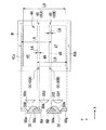
投影光学系PLは、感光基板P上に転写されるマスクMのパターン像の走査方向(X軸方向)の幅を設定する視野絞り20と、視野絞り20とほぼ同じ位置に設けられ感光基板P上に転写されるマスクMのパターン像の非走査方向(Y軸方向)の幅を設定する遮光板(第1遮光部材)40と、感光基板P上に転写されるパターン像の重複領域を設定するブラインド(第2遮光部材)30とを備えている。これら視野絞り20、遮光板40、及びブラインド30は、マスクM及び感光基板Pに対してほぼ共役な位置に配置されており、定盤150に取り付けられたブラインドユニット120内に配置されている。ここで、ブラインドユニット120は、−X側の投影光学モジュールPLa、PLc、PLe、PLgと、+X側の投影光学モジュールPLb、PLd、PLfとのそれぞれに対応するように1つずつ、合計2つ設けられている。
【0026】
視野絞り20及び遮光板40は、各投影光学モジュールPLa〜PLgのそれぞれに設けられており、これら視野絞り20及び遮光板40により形成される開口Kによって、感光基板P上における投影領域50a〜50gのそれぞれの大きさ及び形状が設定される。本実施形態において、視野絞り20及び遮光板40により形成される投影領域50a〜50g(開口K)のそれぞれは平面視台形形状に設定される。一方、ブラインド30は、2つのブラインドユニット120のそれぞれに1つずつ設けられている。すなわち、ブラインド30は、−X側の投影光学モジュールPLa、PLc、PLe、PLgと、+X側の投影光学モジュールPLb、PLd、PLfとのそれぞれに対応するように1つずつ、合計2つ設けられている。
【0027】
図2(b)は、ブラインドユニット120を示す平面図である。ブラインドユニット120内において、各投影光学モジュールPLa〜PLgのそれぞれに設けられた視野絞り20遮光板40により、複数の開口Kが形成されている。ブラインド30は各ブラインドユニット120のそれぞれに1つずつ設けられている。ブラインドユニット120には、ブラインド30を、パターン像の像面と平行な平面内、本実施形態ではXY平面内で移動するブラインド駆動装置31が設けられている。ブラインド駆動装置31はリニアモータ等により構成されており、ガイド部31Aに沿ってブラインド30をY軸方向に長いストロークで移動可能であるとともに、X軸方向に関しても移動可能である。更に、ブラインド駆動装置31は回転機構31Bを有しており、ブラインド30はパターン像の像面と平行な平面内(XY平面内)で回転可能、つまりθZ方向に回転可能である。そして、ブラインド30はブラインド駆動装置31によりY軸方向に移動されることにより、複数の投影光学モジュールPLa〜PLgの間を移動可能となっている。本実施形態では、2つのブラインド30のうち一方(−X側)のブラインド30が投影光学モジュールPLa、PLc、PLe、PLgの間を移動可能であり、他方(+X側)のブラインド30が投影光学モジュールPLb、PLd、PLfの間を移動可能である。
【0028】
図3は露光装置EX全体の概略構成図である。図3に示すように、照明光学系ILは、超高圧水銀ランプ等からなる光源1と、光源1から射出された光束を集光する楕円鏡1aと、この楕円鏡1aによって集光された光束のうち露光に必要な波長の光束を反射し、その他の波長の光束を透過させるダイクロイックミラー2と、ダイクロイックミラー2で反射した光束のうち更に露光に必要な波長(通常は、g、h、i線のうち少なくとも1つの帯域)のみを通過させる波長選択フィルタ3と、波長選択フィルタ3からの光束を複数本(本実施形態では7本)に分岐して、反射ミラー5を介して各照明系モジュールIMa〜IMgに入射させるライトガイド4とを備えている。ここで、照明系モジュールIM(IMa〜IMg)は、複数設けられており、本実施形態では、投影光学モジュールPLa〜PLgに対応して7つ設けられている。但し、図3においては、便宜上照明系モジュールIMfに対応するもののみが示されている。そして、照明光学系IMa〜IMgのそれぞれは、X軸方向とY軸方向とに一定の間隔を持って、投影光学モジュールPLa〜PLgのそれぞれに対応して配置されている。これら複数の照明系モジュールIMa〜IMgのそれぞれから射出した露光光ELは、マスクM上の異なる小領域(照明光学系ILの照明領域)をそれぞれ照明する。
【0029】
照明系モジュールIMa〜IMgのそれぞれは、照明シャッタ6と、リレーレンズ7と、オプティカルインテグレータとしてのフライアイレンズ8と、コンデンサレンズ9とを備えている。照明シャッタ6は、ライトガイド4の光路下流側に、光路に対して進退自在に配置されている。照明シャッタ6は、光路に配置されたときに光束を遮光し、光路から退避したときに遮光を解除する。照明シャッタ6には、この照明シャッタ6を光束の光路に対して進退移動させるシャッタ駆動部6aが接続されている。シャッタ駆動部6aは制御装置CONTによって制御される。
【0030】
また、照明系モジュールIMa〜IMgのそれぞれには光量調整機構10が設けられている。この光量調整機構10は、光路毎に光束の照度を設定することによって各光路の露光量を調整するものであって、ハーフミラー11と、ディテクタ12と、フィルタ13と、フィルタ駆動部14とを備えている。ハーフミラー11は、フィルタ13とリレーレンズ7との間の光路中に配置され、フィルタ13を透過した光束の一部をディテクタ12へ入射させる。それぞれのディテクタ12は、常時、入射した光束の照度を独立して検出し、検出した照度信号を制御装置CONTへ出力する。
【0031】
図4に示すように、フィルタ13は、ガラス板13a上にCr等ですだれ状にパターンニングされたものであって、透過率がX軸方向に沿ってある範囲で線形に漸次変化するように形成されており、各光路中の照明シャッタ6とハーフミラー11との間に配置されている。
【0032】
図3に戻って、これらハーフミラー11、ディテクタ12及びフィルタ13は、複数の光路毎にそれぞれ配設されている。フィルタ駆動部14は、制御装置CONTの指示に基づいてフィルタ13をX軸方向に沿って移動する。そして、フィルタ13をフィルタ駆動部14によって移動することにより、各光路毎の光量が調整される。
【0033】
光量調整機構10を透過した光束はリレーレンズ7を介してフライアイレンズ8に達する。フライアイレンズ8は射出面側に二次光源を形成し、コンデンサレンズ9を介してマスクMの照射領域を均一な照度で照射することができる。そして、コンデンサレンズ9を通過した露光光ELは、照明系モジュールのうち、直角プリズム16と、レンズ系17と、凹面鏡18とを備えた反射屈折型光学系15を通過した後、マスクMを所定の照明領域で照明する。マスクMは、照明系モジュールIMa〜IMgを透過した各露光光ELによって異なる照明領域でそれぞれ照明される。
【0034】
投影光学モジュールPLa〜PLgのそれぞれは、像シフト機構19と、2組の反射屈折型光学系21、22と、視野絞り20と、視野絞り20とほぼ同じ位置に設けられた遮光板(第1遮光部材)40及びブラインド(第2遮光部材)30と、倍率調整機構23とを備えている。像シフト機構19は、例えば、2枚の平行平面板ガラスがそれぞれθY方向もしくはθX方向に回転することで、マスクMのパターン像をX軸方向もしくはY軸方向にシフトさせる。マスクMを透過した露光光ELは像シフト機構19を透過した後、1組目の反射屈折型光学系21に入射する。
【0035】
反射屈折型光学系21は、マスクMのパターンの中間像を形成するものであって、直角プリズム24とレンズ系25と凹面鏡26とを備えている。直角プリズム24はθZ方向に回転自在となっており、マスクMのパターン像を回転可能となっている。
【0036】
この中間像位置に視野絞り20が配置されている。視野絞り20は、感光基板P上での投影領域50a〜50gを設定するものであって、特に、感光基板P上におけるパターン像の走査方向(X軸方向)の幅を設定する。視野絞り20を透過した光束は、2組目の反射屈折型光学系22に入射する。反射屈折型光学系22は、反射屈折型光学系21と同様に、直角プリズム27とレンズ系28と凹面鏡29とを備えている。直角プリズム27もθZ方向に回転自在となっており、マスクMのパターン像を回転可能となっている。つまり、直角プリズム24、27により像ローテーション機構が構成されている。
【0037】
反射屈折型光学系22から射出した露光光ELは、倍率調整機構23を通過し、感光基板P上にマスクMのパターン像を正立等倍で結像する。倍率調整機構23は、例えば、平凸レンズ、両凸レンズ、平凸レンズの3枚のレンズから構成され、平凸レンズと平凹レンズとの間に位置する両凸レンズをZ軸方向に移動させることにより、マスクMのパターン像の倍率を変化させる。
【0038】
次に、視野絞り20、遮光板(第1遮光部材)40及びブラインド(第2遮光部材)30について、図5及び図6を参照しながら説明する。図5及び図6は、視野絞り20、遮光板40、ブラインド30のそれぞれと、投影光学系PL、マスクM、感光基板Pのそれぞれとの位置関係を示した模式図である。
図5には投影光学モジュールPLeが代表して示されており、視野絞り20は投影光学モジュールPLeに配置されており、スリット状の開口を有している。この視野絞り20は、感光基板P上における投影領域50(50e)の形状を設定するものであって、特に、パターン像としての投影領域50の走査方向(X軸方向)の幅Lxを設定するものである。視野絞り20は、投影光学系PL(PLe)のうち、マスクMと感光基板Pとに対してほぼ共役な位置関係に配置されている。
【0039】
遮光板(第1遮光部材)40も、感光基板P上における投影領域50の形状を設定するものであって、特に、パターン像としての投影領域50の非走査方向(Y軸方向)の幅Lyを設定するものである。遮光板40も投影光学モジュールPLeに設けられ、視野絞り20と重なり合うように配置されており、視野絞り20と遮光板40とによって形成される開口Kによって、感光基板P上における投影領域50の大きさ及び形状が設定される。本実施形態において、視野絞り20及び遮光板40によって形成される投影領域50は、平面視台形形状に設定される。ここで、視野絞り20に重なり合うように配置されている遮光板40も、投影光学系PL(PLe)のうち、マスクMと感光基板Pとに対してほぼ共役な位置関係に配置されている。
【0040】
遮光板40には遮光板用駆動機構(不図示)が設けられており、遮光板40は、遮光板用駆動機構の駆動のもとで、非走査方向(Y軸方向)に移動可能となっている。そして、遮光板40をY軸方向に移動することにより、例えば投影領域50eのY軸方向の幅Lyが任意に設定可能となっている。なお、遮光板40は固定されていてもよいが、移動することにより、投影領域50の設定の自由度が増す。
【0041】
ブラインド(第2遮光部材)30は、図2等に示したように、定盤150(投影光学系PL)に取り付けられたブラインドユニット120に設けられており、ブラインド駆動装置31によって複数の投影光学モジュールの間を移動可能となっている。ブラインド駆動装置31の駆動は制御装置CONTにより制御され、制御装置CONTはブラインド30を任意の位置に移動する。そして、ブラインド30は、図6に示すように、Y軸方向に移動することによって、視野絞り20と遮光板40とで形成される開口Kの一部を遮光し(なお、図6では、見やすいように開口Kのみが図示されており、視野絞り20及び遮光板40は図示されていない)、投影領域50の大きさ及び形状を任意に設定する。
【0042】
ブラインド30は、平面視台形状の板部材であって、そのY軸方向両端部30A、30BにおけるX軸方向の幅がY軸方向に向かって漸次縮小するように斜めに形成されている。換言すれば、ブラインド部30のY軸方向の互いに対向する辺が斜めになるように形成されている。そして、この斜め部(減光部)30A、30Bによって露光光ELを遮光することにより、投影領域50の形状が設定される。本実施形態において、視野絞り20と遮光板40とブラインド30とによって形成される投影領域50は、台形形状(平行四辺形形状)に設定される。
【0043】
ブラインド30は、投影光学PLのうち、マスクMと感光基板Pとに対してほぼ共役な位置関係に配置されている。すなわち、本実施形態において、視野絞り20と遮光板40とブラインド30とは、投影光学系PLを介して共役な位置関係に配置されているマスクMと感光基板Pとに対して、ほぼ共役な位置関係に配置されている。
【0044】
本実施形態において、ブラインド30は投影光学系PLの中間像位置に配置されており、図6に示すように、ブラインド30により中間像の−Y側を遮光することで、感光基板P上でのパターン像はその+Y側を遮光される。
【0045】
なお、視野絞り20と遮光板40とブラインド30とは、マスクMと感光基板Pとに対して、共役な位置関係に配置されていればよく、したがって、例えば図7に示すように、遮光板(第1遮光部材)40を照明光学系ILに配置してもよい。あるいは、ブラインド30を照明光学系ILに配置してもよい。あるいは、これら各部材20,30,40をマスクM又は感光基板Pに近接する位置に配置してもよい。すなわち、視野絞り20、遮光板40、ブラインド30のそれぞれは、マスクMと感光基板Pとに対して共役な位置(図3の符号A、B参照)であれば、露光光ELの光路上のいずれの位置に配置してもよい。また、ブラインド30は、共役面に対してデフォーカスした位置に配置しても光量和は一定になるので、フォーカス方向にずれた位置でも構わない。
【0046】
なお、図8に示すように、ブラインド30をθZ方向に回転することにより、投影領域50の形状を変更可能である。同様に、遮光板40をθZ方向に回転移動可能に設け、遮光板40をθZ方向に回転することでも投影領域50の形状を変更可能である。
【0047】
図9は、感光基板P上での投影光学モジュールPLa〜PLgの投影領域50a〜50gの平面図である。各投影領域50a〜50gは、視野絞り20及び遮光板40によって所定の形状(本実施形態では台形形状)に設定される。投影領域50a、50c、50e、50gと、投影領域50b、50d、50fとは、X軸方向に対向して配置されている。さらに、投影領域50a〜50gは、隣り合う投影領域の端部(境界部)どうし(51aと51b、51cと51d、51eと51f、51gと51h、51iと51j、51kと51l)が二点鎖線で示すように、Y軸方向に重なり合うように並列配置され、重複領域(継ぎ部)52a〜52fを形成する。そして、投影領域50a〜50gの境界部どうしをY軸方向に重なり合うように並列配置することにより、X軸方向の投影領域の幅の総計がほぼ等しくなるように設定されている。こうすることにより、X軸方向に走査露光したときの露光量が等しくなるようになっている。
【0048】
このように、各投影光学モジュールPLa〜PLgによる投影領域50a〜50gのそれぞれが重なり合う重複領域(継ぎ部)52a〜52fを設けることにより、継ぎ部52a〜52fにおける光学収差の変化や照度変化を滑らかにすることができる。ここで、継ぎ部52a〜52fのY軸方向における位置や幅は、遮光板40を移動することによって任意に設定可能である。
【0049】
また、図9の破線で示すように、2つのブラインド30のうち、一方(−X側)のブラインド30は±Y方向に移動して−X側の投影領域50a、50c、50e、50gの大きさ、形状を設定可能であるとともに、これら投影領域に対応する光路を遮光可能である。一方、他方(+X側)のブラインドの30も±Y方向に移動してマスクMに対する照射領域を設定することによって+Xの投影領域50b、50d、50fの大きさ、形状を設定可能であるとともに、これら投影領域に対応する光路を遮光可能である。
【0050】
また、−X側のブラインド30は、移動することによって、投影領域の境界部51a、51d、51e、51h、51i、51lのそれぞれの大きさを設定可能である。同様に、+X側のブラインド30は、移動することによって、投影領域の境界部51b、51c、51f、51g、51j、51kのそれぞれの大きさを設定可能である。そして、ブラインド30は、非走査方向(Y軸方向)に移動して投影領域の境界部の大きさ、形状を設定することにより、投影領域(パターン像)の重複領域52a〜52fを設定可能となっている。そして、ブラインド30はその両端部(減光部)30A、30BにおけるX軸方向の幅がY軸方向に向かって漸次縮小するように斜めに形成されているため、投影領域の境界部のそれぞれに対応する光路の一部を遮光することにより、投影領域(パターン像)の周辺に向かうに従い重複領域での積算露光量をほぼ連続的に減衰可能となっている。つまり、ブラインド30のうち、Y軸方向の互いに対向する辺である斜め部30A、30Bが、パターン像(投影領域)の重複領域を設定するとともに、パターン像の重複領域の積算露光量をパターン像の周辺に向かうに従い漸次減衰させる減光部となっている。
【0051】
ここで、図9において、投影領域の境界部51a、51e、51iの平面視における傾斜角度と、−X側のブラインド30の減光部30Aにおける傾斜角度とが一致するように設定されており、投影領域の境界部51d、51h、51lの平面視における傾斜角度と、−X側のブラインド30の減光部30Bにおける傾斜角度とが一致するように設定されている。同様に、投影領域の境界部51b、51f、51jの平面視における傾斜角度と、+X側のブラインド30の減光部30Aにおける傾斜角度とが一致するように設定されており、投影領域の境界部51c、51g、51kの平面視における傾斜角度と、+X側のブラインド30の減光部30Bにおける傾斜角度とが一致するように設定されている。
【0052】
そして、ブラインド30は、その減光部30A、30Bを各投影領域に対応する光路の一部に配置することにより重複領域52a〜52fを設定し、走査露光時においては、重複領域における積算露光量がY軸方向に関してほぼ連続的に減衰するように設定する。
【0053】
このように、視野絞り20と遮光板40とブラインド30とによって投影領域は複数に分割され、それぞれの大きさ、形状が任意に設定される。そして、ブラインド30の位置を設定することにより、走査露光時において、投影領域50の周辺に向かうに従い積算露光量をほぼ連続的に減衰させ、重複領域52a〜52fのY軸方向の積算露光量をほぼ連続的に変化させる。
【0054】
図3に戻って、基板ステージPST上には、ディテクタ(光検出装置)41が配設されている。ディテクタ41は、感光基板Pに照射されるべき露光光ELの光量に関する情報を検出するものであって、検出した検出信号を制御装置CONTへ出力する。
なお、露光光ELの光量に関する情報とは、物体面上に単位面積あたりに照らされる露光光ELの量(照度)、あるいは、単位時間あたりに放射される露光光ELの量を含む。本実施形態においては、この露光光ELの光量に関する情報を、照度として説明する。
【0055】
このディテクタ41は、感光基板P上の各投影光学モジュールPLa〜PLgに対応する位置の露光光ELの照射量を計測する照度センサであって、撮像素子であるCCDセンサによって構成されている。ディテクタ41は、基板ステージPST上にY軸方向に配設されたガイド軸(不図示)によって、感光基板Pと同一平面の高さに設置可能となっており、ディテクタ駆動部によって走査方向(X軸方向)と直交する方向(Y軸方向)に移動可能に設けられている。
【0056】
このディテクタ41は、1回又は複数回の露光に先立ち、基板ステージPSTのX軸方向への移動とディテクタ駆動部によるY軸方向への移動とによって、投影光学モジュールPLa〜PLgに対応する各投影領域50a〜50gの下で走査される。したがって、感光基板P上の投影領域50a〜50g及びこれら各投影領域50a〜50gの各境界部51a〜51lにおける露光光ELの光量に関する情報はディテクタ41によって2次元的に検出されるようになっている。ディテクタ41によって検出された露光光ELの光量に関する情報は制御装置CONTに出力される。このとき、制御装置CONTは、基板ステージ駆動部PSTD及びディテクタ駆動部の各駆動量によって、ディテクタ41の位置を検出可能となっている。
【0057】
図10に示すように、マスクMのパターン領域には、画素パターン44と、この画素パターン44のY軸方向両端に位置する周辺回路パターン45a、45bとが形成されている。画素パターン44には、複数のピクセルに応じた複数の電極が規則正しく配列されたパターンが形成されている。周辺回路パターン45a、45bには、画素パターン44の電極を駆動するためのドライバ回路等が形成されている。
【0058】
それぞれの投影領域50a〜50gは所定の大きさに設定されており、この場合、図9に示すように、長辺の長さはL1、短辺の長さはL2、隣り合う投影領域どうしの間隔(投影領域のY軸方向のピッチ)はL3に設定される。
【0059】
また、図10に示すマスクMの周辺回路パターン45a、45bは、図11に示す感光基板Pの周辺回路パターン61a、61bと同一寸法、同一形状にそれぞれ形成し、両端外側の投影光学モジュール50a、50gで露光されるようにマスクM上に配置される。マスクMの画素パターン44は、感光基板Pの画素パターン60に対してX軸方向の長さが同一で、Y軸方向の長さが異なっている。
【0060】
次に、上述した構成を有する露光装置EXを用いて、露光光ELに対してマスクMと感光基板Pとを同期移動して走査露光し、マスクMのパターン像の一部が重複して露光されるように複数回の走査露光に分けて感光基板Pにパターンの継ぎ露光を行う方法について説明する。
ここで、以下の説明においては、マスクステージMST及び基板ステージPSTの移動は、マスクステージ駆動部MSTD及び基板ステージ駆動部PSTDを介して全て制御装置CONTの制御に基づいて行われるものとする。
【0061】
また、以下の説明においては、図10に示すように、マスクM上に形成されているパターンを、Y軸方向に長さLAを有し周辺回路パターン45a及び画素パターン44の一部を含む分割パターン46と、Y軸方向に長さLBを有し周辺回路パターン45b及び画素パターン44の一部を含む分割パターン47との2つの領域に分割し、これら分割パターン46,47のそれぞれの一部を重複して露光されるように2回の走査露光に分けて感光基板P上でパターン合成を行うものとする。そして、感光基板P上の全体の露光パターンは、図11に示すように、2回の走査露光によって、Y軸方向に長さLAを有し周辺回路パターン61a及び画素パターン60の一部を含む分割パターン(露光領域、第1のパターン像)62と、Y軸方向に長さLBを有し周辺回路パターン61b及び画素パターン60の一部を含む分割パターン(露光領域、第2のパターン像)63との2つの領域に分割された分割パターンを合成したものとする。
【0062】
ここで、長さLAは、投影領域50aの短辺の+Y方向端点と、投影領域50eの短辺と投影領域50eに対応する光路上に配置されたブラインド30との交点との間のY軸方向における距離である。長さLBは、投影領域50cの短辺と投影領域50cに対応する光路上に配置されたブラインド30との交点と、投影領域50gの短辺の−Y方向端点との間のY軸方向における距離である。
【0063】
また、分割パターン62と分割パターン63とは、感光基板P上において重複領域(継ぎ部)64で重ね合わせるものとする。また、重複領域64のY軸方向の長さLKは、投影領域50a〜50gの重複領域52a〜52fと同一距離とする。
【0064】
そして、重複領域64のY軸方向の距離である長さLKは、図10に示すように、ブラインド30のY軸方向における位置と投影領域50eとによって設定され、投影領域50eのうち+Y側に向かうに従い積算露光量がほぼ連続的に減衰する継ぎ部48のY軸方向の距離に一致する。同様に、長さLKは、ブラインド30のY軸方向における位置と投影領域50cとによって設定され、投影領域50cのうち−Y側に向かうに従い積算露光量がほぼ連続的に減衰する継ぎ部49のY軸方向の距離に一致する。つまり、継ぎ部48と継ぎ部49とのY軸方向の距離が一致するように、ブラインド30の減光部30A、30Bそれぞれの形状(傾斜角度)が設定される。
【0065】
そして、マスクMにおいて、ブラインド30により継ぎ部48、49を形成すべき位置、つまり継ぎ露光を行うべき領域は予め設定されており、この継ぎ部48、49を設定しようとする位置(継ぎ露光を行う領域)に相当して、マスクMのパターン近傍に、ブラインド30を位置合わせるため位置合わせマーク60(60A、60B)が形成されている。
【0066】
以下、図12を参照しながら、露光手順について説明する。本実施形態においては、マスクMの分割パターン46、47の継ぎ部48、49を感光基板(ガラス基板)Pで継ぎ合わせて合成して、マスクMの連続したパターン領域45a、44、45bよりも大きい液晶デバイスを製造するものとする。また、本実施形態では、2つのブラインド30(−X側のブラインド30、+X側のブラインド30)のうち、一方のブラインド30(−X側のブラインド30)が用いられ、他方のブラインド30(+X側のブラインド30)は露光光ELの光路から退避しているものとする。
【0067】
まず、制御装置CONTが分割パターンの継ぎ露光の開始を指令する(ステップS1)。
ここで、制御装置CONTには、感光基板Pに対するマスクMのパターンの配置位置に関する情報、及びマスクMにおけるパターンの継ぎ合わせ位置に関する情報が予めレシピとして設定されている。すなわち、感光基板P上においてマスクMの分割パターン46、47のそれぞれを露光すべき位置が予め設定されているとともに、マスクM上において継ぎ部48,49を設けるべき位置も予め設定されている。
【0068】
制御装置CONTは、実際の露光処理を行うに際し、装置のキャリブレーションを開始する。
まず、制御装置CONTは、視野絞り20及び遮光板40を駆動するとともにマスクステージMSTを駆動して、マスクMのパターンに合わせて露光光ELを照射するための照射領域を設定する。また、制御装置CONTは、投影光学モジュールPLa〜PLgのそれぞれに設けられている視野絞り20及び遮光板40を用いて開口Kの大きさ及び形状を調整し、感光基板P上に投影される投影領域50a〜50gの走査方向(X軸方向)の幅及び非走査方向(Y軸方向)の幅を設定する。
【0069】
そして、制御装置CONTは、レシピとして予め設定されている露光処理に関する情報に基づいて、継ぎ露光を行う際のブラインド30の位置の設定を行う。ここで本実施形態では、図11に示すように、一回目の走査露光において、2つのブラインド30のうち、−X側のブラインド30の減光部30Bが投影領域50eの一部を遮光するように配置され、+X側のブラインド30は光路上から退避するように設定される。また、二回目の走査露光において、−X側のブラインド30の減光部30Aが投影領域50cの一部を遮光するように配置される。
【0070】
制御装置CONTは、一回目の走査露光を行う際のブラインド30の減光部30Bの位置の設定を行う(ステップS2)。
すなわち、制御装置CONTは、マスクMに対する露光光ELの照射領域(すなわち分割パターン46)の一辺に位置する継ぎ部48に設けられたマスクMのパターンに対して、継ぎ露光するためのブラインド30の減光部30Bを位置合わせする。
【0071】
具体的には、制御装置CONTは、継ぎ部(重複領域)48に対応してマスクM上に設けられている位置合わせマーク60Bと、ブラインド30の減光部30Bとを位置合わせする。マスクMの位置合わせマーク60Bと減光部30Bとを位置合わせする際には、図13の模式図に示すように、基板ステージPSTに設けられているアライメント用発光部70からアライメント光を射出し、投影光学系PLを介してマスクMの位置合わせマーク60Bに照射する。マスクMの位置合わせマーク60Bに照射されたアライメント光は、マスクMを透過した後、ブラインド30の減光部30Bのエッジ部(先端部)近傍を通過して、アライメント用受光部71に受光される。ここで、アライメント光を位置合わせマーク60Bに照射しつつブラインド30(減光部30B)をY軸方向に移動することにより、受光部71に受光されていたアライメント光が減光部30Bのエッジ部に遮光されて例えば50%光量の状態が生じる。このときの受光部71の検出信号は制御装置CONTに出力され、制御装置CONTは、受光部71がアライメント光を受光していた状態から受光しなくなった状態に変わったときのブラインド30の減光部30Bの位置を、位置合わせマーク60Bに対して減光部30Bが位置合わせされた位置と判断する。ブラインド30の減光部30Bは位置合わせマーク60Bに位置合わせされることにより、継ぎ部48に対しても位置合わせされる。
【0072】
ここで、位置合わせマーク60BはマスクMの−X側端部及び+X側端部の2箇所に形成されている。そして、これら2つの位置合わせマーク60Bのそれぞれとブラインド30の減光部30Bとの位置合わせを予め行っておき、これら位置情報に基づいてブラインド30の減光部30Bの位置を設定しつつ走査露光することにより、ブラインド30の減光部30Bによって所望の継ぎ部48を設定できる。走査露光する際のブラインド30の減光部30Bの位置合わせは、例えば前記位置合わせマーク60Bと位置合わせした際のブラインド駆動装置31の基準位置に対する駆動量に基づいて行うことができる。
【0073】
以上のようにしてブラインド30の減光部30Bとマスク位置合わせマーク60Bとの位置合わせを行ったら、制御装置CONTは、このときのブラインド30の減光部30B及びマスクステージMST(マスクM)の位置に関する情報を記憶装置(不図示)に記憶する(ステップS3)。
なお、この記憶される情報は、マスクMを位置合わせした際のブラインド駆動装置31の基準位置に対する駆動量に関する情報を含む。
【0074】
次いで、制御装置CONTは、二回目の走査露光を行う際のブラインド30の減光部30Aの位置の設定を行う(ステップS4)。
すなわち、制御装置CONTは、マスクMに対する露光光ELの照射領域(すなわち分割パターン47)の一辺に位置する継ぎ部49に設けられたマスクMのパターンに対して、継ぎ露光するためのブラインド30の減光部30Aを位置合わせする。
【0075】
具体的には、制御装置CONTは、継ぎ部(重複領域)49に対応してマスクM上に設けられている位置合わせマーク60Aと、ブラインド30の減光部30Aのエッジ部(先端部)とを位置合わせする。マスクMの位置合わせマーク60Aとブラインド30の減光部30Aとの位置合わせは、図13を参照して説明した方法と同様の手順で行うことができる。ブラインド30の減光部30Aは位置合わせマーク60Aに位置合わせされることにより、継ぎ部49に対しても位置合わせされる。
【0076】
ここで、位置合わせマーク60AもマスクMの−X側端部及び+X側端部の2箇所に形成されている。そして、これら2つの位置合わせマーク60Aのそれぞれとブラインド30の減光部30Aとの位置合わせを予め行っておき、これらの位置情報に基づいてブラインド30の減光部30Aの位置を設定しつつ走査露光することにより、ブラインド30の減光部30Aによって所望の継ぎ部49を設定できる。
【0077】
以上のようにしてブラインド30Aとマスク位置合わせマーク60Aとの位置合わせを行ったら、制御装置CONTは、このときのブラインド30の減光部30A及びマスクステージMST(マスクM)の位置に関する情報を記憶装置(不図示)に記憶する(ステップS5)。
【0078】
次に、各投影領域50a〜50gの照度キャリブレーション及び位置検出を行う。
まず、基板ステージPSTに感光基板Pを載置しない状態で、感光基板P上における分割パターン62(長さLAの部分)に対応する領域に対して露光動作を開始する(ステップS6)。
具体的には、まず制御装置CONTがフィルタ駆動部14を駆動し、光源1からの光束が最大透過率でフィルタ13を透過するようにフィルタ13を移動させる。フィルタ13が移動すると、光源1から楕円鏡1aを介して光束が照射される。照射された光束は、フィルタ13、ハーフミラー11、マスクM、投影光学モジュールPLa〜PLg等を透過した後、基板ステージPST上に到達する。このとき、露光光ELの照射領域にパターン等が形成されていない位置になるようにマスクMを移動しておく。
ここで、各投影領域50a〜50gのそれぞれは視野絞り20及び遮光板40によって設定されており、ブラインド30は光路から退避している。
【0079】
これと同時に、制御装置CONTは、ディテクタ41を分割パターン62に対応する領域内においてX軸及びY軸方向に移動して、投影光学モジュールPLa〜PLgに対応した投影領域50a〜50gで走査させる。走査するディテクタ41によって、各投影領域50a〜50gにおける照度及び境界部51a〜51lにおける照度Wa〜Wlが順次計測される(ステップS7)。
【0080】
ディテクタ41の検出信号は制御装置CONTに出力される。制御装置CONTは、ディテクタ41からの検出信号に基づいて画像処理を行い、各投影領域50a〜50g及び境界部51a〜51lの形状及び照度を検出する。そして、制御装置CONTは、この境界部51a〜51lの照度Wa〜Wlを記憶装置に記憶する。
【0081】
次いで、制御装置CONTは、ディテクタ41が計測した境界部51a〜51lの照度Wa〜Wlに基づいて、この照度Wa〜Wlが略所定値で、且つ(|Wa−Wb|、|Wc−Wd|、|We−Wf|、|Wg−Wh|、|Wi−Wj|、|Wk−Wl|)が最小になるように、ディテクタ41により照度を計測しつつ各照明系モジュールIMa〜IMg毎にフィルタ13を駆動する(ステップS8)。
これにより、各光路毎の光束の光量が補正される。
【0082】
なお、このとき、光源1から照射された光束は、ハーフミラー11によりその一部がディテクタ12へ入射されており、ディテクタ12は、入射した光束の照度を計測し、検出した照度信号を制御装置CONTへ出力している。したがって、制御装置CONTは、ディテクタ12が検出した光束の照度に基づいて、この照度が所定値になるようにフィルタ駆動部14を制御することで、各光路毎の光量を調整してもよい。
【0083】
制御装置CONTは、走査するディテクタ41によって検出された露光光ELの光量に関する情報に基づいて、それぞれの境界部51a〜51lの位置を求める(ステップS9)。
すなわち、走査するディテクタ41の検出信号に基づいて、制御装置CONTは、所定の座標系に対する各境界部51a〜51lの形状を求め、この求めた形状に基づいて、所定の座標系に対する各境界部51a〜51lの位置を求める。具体的には、三角形形状の境界部51a〜51lのうち、例えば先端位置や図心位置など、代表される所定位置を求める。
【0084】
このとき、ディテクタ41の位置は、基準位置に対する各駆動部の駆動量に基づいて求めることができる。つまり、ディテクタ41の初期位置(待機位置)等を基準位置に設定し、この基準位置に対して、走査するディテクタ41の位置を求めることができる。制御装置CONTは、基準位置に対するディテクタ41の位置に基づいて、各境界部51a〜51lの基準位置に対する位置を求める。
【0085】
そして、制御装置CONTは、境界部51a〜51lの所定の座標系に対する位置を記憶装置に記憶する。このとき、それぞれの投影領域50a〜50g(境界部51a〜51l)の相対的な位置も記憶することになる。
【0086】
ブラインド30を光路から退避した状態で各投影領域50a〜50gの光量調整及び位置検出を行ったら、制御装置CONTは記憶装置の情報に基づいて、ブラインド30の減光部30BをステップS2で設定した位置に配置し、この状態で露光動作を行う。そして、制御装置CONTは継ぎ部48に相当する投影領域50eの小領域KBの照度をディテクタ41で検出する(ステップS10)。
ここで、小領域KBはブラインド30の減光部30Bにより、−Y方向に向かうに従い感光基板P上における重複領域64での積算露光量をほぼ連続的に減衰されている。
【0087】
ディテクタ41の検出信号は制御装置CONTに出力され、制御装置CONTは、ディテクタ41からの検出信号に基づいて画像処理を行い、小領域KBの形状及び照度を検出する。そして、制御装置CONTは、この小領域KBの形状及び照度Wkbを記憶装置に記憶する。更に、制御装置CONTは、ディテクタ41によって検出された露光光ELの光量に関する情報に基づいて小領域KBの位置及び形状を求める。小領域KBの位置は、三角形形状の小領域KBのうち、例えば先端位置や図心位置など、代表される所定位置である。
【0088】
小領域KBの照度、位置及び形状を求めたら、制御装置CONTはブラインド30の減光部30AをステップS4で設定した位置に配置し、この状態で露光動作を行う。そして、制御装置CONTは継ぎ部49に相当する投影領域50cの小領域KAの照度をディテクタ41で検出する(ステップS11)。
ここで、小領域KAはブラインド30の減光部30Aにより、+Y方向に向かうに従い感光基板P上における重複領域64での積算露光量をほぼ連続的に減衰されている。
【0089】
ディテクタ41の検出信号は制御装置CONTに出力され、制御装置CONTは、ディテクタ41からの検出信号に基づいて画像処理を行い、小領域KAの形状及び照度を検出する。そして、制御装置CONTは、この小領域KAの形状及び照度Wkaを記憶装置に記憶する。更に、制御装置CONTは、ディテクタ41によって検出された露光光ELの光量に関する情報に基づいて小領域KAの位置及び形状を求める。小領域KAの位置は、三角形形状の小領域KAのうち、例えば先端位置や図心位置など、代表される所定位置である。
【0090】
制御装置CONTは、ステップS10で求めた小領域KBの照度Wkbと、ステップS11で求めた小領域KAの照度Wkaとに基づいて、この照度Wkaと照度Wkbが略所定値で、且つ(|Wa−Wb|、|Wc−Wd|、|We−Wf|、|Wg−Wh|、|Wi−Wj|、|Wk−Wl|、|Wka−Wkb|)が最小になるように、ディテクタ41により照度を計測しつつ各照明系モジュールIMc、IMeにフィルタ13を駆動させる(ステップS12)。
つまり、継ぎ部における光量調整を行うとともに、この継ぎ部における光量の検出結果に応じて、他の投影領域における露光量の再調整を行う。
【0091】
また、制御装置CONTは、ステップS10及びステップS11で検出した小領域KA及び小領域KBの形状検出結果に基づいて、これら各小領域KA、KBの形状補正を行う(ステップS13)。
例えば、先に検出した小領域KBの形状に対して、後に検出した小領域KAの形状が所望の形状を有していない場合、例えば、走査露光することによって均一に重複しない場合や、小領域KA及びKBによって形成される重複領域64の幅LKが各重複領域52a〜52fの幅と大きく異なる場合などにおいては、投影領域50eあるいは投影領域50cに対応する投影光学モジュールPLeあるいは投影光学モジュールPLcの像シフト機構19、倍率調整機構23、直角プリズム24,27を駆動し、シフト、スケーリング、ローテーションなどの像特性を補正(レンズキャリブレーション)する。
【0092】
更に、制御装置CONTは、投影領域50a〜50gのそれぞれの形状が所定の形状を有していなかったり、隣接する投影領域50a〜50gどうしの重複領域52a〜52fの幅が走査露光することによって変化してしまう場合などにおいても、各投影光学モジュールPLa〜PLgの像シフト機構19、倍率調整機構23、直角プリズム24,27を駆動して像特性を補正できる。制御装置CONTはこれら補正値を記憶装置に記憶する。
【0093】
以上のようにして、継ぎ部を含む投影領域50a〜50gのキャリブレーション(照度キャリブレーション、レンズキャリブレーション)を行ったら、実際に露光処理を行うべく、制御装置CONTはマスクMを露光光ELの光路上に配置するとともに、不図示のローダを介して基板ステージPSTの基板ホルダPHに感光基板Pを載置する(ステップS14)。
【0094】
一回目の走査露光を行うべく、制御装置CONTは、上記各キャリブレーション工程で設定した設定値や補正値に基づき、視野絞り20及び遮光板40によって走査方向及び非走査方向に所定の幅を有する投影領域を設定するとともに、マスクステージMSTを駆動して、マスクMのパターンに合わせて露光光ELを照射するための照射領域を設定する。そして、マスクMのパターン領域のうち、少なくとも一回目の走査露光で用いる分割パターン46に露光光ELが照射されるようにマスクステージMSTの位置を制御するとともに、図13を参照して説明したように、マスクMに形成されている位置合わせマーク60Bを用いて、ブラインド30の減光部30Bが投影領域50eの一部を遮光するように、ブラインド30の減光部30Bの位置調整を行う(ステップS15)。
このとき、投影領域50f、50gに対応する光路は、照明系モジュールの照明シャッタ6により遮断される。
【0095】
更に、マスクMの位置合わせマーク60Bを用いて、基板ステージPSTに載置されている感光基板PとマスクMとを位置合わせする(ステップS16)。
ここで、感光基板Pには、継ぎ露光を行う領域、すなわち感光基板Pの重複領域64に相当してパターン領域近傍に基板位置合わせマーク72が予め形成されている。制御装置CONTは、マスクステージMSTに載置されているマスクMの位置合わせマーク60Bと、基板ステージPSTに載置されている感光基板Pの位置合わせマーク72とを位置合わせすることにより、感光基板Pの露光領域62にマスクMの分割パターン46を位置合わせして露光する。
【0096】
なお、マスクMの位置合わせマーク60Bと感光基板Pの位置合わせマーク72とを位置合わせする際には、例えば図14の模式図に示すように、マスクMの上方に設けられた発光部75からマスク位置合わせマーク60Bに対してアライメント光を照射する。位置合わせマーク60Bに照射されたアライメント光はマスクMを透過し、投影光学系PLを介して感光基板Pの基板位置合わせマーク72に照射される。そして、基板位置合わせマーク72で反射した反射光を、投影光学系PL及びマスクMの位置合わせマーク60Bを介してマスクMの上方に設けられている受光部76で検出し、マスク位置合わせマーク60Bにおける反射光と、基板位置合わせマーク72における反射光とに基づいて、マスク位置合わせマーク60Bと基板位置合わせマーク72とが一致するように、基板ステージPSTを位置調整すればよい。
なお、感光基板Pはガラス基板であるため、基板位置合わせマークにおける反射光を検出せずに、例えば基板ステージ側に受光部76’を設けておき、マスク位置合わせマーク60Bを通過した光と基板位置合わせマーク72を通過した光とに基づいてマスクMと感光基板Pとの位置合わせを行ってもよい。
【0097】
ここで、基板位置合わせマーク72は、マスク位置合わせマーク60B同様、感光基板Pの−X側端部及び+X側端部の2箇所に形成されている。そして、これら+X側及び−X側のマスク位置合わせマーク60Bのそれぞれと、+X側及び−X側の基板位置合わせマーク72のそれぞれとを予め位置合わせしておき、これらの位置情報に基づいて走査露光を行うことにより露光精度を向上できる。
【0098】
こうして、マスクMと感光基板Pとの位置合わせ、及びマスクMとブラインド30の減光部30Bとの位置合わせを行ったら、制御装置CONTは感光基板Pに対して一回目の走査露光処理を行う(ステップS17)。
初めに、分割パターン62(長さLAの部分)に対応する部分を露光する。この場合、投影光学モジュールPLf、PLgに対応する照明系モジュールIMf、IMgの照明シャッタ6がシャッタ駆動部6aの駆動により光路中に挿入され、図11に示すように、投影領域50f、50gに対応する光路の照明光を遮光する。このとき、照明系モジュールIMa〜IMeの照明シャッタ6は各光路を開放している。そして、ブラインド30及びこのブラインド30の減光部30Bが、投影領域50eの一部を遮光する。ブラインド30の減光部30Bにより、投影領域50eにはY軸方向に減光特性を有する小領域KBが形成され、感光基板Pに対しては、周辺回路61aと画素パターン60の一部を含むY軸方向の長さLAの露光領域が設定される。
【0099】
そして、マスクMと感光基板PとをX軸方向に同期移動して一回目の走査露光を行う。これにより、図11に示すように、感光基板P上には、投影領域50a、50b、50c、50d、及び投影領域50eの一部によって設定された分割パターン62が露光される。そして、2箇所の減光部のうちの一方の減光部30Bによって設定された小領域KBに基づいて、走査露光することにより分割パターン(露光領域、第1のパターン像)62の−Y側の一辺に形成された重複領域64は、この分割パターン62の−Y側に向かうに従い露光量をほぼ連続的に減衰される。
【0100】
次に、二回目の走査露光を行うため、基板ステージPSTの所定位置に対する位置合わせを行う(ステップS18)。
具体的には、基板ステージPSTを+Y方向に所定距離ステップ移動させるとともに、基板ステージPSTの位置の微調整を行う。
二回目の走査露光を行うための基板ステージPSTの位置合わせは、マスクMのうち継ぎ部49に対応して形成されているマスク位置合わせマーク60Aと、感光基板Pのうち重複領域64に対応して形成されている基板位置合わせマーク72とを位置合わせすることにより行われる。制御装置CONTは、図14を参照して説明した手順と同様、発光部75からマスク位置合わせマーク60Aに対してアライメント光を照射し、投影光学系PLを介して感光基板Pの基板位置合わせマーク72に照射されたアライメント光の反射光と、マスク位置合わせマーク60Aにおける反射光とに基づいて、マスク位置合わせマーク60Aと基板位置合わせマーク72とが一致するように、基板ステージPSTを位置調整する。このように、マスクMに形成されているマスク位置合わせマーク60と、感光基板Pに形成されている基板位置合わせマーク72とを用いて、継ぎ露光する際の継ぎ部の位置合わせをすることにより、継ぎ部の位置決め精度を向上できる。
【0101】
マスクMと感光基板Pとの位置合わせをしたら、制御装置CONTは、ブラインド30をY軸方向に駆動し、ブラインド30及びこのブラインド30の減光部30Aで投影領域50cの一部を遮光する(ステップS19)。
このとき、投影領域50a、50bに対応する光路は、照明系モジュールの照明シャッタ6により遮断される。ブラインド30の減光部30AのマスクMに対する位置合わせも、図13を参照して説明したように、マスク位置合わせマーク60Aを用いて行われ、マスク位置合わせマーク60Aに対してブラインド30の減光部30Aが位置合わせされる。所定の位置に位置合わせされたブラインド30の減光部30Aは、投影領域50cの一部に、Y軸方向に減光特性を有する小領域KAを形成する。また、投影光学モジュールPLa、PLbに対応する照明系モジュールIMa、IMbの照明シャッタ6がシャッタ駆動部6aの駆動により光路中に挿入され、図11に示すように、投影領域50a、50bに対応する光路の照明光を遮光する。このとき、照明系モジュールIMc〜IMgの照明シャッタ6は各光路を開放している。そして、ブラインド30の減光部30Aが、投影領域50cの一部を遮光し、感光基板Pに対しては、周辺回路61bと画素パターン60の一部を含むY軸方向の長さLBの露光領域63が設定される。
【0102】
こうして、制御装置CONTは、一回目の走査露光で投影露光された小領域KBに基づく重複領域64(継ぎ部48)に、二回目の走査露光で投影露光される小領域KAに基づく継ぎ部49が重ね合わせられるように、基板ステージPSTを+Y方向に移動し、位置合わせする。
【0103】
ここで、二回目の走査露光を行うためのステップ移動時、あるいはブラインド30(減光部30A)の光路上への配置時において、制御装置CONTはキャリブレーション時において記憶装置に記憶しておいた各設定値、補正値に基づいて、感光基板Pに対する像特性の補正や、ブラインド30の微調整が可能である。すなわち、小領域KAに基づく重複領域64と小領域KBに基づく重複領域64とが一致するように像特性(シフト、スケーリング、ローテーション)の調整が可能である。
【0104】
また、パターンの重複領域64と重複領域以外とのそれぞれの露光光ELの照射量が略一致するように、基板ステージPSTの位置調整を行うことができる。すなわち、各小領域KA及びKBのそれぞれの形状や光量はステップS10〜S13において予め検出、調整されており、制御装置CONTは、記憶したそれぞれの小領域KA、KBの形状又は光量に基づいて、パターンの重複領域64と重複領域以外(すなわち領域62,63)とのそれぞれの照度が略一致するように、基板ステージPSTの位置の微調整を行う。具体的には、一回目の走査露光による小領域KBと二回目の走査露光による小領域KAとのそれぞれに基づく重複領域64の露光光ELの照射量が図15に示すような照度分布において、例えば、図15(a)に示すように、一回目の走査露光の小領域KBと二回目の走査露光による小領域KAとに基づく重複領域64の露光光ELの合計の照射量が、重複領域64以外の露光光ELの照射量より低い場合には、基板ステージPSTの位置を調整して重ね合わせ範囲を大きくし、図15(b)に示すように、全ての位置において露光光ELの照射量を略一致させる(ステップS20)。
【0105】
あるいは、重複領域64の露光光ELの照射量と重複領域64以外の露光光ELの照射量とが略一致するように、ブラインド30を駆動し、重複領域64における露光光ELの照射量を調整してもよい。これにより、各光路の光束の光量が補正することができる。
【0106】
なお、二回目の走査露光時におけるブラインド30(減光部30A)の光路上への配置は、キャリブレーション時において基準位置に対する所望の位置が予め設定されているので、この設定値に基づいて、ブラインド30(減光部30A)を移動させてもよい。
【0107】
また、二回目の走査露光時における基板ステージPSTのステップ移動は、基板位置合わせマーク72及びマスク位置合わせマーク60Aを用いずに行ってもよい。この場合、基板ステージPSTのステップ移動は、キャリブレーション時において予め求めておき、この求めておいた情報に基づいてステップ移動すればよい。更に、キャリブレーション時に求めておいた各小領域KA、KBの位置に基づいて行ってもよい。すなわち、一回目の走査露光で投影露光された基準位置に対する重複領域64(継ぎ部48)の位置は求められており、この重複領域64に、次に投影露光される継ぎ部49が所定の位置関係になるように、基板ステージPSTの位置を設定すればよい。
【0108】
そして、マスクMと感光基板PとをX軸方向に同期移動して二回目の走査露光を行う(ステップS21)。
これにより、図11に示すように、感光基板P上には、投影領域50cの一部、50d、50e、50f、50gによって設定された分割パターン63が露光される。そして、2箇所の減光部のうちの他方の減光部30Aによって設定された小領域KAにより、走査露光することにより分割パターン(露光領域、第2のパターン像)63の+Y側の一辺に形成された重複領域64は、この分割パターン63の+Y側に向かうに従い露光量をほぼ連続的に減衰される光量分布を有し、第一回目の走査露光時に形成された重複領域64と重複することにより、所定の合成露光量が得られる。
【0109】
このようにして、一枚のマスクMを用いて、このマスクMよりも大きな感光基板Pに対する継ぎ露光が完了する(ステップ22)。
【0110】
以上説明したように、視野絞り20及び遮光板40によって設定されたパターン像(投影領域)に対して、2つの減光部30A、30Bを有し、複数の投影光学モジュール(投影領域)の間で移動可能なブラインド30を配置することにより、マスクMにおけるパターンの継ぎ部(分割位置)48,49を任意に設定できる。したがって、感光基板Pに形成されるパターンの大きさを任意に設定でき、任意の大きさのデバイスを効率良く製造できる。
【0111】
また、ブラインド30は、投影領域(パターン像)の周辺に向かうに従いパターンの継ぎ部(重複領域)での積算露光量をほぼ連続的に減衰させる減光特性を有する減光部30A、30Bを有するので、継ぎ部における露光量を所望の値に設定でき、重複領域64と重複領域64以外との露光量を一致させることができる。したがって、精度良い露光処理を行うことができる。そして、減光部30A、30Bは1つのブラインド30に対して少なくとも2つ設けられており、Y軸方向の互いに対向する辺に設けられているので、ブラインド30をY軸方向に移動するだけで、2つの減光部30A、30Bのうちいずれか一方を用いて、Y軸方向に並んだ複数の投影領域のうち任意の投影領域を所望の状態で遮光することができる。
【0112】
また、視野絞り20に対して遮光板40及びブラインド30のそれぞれを移動可能としたことにより、感光基板Pに対する露光光ELの投影領域50a〜50gの大きさや形状を任意に設定できるので、継ぎ露光する際の継ぎ合わせ精度の向上や、露光量の均一化を実現できる。
【0113】
視野絞り20と遮光板40とブラインド30とで投影領域を50a〜50gの複数に分割し、これらを継ぎ合わせて露光する、いわゆるマルチレンズスキャン型露光装置としたことにより、良好な結像特性を維持しつつ、装置を大型化せずに大きなパターンを形成できる。そして、投影光学系PLは、走査方向に対して直交する方向に並ぶ複数の投影光学モジュールPLa〜PLgからなり、複数の投影光学モジュールPLa〜PLgのうち、所定の投影光学モジュールPLa〜PLgの光路を遮光することにより、走査露光毎に投影領域を容易に調整できる。そして、分割パターン62,63の継ぎ合わせを行う際に、大型のマスクMを用いることなく、大型の感光基板Pに対して均一なパターンを形成できる。したがって、装置の大型化及びコストの増大を防ぐことができる。
【0114】
複数に分割された投影領域50a〜50gの形状は、台形形状であるので、継ぎ露光を行う際、継ぎ部と継ぎ部以外との露光量を容易に一致させることができる。
【0115】
マスクM上において、継ぎ露光を行う領域である継ぎ部48、49に相当して、ブラインド30との位置合わせをするための位置合わせマーク60A、60Bを設けたことにより、この位置合わせマークを用いてブラインド30の位置合わせを精度良く行うことができる。したがって、重複領域64を所望の露光量で露光できる。
【0116】
また、感光基板Pにも、継ぎ露光を行う領域64に相当して、マスク位置合わせマーク60A、60Bとの位置合わせを行うための基板位置合わせマーク72を設けたので、マスクMと感光基板Pとの位置合わせを精度良く行って露光精度を向上できるとともに、複数の走査露光を行うために基板ステージPSTをステップ移動する際にも、位置合わせマーク60A、60B、72を用いて位置合わせすればよいので、位置合わせ精度は向上する。
【0117】
また、本実施形態においては、投影領域50a〜50gが重複する境界部51a〜51lの照度が略一致するように照度を計測、補正しており、継ぎ部52a〜52fにおける照度も均一にできる。そして、ブラインド30や遮光板40のY軸方向の位置を変更して、分割パターン62、63における重複領域64における照度も他の領域の照度と同一にでき、パターン全体を均一な露光量で露光することができ、パターン線幅をパターン全面にわたって均一にできる。そのため、露光後の液晶デバイスの品質は向上する。
【0118】
なお、図10、図11では、重複領域64のY軸方向の長さLKは、投影領域50a〜50gの重複領域52a〜52fと同一距離に設定されているが、斜めブラインドである減光部30A(30B)の先端部の傾斜角度を変更することによって、分割パターン62及び63どうしの重複領域64のY軸方向の長さと、投影領域50a〜50gどうしの重複領域52a〜52fのY軸方向の長さとを異なるように設定してもよい。
【0119】
なお、本実施形態において、分割パターン(第1のパターン像)62と分割パターン(第2のパターン像)63とをつなぎ合わせる際、一回目の走査露光においては2つの減光部のうち一方の減光部30Bで投影領域50eの一部を遮光して小領域KBを形成し、二回目の走査露光においては他方の減光部30Aで投影領域50cの一部を遮光して小領域KAを形成し、これら小領域KA、KBを重ね合わせるようにしているが、小領域KA、KBを形成する投影領域は、投影領域50a〜50gのいずれでもよい。すなわち、複数の走査露光において任意の投影領域に、Y軸方向に減光特性を有する小領域を形成し、これらを重ね合わせることができる。さらに、照明シャッタ6による光路の遮光は、任意の光路に対して行うことができる。
【0120】
上記実施形態では、ブラインド30(減光部30A、30B)を位置合わせする際、図13を参照して説明したように、ブラインド30をY軸方向に移動しつつ、受光部71で受光されるアライメント光の受光量が例えば50%になった位置を検出することでブラインド30(減光部30A、30B)の位置合わせを行っているが、本実施形態のブラインド30はY軸方向に移動可能であるとともに、X軸方向及びθZ方向にも移動可能である。したがって、図16に示すように、制御装置CONTは発光部70より複数(図16では3つ)のアライメント用光束をブラインド30(減光部30A、30B)のエッジ部に対して照射し、このブラインド30のエッジ部を介した複数のアライメント光束を受光部71で受光し、受光部71による複数のアライメント用光束それぞれの検出結果に基づいて、ブラインド30の位置情報を求めることにより、XY方向及びθZ方向に移動可能なブラインド30の位置情報をより精度良く求めることができる。ここで、制御装置CONTは、複数のアライメント光束それぞれの受光部71での受光量が例えば50%受光量になるように、ブラインド30の位置をブラインド駆動装置31を用いて調整し、この検出した位置情報に基づいて、ブラインド30を所定の位置に位置合わせするための補正量を求め、求めた補正量に基づいてブラインド30(減光部30A、30B)を位置合わせすればよい。このように、発光部70、受光部71、ブラインド駆動装置31、及び制御装置CONTにより、ブラインド30のエッジの複数点を検出し、この検出結果に基づいてブラインド30の位置情報を求める位置検出装置の一部が構成される。
【0121】
また、図17に示すように、ブラインド30の位置情報を、位置検出装置の一部を構成する基板ステージPST上に設けられた撮像素子からなるディテクタ41により検出することもできる。ディテクタ41を使ってブラインド30の位置情報を検出する際には、制御装置CONTは、ディテクタ41の位置を固定した状態で、照明光学系ILより露光光ELを投影光学系PLに入射する。ディテクタ41は、開口Kに配置されたブラインド30の像を検出し、制御装置CONTは、ディテクタ41の像検出結果に基づいて、ブラインド30の位置情報を求めることができる。
【0122】
ところで、視野絞り20及び遮光板40により形成された開口Kに対応する投影領域50が、投影光学系PLの結像特性の変化により、感光基板P上において投影領域50がシフトする等、その位置を変化させる場合がある。例えば、図18(a)及び図18(b)に示すように、基準位置Oに対して投影領域50の位置が変化した場合、ブラインド30で遮光される領域が異なる可能性が生じる。そこで、図18(a)、(b)に示すように投影領域50の位置が変化(シフト)した際にも、ブラインド30で遮光される領域AB1、AB2が一致するように、制御装置CONTは、補正装置の一部を構成するディテクタ41で投影領域(パターン像)50の位置情報を検出し、この検出結果に基づいて、領域AB1、AB2を一致させるための補正量を求める。そして、制御装置CONTは、求めた補正量に基づいて、ブラインド駆動装置31を使ってブラインド30の位置を補正する。これにより、継ぎ部を継ぎ合わせる精度や、感光基板P上で所望の積算露光量を得ることができる。
【0123】
本実施形態では、一回目の走査露光には一方の減光部30Bを用い、二回目の走査露光には他方の減光部30Aを用いているが、図19に示すように、一回目の走査露光にはブラインド30の減光部30Bを用い、二回目の走査露光にはブラインド30を用いずに照明シャッタ6を用いて所定の投影領域に対応する光路を遮光するようにしてもよい。なお、図19において、一回目の走査露光では投影領域50f、50gに対応する光路が照明シャッタ6によって遮光されており、二回目の走査露光では投影領域50a、50bに対応する光路が照明シャッタ6によって遮光されている。
【0124】
上記実施形態においては、並列する複数の光路を7カ所とし、これに対応して照明系モジュールIMa〜IMg及び投影光学モジュールPLa〜PLgを設ける構成としたが、光路を1カ所とし、照明系モジュール及び投影光学モジュールを1つずつ有する構成であってもよい。すなわち、マスクのパターン像の一部が重複して露光されるように複数回の走査露光に分けて継ぎ露光を行う露光方法及び露光装置に対して適用することができる。
一方、並列する複数の光路は7カ所に限らず、例えば6カ所以下や8カ所以上とする構成であってもよい。
【0125】
上記実施形態において、投影領域における露光光ELの光量に関する情報を検出するために設けられたディテクタ41は1つであるが、基準位置に対する位置が予め分かっているディテクタを複数設ける構成とすることも可能である。そして、この複数設けられたディテクタを用いて、各境界部51a〜51lにおける照度Wa〜Wlを同時に検出する構成とすることが可能である。この場合、各投影領域50a〜50g及び境界部51a〜51lの照度計測や、境界部51a〜51lの位置検出を高速に行うことができ、作業性が向上する。
【0126】
上記実施形態において、キャリブレーションを行う際、ディテクタ41によって照度検出を行い、この検出結果に基づいてキャリブレーションを行う構成であるが、キャリブレーション時に実際にテスト用感光基板に対して露光処理を行い、形成されたパターンの形状を計測し、この計測結果に基づいてキャリブレーションを行うようにしてもよい。
【0127】
なお、上記実施形態において、一回目の走査露光終了後、二回目の走査露光をするためのステップ移動後の感光基板Pの位置合わせは、マスクMに形成されているマスク位置合わせマーク60と、感光基板Pに形成されている基板位置合わせマーク72とを用いて行われるが、キャリブレーション時において、ステップ移動距離を予め設定し、この設定した結果に基づいてステップ移動するようにいしてもよい。
【0128】
また、液晶デバイス(半導体デバイス)は複数の材料層を積層することにより形成されるが、例えば第2層目以降を露光処理するに際し、現象処理や各熱処理によって感光基板Pが変形する場合がある。この場合は、キャリブレーション時において感光基板Pのスケーリングなど像特性の変化分を求めて補正値(オフセット値)を算出し、この補正値に基づいてステップ移動すればよい。更に、この場合も、上述したように、ローテーション、シフトなどの各像特性の変化分に応じて、ブラインド30や遮光板40の位置を駆動して投影領域を設定し、継ぎ露光の制御を行うことができる。
【0129】
なお、上記実施形態おける光源1は一つであるが、光源1を一つではなく、各光路毎に設けたり、複数の光源を設け、ライトガイド等を用いて複数の光源(または一つ)からの光束を一つに合成し、再び各光路毎に光を分配させる構成であってもよい。この場合、光源の光量のばらつきによる悪影響を排除できるとともに、光源の一つが消えても全体の光量が低下するだけであり、露光されたデバイスが使用不能になってしまうことを防止できる。また、光源1を複数設けて光束を合成して分配する際、照射される露光光ELの照射量は、NDフィルタなどの透過する光量を変えるフィルタを光路中に挿入することにより所望の照射量となるように調整し、各投影領域50a〜50gにおける露光光ELの照射量を制御するようにしてもよい。
【0130】
上記実施形態では、二回の走査露光により感光基板P上に画面を合成する構成としたが、これに限られるものではなく、例えば、三回以上の走査露光により感光基板P上に画面を合成するような構成であってもよい。
【0131】
なお、上記実施形態では、投影光学系PLが複数(PLa〜PLg)に分かれたものについて説明したが、図7より容易に分かるように、視野絞り20と第1の遮光板40とで形成される矩形のスリットを持つシングルレンズの投影光学系PLを持つ露光装置や、矩形ではなく円弧スリットの露光領域を持つ露光装置に対しても適用可能で、ブラインド30を露光領域に対して移動させることにより、任意の位置で継ぎが可能となる。
【0132】
上記実施形態では、ブラインド30は、+X側及び−X側のそれぞれに1つずつ(合計2つ)設けられている構成であるが、複数の投影光学モジュールPLa〜PLgの間を1つのブラインド30が移動する構成とすることも可能である。例えば、図20(a)に示すように、−X側の投影光学モジュールPLa、PLc、PLe、PLgと、+X側の投影光学モジュールPLb、PLd、PLfとの間に、フォーカス検出系110(AFユニットU)が配置されない構成である場合、+X側の投影光学モジュールと−X側の投影光学モジュールとがブラインドユニット120を共有し、これら複数の投影光学モジュールPLa〜PLgが1つのブラインド30を共用する構成とすることができる。この場合、図20(b)に示すように、ブラインド駆動装置31の一部を構成するガイド部31Aは、ブラインドユニット120内部において、−X側の投影光学モジュールと+X側の投影光学モジュールとの間に配置されており、ブラインド30はこのガイド部31Aに沿ってY軸方向に移動可能であるとともに、回転機構31Bにより、パターン像の像面と平行な平面であるXY平面内で180度回転可能であり、+X側及び−X側それぞれの投影光学モジュールに配置可能である。
【0133】
図21は、図20を参照して説明したブラインド30を使って三回の走査露光でマスクM上のパターンを3つの分割パターンPa、Pb、Pcに分割して感光基板P上で合成した例を示す図である。
図21(a)に示すように、パターンPaを露光するには、ブラインド30及びこのブラインド30の減光部30Aが投影光学モジュールPLfに対応する開口Kに配置されて継ぎ部80aが形成され、投影領域50fの一部が遮光されつつパターンPaが感光基板P上に露光される。このとき、投影領域50gに対応する光路は照明系モジュールIMgの照明シャッタ6で遮光されている。次いで、図21(b)に示すように、パターンPbを露光する際には、投影領域50aに対応する光路が照明系モジュールIMaの照明シャッタ6で遮光されて継ぎ部80bが形成されるとともに、ブラインド30及びこのブラインド30の減光部30Aが投影光学モジュールPLfに対応する開口Kに配置されて継ぎ部80cが形成され、投影領域50fの一部を遮光しつつパターンPbが感光基板P上に露光される。このとき、投影領域50gに対応する光路は照明シャッタ6で遮光されている。次いで、図21(c)に示すように、パターンPcを露光する際には、ブラインド30がXY平面内で180度回転される。そして、ブラインド30及びこのブラインド30の減光部30Bが投影光学モジュール50eに対応する開口部Kに配置されて継ぎ部80dが形成され、投影領域50eの一部が遮光されつつパターンPcが感光基板P上に露光される。このとき、投影領域50a、50b、50c、50dに対応する光路は照明系モジュールIMa、IMb、IMc、IMdの照明シャッタ6で遮光されている。なお、マスクMのパターンの周辺には、特定の形状周期を有する回路パターンとしての周期パターン81が形成されている。このような周期パターン81を継ぎ露光する場合において、従来では、各投影領域に応じて継ぎ部が設定されていたので継ぎ部の位置を任意に設定できず、周期パターン81を継ぎ露光するのに困難であったが、本発明では、移動可能なブラインド30によって継ぎ部の位置を任意に設定できる。そして、ブラインド30を台形状の板部材により構成し、Y軸方向の互いに対向する辺に減光部30A、30Bが設けられている構成であるので、ブラインド30をXY平面内において180度回転することで、+X側及び−X側の投影光学モジュールに対応する投影領域を所望の状態で遮光することができる。
【0134】
図22は、1つのマスクM上のパターンを適宜分割及び合成することで、1つの感光基板P上に異なる大きさのパターンを複数形成する例を示す図である。ここでは、感光基板P上に、第1の大きさを有するパターンPdを3つ、第2の大きさを有するパターンPeを3つ形成する場合について説明する。なお、パターンPdは、例えば縦横比が4:3の30インチ液晶ディスプレイパネルを製造するためのパターンであり、パターンPeは、例えば縦横比が16:9の37インチ液晶ディスプレイパネルを製造するためのパターンである。
まず、図22(a)に示すように、マスクM上のパターンの全てが感光基板P上に露光される。このとき、ブラインド30は露光光ELの光路上より退避している。そして、このマスクMのパターンが感光基板P上に露光され、感光基板P上には、第1の大きさを有するパターンPdが3つ形成される。
【0135】
次いで、図22(b)に示すように、投影領域50eに対応する光路上にブラインド30が配置され、投影領域50eの一部がブラインド30及びこの減光部30Bにより遮光される。このとき、投影領域50f、50gに対応する光路は照明シャッタ6で遮光されている。そして、この状態でマスクM上のパターンを感光基板Pに露光することにより、感光基板P上にはパターンPaが転写される。次いで、図22(c)に示すように、投影領域50cに対応する光路上にブラインド30が配置され、投影領域50cの一部がブラインド30及びこの減光部30Aにより遮光される。このとき、投影領域50a、50bに対応する光路は照明シャッタ6で遮光されている。そして、この状態でマスクM上のパターンを感光基板Pに露光することにより、感光基板P上には、先に感光基板P上に転写されたパターンPaに対して、次のパターンPbが継ぎ合わされるように露光され、パターンPa、Pbが感光基板P上で合成されることにより、パターンPeが形成される。
以上説明したように、ブラインド30を使って継ぎ部を任意に設定しつつ露光することにより、1つの感光基板P上に互いに大きさが異なるパターンPd、Peを形成することができる。
【0136】
なお、上記実施形態では、ブラインド30は1つ(あるいは2つ)設けられた構成であるが、もちろん、3つ以上の任意の数だけ設けることができる。例えば、各投影光学モジュールPLa〜PLgのそれぞれに対応するように複数(7つ)のブラインド30を設け、図23に示すように、各ブラインド30で投影領域50a〜50gそれぞれのX軸方向の幅を任意の値に設定できる。例えば、投影領域50a〜50gそれぞれのX軸方向の幅をブラインド30を使って狭くすることで、感光基板P上で所定の露光量(積算露光量)を得るための感光基板P(基板ステージPST)の走査速度を低減することができる。したがって、感光基板Pの移動に伴う振動の発生を抑えることができる。逆に、投影領域50a〜50gそれぞれのX軸方向の幅をブラインド30を使って広くすることで、走査速度を高速化でき、スループットを向上することができる。
【0137】
なお、上記実施形態では、ブラインド30を台形状の板部材とし、このブラインド30をXY平面内においてほぼ180度回転することで、−X側の投影光学モジュールと+X側の投影光学モジュールとのそれぞれに配置可能となっているが、上記実施形態の台形状のブラインド30の長辺どうしを接続して、図24に示すように、平面視六角形状の板部材からなるブラインド30Tとすることにより、XY平面内において回転させなくても、この六角形状のブラインド30TをXY方向に並進移動するだけで、−X側及び+X側それぞれの投影光学モジュールに対応する投影領域を所望の状態で遮光できる。ここで、図24に示すブラインド30Tは、減光部を4箇所に設けられた構成となっている。このように、減光部は4箇所でもよく、任意の複数箇所に設けることができる。
【0138】
上記実施形態において、ブラインド30の減光部30A、30Bは、その端部におけるX軸方向の幅がY軸方向に向かって漸次縮小するように斜めに形成された斜めブラインドであるが、走査することにより重複領域でのY軸方向における積算露光量をほぼ連続的に減衰させるものであればいいので、例えば、図25に示すように、X軸方向の幅がY軸方向に向かって漸次縮小するように斜めに形成された複数の鋸歯状としてもよい。この場合、鋸歯部分のY軸方向における形成範囲が、重複領域のY軸方向における長さLKである。なお、図25は、投影領域50f、50gに対応する照明シャッタ6が光路を遮光している状態を示している。
【0139】
図26は、第2遮光部材としてのブラインドの他の実施形態を示す図である。図26に示すブラインド30Gは、ガラス基板に遮光のためのパターンであるクロムのドットパターンを設けた遮光する部分と、透過する部分との間で連続的に透過率を変えた部材である。ブラインド30Gは少なくともY軸方向に移動可能となっており、光を遮光する遮光部77と、光を所定の透過率分布で透過可能な透過部であるフィルタ部(減光部)78とを有している。遮光部77は、ガラス基板に遮光性材料であるクロム膜を設け、透過率をほぼ0%に設定した領域である。フィルタ部78は、遮光性材料であるクロムのドットを密度を変化させながらガラス基板に蒸着することにより、遮光部77との境界部からブラインド30Gの周囲(先端部)に向かうに従い、透過率を0〜100%に連続的に漸次変化させた領域である。ここで、フィルタ部78におけるクロムのドットは露光装置EXの解像限界以下の大きさに設定されている。
【0140】
このように、ブラインド30Gに、光量分布調整用のフィルタ部78を設けることによっても、パターン像の重複領域での積算露光量をほぼ連続的に減衰させることができる。そして、フィルタ部78を、ガラス基板にクロムのドットパターンを蒸着によって形成することにより、光量分布の調整を分子レベルで精度良く行うことができるので、継ぎ露光を行うに際し、重複領域における露光量調整を精度良く行うことができる。
【0141】
図27は、ブラインド30G(フィルタ部78)を位置合わせする動作の一例を説明するための模式図である。図27(a)に示すように、フィルタ部78に対して光束(例えば露光光EL)を照射し、このフィルタ部78を通過した光束を照度検出可能な撮像素子からなるディテクタ41で受光する。ディテクタ41は、図27(b)に示すように、フィルタ部78に応じた光量分布の検出信号を制御装置CONTに出力する。このときディテクタ41の位置は所定位置に対して固定されており、制御装置CONTは、ディテクタ41の検出信号に基づいて、所定位置に対する例えば50%光量に相当するフィルタ部78の位置を求める。こうして、制御装置CONTは、所定位置に対するフィルタ部78(ブラインド30G)の位置を求め、このフィルタ部78を有するブラインド30Gを所定位置に対して位置合わせする。
【0142】
上記各実施形態において、重複領域の露光量分布を調整するために、斜めブラインドや鋸歯状ブラインドあるいは所定の透過率分布を有するフィルタ部78を備えたブラインドを用いているが、ブラインドの光路方向における位置を調整することによって、重複領域の露光量分布を調整することもできる。すなわち、図28(a)に示すように、ブラインド30を、マスクMに対して共役な位置から若干ずれた位置に配置する(デフォーカスさせる)ことにより、ブラインド30のエッジ部を通過した露光光ELは拡散し、マスクMを所定の光量分布で照射する。ここで、このときの拡散光のマスクM上における幅(すなわち、重複領域となるべき幅)LKは、照明光学系ILの開口数をNAとし、マスクM上αの位置にブラインド30を配置した場合において、LK=2×α×NA となる。そして、図28(b)に示すように、幅LKにおける光量分布はY軸方向に連続的に減衰する光量分布を有する。このように、ブラインド30の光路方向(Z軸方向)における位置を調整することによっても、所望の幅LKを有する重複領域を形成できる。
【0143】
なお、上記実施形態において、視野絞り20と遮光板40とによって形成される開口K(投影領域50)の形状は台形状であるが、六角形や菱形、あるいは図29に示すように平行四辺形状であっても構わない。この場合、ブラインド30は、この平行四辺形状の開口Kに応じた平行四辺形状の板部材とすることができる。一方、開口Kを台形状とすることにより、継ぎ露光を容易に円滑に行うことができる。
【0144】
本実施形態の露光装置EXとして、投影光学系を用いることなくマスクMと感光基板Pとを密接させてマスクMのパターンを露光するプロキシミティ露光装置にも適用することができる。
【0145】
露光装置EXの用途としては、角型のガラスプレートに液晶表示素子パターンを露光する液晶用の露光装置に限定されることなく、例えば、半導体ウエハに回路パターンを露光する半導体製造用の露光装置や、薄膜磁気ヘッドを製造するための露光装置にも広く適当できる。
【0146】
本実施形態の露光装置EXの光源は、g線(436nm)、h線(405nm)、i線(365nm)のみならず、KrFエキシマレーザ(248nm)、ArFエキシマレーザ(193nm)、F2レーザ(157nm)などを用いることもできる。
【0147】
投影光学系PLの倍率は等倍系のみならず縮小系および拡大系のいずれでもよい。
【0148】
投影光学系PLとしては、エキシマレーザなどの遠紫外線を用いる場合は硝材として石英や蛍石などの遠紫外線を透過する材料を用い、F2レーザやX線を用いる場合は反射屈折系または屈折系の光学系にする。
【0149】
基板ステージPSTやマスクステージMSTにリニアモータを用いる場合は、エアベアリングを用いたエア浮上型およびローレンツ力またはリアクタンス力を用いた磁気浮上型のどちらを用いてもいい。また、ステージは、ガイドに沿って移動するタイプでもいいし、ガイドを設けないガイドレスタイプでもよい。
【0150】
ステージの駆動装置として平面モ−タを用いる場合、磁石ユニット(永久磁石)と電機子ユニットのいずれか一方をステージに接続し、磁石ユニットと電機子ユニットの他方をステージの移動面側(ベース)に設ければよい。
【0151】
基板ステージPSTの移動により発生する反力は、特開平8−166475号公報に記載されているように、フレーム部材を用いて機械的に床(大地)に逃がしてもよい。本発明は、このような構造を備えた露光装置においても適用可能である。
【0152】
マスクステージMSTの移動により発生する反力は、特開平8−330224号公報に記載されているように、フレーム部材を用いて機械的に床(大地)に逃がしてもよい。本発明は、このような構造を備えた露光装置においても適用可能である。
【0153】
以上のように、本願実施形態の露光装置は、本願特許請求の範囲に挙げられた各構成要素を含む各種サブシステムを、所定の機械的精度、電気的精度、光学的精度を保つように、組み立てることで製造される。これら各種精度を確保するために、この組み立ての前後には、各種光学系については光学的精度を達成するための調整、各種機械系については機械的精度を達成するための調整、各種電気系については電気的精度を達成するための調整が行われる。各種サブシステムから露光装置への組み立て工程は、各種サブシステム相互の、機械的接続、電気回路の配線接続、気圧回路の配管接続等が含まれる。この各種サブシステムから露光装置への組み立て工程の前に、各サブシステム個々の組み立て工程があることはいうまでもない。各種サブシステムの露光装置への組み立て工程が終了したら、総合調整が行われ、露光装置全体としての各種精度が確保される。なお、露光装置の製造は温度およびクリーン度等が管理されたクリーンルームで行うことが望ましい。
【0154】
半導体デバイスは、図30に示すように、デバイスの機能・性能設計を行うステップ201、この設計ステップに基づいたマスクを製作するステップ202、デバイスの基材である基板を製造するステップ203、前述した実施形態の露光装置によりマスクのパターンを基板に露光する基板処理ステップ204、デバイス組み立てステップ(ダイシング工程、ボンディング工程、パッケージ工程を含む)205、検査ステップ206等を経て製造される。
【0155】
【発明の効果】
本発明によれば、第2遮光部材によりパターン像の継ぎ部分である重複領域を任意に設定でき、基板に形成されるパターンの大きさを任意に設定できる。また、第2遮光部材により重複領域における露光量を所望の値に設定でき、重複領域と重複領域以外との露光量を一致させることができる。したがって、基板上に様々な大きさのパターンを効率良く且つ精度良く形成することができる。
【図面の簡単な説明】
【図1】本発明の露光装置の一実施形態を示す概略斜視図である。
【図2】投影光学系とブラインドユニットとの位置関係を示す模式図である。
【図3】本発明の露光装置の一実施形態を示す概略構成図である。
【図4】フィルタを説明するための平面図である。
【図5】視野絞りと第1遮光部材と第2遮光部材とを説明するための模式図である。
【図6】視野絞りと第1遮光部材と第2遮光部材とを説明するための模式図である。
【図7】視野絞りと第1遮光部材と第2遮光部材とを説明するための模式図である。
【図8】第2遮光部材が回転することにより投影領域が変化する様子を説明するための模式図である。
【図9】投影光学系で設定される投影領域を示す図である。
【図10】マスクと投影領域との関係を示す平面図である。
【図11】感光基板と投影領域との関係を示す平面図である。
【図12】露光動作のシーケンスを示すフローチャート図である。
【図13】マスク位置合わせマークと第2遮光部材とを位置合わせする様子を説明する模式図である。
【図14】マスク位置合わせマークと基板位置合わせマークとを位置合わせする様子を説明する模式図である。
【図15】重複領域において露光量が制御される様子を説明するための図である。
【図16】第2遮光部材の位置を検出する動作の一例を示す模式図である。
【図17】第2遮光部材の位置を検出する動作の一例を示す模式図である。
【図18】位置変化した投影領域に対する第2遮光部材の位置関係を説明するための図である。
【図19】継ぎ露光を行う際の他の実施形態を示す平面図である。
【図20】ブラインドユニットの他の実施形態を示す模式図である。
【図21】継ぎ露光を行う際の他の実施形態を示す平面図である。
【図22】継ぎ露光を行う際の他の実施形態を示す平面図である。
【図23】第2遮光部材が第1の方向に移動する様子を示す図である。
【図24】第2遮光部材の他の実施形態を示す図である。
【図25】第2遮光部材の他の実施形態を示す図である。
【図26】第2遮光部材の他の実施形態を示す図である。
【図27】フィルタ部を有する第2遮光部材の位置検出動作を説明するための模式図である。
【図28】重複領域を設定する際の他の実施形態を示す図である。
【図29】第2遮光部材の他の実施形態を示す図である。
【図30】半導体デバイス製造工程の一例を示すフローチャート図である。
【図31】従来の継ぎ露光方法を示す図である。
【図32】従来の継ぎ露光方法を示す図である。
【符号の説明】
20…視野絞り、30…ブラインド(第2遮光部材)、
30A、30B…減光部、31…ブラインド駆動装置(補正装置)、
40…遮光板(第1遮光部材)、
41…ディテクタ(位置検出装置、補正装置)、46,47…分割パターン、
48,49…重複領域、50a〜50g…投影領域(パターン像)、
52a〜52f…重複領域(継ぎ部)、
60A,60B…マスク位置合わせマーク、62,63…分割パターン、
64…重複領域(継ぎ部)、70…発光部(位置検出装置)、
71…受光部(位置検出装置)、72…基板位置合わせマーク、
78…フィルタ部(減光部)、
CONT…制御装置(位置検出装置、補正装置)、EL…露光光、
EX…露光装置、IL…照明光学系、IMa〜IMg…照明系モジュール、
Lx…パターン像の走査方向の幅、
Ly…パターン像の走査方向と直交する方向の幅、M…マスク、
MST…マスクステージ、P…感光基板(基板)、PL…投影光学系、
PLa〜PLg…投影光学モジュール(投影光学系)、
PST…基板ステージ、X…走査方向、Y…非走査方向[0001]
TECHNICAL FIELD OF THE INVENTION
The present invention relates to an exposure apparatus and an exposure method for exposing a pattern on a mask to a substrate while synchronously moving the mask and the substrate.
[0002]
[Prior art]
A liquid crystal display device or a semiconductor device is manufactured by a so-called photolithography technique of transferring a pattern formed on a mask onto a photosensitive substrate. The exposure apparatus used in this photolithography process has a substrate stage on which a photosensitive substrate is mounted and moves two-dimensionally and a mask stage on which a mask having a pattern is mounted and moves two-dimensionally, and is formed on a mask. The transferred pattern is transferred to the photosensitive substrate via the projection optical system while sequentially moving the mask stage and the substrate stage. The exposure apparatus includes a batch exposure apparatus that simultaneously transfers the entire mask pattern onto the photosensitive substrate, and a scanning apparatus that continuously transfers the mask pattern onto the photosensitive substrate while synchronously scanning the mask stage and the substrate stage. There are two main types known: a mold exposure apparatus. Among them, when manufacturing a liquid crystal display device, a scanning exposure apparatus is mainly used due to a demand for a large display area (see Patent Document 1).
[0003]
In the scanning type exposure apparatus, a plurality of projection optical systems are arranged so that adjacent projection areas are displaced by a predetermined amount in the scanning direction, and edges of the adjacent projection areas overlap in a direction orthogonal to the scanning direction. There is a so-called multi-lens scanning exposure apparatus (multi-lens scanning exposure apparatus) arranged. The scanning exposure apparatus of the multi-lens type can obtain a large exposure area without increasing the size of the apparatus while maintaining good imaging characteristics. The field stop of each projection optical system in the scanning exposure apparatus has a trapezoidal shape, for example, and is set so that the total aperture width of the field stop in the scanning direction is always equal. Therefore, since the joints of the adjacent projection optical systems are overlappedly exposed, the scanning type exposure apparatus has an advantage that the optical aberration and the exposure illuminance of the projection optical system change smoothly.
[0004]
In the scanning exposure apparatus, after performing the scanning exposure by synchronously moving the mask and the photosensitive substrate, the mask and the photosensitive substrate are step-moved in a direction orthogonal to the scanning direction, and the scanning exposure is performed a plurality of times. The liquid crystal display device having a large display area is manufactured by exposing a part of the pattern so as to overlap and exposing the pattern and combining them.
[0005]
As a method of performing pattern synthesis on a photosensitive substrate by repeating scanning exposure and step movement, for example, a method in which a plurality of divided patterns are formed on a mask and these divided patterns are joined on the photosensitive substrate, Is divided into a plurality of projection areas, and the divided projection areas are joined on a photosensitive substrate. In the former method, for example, as shown in FIG. 31, three divided patterns Pa, Pb, and Pc are formed on a mask M, and these divided patterns Pa, Pb, and Pc are sequentially exposed on a photosensitive substrate P. This is a method of joining on the substrate P.
[0006]
On the other hand, in the latter method, for example, as shown in FIG. 32, the irradiation area of the exposure light on the pattern formed on the mask M is changed for each scanning exposure, and the projection area corresponding to these irradiation areas is projected onto the photosensitive substrate P. Are sequentially scanned and exposed to perform pattern synthesis. Here, five projection optical systems are provided, and as shown in FIG. 32A, each of the
[0007]
Here, the length L12 in the Y-axis direction of the divided pattern formed on the photosensitive substrate P by the first scanning exposure is the end point of the short side of the
[0008]
[Patent Document 1]
JP 2001-296667A
[0009]
[Problems to be solved by the invention]
However, the conventional scanning exposure method and scanning exposure apparatus as described above have the following problems.
In the method shown in FIG. 31, since a plurality of independent divided patterns are formed on the mask M, the pattern configuration on the mask M is restricted. Furthermore, since the scanning exposure is performed for each divided pattern, the number of times of scanning exposure increases, and the throughput decreases.
[0010]
In the method shown in FIG. 32, when synthesizing patterns by performing a plurality of scanning exposures, as described above, the size of each divided pattern (lengths L12, L13, and L14 in the Y-axis direction) is trapezoidal. Is based on the size of the long side and the short side of the projection area. That is, in the method shown in FIG. 32, the size of the pattern formed on the photosensitive substrate P is limited by the size of the projection area and, consequently, the size (shape) of the field stop. Furthermore, since the division patterns are joined only at the end of the trapezoidal projection area, the pattern division position is also limited. As described above, according to the conventional method, the pattern division position and the size of the pattern formed on the photosensitive substrate P are limited, and it is difficult to create an arbitrary device.
[0011]
The present invention has been made in view of such circumstances, and when performing exposure by joining on a photosensitive substrate while partially overlapping the divided patterns, the size of the pattern formed on the photosensitive substrate can be arbitrarily set. In addition, an object of the present invention is to provide an exposure apparatus and an exposure method that can arbitrarily set a pattern division position on a mask and realize efficient device manufacturing.
[0012]
[Means for Solving the Problems]
In order to solve the above-described problem, the present invention employs the following configuration corresponding to FIGS. 1 to 30 shown in the embodiment.
An exposure apparatus (EX) of the present invention illuminates a mask (M) with exposure light (EL) while synchronously moving a mask (M) and a substrate (P) in a first direction (X). (P) A part of the pattern image (50a to 50g, 63) of the mask (M) to be transferred next is overlapped with the pattern image (50a to 50g, 62) of the mask (M) transferred onto the mask (M). A field stop (20) for setting a width (Lx) of a pattern image (50a to 50g) transferred on a substrate (P) in a first direction (X), and a pattern image (50a). To 50 g) in a second direction (Y) orthogonal to the first direction (X), a first light shielding member (40) for setting a width (Ly), and an overlapping area (48) of the pattern images (50a to 50g). , 49, 64) and pattern images (50a to 50g) A second light-shielding member (30) having dimming portions (30A, 30B) that gradually attenuates the integrated exposure amount of the overlapping region (48, 49, 64) toward the periphery of the pattern image (50a to 50g). The light-reducing portions (30A, 30B) are provided at at least two places on the second light-blocking member (30).
In the exposure method of the present invention, the mask (M) is illuminated with the exposure light (EL) while the mask (M) and the substrate (P) are synchronously moved in the first direction (X), and the substrate (P) is The pattern image (50a to 50g, 62) of the mask (M) transferred above is exposed so as to partially overlap the pattern image (50a to 50g, 63) of the mask (M) to be transferred next. In the exposure method, the width (Lx) of the pattern image (50a to 50g) transferred on the substrate (P) in the first direction (X) is set by the field stop (20), and the pattern image (50a to 50g) is set. The width (Ly) in the second direction (Y) orthogonal to the first direction (X) is set by the first light shielding member (40), and the overlapping areas (48, 49, 50) of the pattern images (50a to 50g) are set. 64) toward the periphery of the pattern image (50a to 50g). The overlapping regions (48, 49, 64) of the pattern images (50a to 50g) are set by the second light shielding member (30) having at least two dimming portions (30A, 30B) for attenuating gradually. .
[0013]
According to the present invention, the width of the pattern image on the substrate (photosensitive substrate) in the first direction and the second direction orthogonal to the first direction is set by the field stop and the first light shielding member. When the pattern images are joined on the substrate, the second light-blocking member is arranged at a predetermined position, so that the substrate is irradiated with exposure light (in the case of an exposure apparatus having a projection optical system, Can be set arbitrarily. Therefore, the overlapping area, which is a joint of the pattern images, can be set arbitrarily, and the size of the pattern formed on the substrate can be set arbitrarily. Further, the second light shielding member is provided with at least two dimming portions that gradually attenuate the integrated exposure amount of the overlapping region of the pattern image toward the periphery of the pattern image. The position and the exposure amount of the overlapping area can be set to a desired state by using one of the light reduction sections, and the exposure amounts of the overlapping area and the areas other than the overlapping area can be matched. Therefore, accurate exposure processing can be performed. By moving the second light-shielding member to an arbitrary position, the size and shape of the irradiation area of the substrate with the exposure light can be set arbitrarily, thereby improving the joining accuracy at the time of joint exposure and making the exposure amount uniform. Can be realized.
[0014]
BEST MODE FOR CARRYING OUT THE INVENTION
Hereinafter, an exposure apparatus of the present invention will be described with reference to the drawings. FIG. 1 is a schematic perspective view showing an embodiment of the exposure apparatus of the present invention.
In FIG. 1, an exposure apparatus EX illuminates a mask stage MST supporting a mask M, a substrate stage PST supporting a photosensitive substrate (substrate) P, and a mask M supported by the mask stage MST with exposure light EL. An illumination optical system IL, a projection optical system PL for projecting and exposing a pattern image of the mask M illuminated by the exposure light EL onto a photosensitive substrate P supported by the substrate stage PST, and a control for controlling the operations of the exposure apparatus EX. Device CONT. The photosensitive substrate P is obtained by applying a photosensitive agent (photoresist) to a glass plate (glass substrate). The projection optical system PL includes a plurality (seven) of projection optical modules PLa to PLg. The exposure apparatus EX in the present embodiment uses a mask M, a photosensitive substrate P, and a mask for the projection optical system PL (PLa to PLg). Is a so-called multi-lens scan type exposure apparatus that illuminates the mask M with the exposure light EL while synchronously moving the mask M in a predetermined direction (first direction), and exposes the pattern image of the mask M to the photosensitive substrate P.
[0015]
In the following description, the synchronous movement direction (scanning direction, first direction) between the mask M and the photosensitive substrate P is the X-axis direction, and the direction orthogonal to the scanning direction in the horizontal plane is the Y-axis direction (non-scanning direction). Direction, second direction), a direction orthogonal to the X-axis direction and the Y-axis direction is defined as a Z-axis direction. The directions around the X-axis, Y-axis, and Z-axis are assumed to be the θX, θY, and θZ directions, respectively.
[0016]
The mask stage MST supporting the mask M has a long stroke in the X-axis direction for performing one-dimensional scanning exposure, and a stroke at a predetermined distance in the Y-axis direction orthogonal to the scanning direction. The mask stage MST is also finely movable in the Z-axis direction and the θZ direction. The mask stage MST includes a mask stage drive section MSTD configured by a linear motor or the like that moves the mask stage MST. The mask stage driving section MSTD is controlled by the control device CONT.
[0017]
The exposure light EL transmitted through the mask M is incident on the projection optical system PL (projection optical modules PLa to PLg). The projection optical modules PLa to PLg form a pattern image existing in the irradiation range of the mask M on the photosensitive substrate P, and project and expose the pattern image on a specific region of the photosensitive substrate P. Each of the projection optical modules PLa to PLg is supported by a
[0018]
The substrate stage PST that supports the photosensitive substrate P has a substrate holder PH, and holds the photosensitive substrate P via the substrate holder PH. Similar to the mask stage MST, the substrate stage PST has a long stroke in the X-axis direction for performing one-dimensional scanning exposure and a long stroke for stepwise movement in the Y-axis direction orthogonal to the scanning direction. . Further, the substrate stage driving unit PSTD is controlled by the control device CONT. The substrate stage PST is also movable in the Z-axis direction, and is also movable in the θX, θY, and θZ directions. The substrate stage PST includes a substrate stage driving unit PSTD that includes a linear motor or the like that moves the substrate stage PST.
[0019]
[0020]
Further, between the projection optical modules PLa, PLc, PLe, PLg on the −X side and the projection optical modules PLb, PLd, PLf on the + X side, the Z axis of the pattern surface of the mask M and the exposure surface of the photosensitive substrate P is provided. A
[0021]
The mask stage driving unit MSTD and the substrate stage driving unit PSTD are independently controlled by the control unit CONT, and the mask stage MST and the substrate stage PST are driven by the mask stage driving unit MSTD and the substrate stage driving unit PSTD, respectively. And can be moved independently. The control unit CONT controls both the driving units PSTD and MSTD while monitoring the positions of the mask stage MST and the substrate stage PST, so that the mask M and the photosensitive substrate P can be freely moved with respect to the projection optical system PL. At the scanning speed (synchronous movement speed). Here, the mask M supported by the mask stage MST and the photosensitive substrate P supported by the substrate stage PST are arranged in a conjugate positional relationship via the projection optical system PL.
[0022]
FIG. 2A is a side view showing the projection optical system PL (PLa to PLg) supported on the
As shown in FIG. 2A, a plurality of projection optical modules PLa to PLg constituting the projection optical system PL are supported on a
[0023]
The
[0024]
Each of the projection optical modules PLa to PLg has a lens barrel PK and a plurality of optical elements (lenses) arranged inside the lens barrel PK. Each of the projection optical modules PLa to PLg is independently connected to the
[0025]
The projection optical system PL is provided with a
[0026]
The
[0027]
FIG. 2B is a plan view showing the
[0028]
FIG. 3 is a schematic configuration diagram of the entire exposure apparatus EX. As shown in FIG. 3, the illumination optical system IL includes a light source 1 such as an ultra-high pressure mercury lamp, an
[0029]
Each of the illumination system modules IMa to IMg includes an
[0030]
Further, a light
[0031]
As shown in FIG. 4, the
[0032]
Returning to FIG. 3, the
[0033]
The light beam transmitted through the light
[0034]
Each of the projection optical modules PLa to PLg includes an
[0035]
The catadioptric
[0036]
A
[0037]
Exposure light EL emitted from the catadioptric
[0038]
Next, the
FIG. 5 shows the projection optical module PLe as a representative, and the
[0039]
The light-shielding plate (first light-shielding member) 40 also sets the shape of the
[0040]
The
[0041]
As shown in FIG. 2 and the like, the blind (second light blocking member) 30 is provided in a
[0042]
The blind 30 is a plate member having a trapezoidal shape in a plan view, and is formed obliquely so that the width in the X-axis direction at both ends 30A and 30B in the Y-axis direction gradually decreases in the Y-axis direction. In other words, the sides facing each other in the Y-axis direction of the
[0043]
The blind 30 is arranged in a substantially conjugate positional relationship with the mask M and the photosensitive substrate P in the projection optical PL. That is, in the present embodiment, the
[0044]
In the present embodiment, the blind 30 is disposed at the intermediate image position of the projection optical system PL, and as shown in FIG. The + Y side of the pattern image is shielded from light.
[0045]
Note that the
[0046]
As shown in FIG. 8, the shape of the
[0047]
FIG. 9 is a plan view of the
[0048]
As described above, by providing the overlapping areas (joints) 52a to 52f where the
[0049]
As shown by the broken line in FIG. 9, one of the two blinds 30 (−X side) moves in the ± Y direction to increase the size of the
[0050]
Further, the size of each of the
[0051]
Here, in FIG. 9, the inclination angles of the
[0052]
Then, the blind 30 sets the overlapping
[0053]
As described above, the projection area is divided into a plurality by the
[0054]
Returning to FIG. 3, a detector (photodetector) 41 is provided on the substrate stage PST. The
The information on the light amount of the exposure light EL includes the amount (illuminance) of the exposure light EL illuminated per unit area on the object surface or the amount of the exposure light EL radiated per unit time. In the present embodiment, the information on the light amount of the exposure light EL will be described as illuminance.
[0055]
The
[0056]
Each of the
[0057]
As shown in FIG. 10, in the pattern area of the mask M, a
[0058]
Each of the
[0059]
Further, the
[0060]
Next, using the exposure apparatus EX having the above-described configuration, the mask M and the photosensitive substrate P are synchronously moved and scanned and exposed to the exposure light EL. A method of performing pattern exposure on the photosensitive substrate P by dividing the exposure into a plurality of scan exposures will be described.
Here, in the following description, it is assumed that the movement of the mask stage MST and the substrate stage PST are all performed under the control of the control unit CONT via the mask stage driving unit MSTD and the substrate stage driving unit PSTD.
[0061]
In the following description, as shown in FIG. 10, the pattern formed on the mask M is divided into a pattern having a length LA in the Y-axis direction and including a part of the
[0062]
Here, the length LA is the Y-axis between the + Y direction end point of the short side of the
[0063]
The divided
[0064]
Then, the length LK, which is the distance in the Y-axis direction of the overlapping
[0065]
In the mask M, the positions where the
[0066]
Hereinafter, the exposure procedure will be described with reference to FIG. In the present embodiment, the
[0067]
First, the controller CONT instructs the start of the joint exposure of the divided pattern (step S1).
Here, in the control device CONT, information on the arrangement position of the pattern of the mask M with respect to the photosensitive substrate P and information on the joint position of the pattern on the mask M are set in advance as a recipe. That is, the position where each of the divided
[0068]
The control unit CONT starts calibration of the apparatus when performing the actual exposure processing.
First, the control device CONT drives the
[0069]
Then, the control device CONT sets the position of the blind 30 at the time of performing the joint exposure based on the information on the exposure processing set in advance as a recipe. Here, in the present embodiment, as shown in FIG. 11, in the first scanning exposure, of the two
[0070]
The control device CONT sets the position of the
That is, the control device CONT controls the blind 30 for performing the joint exposure on the pattern of the mask M provided in the
[0071]
Specifically, the control device CONT aligns the
[0072]
Here, the alignment marks 60B are formed at two locations on the -X side end and + X side end of the mask M. The position of each of the two
[0073]
After the position of the dimming
Note that the stored information includes information on the driving amount of the
[0074]
Next, the control unit CONT sets the position of the
That is, the control device CONT controls the blind 30 for joint exposure to the pattern of the mask M provided in the
[0075]
More specifically, the control device CONT includes a
[0076]
Here, the alignment marks 60A are also formed at two locations on the -X side end and + X side end of the mask M. Then, the position of each of the two
[0077]
After the alignment between the blind 30A and the
[0078]
Next, illuminance calibration and position detection of each of the
First, in a state where the photosensitive substrate P is not placed on the substrate stage PST, an exposure operation is started on a region corresponding to the divided pattern 62 (the portion of the length LA) on the photosensitive substrate P (Step S6).
Specifically, first, the control device CONT drives the
Here, each of the
[0079]
At the same time, the control device CONT moves the
[0080]
The detection signal of the
[0081]
Next, based on the illuminances Wa to Wl of the
Thereby, the light amount of the light beam for each optical path is corrected.
[0082]
At this time, a part of the light beam emitted from the light source 1 is incident on the
[0083]
The control device CONT obtains the positions of the
That is, based on the detection signal of the
[0084]
At this time, the position of the
[0085]
Then, the control device CONT stores the positions of the
[0086]
When the light amount adjustment and the position detection of each of the
Here, in the small region KB, the integrated exposure amount in the
[0087]
The detection signal of the
[0088]
After obtaining the illuminance, position, and shape of the small area KB, the control device CONT places the
Here, in the small area KA, the integrated exposure amount in the overlapping
[0089]
The detection signal of the
[0090]
The control device CONT sets the illuminance Wka and the illuminance Wkb to a substantially predetermined value based on the illuminance Wkb of the small area KB obtained in step S10 and the illuminance Wka of the small area KA obtained in step S11, and (| Wa -Wb |, | Wc-Wd |, | We-Wf |, | Wg-Wh |, | Wi-Wj |, | Wk-Wl |, | Wka-Wkb |) are minimized by the
That is, the light amount in the joint portion is adjusted, and the exposure amount in another projection area is readjusted in accordance with the detection result of the light amount in the joint portion.
[0091]
Further, the control device CONT performs the shape correction of each of the small regions KA and KB based on the shape detection results of the small regions KA and KB detected in steps S10 and S11 (step S13).
For example, when the shape of the small area KA detected later does not have a desired shape with respect to the shape of the small area KB detected earlier, for example, when it does not overlap uniformly by scanning exposure, When the width LK of the overlapping
[0092]
Further, the control device CONT determines that the respective shapes of the
[0093]
As described above, after the calibration (illuminance calibration, lens calibration) of the
[0094]
In order to perform the first scanning exposure, the control device CONT has a predetermined width in the scanning direction and the non-scanning direction by the
At this time, the optical paths corresponding to the
[0095]
Further, using the
Here, on the photosensitive substrate P, a
[0096]
When the
Since the photosensitive substrate P is a glass substrate, a light receiving portion 76 'is provided on the substrate stage side, for example, without detecting reflected light at the substrate alignment mark, and the light passing through the
[0097]
Here, the substrate alignment marks 72 are formed at two places on the -X side end and + X side end of the photosensitive substrate P, similarly to the mask alignment marks 60B. Then, each of the + X-side and -X-side mask alignment marks 60B and each of the + X-side and -X-side substrate alignment marks 72 are previously aligned, and scanning is performed based on these positional information. The exposure accuracy can be improved by performing the exposure.
[0098]
After the alignment between the mask M and the photosensitive substrate P and the alignment between the mask M and the light-reducing
First, a portion corresponding to the divided pattern 62 (a portion having a length LA) is exposed. In this case, the
[0099]
Then, the first scanning exposure is performed by synchronously moving the mask M and the photosensitive substrate P in the X-axis direction. As a result, as shown in FIG. 11, the photosensitive substrate P is exposed to the divided
[0100]
Next, in order to perform the second scanning exposure, alignment with respect to a predetermined position of the substrate stage PST is performed (Step S18).
Specifically, the substrate stage PST is moved stepwise in the + Y direction by a predetermined distance, and the position of the substrate stage PST is finely adjusted.
The alignment of the substrate stage PST for performing the second scanning exposure corresponds to the
[0101]
After the mask M and the photosensitive substrate P are aligned, the control device CONT drives the blind 30 in the Y-axis direction, and shields a part of the
At this time, the optical paths corresponding to the
[0102]
In this way, the control device CONT places the joining
[0103]
Here, at the time of the step movement for performing the second scanning exposure or at the time of arranging the blind 30 (the
[0104]
In addition, the position of the substrate stage PST can be adjusted such that the irradiation amounts of the exposure light EL in the
[0105]
Alternatively, the blind 30 is driven to adjust the irradiation amount of the exposure light EL in the overlapping
[0106]
In the arrangement of the blind 30 (the
[0107]
Further, the step movement of the substrate stage PST at the time of the second scanning exposure may be performed without using the
[0108]
Then, the second scanning exposure is performed by synchronously moving the mask M and the photosensitive substrate P in the X-axis direction (Step S21).
As a result, as shown in FIG. 11, the photosensitive substrate P is exposed to the divided
[0109]
In this way, the joint exposure on the photosensitive substrate P larger than the mask M is completed using one mask M (step 22).
[0110]
As described above, the pattern image (projection area) set by the
[0111]
In addition, the blind 30 includes dimming
[0112]
Further, since the
[0113]
The projection area is divided into a plurality of 50a to 50g by the
[0114]
Since the shape of each of the plurality of divided
[0115]
On the mask M, alignment marks 60A and 60B for aligning with the blind 30 are provided corresponding to the
[0116]
Also, the photosensitive substrate P is provided with a
[0117]
Further, in the present embodiment, the illuminance is measured and corrected so that the illuminance of the
[0118]
In FIGS. 10 and 11, the length LK of the overlapping
[0119]
In the present embodiment, when the divided pattern (first pattern image) 62 and the divided pattern (second pattern image) 63 are joined, in the first scanning exposure, one of the two dimming portions is used. A small area KB is formed by shading a part of the
[0120]
In the above-described embodiment, when the blind 30 (the
[0121]
In addition, as shown in FIG. 17, the position information of the blind 30 can be detected by a
[0122]
By the way, the position of the
[0123]
In the present embodiment, one of the dimming
[0124]
In the above-described embodiment, the plurality of parallel optical paths are set at seven locations, and the illumination system modules IMa to IMg and the projection optical modules PLa to PLg are provided correspondingly. And one projection optical module. That is, the present invention can be applied to an exposure method and an exposure apparatus that perform multiple exposures in a plurality of scanning exposures so that a part of the pattern image of the mask is repeatedly exposed.
On the other hand, the number of parallel optical paths is not limited to seven, and may be, for example, six or less or eight or more.
[0125]
In the above embodiment, the number of the
[0126]
In the above embodiment, when performing calibration, the illuminance is detected by the
[0127]
In the above embodiment, after the end of the first scanning exposure, the alignment of the photosensitive substrate P after the step movement for performing the second scanning exposure is performed by using a
[0128]
Further, a liquid crystal device (semiconductor device) is formed by laminating a plurality of material layers. For example, when exposing the second and subsequent layers, the photosensitive substrate P may be deformed due to a phenomenon treatment or each heat treatment. . In this case, a correction value (offset value) may be calculated by calculating a change in image characteristics such as scaling of the photosensitive substrate P at the time of calibration, and step movement may be performed based on the correction value. Further, also in this case, as described above, the projection area is set by driving the positions of the
[0129]
In the above embodiment, the number of the light sources 1 is one. However, the number of the light sources 1 is not one but a plurality of light sources (or one) using a light guide or the like. A configuration may be adopted in which the light beams from the light sources are combined into one light and the light is distributed to each optical path again. In this case, it is possible to eliminate the adverse effect due to the variation in the light amount of the light source, and even if one of the light sources is extinguished, only the overall light amount is reduced, and it is possible to prevent the exposed device from becoming unusable. When a plurality of light sources 1 are provided to combine and distribute light beams, the irradiation amount of the exposure light EL to be irradiated is adjusted by inserting a filter, such as an ND filter, for changing the amount of transmitted light into the optical path. And the irradiation amount of the exposure light EL in each of the
[0130]
In the above embodiment, the screen is synthesized on the photosensitive substrate P by two scanning exposures. However, the present invention is not limited to this. For example, the screen is synthesized on the photosensitive substrate P by three or more scanning exposures. The configuration may be as follows.
[0131]
In the above embodiment, the projection optical system PL is described as being divided into a plurality (PLa to PLg). However, as can be easily understood from FIG. 7, the projection optical system PL is formed by the
[0132]
In the above embodiment, one blind 30 is provided for each of the + X side and the −X side (two in total), but one blind 30 is provided between the plurality of projection optical modules PLa to PLg. May be moved. For example, as shown in FIG. 20A, a focus detection system 110 (AF) is provided between the projection optical modules PLa, PLc, PLe, PLg on the −X side and the projection optical modules PLb, PLd, PLf on the + X side. When the unit U) is not arranged, the projection optical module on the + X side and the projection optical module on the −X side share the
[0133]
FIG. 21 shows an example in which the pattern on the mask M is divided into three divided patterns Pa, Pb, and Pc by three scanning exposures using the blind 30 described with reference to FIG. FIG.
As shown in FIG. 21A, in order to expose the pattern Pa, the blind 30 and the
[0134]
FIG. 22 is a diagram illustrating an example in which a plurality of patterns of different sizes are formed on one photosensitive substrate P by appropriately dividing and combining patterns on one mask M. Here, the case where three patterns Pd having the first size and three patterns Pe having the second size are formed on the photosensitive substrate P will be described. The pattern Pd is, for example, a pattern for manufacturing a 30-inch liquid crystal display panel with an aspect ratio of 4: 3, and the pattern Pe is, for example, a pattern for manufacturing a 37-inch liquid crystal display panel with an aspect ratio of 16: 9. It is a pattern.
First, as shown in FIG. 22A, the entire pattern on the mask M is exposed on the photosensitive substrate P. At this time, the blind 30 is retracted from the optical path of the exposure light EL. Then, the pattern of the mask M is exposed on the photosensitive substrate P, and three patterns Pd having the first size are formed on the photosensitive substrate P.
[0135]
Next, as shown in FIG. 22B, the blind 30 is arranged on an optical path corresponding to the
As described above, patterns Pd and Pe having different sizes can be formed on one photosensitive substrate P by performing exposure while arbitrarily setting a joint using the blind 30.
[0136]
In the above embodiment, one (or two)
[0137]
In the above embodiment, the blind 30 is formed as a trapezoidal plate member, and the blind 30 is rotated by approximately 180 degrees in the XY plane, so that each of the −X-side projection optical module and the + X-side projection optical module can be used. 24, but by connecting the long sides of the
[0138]
In the above embodiment, the dimming
[0139]
FIG. 26 is a diagram illustrating another embodiment of the blind as the second light blocking member. The blind 30G shown in FIG. 26 is a member in which the transmittance is continuously changed between a light-shielding portion where a chrome dot pattern which is a light-shielding pattern is provided on a glass substrate and a light-transmitting portion. The blind 30G is movable at least in the Y-axis direction, and has a light-shielding
[0140]
As described above, by providing the
[0141]
FIG. 27 is a schematic diagram for explaining an example of an operation of aligning the blind 30G (the filter unit 78). As shown in FIG. 27A, a light beam (for example, exposure light EL) is emitted to the
[0142]
In each of the above embodiments, in order to adjust the exposure amount distribution of the overlapping area, an oblique blind, a saw-tooth blind, or a blind having a
[0143]
In the above embodiment, the shape of the opening K (projection region 50) formed by the
[0144]
The exposure apparatus EX of the present embodiment can be applied to a proximity exposure apparatus that exposes the pattern of the mask M by bringing the mask M into close contact with the photosensitive substrate P without using a projection optical system.
[0145]
The application of the exposure apparatus EX is not limited to an exposure apparatus for a liquid crystal that exposes a liquid crystal display element pattern to a square glass plate. For example, an exposure apparatus for a semiconductor manufacturing that exposes a circuit pattern to a semiconductor wafer, It can be widely applied to an exposure apparatus for manufacturing a thin film magnetic head.
[0146]
The light source of the exposure apparatus EX of the present embodiment is not only g-line (436 nm), h-line (405 nm) and i-line (365 nm), but also a KrF excimer laser (248 nm), an ArF excimer laser (193 nm), F 2 Laser (157 nm) or the like can also be used.
[0147]
The magnification of the projection optical system PL may be not only the same magnification system but also any of a reduction system and an enlargement system.
[0148]
When far ultraviolet rays such as an excimer laser are used as the projection optical system PL, a material that transmits far ultraviolet rays such as quartz or fluorite is used as a glass material. 2 When a laser or X-ray is used, a catadioptric or refractive optical system is used.
[0149]
When a linear motor is used for the substrate stage PST or the mask stage MST, any of an air levitation type using an air bearing and a magnetic levitation type using Lorentz force or reactance force may be used. Further, the stage may be of a type that moves along a guide, or may be a guideless type in which a guide is not provided.
[0150]
When a planar motor is used as a stage driving device, one of a magnet unit (permanent magnet) and an armature unit is connected to the stage, and the other of the magnet unit and the armature unit is connected to the stage moving surface side (base). May be provided.
[0151]
The reaction force generated by the movement of the substrate stage PST may be mechanically released to the floor (ground) by using a frame member as described in Japanese Patent Application Laid-Open No. 8-166475. The present invention is also applicable to an exposure apparatus having such a structure.
[0152]
The reaction force generated by the movement of the mask stage MST may be mechanically released to the floor (ground) using a frame member as described in JP-A-8-330224. The present invention is also applicable to an exposure apparatus having such a structure.
[0153]
As described above, the exposure apparatus according to the embodiment of the present application allows various subsystems including each component listed in the claims of the present application to maintain predetermined mechanical accuracy, electrical accuracy, and optical accuracy, It is manufactured by assembling. Before and after this assembly, adjustments to achieve optical accuracy for various optical systems, adjustments to achieve mechanical accuracy for various mechanical systems, and various electric systems to ensure these various accuracy Are adjusted to achieve electrical accuracy. The process of assembling the exposure apparatus from the various subsystems includes mechanical connection, wiring connection of an electric circuit, and piping connection of a pneumatic circuit between the various subsystems. It goes without saying that there is an assembling process for each subsystem before the assembling process from these various subsystems to the exposure apparatus. When the process of assembling the various subsystems into the exposure apparatus is completed, comprehensive adjustment is performed, and various precisions of the entire exposure apparatus are secured. It is desirable that the exposure apparatus be manufactured in a clean room in which the temperature, the degree of cleanliness, and the like are controlled.
[0154]
As shown in FIG. 30, in the semiconductor device, as shown in FIG. 30, a
[0155]
【The invention's effect】
According to the present invention, it is possible to arbitrarily set an overlapping area, which is a joint portion of a pattern image, by the second light shielding member, and arbitrarily set the size of a pattern formed on a substrate. Further, the exposure amount in the overlapping area can be set to a desired value by the second light-blocking member, and the exposure amounts in the overlapping area and the areas other than the overlapping area can be matched. Therefore, patterns of various sizes can be efficiently and accurately formed on the substrate.
[Brief description of the drawings]
FIG. 1 is a schematic perspective view showing an embodiment of an exposure apparatus of the present invention.
FIG. 2 is a schematic diagram illustrating a positional relationship between a projection optical system and a blind unit.
FIG. 3 is a schematic configuration diagram showing an embodiment of the exposure apparatus of the present invention.
FIG. 4 is a plan view for explaining a filter.
FIG. 5 is a schematic diagram for explaining a field stop, a first light shielding member, and a second light shielding member.
FIG. 6 is a schematic diagram for explaining a field stop, a first light shielding member, and a second light shielding member.
FIG. 7 is a schematic diagram for explaining a field stop, a first light shielding member, and a second light shielding member.
FIG. 8 is a schematic diagram for explaining a state in which a projection area is changed by rotation of a second light shielding member.
FIG. 9 is a diagram showing a projection area set by the projection optical system.
FIG. 10 is a plan view showing a relationship between a mask and a projection area.
FIG. 11 is a plan view showing a relationship between a photosensitive substrate and a projection area.
FIG. 12 is a flowchart illustrating a sequence of an exposure operation.
FIG. 13 is a schematic diagram illustrating a manner in which a mask alignment mark and a second light shielding member are aligned.
FIG. 14 is a schematic diagram for explaining how to align a mask alignment mark and a substrate alignment mark.
FIG. 15 is a diagram for explaining how an exposure amount is controlled in an overlapping area.
FIG. 16 is a schematic diagram illustrating an example of an operation of detecting a position of a second light shielding member.
FIG. 17 is a schematic diagram illustrating an example of an operation of detecting a position of a second light shielding member.
FIG. 18 is a diagram for explaining a positional relationship of a second light shielding member with respect to a projection area whose position has been changed.
FIG. 19 is a plan view showing another embodiment when performing the continuous exposure.
FIG. 20 is a schematic view showing another embodiment of the blind unit.
FIG. 21 is a plan view showing another embodiment when performing the joint exposure.
FIG. 22 is a plan view showing another embodiment when performing the joint exposure.
FIG. 23 is a diagram illustrating a state in which a second light shielding member moves in a first direction.
FIG. 24 is a view showing another embodiment of the second light shielding member.
FIG. 25 is a view showing another embodiment of the second light shielding member.
FIG. 26 is a view showing another embodiment of the second light shielding member.
FIG. 27 is a schematic diagram for explaining a position detecting operation of a second light shielding member having a filter unit.
FIG. 28 is a diagram showing another embodiment when setting an overlapping area.
FIG. 29 is a view showing another embodiment of the second light shielding member.
FIG. 30 is a flowchart illustrating an example of a semiconductor device manufacturing process.
FIG. 31 is a diagram showing a conventional joint exposure method.
FIG. 32 is a view showing a conventional joint exposure method.
[Explanation of symbols]
20: field stop, 30: blind (second light blocking member),
30A, 30B: dimming unit, 31: blind drive device (correction device),
40 ... light shielding plate (first light shielding member),
41: Detector (position detection device, correction device), 46, 47: division pattern,
48, 49: overlapping area, 50a to 50g: projection area (pattern image),
52a-52f ... overlapping area (joint part),
60A, 60B ... mask alignment mark, 62, 63 ... divided pattern,
64: overlapping area (joint part); 70: light emitting part (position detecting device);
71: light receiving unit (position detecting device), 72: substrate alignment mark,
78: Filter part (light-reducing part)
CONT: control device (position detection device, correction device), EL: exposure light,
EX: exposure apparatus, IL: illumination optical system, IMa to IMg: illumination system module,
Lx: width of the pattern image in the scanning direction,
Ly: width in the direction orthogonal to the scanning direction of the pattern image, M: mask,
MST: mask stage, P: photosensitive substrate (substrate), PL: projection optical system,
PLa to PLg: Projection optical module (projection optical system),
PST: substrate stage, X: scanning direction, Y: non-scanning direction
Claims (13)
前記基板上に転写される前記パターン像の前記第1の方向における幅を設定する視野絞りと、
前記パターン像の前記第1の方向と直交する第2の方向における幅を設定する第1遮光部材と、
前記パターン像の前記重複領域を設定するとともに、前記パターン像の前記重複領域の積算露光量を前記パターン像の周辺に向かうに従い漸次減衰させる減光部を有する第2遮光部材とを有し、
前記減光部は、前記第2遮光部材の少なくとも2箇所に設けられていることを特徴とする露光装置。The mask and the substrate are illuminated with exposure light while synchronously moving the mask and the substrate in a first direction. In an exposure apparatus that performs exposure so as to overlap,
A field stop for setting a width of the pattern image transferred on the substrate in the first direction;
A first light blocking member for setting a width of the pattern image in a second direction orthogonal to the first direction;
A second light-shielding member having a dimming portion that sets the overlapping area of the pattern image and gradually reduces the integrated exposure amount of the overlapping area of the pattern image toward the periphery of the pattern image,
An exposure apparatus, wherein the dimming unit is provided in at least two places of the second light blocking member.
前記第2遮光部材は、前記複数の投影光学系の間を移動することを特徴とする請求項8記載の露光装置。A plurality of the projection optical systems are provided side by side,
9. The exposure apparatus according to claim 8, wherein the second light blocking member moves between the plurality of projection optical systems.
前記パターン像の前記第1の方向と直交する第2の方向における幅を第1遮光部材で設定し、
前記パターン像の重複領域の積算露光量を前記パターン像の周辺に向かうに従い漸次減衰させる減光部を少なくとも2箇所に有する第2遮光部材で前記パターン像の前記重複領域を設定することを特徴とする露光方法。The mask and the substrate are illuminated with exposure light while synchronously moving the mask and the substrate in a first direction, and a part of the pattern image of the mask to be transferred next to the pattern image of the mask previously transferred to the substrate is removed. In an exposure method for exposing so as to overlap, a width in the first direction of the pattern image transferred onto the substrate is set by a field stop,
A width of the pattern image in a second direction orthogonal to the first direction is set by a first light blocking member,
The overlapping area of the pattern image is set by a second light-shielding member having at least two dimming portions that attenuate the integrated exposure amount of the overlapping area of the pattern image gradually toward the periphery of the pattern image. Exposure method.
Priority Applications (1)
| Application Number | Priority Date | Filing Date | Title |
|---|---|---|---|
| JP2003131781A JP2004335864A (en) | 2003-05-09 | 2003-05-09 | Aligner and exposure method |
Applications Claiming Priority (1)
| Application Number | Priority Date | Filing Date | Title |
|---|---|---|---|
| JP2003131781A JP2004335864A (en) | 2003-05-09 | 2003-05-09 | Aligner and exposure method |
Publications (1)
| Publication Number | Publication Date |
|---|---|
| JP2004335864A true JP2004335864A (en) | 2004-11-25 |
Family
ID=33506869
Family Applications (1)
| Application Number | Title | Priority Date | Filing Date |
|---|---|---|---|
| JP2003131781A Withdrawn JP2004335864A (en) | 2003-05-09 | 2003-05-09 | Aligner and exposure method |
Country Status (1)
| Country | Link |
|---|---|
| JP (1) | JP2004335864A (en) |
Cited By (32)
| Publication number | Priority date | Publication date | Assignee | Title |
|---|---|---|---|---|
| WO2007094235A1 (en) * | 2006-02-16 | 2007-08-23 | Nikon Corporation | Exposure method, exposure apparatus, photomask and photomask manufacturing method |
| WO2007094198A1 (en) * | 2006-02-16 | 2007-08-23 | Nikon Corporation | Projection optical system, exposure device, exposure method, display manufacturing method, mask, and mask manufacturing method |
| JP2008058476A (en) * | 2006-08-30 | 2008-03-13 | Nikon Corp | Aligner, method for manufacturing device and exposure method |
| JP2008166815A (en) * | 2007-01-04 | 2008-07-17 | Nikon Corp | Projection optical device, exposure method and aligner, photomask and device and photomask manufacturing method |
| JP2008198663A (en) * | 2007-02-08 | 2008-08-28 | Nikon Corp | Illuminating device, exposure system, method of adjusting the exposure system, and method of manufacturing device |
| JP2008256810A (en) * | 2007-04-03 | 2008-10-23 | Nsk Ltd | Exposure method and exposure device |
| WO2009081702A1 (en) * | 2007-12-25 | 2009-07-02 | Renesas Technology Corp. | Scanning exposure apparatus and method for manufacturing semiconductor device |
| WO2009088004A1 (en) * | 2008-01-09 | 2009-07-16 | Nikon Corporation | Exposure method and exposure device |
| WO2009090928A1 (en) * | 2008-01-17 | 2009-07-23 | Nikon Corporation | Exposure method and apparatus, and device manufacturing method |
| JP2010225940A (en) * | 2009-03-24 | 2010-10-07 | Canon Inc | Position detector, exposure apparatus, and method of manufacturing device |
| WO2012117800A1 (en) * | 2011-02-28 | 2012-09-07 | 株式会社ブイ・テクノロジー | Exposure device using micro-lens array |
| WO2012117801A1 (en) * | 2011-03-02 | 2012-09-07 | 株式会社ブイ・テクノロジー | Exposure device |
| WO2012137785A1 (en) * | 2011-04-05 | 2012-10-11 | 株式会社ブイ・テクノロジー | Exposure device using microlens array |
| WO2012157409A1 (en) * | 2011-05-16 | 2012-11-22 | 株式会社ブイ・テクノロジー | Exposure device and light-shielding plate |
| CN102890431A (en) * | 2007-12-20 | 2013-01-23 | 株式会社尼康 | Exposure method, exposure apparatus, and method for producing device |
| US20130271945A1 (en) | 2004-02-06 | 2013-10-17 | Nikon Corporation | Polarization-modulating element, illumination optical apparatus, exposure apparatus, and exposure method |
| JP2013238670A (en) * | 2012-05-11 | 2013-11-28 | Canon Inc | Exposure apparatus, exposure method, method for manufacturing device, and aperture plate |
| JP2014192255A (en) * | 2013-03-26 | 2014-10-06 | Canon Inc | Exposure device and manufacturing method for article |
| JP2015222773A (en) * | 2014-05-22 | 2015-12-10 | キヤノン株式会社 | Exposure device, exposure method and method of manufacturing device |
| US9341954B2 (en) | 2007-10-24 | 2016-05-17 | Nikon Corporation | Optical unit, illumination optical apparatus, exposure apparatus, and device manufacturing method |
| US9423698B2 (en) | 2003-10-28 | 2016-08-23 | Nikon Corporation | Illumination optical apparatus and projection exposure apparatus |
| US9678437B2 (en) | 2003-04-09 | 2017-06-13 | Nikon Corporation | Illumination optical apparatus having distribution changing member to change light amount and polarization member to set polarization in circumference direction |
| US9678332B2 (en) | 2007-11-06 | 2017-06-13 | Nikon Corporation | Illumination apparatus, illumination method, exposure apparatus, and device manufacturing method |
| WO2017150388A1 (en) * | 2016-02-29 | 2017-09-08 | 株式会社ニコン | Exposure device, flat panel display manufacturing method, device manufacturing method, light blocking device and exposure method |
| JP2018010105A (en) * | 2016-07-13 | 2018-01-18 | キヤノン株式会社 | Exposure device, exposure method, and article manufacturing method |
| US9885872B2 (en) | 2003-11-20 | 2018-02-06 | Nikon Corporation | Illumination optical apparatus, exposure apparatus, and exposure method with optical integrator and polarization member that changes polarization state of light |
| US9891539B2 (en) | 2005-05-12 | 2018-02-13 | Nikon Corporation | Projection optical system, exposure apparatus, and exposure method |
| US10101666B2 (en) | 2007-10-12 | 2018-10-16 | Nikon Corporation | Illumination optical apparatus, exposure apparatus, and device manufacturing method |
| JP2019117404A (en) * | 2019-03-22 | 2019-07-18 | 株式会社ニコン | Exposure apparatus, display and method for manufacturing device |
| WO2020203002A1 (en) * | 2019-03-29 | 2020-10-08 | 株式会社ニコン | Exposure device, illumination optical system, and device manufacturing method |
| JPWO2020203111A1 (en) * | 2019-03-29 | 2020-10-08 | ||
| WO2021065753A1 (en) * | 2019-10-02 | 2021-04-08 | キヤノン株式会社 | Exposure method |
-
2003
- 2003-05-09 JP JP2003131781A patent/JP2004335864A/en not_active Withdrawn
Cited By (66)
| Publication number | Priority date | Publication date | Assignee | Title |
|---|---|---|---|---|
| US9885959B2 (en) | 2003-04-09 | 2018-02-06 | Nikon Corporation | Illumination optical apparatus having deflecting member, lens, polarization member to set polarization in circumference direction, and optical integrator |
| US9678437B2 (en) | 2003-04-09 | 2017-06-13 | Nikon Corporation | Illumination optical apparatus having distribution changing member to change light amount and polarization member to set polarization in circumference direction |
| US9760014B2 (en) | 2003-10-28 | 2017-09-12 | Nikon Corporation | Illumination optical apparatus and projection exposure apparatus |
| US9423698B2 (en) | 2003-10-28 | 2016-08-23 | Nikon Corporation | Illumination optical apparatus and projection exposure apparatus |
| US10281632B2 (en) | 2003-11-20 | 2019-05-07 | Nikon Corporation | Illumination optical apparatus, exposure apparatus, and exposure method with optical member with optical rotatory power to rotate linear polarization direction |
| US9885872B2 (en) | 2003-11-20 | 2018-02-06 | Nikon Corporation | Illumination optical apparatus, exposure apparatus, and exposure method with optical integrator and polarization member that changes polarization state of light |
| US10241417B2 (en) | 2004-02-06 | 2019-03-26 | Nikon Corporation | Polarization-modulating element, illumination optical apparatus, exposure apparatus, and exposure method |
| US10007194B2 (en) | 2004-02-06 | 2018-06-26 | Nikon Corporation | Polarization-modulating element, illumination optical apparatus, exposure apparatus, and exposure method |
| US20130271945A1 (en) | 2004-02-06 | 2013-10-17 | Nikon Corporation | Polarization-modulating element, illumination optical apparatus, exposure apparatus, and exposure method |
| US10234770B2 (en) | 2004-02-06 | 2019-03-19 | Nikon Corporation | Polarization-modulating element, illumination optical apparatus, exposure apparatus, and exposure method |
| US9891539B2 (en) | 2005-05-12 | 2018-02-13 | Nikon Corporation | Projection optical system, exposure apparatus, and exposure method |
| JP2007249169A (en) * | 2006-02-16 | 2007-09-27 | Nikon Corp | Exposure method, exposure apparatus, photomask and method of manufacturing photomask |
| US8654310B2 (en) | 2006-02-16 | 2014-02-18 | Nikon Corporation | Exposure method, exposure apparatus, photomask and method for manufacturing photomask |
| TWI424287B (en) * | 2006-02-16 | 2014-01-21 | 尼康股份有限公司 | Projection optical system, exposure apparatus, exposure method, method of manufacturing display, photomask, and manufacturing method of photomask |
| JP5453806B2 (en) * | 2006-02-16 | 2014-03-26 | 株式会社ニコン | Exposure apparatus, exposure method, and display manufacturing method |
| WO2007094235A1 (en) * | 2006-02-16 | 2007-08-23 | Nikon Corporation | Exposure method, exposure apparatus, photomask and photomask manufacturing method |
| US8305556B2 (en) | 2006-02-16 | 2012-11-06 | Nikon Corporation | Projection optical system, exposure apparatus, exposure method, display manufacturing method, mask, and mask manufacturing method |
| US8159649B2 (en) | 2006-02-16 | 2012-04-17 | Nikon Corporation | Exposure method, exposure apparatus, photomask and method for manufacturing photomask |
| US8867019B2 (en) | 2006-02-16 | 2014-10-21 | Nikon Corporation | Projection optical system, exposure apparatus, exposure method, display manufacturing method, mask, and mask manufacturing method |
| KR101415411B1 (en) | 2006-02-16 | 2014-07-04 | 가부시키가이샤 니콘 | Projection optical system, exposure device, exposure method, display manufacturing method, mask, and mask manufacturing method |
| WO2007094198A1 (en) * | 2006-02-16 | 2007-08-23 | Nikon Corporation | Projection optical system, exposure device, exposure method, display manufacturing method, mask, and mask manufacturing method |
| CN101976018B (en) * | 2006-02-16 | 2013-01-30 | 株式会社尼康 | Photo-mask and manufacturing method thereof |
| JP2008058476A (en) * | 2006-08-30 | 2008-03-13 | Nikon Corp | Aligner, method for manufacturing device and exposure method |
| JP2008166815A (en) * | 2007-01-04 | 2008-07-17 | Nikon Corp | Projection optical device, exposure method and aligner, photomask and device and photomask manufacturing method |
| JP2008198663A (en) * | 2007-02-08 | 2008-08-28 | Nikon Corp | Illuminating device, exposure system, method of adjusting the exposure system, and method of manufacturing device |
| JP2008256810A (en) * | 2007-04-03 | 2008-10-23 | Nsk Ltd | Exposure method and exposure device |
| US10101666B2 (en) | 2007-10-12 | 2018-10-16 | Nikon Corporation | Illumination optical apparatus, exposure apparatus, and device manufacturing method |
| US9857599B2 (en) | 2007-10-24 | 2018-01-02 | Nikon Corporation | Optical unit, illumination optical apparatus, exposure apparatus, and device manufacturing method |
| US9341954B2 (en) | 2007-10-24 | 2016-05-17 | Nikon Corporation | Optical unit, illumination optical apparatus, exposure apparatus, and device manufacturing method |
| US9678332B2 (en) | 2007-11-06 | 2017-06-13 | Nikon Corporation | Illumination apparatus, illumination method, exposure apparatus, and device manufacturing method |
| CN102890431A (en) * | 2007-12-20 | 2013-01-23 | 株式会社尼康 | Exposure method, exposure apparatus, and method for producing device |
| JP5204127B2 (en) * | 2007-12-25 | 2013-06-05 | ルネサスエレクトロニクス株式会社 | Scan exposure apparatus and method for manufacturing semiconductor device |
| WO2009081702A1 (en) * | 2007-12-25 | 2009-07-02 | Renesas Technology Corp. | Scanning exposure apparatus and method for manufacturing semiconductor device |
| WO2009088004A1 (en) * | 2008-01-09 | 2009-07-16 | Nikon Corporation | Exposure method and exposure device |
| TWI463267B (en) * | 2008-01-17 | 2014-12-01 | 尼康股份有限公司 | Exposure method and equipment and deivce manufacturing method |
| WO2009090928A1 (en) * | 2008-01-17 | 2009-07-23 | Nikon Corporation | Exposure method and apparatus, and device manufacturing method |
| JP2010225940A (en) * | 2009-03-24 | 2010-10-07 | Canon Inc | Position detector, exposure apparatus, and method of manufacturing device |
| JP2012181285A (en) * | 2011-02-28 | 2012-09-20 | V Technology Co Ltd | Exposure device using microlens array |
| WO2012117800A1 (en) * | 2011-02-28 | 2012-09-07 | 株式会社ブイ・テクノロジー | Exposure device using micro-lens array |
| CN103415810A (en) * | 2011-03-02 | 2013-11-27 | 株式会社V技术 | Exposure device |
| US9383652B2 (en) | 2011-03-02 | 2016-07-05 | V Technology Co., Ltd. | Light-exposure device |
| WO2012117801A1 (en) * | 2011-03-02 | 2012-09-07 | 株式会社ブイ・テクノロジー | Exposure device |
| WO2012137785A1 (en) * | 2011-04-05 | 2012-10-11 | 株式会社ブイ・テクノロジー | Exposure device using microlens array |
| JP2012220592A (en) * | 2011-04-05 | 2012-11-12 | V Technology Co Ltd | Exposure device using micro lens array |
| JP2012242454A (en) * | 2011-05-16 | 2012-12-10 | V Technology Co Ltd | Exposure equipment and shading plate |
| WO2012157409A1 (en) * | 2011-05-16 | 2012-11-22 | 株式会社ブイ・テクノロジー | Exposure device and light-shielding plate |
| JP2013238670A (en) * | 2012-05-11 | 2013-11-28 | Canon Inc | Exposure apparatus, exposure method, method for manufacturing device, and aperture plate |
| JP2014192255A (en) * | 2013-03-26 | 2014-10-06 | Canon Inc | Exposure device and manufacturing method for article |
| JP2015222773A (en) * | 2014-05-22 | 2015-12-10 | キヤノン株式会社 | Exposure device, exposure method and method of manufacturing device |
| TWI663482B (en) * | 2016-02-29 | 2019-06-21 | 日商尼康股份有限公司 | Exposure apparatus, manufacturing method of flat panel display, device manufacturing method, light-shielding device, exposure method |
| JP2022106891A (en) * | 2016-02-29 | 2022-07-20 | 株式会社ニコン | Exposure equipment, manufacturing method of flat panel display, and manufacturing method of device |
| KR20180100405A (en) | 2016-02-29 | 2018-09-10 | 가부시키가이샤 니콘 | EXPOSURE APPARATUS, METHOD OF MANUFACTURING FLAT PANEL DISPLAY, DEVICE MANUFACTURING METHOD, SHADING APPARATUS |
| WO2017150388A1 (en) * | 2016-02-29 | 2017-09-08 | 株式会社ニコン | Exposure device, flat panel display manufacturing method, device manufacturing method, light blocking device and exposure method |
| JP7347578B2 (en) | 2016-02-29 | 2023-09-20 | 株式会社ニコン | Exposure equipment, flat panel display manufacturing method, and device manufacturing method |
| JPWO2017150388A1 (en) * | 2016-02-29 | 2018-11-29 | 株式会社ニコン | Exposure apparatus, flat panel display manufacturing method, device manufacturing method, shading apparatus, and exposure method |
| KR20210025719A (en) | 2016-02-29 | 2021-03-09 | 가부시키가이샤 니콘 | Exposure device, flat panel display manufacturing method, device manufacturing method, light blocking device and exposure method |
| JP2020173465A (en) * | 2016-02-29 | 2020-10-22 | 株式会社ニコン | Exposure apparatus, manufacturing method of flat panel display, manufacturing method of device, light shielding apparatus and exposure method |
| JP2018010105A (en) * | 2016-07-13 | 2018-01-18 | キヤノン株式会社 | Exposure device, exposure method, and article manufacturing method |
| JP2019117404A (en) * | 2019-03-22 | 2019-07-18 | 株式会社ニコン | Exposure apparatus, display and method for manufacturing device |
| WO2020203111A1 (en) * | 2019-03-29 | 2020-10-08 | 株式会社ニコン | Exposure device, illumination optical system, and device production method |
| JPWO2020203111A1 (en) * | 2019-03-29 | 2020-10-08 | ||
| WO2020203002A1 (en) * | 2019-03-29 | 2020-10-08 | 株式会社ニコン | Exposure device, illumination optical system, and device manufacturing method |
| JP7484893B2 (en) | 2019-03-29 | 2024-05-16 | 株式会社ニコン | Exposure apparatus, illumination optical system, and device manufacturing method |
| WO2021065753A1 (en) * | 2019-10-02 | 2021-04-08 | キヤノン株式会社 | Exposure method |
| JP2021056472A (en) * | 2019-10-02 | 2021-04-08 | キヤノン株式会社 | Exposure method |
| JP7381279B2 (en) | 2019-10-02 | 2023-11-15 | キヤノン株式会社 | Exposure method |
Similar Documents
| Publication | Publication Date | Title |
|---|---|---|
| JP4362999B2 (en) | Exposure apparatus, exposure method, and device manufacturing method | |
| JP2004335864A (en) | Aligner and exposure method | |
| TWI431430B (en) | Explosure method, explosure apparatus, photomask, and method for manufacturing photomask | |
| JP4168665B2 (en) | Exposure method, exposure apparatus, and device manufacturing method | |
| JP2008263092A (en) | Projection exposure device | |
| US6873400B2 (en) | Scanning exposure method and system | |
| KR100696151B1 (en) | Scanning exposure method and scanning type exposure apparatus | |
| JP2926325B2 (en) | Scanning exposure method | |
| JP4635354B2 (en) | Exposure method, splice error measurement method, and device manufacturing method | |
| KR20010039943A (en) | Exposure method and exposure apparatus | |
| KR100978303B1 (en) | Exposure method and exposure apparatus | |
| JP2007108559A (en) | Scanning exposure apparatus and method for manufacturing device | |
| JP2674578B2 (en) | Scanning exposure apparatus and exposure method | |
| JP2001215717A (en) | Scanning exposure method and scanning exposure system | |
| JP2000114164A (en) | Scanning projection aligner and manufacture of device using the same | |
| JP2001305745A (en) | Scanning exposure system and scanning type exposure device | |
| JP2674579B2 (en) | Scanning exposure apparatus and scanning exposure method | |
| JP2800731B2 (en) | Scanning exposure method and circuit element manufacturing method by scanning exposure | |
| JP2000250226A (en) | Exposure device | |
| JP2011192900A (en) | Projection optical apparatus, aligner, and device manufacturing method | |
| JP2000298353A (en) | Scanning exposure method and scanning type aligner | |
| JP3161430B2 (en) | Scanning exposure method, scanning exposure apparatus, and element manufacturing method | |
| JP2001201867A (en) | Exposure method, aligner and device manufacturing method | |
| JPH1083957A (en) | Scanning exposure method and manufacturing method circuit pattern | |
| JP2674577B2 (en) | Projection exposure apparatus and exposure method |
Legal Events
| Date | Code | Title | Description |
|---|---|---|---|
| A300 | Withdrawal of application because of no request for examination |
Free format text: JAPANESE INTERMEDIATE CODE: A300 Effective date: 20060801 |