EP0926603A1 - Vector processing device - Google Patents
Vector processing device Download PDFInfo
- Publication number
- EP0926603A1 EP0926603A1 EP99101058A EP99101058A EP0926603A1 EP 0926603 A1 EP0926603 A1 EP 0926603A1 EP 99101058 A EP99101058 A EP 99101058A EP 99101058 A EP99101058 A EP 99101058A EP 0926603 A1 EP0926603 A1 EP 0926603A1
- Authority
- EP
- European Patent Office
- Prior art keywords
- vector
- data
- mask
- address
- register
- Prior art date
- Legal status (The legal status is an assumption and is not a legal conclusion. Google has not performed a legal analysis and makes no representation as to the accuracy of the status listed.)
- Granted
Links
Images


Classifications
-
- G—PHYSICS
- G06—COMPUTING; CALCULATING OR COUNTING
- G06F—ELECTRIC DIGITAL DATA PROCESSING
- G06F15/00—Digital computers in general; Data processing equipment in general
- G06F15/76—Architectures of general purpose stored program computers
- G06F15/80—Architectures of general purpose stored program computers comprising an array of processing units with common control, e.g. single instruction multiple data processors
- G06F15/8053—Vector processors
- G06F15/8076—Details on data register access
- G06F15/8084—Special arrangements thereof, e.g. mask or switch
-
- G—PHYSICS
- G06—COMPUTING; CALCULATING OR COUNTING
- G06F—ELECTRIC DIGITAL DATA PROCESSING
- G06F17/00—Digital computing or data processing equipment or methods, specially adapted for specific functions
- G06F17/10—Complex mathematical operations
- G06F17/16—Matrix or vector computation, e.g. matrix-matrix or matrix-vector multiplication, matrix factorization
Definitions
- the present invention relates to a vector processing device.
- a conventional vector processing device processes list vector instructions in IF statements using masked vector operations and vector compress and vector expand instructions, because it is not provided with any means for masked list vector processing.
- Fig. 7 illustrates the vector compress instruction.
- the vector data A (a1, a2, a3, a4 and a5) are checked against the mask bits M (1, 0, 1, 0, 1) indicated at the vector control register. From the data A, the elements at the positions where the mask bit is "1" are picked up. Such picked up elements replaces the elements in the vector data B (b1, b2, b3, b4, b5) from the first end. For the remaining positions of the vector register, the original elements of the vector data B are left. Thus, the data B' (a1, a3, a5, b4, b5) are generated.
- Such vector compress instruction is hereinafter referred to as a VCP instruction.
- Fig. 8 illustrate the vector expand instruction.
- the elements in the vector data B (b1, b2, b3, b4, b5) are replaced or left depending on the mask bit M (1, 0, 1, 0, 1) at the vector control register.
- the applicable element in the vector data A (a1, a2, a3, a4, a5) replaces the element in the data B; when it is "0", the corresponding element in the data B is left as it is.
- the data B1 (a1, b2, a2, b4 and a3) is generated.
- Such vector expand instruction is hereinafter referred to as a VEX instruction.
- Fig. 9 shows a configuration example of such a conventional vector processing device.
- vector registers 92-1 to 92-8 and a vector control register 93 are connected to operation devices 94-1 to 94-4 via a crossbar 95.
- the results obtained at the operation devices 94-1 to 94-4 can be stored in any of the vector registers 92-1 to 92-8.
- the mask data stored at the vector control register 93 controls whether or not to store an operation result to a vector register. More specifically, the operation result is not stored to the element for which the mask data in the vector control register 93 is "0" and is stored to the element for which the mask data is "1".
- the vector registers 92-1 to 92-8 send data to and receive data from a main storage 97 via a main storage controller 96.
- a comparison instruction causes comparison of M(I) and 0.
- the comparison condition can be specified in the operation code.
- This instruction stores "1" when the condition is true and "0" when it is not true to the vector control register 93. It is supposed here that the mask data are (1, 1, 0, 1, 0, 1, 1, 0, ).
- B(I) (b1, b2, b3, b4, ...) and D(I) (d1, d2, d3, d4 .7) are loaded from the main storage 97 to the vector registers 92-1 and 92-2.
- the data in the vector registers 92-1 and 92-2 are read and sent to the main storage controller 96 and then the main storage 97 is accessed with using B(I) and D(I) as the address data. Via the main storage controller 96, the data A(B(I))(a1, a2, a3, a4 ...) and C(D(I))(c1, c2, c3, c4 ...) are loaded to the vector registers 92-3 and 92-4. Such processing where the main storage is accessed using the vector data as addresses for vector data loading is called the list vector loading.
- the data in the vector registers 92-3 and 92-4 are read out and input to the operation device 94-1 for processing. Among the results, only those for the elements having "1" as the mask data are stored to the vector register 92-5.
- a mask reverse instruction is issued so as to reverse the bits in the vector control register 93 (M' (0, 0 1, 0, 1, 0, 0, 1 ...)).
- the elements in the vector register 92-5 corresponding to "1" in such mask data are replaced with "1".
- the contents of the vector register 12-5 are stored to the main storage 97.
- This method is advantageous because it eliminates the need of auxiliary operations using VCP and VEX instruction. However, it has a drawback that all vector elements must be processed even when the rate of "true" is low.
- a comparison instruction causes comparison of M(I) and 0, and a mask generation instruction stores the mask data to the vector control register 93.
- the mask data are supposed here to be (1, 1, 0, 1, 0, 1, 1, 0,.).
- the data B(I) and D(I) are loaded from the main storage 97 to the vector registers 92-1 and 92-2.
- a VCP instruction compresses the data B(I) and D(I) in the vector registers 92-1 and 92-2 according to the contents in the vector control register 93 so as to generate the data B'(I) (b1, b2, b4, b6, b7 ...) and D'(I) (c1, c2, c4, c6, c7 ...), which are stored to the vector registers 92-3 and 92-4.
- the bits having "1" in the data at the vector control register 93 are counted (PCNT instruction), and the counted value is used as the vector processing element number (VL': VL' ⁇ VL). Thereafter, VL' is used for processing until VL is reset. Then, the data in the vector registers 92-3 and 92-4 are read out and sent to the main storage controller 96 and the main storage 97 is accessed with using B'(I) and D'(I) as addresses.
- the data A(B(I))(a1, a2, a4, a6, a7) and C(D(I))(c1, c2, c4, c6, c7 ...) are loaded to the vector registers 92-5 and 92-6.
- the data in the vector registers 92-5 and 92-6 are read out and input to the operation device (adder) 94-1 for processing.
- the operation results are stored to the vector register 92-7.
- the VL is reset to the original value and the data in the vector register 92-7 are expanded by a VEX instruction, and the results are stored to the vector register 92-8.
- a mask reverse instruction is issued so as to reverse the bits in the vector control register 93 (M' (0, 0, 1, 0, 1, 0, 0, 1 ...)).
- the positions in the vector register 92-8 corresponding to "1" in such mask data are replaced with "1".
- the contents in the vector register 92-8 are stored to the main storage 97.
- This method requires shorter operation time when the rate of "true” is low because processed elements are limited to those for which the condition is “true” in the IF statement. It requires, however, auxiliary operations such as VCP, VEX and PCNT instructions, which take much time when the rate of "true” is high.
- a comparison instruction causes comparison of M(I) and 0, and a mask generation instruction stores the mask data to the vector control register 93.
- the mask data are supposed here to be (1, 1, 0,1, 0, 1, 1, 0,.).
- the data A(I), B(I) and C(I) are loaded from the main storage 97 to the vector registers 92-1, 92-2 and 92-3.
- the data in the vector registers 92-1 and 92-2 are read out and input to the operation device (adder) 94-1 for processing.
- the results are stored to the vector register 92-4, only for the positions for which the mask data is "1".
- a VCP instruction compresses the addition results (store data) in the vector register 92-4 and and the address data C (I) in the vector register 92-3 according to the contents in the vector control register 93 and stores the results to the vector registers 92-5 and 92-6.
- the bits having "1" in the data at the vector control register 93 are counted (PCNT instruction), and the counted value is used as the vector processing element number (VL'). Thereafter, VL' is used for processing until VL is reset.
- the store data stored in the vector register 92-5 and the address data (C'(I)) stored in the vector register 92-6 are read out and sent to the main storage controller 96.
- the store data are stored to the vector storage 97 using the data C'(I) as the addresses.
- a conventional vector processing device has drawbacks concerning processing of list vectors in conditional expressions.
- it processes all vector elements by masked operation, it eliminates the need of auxiliary operations, but has to perform many unnecessary operations because all vector elements are processed even when the rate of "true" is low.
- the operation time becomes shorter when the rate of "true" is low because the true vector elements only are processed, but it requires auxiliary operations such as VCP and VEX instructions.
- a conventional device requires a compiler which examines the rate of "true” and other information for the conditional expression in the program so as to select the suitable one from the two methods above.
- An object of the present invention is to provide a vector processing device which eliminates the need of auxiliary operations such as VCP and VEX instructions and PCNT instructions and reduces the number of accesses to the main storage and thereby improves the speed of IF statement processing.
- a vector processing device comprises a vector processor further containing more than one vector register, operation means for vector operation and a vector control register to store the mask information indicating the effectiveness of the vector data, a storage to store the vector data, and a storage controller to control accessing to the storage, and the storage controller further comprises a store direction means to generate a signal to direct whether or not to store the vector data to be stored from the vector processor to the storage according to the mask information and a means to store the data obtained by access to the storage to the vector register according to the mask information.
- the storage controller comprises an address information registration means to store the address data for access to the storage stored in the vector register and a mask registration means to hold the contents of the vector control register. Further, the storage controller comprises a load data storage means to temporarily store the data obtained by access to the storage and a store data storage means to temporarily store the data to be stored to the storage.
- the store direction means generates a signal to direct storing of the vector data at the positions where the mask information is "1" to the storage and the data storage means stores the data for which the mask information is “1" to the vector register and does not store those for which the mask information is "0" to the vector register.
- a vector processing device comprises a vector processor further provided with more than one vector register, operation means for vector operations and a vector control register to store the mask information indicating the effectiveness of the vector data, a storage to store the vector data, and a storage controller to control accessing to the storage and the storage controller further comprises an address data selection means to select the address data to access to the storage stored at the vector register according to the mask information and a data storage means to store the data obtained by accessing to the storage using the selected address data to the vector register according to the mask information.
- the address data selection means comprises an address information registration means to store the address data for access to the storage stored in the vector register, a mask registration means to keep the mask information for the vector control register and an access control means to select the address data from the address information registration means based on the mask information registered to the mask registration means and the data storage means further comprises a load data storage means to temporarily store the vector data obtained by access to the storage using the address data selected by the access control means and a load data expansion means which uses the data held at the load data storage means to expand the load data according to the mask information stored to the mask registration means so as to store them to the vector register.
- the storage controller comprises an access information registration means further comprising an address information registration means to store the address data for access to the storage stored in the vector register and a store data storage means which keeps the vector data to be stored to the storage, and an access control means to obtain the store data to be stored to the storage according to the mask information and the storing address on the storage from the access information registration means.
- the access control means accesses the storage at the addresses in the address information registration means for which the mask information is "1", and does not access the storage at the addresses of the address information registration means for which the mask information is "0".
- the load data expansion means stores the load data for the elements of the vector register for which the mask information is "1” and stores an arbitrary value for the elements of the vector register for which the mask information is "0".
- FIG. 1 is a block diagram to show the configuration of a vector processing device according to a preferred embodiment of the present invention.
- a vector processor 10 comprises more than one vector register (vector registers 12-1 to 12-8), a vector control register 13, a plurality of operation devices (14-1 to 14-4) and a crossbar 15.
- the vector registers 12-1 to 12-8 and the vector control register 13 are connected to the operation devices 14-1 to 14-4 via the crossbar 15.
- the results obtained by the operation devices 14-1 to 14-4 can be stored to any of the vector registers 12-1 to 12-8. Further, in masked operation, mask data stored in the vector control register 13 controls whether or not to store the elements of the operation results to the vector registers 12-1 to 12-8.
- the vector registers 12-1 to 12-8 send data to and receive data from the main storage 17 via the main storage controller 16 (to be described below).
- the main storage controller 16 comprises a mask registration means 18, an address information registration means 19, a load data storage means 21, a store data storage means 20 and a request generation means 25.
- the address information registration means 19 keeps the addresses to access the main storage 17 sent from the vector registers 12-1 to 12-8 and the store data storage means 20 keeps the vector data to be stored to the main storage 17.
- the load data storage means 21 temporarily keeps the vector data obtained by accessing the main storage 17.
- the mask registration means 18 keeps the mask data sent from the vector control register 13. Such mask data are sent to the vector processor 10 together with the load data stored in the load data storage means 21.
- the request generation means 25 converts the mask data stored in the mask registration means 18 into request signals.
- the main storage 17 stores the store data in the store data storage means 20, only for the elements for which the request signals are received.
- the main storage 17 For processing of a masked list vector load instruction, the main storage 17 is accessed at the addresses kept at the address information registration means 19. The data obtained by such accessing are temporarily stored in the load data storage means 21 and sent to the vector processor 10 together with the mask data in the mask registration means 18. For the elements of the vector register at the positions for which the mask data sent from the main storage controller 16 is "1", the load data sent from the main storage controller 16 are stored. For the vector register elements at the positions for which the mask data is "0", the load data sent from the main storage controller 16 are not stored and the data originally existing in the vector register are left.
- the request generation means 25 converts such data into a request signal, which directs writing of data to the main storage 17.
- the mask data is "0" it does not convert the data into a request signal.
- address and store data are sent to the main storage 17.
- the main storage 17 stores the store data when it recognizes the request signal. In other words, the store data for the positions where the mask data in the mask registration means 18 is “1” are stored to the main storage 17, but those for the positions where the mask data is "0" are not stored to the main storage 17.
- Fig. 2 shows the configuration of a vector processing device according to a second embodiment of the present invention.
- a vector processor 10 has the same configuration as the first embodiment shown in Fig. 1.
- a main storage controller 16 comprises a mask registration means 18, a memory access information registration means 24, a load data storage means 21, a memory access control means 22, a load data expansion means 23.
- the memory access information registration means 24 comprises an address information registration means 19 to store the addresses for access to the main storage 17 and a store data storage means 20 to store the data to be stored to the main storage 17.
- the mask registration means 18 keeps the mask data sent from the vector control register 13 in the vector processor 10 and the memory access control means 22 selects the information for access to the main storage 17 from the memory access information registration mean 24 according to the mask data contents stored in the mask registration means 18.
- the memory access control means 22 controls the device so that it accesses the main storage 17 at the addresses, among those kept at the address information registration means 19, corresponding to the positions for which the mask data stored in the mask registration means 18 is "1" and does not access the main storage 17 at the addresses corresponding to the positions for which the mask data is "0".
- the load data obtained by such access to the main storage 17 are temporarily kept at the load data storage means 21.
- the load data expansion means 23 expands the load data in the load data storage means 21 according to the same principle as the VEX instruction. Specifically, it expands the load data for the positions where the mask data is "1" and stores an arbitrary value for the positions where the mask data is "0".
- the values in the above step need not to be assured.
- the mask data at the mask registration means 18 are together sent to the vector processor 10.
- the data sent from the main storage 16 are stored for the vector register elements at the positions for which the mask data is "1".
- the data originally stored in the vector register are left and the data sent from the main storage controller 16 are not stored.
- the vector register 12-1 keeps the address data A (a1, a2, a3 .... a10) for access to the main storage 17, the vector register 12-2 keeps X (x1, x2, x3 ... , x10) and the vector control register 13 keeps the mask data (1, 1, 0, 1, 0, 1, 1, 0, 0, 1).
- the vector processor 10 When a masked list vector load instruction is issued, the vector processor 10 sends the address data and mask data to the main storage controller 16.
- the mask data (1, 1, 0, 1, 0, 1, 1, 0, 0, 1) are stored to the mask registration means 18 and the address data (a1, a2, a3, .... a10) are stored to the address information registration means 19.
- the memory access control means 22 sends the addresses for the positions where the mask data is "1" in the mask registration means 18, i.e. (a1, a2, a4, a6, a7, a10), to the main storage 17.
- the data here are B(b1, b2, b4, b6, b7, b10).
- the load data expansion means 23 stores the data B(b1, b2, b4, b6, b7, b10) to the positions where the mask data in the mask registration means 18 is "1" (first, second, fourth, sixth, seventh and tenth elements) and stores an arbitrary value (*) at the positions where the mask data is "0" (third, fifth, eighth and ninth elements).
- the data B'(b1, b2, *, b4, *, b6, b7, *, *, b10) are generated. Then the data B' are sent to the vector processor 10 so as to be stored in the vector register 12-2.
- the data B' elements are stored for the positions for which the mask data in the vector control register 13 is "1" (first, second, fourth, sixth, seventh and tenth elements).
- the data X elements (x3, x5, x8, x9) originally stored in the vector register 12-2 are kept.
- the vector register 12-2 has the vector data X'(b1, b2, x3, b4, x5, b6, b7, x8, x9, b10) after the masked list vector load instruction.
- the store data elements in the store data storage means 20 corresponding to the positions for which the mask data in the mask registration means 18 is "1" are sent to the main storage 17 together with the addresses corresponding to such elements in the address information registration means 19.
- the store data are stored to the main storage 17 with avoiding data replacement for the positions where the mask data is "0" in the main storage 17.
- the vector register 12-1 keeps the address data A (a1, a2, a3 .... a10) for access to the main storage 17
- the vector register 12-2 keeps B (b1, b2, b3 ... , b10) to be stored to the main storage 17
- the vector control register 13 keeps the mask data (1, 1, 0, 1, 0, 1, 1, 0, 0, 1).
- the vector processor 10 sends the address data, store data and mask data to the main storage controller 16.
- the mask data (1, 1, 0, 1, 0, 1, 1, 0, 1) are stored to the mask registration means 18, the address data (a1, a2, a3, .... a10) are stored to the address information registration means 19 and the data (b1, b2, b3, ... b10) are stored to the store data storage means 20.
- the memory access control means 22 sends the address and store data for the positions where the mask data is "1" in the mask registration means 18, i.e. (a1, a2, a4, a6, a7, a10) and (b1, b2, b4, b6, b7 and b10), to the main storage 17.
- the main storage 17 stores the store data (b1, b2, b4, b6, b7, b10) to the positions specified by the addresses (a1, a2, a4, a6, a7, a10).
- a comparison instruction causes comparison of M(I) and 0.
- a subsequent mask generation instruction stores the mask data to the vector control register 13. Suppose here that the mask data are (1, 1, 0, 1, 0, 1, 1, 0, ). Then, the data B(I) and D(I) are loaded from the main storage 17 to the vector registers 12-1 and 12-2.
- a masked list vector load instruction causes the data in the vector registers 12-1 and 12-2 to be read out and sent to the main storage controller 16, and at the same time causes the mask data in the vector control register 13 to be sent to the main storage controller 16.
- the main storage controller 16 follows the method as described above to load the data A(B(I))(a1, a2, *, a4, *, a6, a7 ...) and (D(I))(c1, c2, *, c4, *, c6, c7,(7) to the elements where the condition of the IF statement is true (first, second, fourth, sixth, seventh ... elements) and stores them to the vector registers 12-3 and 12-4.
- the vector register 12-5 is supposed to keep the vector data X(X1, X2, X3, X4, X5, X6, X7, ...) as the initial values.
- a mask reverse instruction reverses the bits in the vector control register 13 to obtain the data M'(0, 0, 1, 0, 1, 0, 0, 1).
- the elements in the vector register 12-5 for which the mask data is "1" are replaced with the immediate value "1". Then, the contents of the vector register 12-5 are stored to the main storage 17.
- the IF statement processing as described above with the vector processing device according to the first or second embodiment reduces the number of accesses to the main storage 17, and at the same time, shortens the data storing time for the vector registers. Further, such procedure using a masked list vector loading eliminates the need of conventional auxiliary operations, which improves the speed of processing.
- a comparison instruction causes comparison of M(I) and 0.
- a subsequent mask generation instruction stores the mask data to the vector control register 13.
- the mask data are (1, 1, 0, 1, 0, 1, 1, 0, .
- the data A(I), B(I) and C(I) are loaded from the main storage 17 to the vector registers 12-1, 12-2 and 12-3.
- the data in the vector registers 12-1 and 12-2 are read out and input to the adder 14-1 for processing.
- the operation results are stored to the vector register 12-4, only for the elements at the positions where the mask data in the vector control register 13 is "1" (first, second, fourth, sixth, seventh .... elements).
- the initial data of the vector register 12-4 are left.
- the resulting data are (a1+b1, a2+b2, *, a4+b4, *, a6+b6, a7+b7, *, .... ).
- the vector register 12-5 is supposed to keep the vector data X(X1, X2, X3, X4, X5, X6, X7, ...) as the initial data.
- a masked list vector store instruction reads out the address data and the store data from the vector registers 12-3 and 12-4 respectively and sends them to the main storage controller 16.
- the main storage controller 16 upon receipt of the address data and the store data, stores the store data to the main storage 17 only for the elements for which the condition in the IF statement is true (first, second, fourth, sixth, seventh ... elements).
- IF statements can be processed with a reduced number of accesses to the main storage 17 and in a shorter time for data storing to the vector registers.
- masked list vector storing eliminates the need of conventional auxiliary operations, which improves the operation speed.
- a masked list vector loading instruction during list vector loading for an IF statement eliminates the need of auxiliary operations. Since the load data can be obtained by access to the main storage only when the condition of the IF statement is true, such method further reduces the number of accesses to the main storage, which improves the speed of conditional list vector loading.
- a masked vector store instruction eliminates the need of auxiliary operations. Besides, since the subject data are stored with access to the main storage only when the condition of the IF statement is true, the number of accesses to the main storage is reduced, which improves the speed of storing. This also eliminates the need of a compiler which changes the method of processing according to information including the rate of "true" for the applicable IF statement.
Landscapes
- Engineering & Computer Science (AREA)
- Physics & Mathematics (AREA)
- General Physics & Mathematics (AREA)
- Theoretical Computer Science (AREA)
- Mathematical Physics (AREA)
- Mathematical Analysis (AREA)
- General Engineering & Computer Science (AREA)
- Computational Mathematics (AREA)
- Computer Hardware Design (AREA)
- Mathematical Optimization (AREA)
- Computing Systems (AREA)
- Pure & Applied Mathematics (AREA)
- Data Mining & Analysis (AREA)
- Algebra (AREA)
- Databases & Information Systems (AREA)
- Software Systems (AREA)
- Complex Calculations (AREA)
Abstract

Description
- The present invention relates to a vector processing device.
- A conventional vector processing device processes list vector instructions in IF statements using masked vector operations and vector compress and vector expand instructions, because it is not provided with any means for masked list vector processing.
- Fig. 7 illustrates the vector compress instruction. The vector data A (a1, a2, a3, a4 and a5) are checked against the mask bits M (1, 0, 1, 0, 1) indicated at the vector control register. From the data A, the elements at the positions where the mask bit is "1" are picked up. Such picked up elements replaces the elements in the vector data B (b1, b2, b3, b4, b5) from the first end. For the remaining positions of the vector register, the original elements of the vector data B are left. Thus, the data B' (a1, a3, a5, b4, b5) are generated. Such vector compress instruction is hereinafter referred to as a VCP instruction.
- Fig. 8 illustrate the vector expand instruction. The elements in the vector data B (b1, b2, b3, b4, b5) are replaced or left depending on the mask bit M (1, 0, 1, 0, 1) at the vector control register. For the positions where the mask bit is "1", the applicable element in the vector data A (a1, a2, a3, a4, a5) replaces the element in the data B; when it is "0", the corresponding element in the data B is left as it is. Thus, the data B1 (a1, b2, a2, b4 and a3) is generated. Such vector expand instruction is hereinafter referred to as a VEX instruction.
- Fig. 9 shows a configuration example of such a conventional vector processing device. In the figure, vector registers 92-1 to 92-8 and a
vector control register 93 are connected to operation devices 94-1 to 94-4 via a crossbar 95. The results obtained at the operation devices 94-1 to 94-4 can be stored in any of the vector registers 92-1 to 92-8. In masked operation, the mask data stored at thevector control register 93 controls whether or not to store an operation result to a vector register. More specifically, the operation result is not stored to the element for which the mask data in thevector control register 93 is "0" and is stored to the element for which the mask data is "1". The vector registers 92-1 to 92-8 send data to and receive data from amain storage 97 via amain storage controller 96. - Suppose a conditional expression (IF statement) as follows:
- DO 10 I = 1, N
- IF (M(I).EQ.0)
- THEN
- X(I) = A(B(I))+C(D(I))
- ELSE
- X(I)=1
- 10 CONTINUE Such an expression may be generally processed by masked operations for all vector elements (hereinafter referred to as VL) or by utilizing VCP and VEX instructions with limiting the processed elements to those for which the condition is true.
-
- Referring first to the flowchart of Fig. 10, the method to subject all vector elements (VL) to the masked operation will be described below with showing the register contents.
- Firstly, a comparison instruction causes comparison of M(I) and 0. For a mask generation instruction, the comparison condition can be specified in the operation code. This instruction stores "1" when the condition is true and "0" when it is not true to the
vector control register 93. It is supposed here that the mask data are (1, 1, 0, 1, 0, 1, 1, 0, ...). Then, B(I) (b1, b2, b3, b4, ...) and D(I) (d1, d2, d3, d4 ....) are loaded from themain storage 97 to the vector registers 92-1 and 92-2. - The data in the vector registers 92-1 and 92-2 are read and sent to the
main storage controller 96 and then themain storage 97 is accessed with using B(I) and D(I) as the address data. Via themain storage controller 96, the data A(B(I))(a1, a2, a3, a4 ...) and C(D(I))(c1, c2, c3, c4 ...) are loaded to the vector registers 92-3 and 92-4. Such processing where the main storage is accessed using the vector data as addresses for vector data loading is called the list vector loading. - The data in the vector registers 92-3 and 92-4 are read out and input to the operation device 94-1 for processing. Among the results, only those for the elements having "1" as the mask data are stored to the vector register 92-5.
- Next, a mask reverse instruction is issued so as to reverse the bits in the vector control register 93 (M' (0, 0 1, 0, 1, 0, 0, 1 ...)). The elements in the vector register 92-5 corresponding to "1" in such mask data are replaced with "1". Then, the contents of the vector register 12-5 are stored to the
main storage 97. - This method is advantageous because it eliminates the need of auxiliary operations using VCP and VEX instruction. However, it has a drawback that all vector elements must be processed even when the rate of "true" is low.
- Next, referring to the flowchart of Fig. 11, the other method where the elements for which the condition is true only are processed with utilizing VCP and VEX instructions, with showing the register contents.
- Firstly, a comparison instruction causes comparison of M(I) and 0, and a mask generation instruction stores the mask data to the
vector control register 93. The mask data are supposed here to be (1, 1, 0, 1, 0, 1, 1, 0,....). The data B(I) and D(I) are loaded from themain storage 97 to the vector registers 92-1 and 92-2. A VCP instruction compresses the data B(I) and D(I) in the vector registers 92-1 and 92-2 according to the contents in thevector control register 93 so as to generate the data B'(I) (b1, b2, b4, b6, b7 ...) and D'(I) (c1, c2, c4, c6, c7 ...), which are stored to the vector registers 92-3 and 92-4. - Here, the bits having "1" in the data at the
vector control register 93 are counted (PCNT instruction), and the counted value is used as the vector processing element number (VL': VL'<VL). Thereafter, VL' is used for processing until VL is reset. Then, the data in the vector registers 92-3 and 92-4 are read out and sent to themain storage controller 96 and themain storage 97 is accessed with using B'(I) and D'(I) as addresses. Via themain storage controller 96, the data A(B(I))(a1, a2, a4, a6, a7) and C(D(I))(c1, c2, c4, c6, c7 ...) are loaded to the vector registers 92-5 and 92-6. The data in the vector registers 92-5 and 92-6 are read out and input to the operation device (adder) 94-1 for processing. The operation results are stored to the vector register 92-7. Then, the VL is reset to the original value and the data in the vector register 92-7 are expanded by a VEX instruction, and the results are stored to the vector register 92-8. - Next, a mask reverse instruction is issued so as to reverse the bits in the vector control register 93 (M' (0, 0, 1, 0, 1, 0, 0, 1 ...)). The positions in the vector register 92-8 corresponding to "1" in such mask data are replaced with "1". Then, the contents in the vector register 92-8 are stored to the
main storage 97. - This method requires shorter operation time when the rate of "true" is low because processed elements are limited to those for which the condition is "true" in the IF statement. It requires, however, auxiliary operations such as VCP, VEX and PCNT instructions, which take much time when the rate of "true" is high.
- Suppose now a conditional expression as follows:
- DO 10 I = 1, N
- IF (M(I). EQ. 0) GO TO 10
- X (C(I)) = A(I) + B(I)
- 10 CONTINUE Conventionally, such an expression is processed by utilizing VCP and VEX instructions with limiting the processed elements to those for which the condition is true. Referring to the flowchart of Fig. 12, this method is described below with showing the register contents.
-
- Firstly, a comparison instruction causes comparison of M(I) and 0, and a mask generation instruction stores the mask data to the
vector control register 93. The mask data are supposed here to be (1, 1, 0,1, 0, 1, 1, 0,....). The data A(I), B(I) and C(I) are loaded from themain storage 97 to the vector registers 92-1, 92-2 and 92-3. The data in the vector registers 92-1 and 92-2 are read out and input to the operation device (adder) 94-1 for processing. The results are stored to the vector register 92-4, only for the positions for which the mask data is "1". - Then a VCP instruction compresses the addition results (store data) in the vector register 92-4 and and the address data C (I) in the vector register 92-3 according to the contents in the
vector control register 93 and stores the results to the vector registers 92-5 and 92-6. Here, the bits having "1" in the data at the vector control register 93 are counted (PCNT instruction), and the counted value is used as the vector processing element number (VL'). Thereafter, VL' is used for processing until VL is reset. Then, the store data stored in the vector register 92-5 and the address data (C'(I)) stored in the vector register 92-6 are read out and sent to themain storage controller 96. The store data are stored to thevector storage 97 using the data C'(I) as the addresses. An advantage of this method is that the vector elements to be processed are limited to those for which the condition is true and no other elements are processed. However, the need of auxiliary operations such as VCP and PCNT instructions results in a lengthy operation. - As described above, a conventional vector processing device has drawbacks concerning processing of list vectors in conditional expressions. When it processes all vector elements by masked operation, it eliminates the need of auxiliary operations, but has to perform many unnecessary operations because all vector elements are processed even when the rate of "true" is low.
- When the vector processing device adopts the other method where the true elements only are processed with using VCP and VEX instructions, the operation time becomes shorter when the rate of "true" is low because the true vector elements only are processed, but it requires auxiliary operations such as VCP and VEX instructions.
- Besides, in order to take the maximum advantage of a vector processing device, it is necessary to adopt the most suitable method for the program. For this purpose, a conventional device requires a compiler which examines the rate of "true" and other information for the conditional expression in the program so as to select the suitable one from the two methods above.
- An object of the present invention is to provide a vector processing device which eliminates the need of auxiliary operations such as VCP and VEX instructions and PCNT instructions and reduces the number of accesses to the main storage and thereby improves the speed of IF statement processing.
- According to a preferred embodiment of the present invention to attain the above object, a vector processing device comprises a vector processor further containing more than one vector register, operation means for vector operation and a vector control register to store the mask information indicating the effectiveness of the vector data, a storage to store the vector data, and a storage controller to control accessing to the storage, and the storage controller further comprises a store direction means to generate a signal to direct whether or not to store the vector data to be stored from the vector processor to the storage according to the mask information and a means to store the data obtained by access to the storage to the vector register according to the mask information.
- According to a still preferred embodiment of the present invention the storage controller comprises an address information registration means to store the address data for access to the storage stored in the vector register and a mask registration means to hold the contents of the vector control register. Further, the storage controller comprises a load data storage means to temporarily store the data obtained by access to the storage and a store data storage means to temporarily store the data to be stored to the storage.
- According to a further preferred embodiment of the present invention, the store direction means generates a signal to direct storing of the vector data at the positions where the mask information is "1" to the storage and the data storage means stores the data for which the mask information is "1" to the vector register and does not store those for which the mask information is "0" to the vector register.
- According to another preferred embodiment of the present invention to attain the above object, a vector processing device comprises a vector processor further provided with more than one vector register, operation means for vector operations and a vector control register to store the mask information indicating the effectiveness of the vector data, a storage to store the vector data, and a storage controller to control accessing to the storage and the storage controller further comprises an address data selection means to select the address data to access to the storage stored at the vector register according to the mask information and a data storage means to store the data obtained by accessing to the storage using the selected address data to the vector register according to the mask information.
- According to a still preferred embodiment, the address data selection means comprises an address information registration means to store the address data for access to the storage stored in the vector register, a mask registration means to keep the mask information for the vector control register and an access control means to select the address data from the address information registration means based on the mask information registered to the mask registration means and the data storage means further comprises a load data storage means to temporarily store the vector data obtained by access to the storage using the address data selected by the access control means and a load data expansion means which uses the data held at the load data storage means to expand the load data according to the mask information stored to the mask registration means so as to store them to the vector register. Further, the storage controller comprises an access information registration means further comprising an address information registration means to store the address data for access to the storage stored in the vector register and a store data storage means which keeps the vector data to be stored to the storage, and an access control means to obtain the store data to be stored to the storage according to the mask information and the storing address on the storage from the access information registration means.
- According to a still preferred embodiment, the access control means accesses the storage at the addresses in the address information registration means for which the mask information is "1", and does not access the storage at the addresses of the address information registration means for which the mask information is "0". Further, the load data expansion means stores the load data for the elements of the vector register for which the mask information is "1" and stores an arbitrary value for the elements of the vector register for which the mask information is "0".
- Other objects, characteristics and effects of the present invention will be clarified in the detailed description below.
- Fig. 1 is a block diagram to show the configuration of a vector processing device according to a first embodiment of the present invention;
- Fig. 2 is a block diagram to show the configuration of a vector processing device according to a second embodiment of the present invention;
- Fig. 3 is an explanatory view of the masked list vector loading by a vector processing device according to the second embodiment;
- Fig. 4 is an explanatory view of the masked list vector storing by a vector processing device according to the second embodiment;
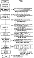
- Fig. 5 is a flowchart to illustrate the processing of an IF statement including list vector loading by a vector processing device of the present invention;
- Fig. 6 is a flowchart to illustrate the processing of an IF statement including list vector storing by a vector processing device of the present invention;
- Fig. 7 is an explanatory view to illustrate the operation caused by a vector compress instruction;
- Fig. 8 is an explanatory view to illustrate the operation caused by a vector expand instruction;
- Fig. 9 is a configuration example of a conventional vector processing device;
- Fig. 10 is a flowchart to illustrate a first conventional method of processing for an IF statement including list vector loading;
- Fig. 11 is a flowchart to illustrate a second conventional method of processing for an IF statement including list vector loading; and
- Fig. 12 is a flowchart to illustrate a conventional method of processing for an IF statement including list vector storing.
-
- Referring to the attached figures, preferred embodiments of the present invention will be described in detail below.
- Fig. 1 is a block diagram to show the configuration of a vector processing device according to a preferred embodiment of the present invention. A
vector processor 10 comprises more than one vector register (vector registers 12-1 to 12-8), avector control register 13, a plurality of operation devices (14-1 to 14-4) and acrossbar 15. The vector registers 12-1 to 12-8 and the vector control register 13 are connected to the operation devices 14-1 to 14-4 via thecrossbar 15. - The results obtained by the operation devices 14-1 to 14-4 can be stored to any of the vector registers 12-1 to 12-8. Further, in masked operation, mask data stored in the vector control register 13 controls whether or not to store the elements of the operation results to the vector registers 12-1 to 12-8. The vector registers 12-1 to 12-8 send data to and receive data from the
main storage 17 via the main storage controller 16 (to be described below). - The
main storage controller 16 comprises a mask registration means 18, an address information registration means 19, a load data storage means 21, a store data storage means 20 and a request generation means 25. The address information registration means 19 keeps the addresses to access themain storage 17 sent from the vector registers 12-1 to 12-8 and the store data storage means 20 keeps the vector data to be stored to themain storage 17. - The load data storage means 21 temporarily keeps the vector data obtained by accessing the
main storage 17. The mask registration means 18 keeps the mask data sent from thevector control register 13. Such mask data are sent to thevector processor 10 together with the load data stored in the load data storage means 21. The request generation means 25 converts the mask data stored in the mask registration means 18 into request signals. Themain storage 17 stores the store data in the store data storage means 20, only for the elements for which the request signals are received. - For processing of a masked list vector load instruction, the
main storage 17 is accessed at the addresses kept at the address information registration means 19. The data obtained by such accessing are temporarily stored in the load data storage means 21 and sent to thevector processor 10 together with the mask data in the mask registration means 18. For the elements of the vector register at the positions for which the mask data sent from themain storage controller 16 is "1", the load data sent from themain storage controller 16 are stored. For the vector register elements at the positions for which the mask data is "0", the load data sent from themain storage controller 16 are not stored and the data originally existing in the vector register are left. - For processing of a masked list vector store instruction, when the mask data stored in the mask registration means 18 is "1", the request generation means 25 converts such data into a request signal, which directs writing of data to the
main storage 17. When the mask data is "0", it does not convert the data into a request signal. Together with the data after conversion to a request signal, address and store data are sent to themain storage 17. Themain storage 17 stores the store data when it recognizes the request signal. In other words, the store data for the positions where the mask data in the mask registration means 18 is "1" are stored to themain storage 17, but those for the positions where the mask data is "0" are not stored to themain storage 17. - Fig. 2 shows the configuration of a vector processing device according to a second embodiment of the present invention. In the figure, a
vector processor 10 has the same configuration as the first embodiment shown in Fig. 1. - A
main storage controller 16 comprises a mask registration means 18, a memory access information registration means 24, a load data storage means 21, a memory access control means 22, a load data expansion means 23. The memory access information registration means 24 comprises an address information registration means 19 to store the addresses for access to themain storage 17 and a store data storage means 20 to store the data to be stored to themain storage 17. - The mask registration means 18 keeps the mask data sent from the vector control register 13 in the
vector processor 10 and the memory access control means 22 selects the information for access to themain storage 17 from the memory access information registration mean 24 according to the mask data contents stored in the mask registration means 18. - For processing of a list vector load instruction, the memory access control means 22 controls the device so that it accesses the
main storage 17 at the addresses, among those kept at the address information registration means 19, corresponding to the positions for which the mask data stored in the mask registration means 18 is "1" and does not access themain storage 17 at the addresses corresponding to the positions for which the mask data is "0". - The load data obtained by such access to the
main storage 17 are temporarily kept at the load data storage means 21. The load data expansion means 23 expands the load data in the load data storage means 21 according to the same principle as the VEX instruction. Specifically, it expands the load data for the positions where the mask data is "1" and stores an arbitrary value for the positions where the mask data is "0". - The values in the above step need not to be assured. When the data generated by the load data expansion means 23 are sent to the
vector processor 10 to be stored to an arbitrary vector register, the mask data at the mask registration means 18 are together sent to thevector processor 10. Thus, the data sent from themain storage 16 are stored for the vector register elements at the positions for which the mask data is "1". For the positions where the mask data is "0", the data originally stored in the vector register are left and the data sent from themain storage controller 16 are not stored. - Referring now to the data flow in Fig. 3, the operation for a masked list vector load instruction at the vector processing device according to the second embodiment is described.
- Suppose here that the vector register 12-1 keeps the address data A (a1, a2, a3 .... a10) for access to the
main storage 17, the vector register 12-2 keeps X (x1, x2, x3 ... , x10) and the vector control register 13 keeps the mask data (1, 1, 0, 1, 0, 1, 1, 0, 0, 1). - When a masked list vector load instruction is issued, the
vector processor 10 sends the address data and mask data to themain storage controller 16. The mask data (1, 1, 0, 1, 0, 1, 1, 0, 0, 1) are stored to the mask registration means 18 and the address data (a1, a2, a3, .... a10) are stored to the address information registration means 19. The memory access control means 22 sends the addresses for the positions where the mask data is "1" in the mask registration means 18, i.e. (a1, a2, a4, a6, a7, a10), to themain storage 17. Themain storage 17, upon receipt of these addresses, sends the data corresponding to these addresses (a1, a2, a4, a6, a7, a10) to the load data storage means 11. Suppose the data here are B(b1, b2, b4, b6, b7, b10). - The load data expansion means 23 stores the data B(b1, b2, b4, b6, b7, b10) to the positions where the mask data in the mask registration means 18 is "1" (first, second, fourth, sixth, seventh and tenth elements) and stores an arbitrary value (*) at the positions where the mask data is "0" (third, fifth, eighth and ninth elements). Thus, the data B'(b1, b2, *, b4, *, b6, b7, *, *, b10) are generated. Then the data B' are sent to the
vector processor 10 so as to be stored in the vector register 12-2. - When the data is stored to the vector register 12-2, the data B' elements are stored for the positions for which the mask data in the vector control register 13 is "1" (first, second, fourth, sixth, seventh and tenth elements). For the positions where the mask data is "0" (third, fifth, eighth and ninth elements), the data X elements (x3, x5, x8, x9) originally stored in the vector register 12-2 are kept. As a result, the vector register 12-2 has the vector data X'(b1, b2, x3, b4, x5, b6, b7, x8, x9, b10) after the masked list vector load instruction.
- For processing of a list vector store instruction, the store data elements in the store data storage means 20 corresponding to the positions for which the mask data in the mask registration means 18 is "1" are sent to the
main storage 17 together with the addresses corresponding to such elements in the address information registration means 19. Thus, the store data are stored to themain storage 17 with avoiding data replacement for the positions where the mask data is "0" in themain storage 17. - Referring now to the data flow in Fig. 4, the operation for a masked list vector store instruction at the vector processing device according to the second embodiment is described. Suppose here that the vector register 12-1 keeps the address data A (a1, a2, a3 .... a10) for access to the
main storage 17, the vector register 12-2 keeps B (b1, b2, b3 ... , b10) to be stored to themain storage 17 and the vector control register 13 keeps the mask data (1, 1, 0, 1, 0, 1, 1, 0, 0, 1). - When a masked list vector store instruction is issued, the
vector processor 10 sends the address data, store data and mask data to themain storage controller 16. The mask data (1, 1, 0, 1, 0, 1, 1, 0, 0, 1) are stored to the mask registration means 18, the address data (a1, a2, a3, .... a10) are stored to the address information registration means 19 and the data (b1, b2, b3, ... b10) are stored to the store data storage means 20. The memory access control means 22 sends the address and store data for the positions where the mask data is "1" in the mask registration means 18, i.e. (a1, a2, a4, a6, a7, a10) and (b1, b2, b4, b6, b7 and b10), to themain storage 17. Themain storage 17 stores the store data (b1, b2, b4, b6, b7, b10) to the positions specified by the addresses (a1, a2, a4, a6, a7, a10). - Referring to the flowchart and the register contents shown in Fig. 5, the vector processing device is now supposed to process, for example, the conditional expression (IF statement) as follows:
- DO 10 I = 1, N
- IF (M(I). EQ. 0)
- THEN
- X(I) = A(B(I)) + C(D(I))
- ELSE
- X(I) = 1
- 10 CONTINUE
-
- Firstly, a comparison instruction causes comparison of M(I) and 0. A subsequent mask generation instruction stores the mask data to the
vector control register 13. Suppose here that the mask data are (1, 1, 0, 1, 0, 1, 1, 0, ...). Then, the data B(I) and D(I) are loaded from themain storage 17 to the vector registers 12-1 and 12-2. - Next, a masked list vector load instruction causes the data in the vector registers 12-1 and 12-2 to be read out and sent to the
main storage controller 16, and at the same time causes the mask data in the vector control register 13 to be sent to themain storage controller 16. Themain storage controller 16 follows the method as described above to load the data A(B(I))(a1, a2, *, a4, *, a6, a7 ...) and (D(I))(c1, c2, *, c4, *, c6, c7,...) to the elements where the condition of the IF statement is true (first, second, fourth, sixth, seventh ... elements) and stores them to the vector registers 12-3 and 12-4. Then, the data in the vector registers 12-3 and 12-4 are read out and input to the adder 14-1 for processing, and the results are stored to the vector register 12-5. The vector register 12-5 is supposed to keep the vector data X(X1, X2, X3, X4, X5, X6, X7, ...) as the initial values. - Next, a mask reverse instruction reverses the bits in the vector control register 13 to obtain the data M'(0, 0, 1, 0, 1, 0, 0, 1). The elements in the vector register 12-5 for which the mask data is "1" (third, fifth, eighth .... elements) are replaced with the immediate value "1". Then, the contents of the vector register 12-5 are stored to the
main storage 17. - The IF statement processing as described above with the vector processing device according to the first or second embodiment reduces the number of accesses to the
main storage 17, and at the same time, shortens the data storing time for the vector registers. Further, such procedure using a masked list vector loading eliminates the need of conventional auxiliary operations, which improves the speed of processing. - Referring to the flowchart and the register contents in Fig. 6, another example of processing is described with supposing an IF statement as follows:
- DO 10 I = 1, N
- IF (M(I). EQ. 0) GO TO 10
- X(C(I)) = A(I)+B(I)
- 10 CONTINUE
-
- Firstly, a comparison instruction causes comparison of M(I) and 0. A subsequent mask generation instruction stores the mask data to the
vector control register 13. Suppose here that the mask data are (1, 1, 0, 1, 0, 1, 1, 0, ...). Then, the data A(I), B(I) and C(I) are loaded from themain storage 17 to the vector registers 12-1, 12-2 and 12-3. - Next, the data in the vector registers 12-1 and 12-2 are read out and input to the adder 14-1 for processing. The operation results are stored to the vector register 12-4, only for the elements at the positions where the mask data in the vector control register 13 is "1" (first, second, fourth, sixth, seventh .... elements). For the elements at the positions where the mask data is "0" (third, fifth, eighth .... elements), the initial data of the vector register 12-4 are left. The resulting data are (a1+b1, a2+b2, *, a4+b4, *, a6+b6, a7+b7, *, .... ). The vector register 12-5 is supposed to keep the vector data X(X1, X2, X3, X4, X5, X6, X7, ...) as the initial data.
- Next, a masked list vector store instruction reads out the address data and the store data from the vector registers 12-3 and 12-4 respectively and sends them to the
main storage controller 16. Themain storage controller 16, upon receipt of the address data and the store data, stores the store data to themain storage 17 only for the elements for which the condition in the IF statement is true (first, second, fourth, sixth, seventh ... elements). - With the vector processing device according to the first and the second embodiments, IF statements can be processed with a reduced number of accesses to the
main storage 17 and in a shorter time for data storing to the vector registers. Besides, masked list vector storing eliminates the need of conventional auxiliary operations, which improves the operation speed. - Thus, a masked list vector loading instruction during list vector loading for an IF statement eliminates the need of auxiliary operations. Since the load data can be obtained by access to the main storage only when the condition of the IF statement is true, such method further reduces the number of accesses to the main storage, which improves the speed of conditional list vector loading. In list vector storing for an IF statement, a masked vector store instruction eliminates the need of auxiliary operations. Besides, since the subject data are stored with access to the main storage only when the condition of the IF statement is true, the number of accesses to the main storage is reduced, which improves the speed of storing. This also eliminates the need of a compiler which changes the method of processing according to information including the rate of "true" for the applicable IF statement.
- Obviously, various modifications can be made to the above embodiments. It is intended to cover in the appended claims all such modifications and variations as fall within the true spirit and scope of the present invention.
Claims (4)
- A vector processing device comprising:a vector processor (10) further comprising more than one vector register (12-2,...,12-8), an operation means (14-1,...,14-4) for vector operations, and a vector control register (13) to store the mask information for the vector data,a vector data storage for storing said vector data, anda storage controller (16) for controlling accessing to said vector data storage based on a masked list vector instruction, said storage controller (16) further comprising an address data selection means (24) for selecting the address to access to said vector data storage stored at said vector register according to said mask information, and a data storing means for storing the vector data obtained by accessing to said vector data storage using said selected address to said vector register according to said mask information, wherein said address data selection means comprises an access information registration means (24) for storing the address for access to said vector data storage stored in said vector register,a mask registration means (18) for holding the mask information for said vector control register, and an access control means (22) for selecting the address from said address information registration means based on said mask information registered to said mask registration means,
said data storing means further comprisesa load data storage means (21) for temporarily storing the vector data obtained by access to said storage using the address data selected by said access control means, and a load data expansion means (23) for expanding the load vector data held at said load data storage means according to said mask information stored in said mask registration means and for storing the expanded load vector data to said vector register. - The vector processing device of Claim 1 wherein said address data selection means further comprises an access information registration means (24) having an address information registration means (19) to store the address data for access to said vector data storage stored in said vector register and a store data storage means (20) which keeps the vector data to be stored in said vector data storage, and an access control means (22) to obtain the store data to be stored in said vector data storage according to said mask information and the storing address on said vector data storage from said access information registration means (24).
- The vector processing device of Claim 1 or 2 wherein said access control means (22) accesses said vector data storage (17) at the addresses in said address information registration means (19) for which said mask information is '1", and does not access said vector data storage at the addresses of said address information registration means for which said mask information is "0".
- A vector processing device of Claim 1, 2, or 3 wherein said load data expansion means (23) stores said load data for the elements of said vector register for which said mask information is "1" and stores an arbitrary value for the elements of said vector register for which said mask information is "0".
Applications Claiming Priority (3)
| Application Number | Priority Date | Filing Date | Title |
|---|---|---|---|
| JP4158412A JP2665111B2 (en) | 1992-06-18 | 1992-06-18 | Vector processing equipment |
| JP15841292 | 1992-06-18 | ||
| EP93109683A EP0574909B1 (en) | 1992-06-18 | 1993-06-17 | Vector processing device |
Related Parent Applications (1)
| Application Number | Title | Priority Date | Filing Date |
|---|---|---|---|
| EP93109683A Division EP0574909B1 (en) | 1992-06-18 | 1993-06-17 | Vector processing device |
Publications (2)
| Publication Number | Publication Date |
|---|---|
| EP0926603A1 true EP0926603A1 (en) | 1999-06-30 |
| EP0926603B1 EP0926603B1 (en) | 2002-10-30 |
Family
ID=15671196
Family Applications (2)
| Application Number | Title | Priority Date | Filing Date |
|---|---|---|---|
| EP99101058A Expired - Lifetime EP0926603B1 (en) | 1992-06-18 | 1993-06-17 | Vector processing device |
| EP93109683A Expired - Lifetime EP0574909B1 (en) | 1992-06-18 | 1993-06-17 | Vector processing device |
Family Applications After (1)
| Application Number | Title | Priority Date | Filing Date |
|---|---|---|---|
| EP93109683A Expired - Lifetime EP0574909B1 (en) | 1992-06-18 | 1993-06-17 | Vector processing device |
Country Status (5)
| Country | Link |
|---|---|
| US (1) | US5511210A (en) |
| EP (2) | EP0926603B1 (en) |
| JP (1) | JP2665111B2 (en) |
| CA (1) | CA2098674C (en) |
| DE (2) | DE69329630T2 (en) |
Cited By (1)
| Publication number | Priority date | Publication date | Assignee | Title |
|---|---|---|---|---|
| US20090187739A1 (en) * | 1998-12-16 | 2009-07-23 | Mario Nemirovsky | Method and Apparatus for Improved Computer Load and Store Operations |
Families Citing this family (46)
| Publication number | Priority date | Publication date | Assignee | Title |
|---|---|---|---|---|
| JP3304444B2 (en) * | 1992-11-30 | 2002-07-22 | 富士通株式会社 | Vector processing equipment |
| US6006315A (en) * | 1996-10-18 | 1999-12-21 | Samsung Electronics Co., Ltd. | Computer methods for writing a scalar value to a vector |
| US6052769A (en) * | 1998-03-31 | 2000-04-18 | Intel Corporation | Method and apparatus for moving select non-contiguous bytes of packed data in a single instruction |
| US7020879B1 (en) | 1998-12-16 | 2006-03-28 | Mips Technologies, Inc. | Interrupt and exception handling for multi-streaming digital processors |
| US7257814B1 (en) | 1998-12-16 | 2007-08-14 | Mips Technologies, Inc. | Method and apparatus for implementing atomicity of memory operations in dynamic multi-streaming processors |
| US7237093B1 (en) | 1998-12-16 | 2007-06-26 | Mips Technologies, Inc. | Instruction fetching system in a multithreaded processor utilizing cache miss predictions to fetch instructions from multiple hardware streams |
| US6389449B1 (en) * | 1998-12-16 | 2002-05-14 | Clearwater Networks, Inc. | Interstream control and communications for multi-streaming digital processors |
| US7035997B1 (en) | 1998-12-16 | 2006-04-25 | Mips Technologies, Inc. | Methods and apparatus for improving fetching and dispatch of instructions in multithreaded processors |
| ATE440321T1 (en) * | 2000-01-18 | 2009-09-15 | Mips Tech Inc | METHOD AND APPARATUS FOR IMPROVED COMPUTER LOADING AND STORAGE OPERATIONS |
| JP2004518183A (en) | 2000-07-14 | 2004-06-17 | クリアウオーター・ネツトワークス・インコーポレイテツド | Instruction fetch and dispatch in multithreaded systems |
| US20020112145A1 (en) * | 2001-02-14 | 2002-08-15 | Bigbee Bryant E. | Method and apparatus for providing software compatibility in a processor architecture |
| US20100274988A1 (en) * | 2002-02-04 | 2010-10-28 | Mimar Tibet | Flexible vector modes of operation for SIMD processor |
| US7793084B1 (en) | 2002-07-22 | 2010-09-07 | Mimar Tibet | Efficient handling of vector high-level language conditional constructs in a SIMD processor |
| US6741257B1 (en) | 2003-01-20 | 2004-05-25 | Neomagic Corp. | Graphics engine command FIFO for programming multiple registers using a mapping index with register offsets |
| US7873812B1 (en) | 2004-04-05 | 2011-01-18 | Tibet MIMAR | Method and system for efficient matrix multiplication in a SIMD processor architecture |
| US7725678B2 (en) * | 2005-02-17 | 2010-05-25 | Texas Instruments Incorporated | Method and apparatus for producing an index vector for use in performing a vector permute operation |
| US7765386B2 (en) * | 2005-09-28 | 2010-07-27 | Intel Corporation | Scalable parallel pipeline floating-point unit for vector processing |
| US7404065B2 (en) * | 2005-12-21 | 2008-07-22 | Intel Corporation | Flow optimization and prediction for VSSE memory operations |
| US7600104B2 (en) * | 2006-08-15 | 2009-10-06 | Peter Neumann | Method and system for parallel vector data processing of vector data having a number of data elements including a defined first bit-length |
| US9069547B2 (en) * | 2006-09-22 | 2015-06-30 | Intel Corporation | Instruction and logic for processing text strings |
| US20090172348A1 (en) * | 2007-12-26 | 2009-07-02 | Robert Cavin | Methods, apparatus, and instructions for processing vector data |
| US9529592B2 (en) | 2007-12-27 | 2016-12-27 | Intel Corporation | Vector mask memory access instructions to perform individual and sequential memory access operations if an exception occurs during a full width memory access operation |
| US8909901B2 (en) | 2007-12-28 | 2014-12-09 | Intel Corporation | Permute operations with flexible zero control |
| US10387151B2 (en) * | 2007-12-31 | 2019-08-20 | Intel Corporation | Processor and method for tracking progress of gathering/scattering data element pairs in different cache memory banks |
| US7984273B2 (en) | 2007-12-31 | 2011-07-19 | Intel Corporation | System and method for using a mask register to track progress of gathering elements from memory |
| GB2470782B (en) | 2009-06-05 | 2014-10-22 | Advanced Risc Mach Ltd | A data processing apparatus and method for handling vector instructions |
| US10175990B2 (en) | 2009-12-22 | 2019-01-08 | Intel Corporation | Gathering and scattering multiple data elements |
| US8271433B2 (en) * | 2009-12-30 | 2012-09-18 | Nokia Corporation | Method and apparatus for providing automatic controlled value expansion of information |
| US20120254592A1 (en) * | 2011-04-01 | 2012-10-04 | Jesus Corbal San Adrian | Systems, apparatuses, and methods for expanding a memory source into a destination register and compressing a source register into a destination memory location |
| WO2013048368A1 (en) * | 2011-09-26 | 2013-04-04 | Intel Corporation | Instruction and logic to provide vector scatter-op and gather-op functionality |
| DE112011105666T5 (en) * | 2011-09-26 | 2014-07-10 | Intel Corp. | Command and logic for providing vector loading OP / memory OP with step functionality |
| GB2507018B (en) * | 2011-09-26 | 2020-04-22 | Intel Corp | Instruction and logic to provide vector loads and stores with strides and masking functionality |
| WO2013095653A1 (en) * | 2011-12-23 | 2013-06-27 | Intel Corporation | Systems, apparatuses, and methods for performing a conversion of a writemask register to a list of index values in a vector register |
| US9400650B2 (en) * | 2012-09-28 | 2016-07-26 | Intel Corporation | Read and write masks update instruction for vectorization of recursive computations over interdependent data |
| US9378182B2 (en) * | 2012-09-28 | 2016-06-28 | Intel Corporation | Vector move instruction controlled by read and write masks |
| US9606961B2 (en) | 2012-10-30 | 2017-03-28 | Intel Corporation | Instruction and logic to provide vector compress and rotate functionality |
| US9501276B2 (en) * | 2012-12-31 | 2016-11-22 | Intel Corporation | Instructions and logic to vectorize conditional loops |
| US9244684B2 (en) | 2013-03-15 | 2016-01-26 | Intel Corporation | Limited range vector memory access instructions, processors, methods, and systems |
| US9645820B2 (en) | 2013-06-27 | 2017-05-09 | Intel Corporation | Apparatus and method to reserve and permute bits in a mask register |
| US10503502B2 (en) * | 2015-09-25 | 2019-12-10 | Intel Corporation | Data element rearrangement, processors, methods, systems, and instructions |
| JP2018124877A (en) * | 2017-02-02 | 2018-08-09 | 富士通株式会社 | Code generating device, code generating method, and code generating program |
| US11340904B2 (en) * | 2019-05-20 | 2022-05-24 | Micron Technology, Inc. | Vector index registers |
| US11403256B2 (en) | 2019-05-20 | 2022-08-02 | Micron Technology, Inc. | Conditional operations in a vector processor having true and false vector index registers |
| US11507374B2 (en) * | 2019-05-20 | 2022-11-22 | Micron Technology, Inc. | True/false vector index registers and methods of populating thereof |
| US11327862B2 (en) | 2019-05-20 | 2022-05-10 | Micron Technology, Inc. | Multi-lane solutions for addressing vector elements using vector index registers |
| CN115934449B (en) * | 2023-02-08 | 2023-06-02 | 合肥智芯半导体有限公司 | Register verification method, device and equipment |
Citations (2)
| Publication number | Priority date | Publication date | Assignee | Title |
|---|---|---|---|---|
| US4621324A (en) * | 1982-12-17 | 1986-11-04 | Hitachi, Ltd. | Processor for carrying out vector operation wherein the same vector element is used repeatedly in succession |
| EP0240032A2 (en) * | 1986-04-04 | 1987-10-07 | Hitachi, Ltd. | Vector processor with vector data compression/expansion capability |
Family Cites Families (9)
| Publication number | Priority date | Publication date | Assignee | Title |
|---|---|---|---|---|
| JPS57209570A (en) * | 1981-06-19 | 1982-12-22 | Fujitsu Ltd | Vector processing device |
| JPS6015771A (en) * | 1983-07-08 | 1985-01-26 | Hitachi Ltd | Memory controller |
| JPS6069746A (en) * | 1983-09-26 | 1985-04-20 | Fujitsu Ltd | Control system of vector data processor |
| US4791555A (en) * | 1983-10-24 | 1988-12-13 | International Business Machines Corporation | Vector processing unit |
| JPS62276668A (en) * | 1985-07-31 | 1987-12-01 | Nec Corp | Vector mask operation control unit |
| US4740893A (en) * | 1985-08-07 | 1988-04-26 | International Business Machines Corp. | Method for reducing the time for switching between programs |
| JPS6266377A (en) * | 1985-09-19 | 1987-03-25 | Fujitsu Ltd | Mask pattern generation system |
| JPS63251835A (en) * | 1987-04-08 | 1988-10-19 | Hitachi Ltd | Vector processor |
| JP2607689B2 (en) * | 1989-07-10 | 1997-05-07 | 株式会社日立製作所 | Vector processing equipment |
-
1992
- 1992-06-18 JP JP4158412A patent/JP2665111B2/en not_active Expired - Fee Related
-
1993
- 1993-06-17 CA CA002098674A patent/CA2098674C/en not_active Expired - Fee Related
- 1993-06-17 DE DE69329630T patent/DE69329630T2/en not_active Expired - Fee Related
- 1993-06-17 DE DE69332458T patent/DE69332458T2/en not_active Expired - Fee Related
- 1993-06-17 EP EP99101058A patent/EP0926603B1/en not_active Expired - Lifetime
- 1993-06-17 EP EP93109683A patent/EP0574909B1/en not_active Expired - Lifetime
- 1993-06-18 US US08/077,739 patent/US5511210A/en not_active Expired - Fee Related
Patent Citations (2)
| Publication number | Priority date | Publication date | Assignee | Title |
|---|---|---|---|---|
| US4621324A (en) * | 1982-12-17 | 1986-11-04 | Hitachi, Ltd. | Processor for carrying out vector operation wherein the same vector element is used repeatedly in succession |
| EP0240032A2 (en) * | 1986-04-04 | 1987-10-07 | Hitachi, Ltd. | Vector processor with vector data compression/expansion capability |
Cited By (1)
| Publication number | Priority date | Publication date | Assignee | Title |
|---|---|---|---|---|
| US20090187739A1 (en) * | 1998-12-16 | 2009-07-23 | Mario Nemirovsky | Method and Apparatus for Improved Computer Load and Store Operations |
Also Published As
| Publication number | Publication date |
|---|---|
| EP0574909A2 (en) | 1993-12-22 |
| EP0574909A3 (en) | 1995-05-10 |
| DE69329630T2 (en) | 2001-03-01 |
| DE69332458T2 (en) | 2003-03-20 |
| EP0574909B1 (en) | 2000-11-08 |
| US5511210A (en) | 1996-04-23 |
| CA2098674C (en) | 1999-03-02 |
| CA2098674A1 (en) | 1993-12-19 |
| JP2665111B2 (en) | 1997-10-22 |
| DE69329630D1 (en) | 2000-12-14 |
| DE69332458D1 (en) | 2002-12-05 |
| EP0926603B1 (en) | 2002-10-30 |
| JPH0644292A (en) | 1994-02-18 |
Similar Documents
| Publication | Publication Date | Title |
|---|---|---|
| US5511210A (en) | Vector processing device using address data and mask information to generate signal that indicates which addresses are to be accessed from the main memory | |
| US6275749B1 (en) | Interrupt-controlled thread processing | |
| US20010032296A1 (en) | Data processor | |
| US5594878A (en) | Bus interface structure and system for controlling the bus interface structure | |
| EP0389175A3 (en) | Data prefetch system | |
| US4646230A (en) | Data transfer control system | |
| CN109727187B (en) | Method and device for adjusting storage position of multiple region of interest data | |
| EP0734139A2 (en) | A data transfer device with cluster control | |
| US6134640A (en) | Method for transforming flash memory storage format based on average data length | |
| US4975835A (en) | Variable length data processing apparatus for consecutively processing variable-length data responsive to one instruction | |
| EP0240606A2 (en) | Pipe-line processing system and microprocessor using the system | |
| EP0260837B1 (en) | Microprocessor with selective cache memory | |
| US6518973B1 (en) | Method, system, and computer program product for efficient buffer level management of memory-buffered graphics data | |
| US5604842A (en) | Fuzzy reasoning processor and method, and rule setting apparatus and method | |
| EP0426111A2 (en) | Memory control system | |
| US5428801A (en) | Data array conversion control system for controlling conversion of data arrays being transferred between two processing systems | |
| EP0230536A1 (en) | I/O processor for programmable sequence controller | |
| EP0811922A1 (en) | Peripheral device control | |
| CA2157435C (en) | Vector data bypass mechanism for vector computer | |
| US5500830A (en) | Memory access device | |
| KR100654477B1 (en) | Object oriented processing with dedicated pointer memories | |
| US7200739B2 (en) | Generation of modified command sequence from original command by feeding back for subsequent modification based on decode control signal | |
| KR100188027B1 (en) | Address generation circuit | |
| JPH1040165A (en) | Data read method and read buffer | |
| US5524221A (en) | Next instruction pointer calculation system for a microcomputer |
Legal Events
| Date | Code | Title | Description |
|---|---|---|---|
| PUAI | Public reference made under article 153(3) epc to a published international application that has entered the european phase |
Free format text: ORIGINAL CODE: 0009012 |
|
| AC | Divisional application: reference to earlier application |
Ref document number: 574909 Country of ref document: EP |
|
| AK | Designated contracting states |
Kind code of ref document: A1 Designated state(s): DE FR NL |
|
| 17P | Request for examination filed |
Effective date: 19990512 |
|
| 17Q | First examination report despatched |
Effective date: 20000412 |
|
| RIC1 | Information provided on ipc code assigned before grant |
Free format text: 7G 06F 15/78 A, 7G 06F 17/16 B |
|
| GRAG | Despatch of communication of intention to grant |
Free format text: ORIGINAL CODE: EPIDOS AGRA |
|
| GRAG | Despatch of communication of intention to grant |
Free format text: ORIGINAL CODE: EPIDOS AGRA |
|
| GRAG | Despatch of communication of intention to grant |
Free format text: ORIGINAL CODE: EPIDOS AGRA |
|
| GRAH | Despatch of communication of intention to grant a patent |
Free format text: ORIGINAL CODE: EPIDOS IGRA |
|
| GRAH | Despatch of communication of intention to grant a patent |
Free format text: ORIGINAL CODE: EPIDOS IGRA |
|
| GRAA | (expected) grant |
Free format text: ORIGINAL CODE: 0009210 |
|
| AC | Divisional application: reference to earlier application |
Ref document number: 574909 Country of ref document: EP |
|
| AK | Designated contracting states |
Kind code of ref document: B1 Designated state(s): DE FR NL |
|
| REF | Corresponds to: |
Ref document number: 69332458 Country of ref document: DE Date of ref document: 20021205 |
|
| ET | Fr: translation filed | ||
| PLBE | No opposition filed within time limit |
Free format text: ORIGINAL CODE: 0009261 |
|
| STAA | Information on the status of an ep patent application or granted ep patent |
Free format text: STATUS: NO OPPOSITION FILED WITHIN TIME LIMIT |
|
| 26N | No opposition filed |
Effective date: 20030731 |
|
| PGFP | Annual fee paid to national office [announced via postgrant information from national office to epo] |
Ref country code: DE Payment date: 20070614 Year of fee payment: 15 |
|
| PGFP | Annual fee paid to national office [announced via postgrant information from national office to epo] |
Ref country code: NL Payment date: 20070617 Year of fee payment: 15 |
|
| PGFP | Annual fee paid to national office [announced via postgrant information from national office to epo] |
Ref country code: FR Payment date: 20070608 Year of fee payment: 15 |
|
| NLV4 | Nl: lapsed or anulled due to non-payment of the annual fee |
Effective date: 20090101 |
|
| REG | Reference to a national code |
Ref country code: FR Ref legal event code: ST Effective date: 20090228 |
|
| PG25 | Lapsed in a contracting state [announced via postgrant information from national office to epo] |
Ref country code: DE Free format text: LAPSE BECAUSE OF NON-PAYMENT OF DUE FEES Effective date: 20090101 |
|
| PG25 | Lapsed in a contracting state [announced via postgrant information from national office to epo] |
Ref country code: NL Free format text: LAPSE BECAUSE OF NON-PAYMENT OF DUE FEES Effective date: 20090101 |
|
| PG25 | Lapsed in a contracting state [announced via postgrant information from national office to epo] |
Ref country code: FR Free format text: LAPSE BECAUSE OF NON-PAYMENT OF DUE FEES Effective date: 20080630 |