EP0186044A2 - Photodétecteur - Google Patents
Photodétecteur Download PDFInfo
- Publication number
- EP0186044A2 EP0186044A2 EP85115750A EP85115750A EP0186044A2 EP 0186044 A2 EP0186044 A2 EP 0186044A2 EP 85115750 A EP85115750 A EP 85115750A EP 85115750 A EP85115750 A EP 85115750A EP 0186044 A2 EP0186044 A2 EP 0186044A2
- Authority
- EP
- European Patent Office
- Prior art keywords
- light receiving
- photocell
- receiving surface
- photodetector
- light
- Prior art date
- Legal status (The legal status is an assumption and is not a legal conclusion. Google has not performed a legal analysis and makes no representation as to the accuracy of the status listed.)
- Granted
Links
- 229920005989 resin Polymers 0.000 claims abstract description 41
- 239000011347 resin Substances 0.000 claims abstract description 41
- 239000000758 substrate Substances 0.000 claims abstract description 12
- 239000011248 coating agent Substances 0.000 claims description 8
- 238000000576 coating method Methods 0.000 claims description 8
- 238000007373 indentation Methods 0.000 claims description 4
- 239000011247 coating layer Substances 0.000 claims 1
- 239000010410 layer Substances 0.000 claims 1
- 230000003287 optical effect Effects 0.000 description 15
- 238000000034 method Methods 0.000 description 6
- 230000001419 dependent effect Effects 0.000 description 5
- 238000010586 diagram Methods 0.000 description 5
- 239000000463 material Substances 0.000 description 3
- 238000005488 sandblasting Methods 0.000 description 3
- 238000004381 surface treatment Methods 0.000 description 3
- 241000220450 Cajanus cajan Species 0.000 description 2
- 230000015572 biosynthetic process Effects 0.000 description 2
- 239000003822 epoxy resin Substances 0.000 description 2
- 230000001747 exhibiting effect Effects 0.000 description 2
- 238000012986 modification Methods 0.000 description 2
- 230000004048 modification Effects 0.000 description 2
- 229920000647 polyepoxide Polymers 0.000 description 2
- 239000000126 substance Substances 0.000 description 2
- 229920003002 synthetic resin Polymers 0.000 description 2
- 239000000057 synthetic resin Substances 0.000 description 2
- 201000009310 astigmatism Diseases 0.000 description 1
- 230000006866 deterioration Effects 0.000 description 1
- 230000001627 detrimental effect Effects 0.000 description 1
- 238000006073 displacement reaction Methods 0.000 description 1
- 230000000694 effects Effects 0.000 description 1
- 238000002474 experimental method Methods 0.000 description 1
- 238000010438 heat treatment Methods 0.000 description 1
- 238000007689 inspection Methods 0.000 description 1
- 238000000465 moulding Methods 0.000 description 1
- 238000010422 painting Methods 0.000 description 1
- 238000007788 roughening Methods 0.000 description 1
- 239000004065 semiconductor Substances 0.000 description 1
- 238000005507 spraying Methods 0.000 description 1
- 230000008961 swelling Effects 0.000 description 1
Images


Classifications
-
- H01L31/0203—
-
- G—PHYSICS
- G11—INFORMATION STORAGE
- G11B—INFORMATION STORAGE BASED ON RELATIVE MOVEMENT BETWEEN RECORD CARRIER AND TRANSDUCER
- G11B7/00—Recording or reproducing by optical means, e.g. recording using a thermal beam of optical radiation by modifying optical properties or the physical structure, reproducing using an optical beam at lower power by sensing optical properties; Record carriers therefor
- G11B7/08—Disposition or mounting of heads or light sources relatively to record carriers
- G11B7/09—Disposition or mounting of heads or light sources relatively to record carriers with provision for moving the light beam or focus plane for the purpose of maintaining alignment of the light beam relative to the record carrier during transducing operation, e.g. to compensate for surface irregularities of the latter or for track following
-
- G—PHYSICS
- G11—INFORMATION STORAGE
- G11B—INFORMATION STORAGE BASED ON RELATIVE MOVEMENT BETWEEN RECORD CARRIER AND TRANSDUCER
- G11B7/00—Recording or reproducing by optical means, e.g. recording using a thermal beam of optical radiation by modifying optical properties or the physical structure, reproducing using an optical beam at lower power by sensing optical properties; Record carriers therefor
- G11B7/12—Heads, e.g. forming of the optical beam spot or modulation of the optical beam
- G11B7/13—Optical detectors therefor
-
- H—ELECTRICITY
- H01—ELECTRIC ELEMENTS
- H01L—SEMICONDUCTOR DEVICES NOT COVERED BY CLASS H10
- H01L25/00—Assemblies consisting of a plurality of semiconductor or other solid state devices
- H01L25/03—Assemblies consisting of a plurality of semiconductor or other solid state devices all the devices being of a type provided for in a single subclass of subclasses H10B, H10F, H10H, H10K or H10N, e.g. assemblies of rectifier diodes
- H01L25/04—Assemblies consisting of a plurality of semiconductor or other solid state devices all the devices being of a type provided for in a single subclass of subclasses H10B, H10F, H10H, H10K or H10N, e.g. assemblies of rectifier diodes the devices not having separate containers
- H01L25/041—Assemblies consisting of a plurality of semiconductor or other solid state devices all the devices being of a type provided for in a single subclass of subclasses H10B, H10F, H10H, H10K or H10N, e.g. assemblies of rectifier diodes the devices not having separate containers the devices being of a type provided for in subclass H10F
- H01L25/042—Assemblies consisting of a plurality of semiconductor or other solid state devices all the devices being of a type provided for in a single subclass of subclasses H10B, H10F, H10H, H10K or H10N, e.g. assemblies of rectifier diodes the devices not having separate containers the devices being of a type provided for in subclass H10F the devices being arranged next to each other
-
- H01L31/02325—
Definitions
- the present invention generally relates to a photodetector and, more particularly, to the photodetector suited for use as an optical pick-up head for optically recording or reproducing information on or from an optical information carrier medium.
- optical video disc system is nowadays well-known wherein information recorded on an optical information carrier medium, for example, a video disc, is optoelec- trically reproduced.
- the optical video disc system makes use of am,optical pick-up head and a laser as a source of light to be eventually detected by the pick-up head.
- Fig. 7 of the accompanying drawings illustrates a popular example of optical pick-up head system, wherein reference numerals 1, 2, 3, 4, 5, 6, 7 and 8 represent a semiconductor laser, a diffraction grating, a beam splitting prism, an objective lens assembly, a concave lens, a cylindrical lens, a photodetector, and a video disc, respectively.
- a tracking control system used therein is a three-beam tracking control system, wherein a tracking error signal can be detected by a pair of photocells 7a and 7b for tracking purpose formed in the photodetector 7.
- a focus control system is an astigmatism system, wherein a focusing error signal can be detected by a four-segment photocell 7c.
- An information (RF) signal can be detected by the four-segment photocell 7c.
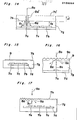
- the photodetector 7 is of a type formed by molding a synthetic resin, for example, transparent epoxy resin, the structure of which is shown in Figs. 8 and 9.
- the photodetector 7 comprises a substrate 7d on which the photocells 7a, 7b and 7c are formed, lead wires 7e for feeding respective outputs from the photocells, and output terminal members 7f for connecting the photocells with external circuit wirings, all of said substrate 7d, the lead wires 7e and portions of the terminal members 7f being embedded in a molded transparent resin layer 7g.
- Built-in functional units are arranged at a substantially central portion of the molded resin with respective light receiving faces 7a', 7b' and 7c' of the photocells held parallel to a light receiving surface 7h of the resin layer 7g.
- Outputs ' (currents) from the associated photocells 7a and 7b for tracking purpose are converted into respective voltages by a tracking signal processing circuitry shown in Fig. 10.
- 11(b) illustrates the waveform of the tracking error signal.
- an intermediate point (1/2 of the value P-P) of the TE signal does not coincide with the GND level because of conditions of an optical system as well as the difference in DC level of the outputs Sa and Sb and also in output level, and for compensating for a deviation of the intermediate point by means of a circuit, either the resistance R4 or R1 or the resistance R6 or R3 is adjusted to bring the intermediate point into coincidence with the GND level.
- a tracking servo since a tracking servo is apt to function to_bring the intermediate point into coincidence with the GND level in the event of deviation occurring between the intermediate point and the GND level, it will have an offset in a tracking direction when the deviation exceeds a predetermined quantity, and in this case the servo will no longer function.
- Fig. 12 illustrates a temperature-dependent change of the tracking error signal, and as shown therein, the tracking error signal TE once adjusted at normal temperature undergoes a change with change in temperature T and, at a certain temperature, displaces to a position shown by TE'.
- Fig. 13 illustrates the temperature dependent characteristic of the rate of change a in the conventional optical pick-up head, and it has been found that the change rate a often attains 15 to 20% at maximum and, moreover, the change rate a varies in swelling fashion at a predetermined interval of temperature, for example, by the effect of a temperature difference of 10 to 15°C.
- the change rate a attains a peak value at a temperature 10 to 15°C higher than the normal temperature. Accordingly, at a temperature as high as the temperature at which the change rate a exceeds 10%, the tracking operation tends to become unstable.
- Fig. 14 is a diagram used to explain how the light interference occurs as a result of difference in optical path, and a beam BO of light for tracking purpose enters the light receiving surface 7h of the molded resin layer and is subsequently detected by the photocell 7a.
- the position of the light receiving surface. of the molded resin layer is located at a level 7h at the time the position and the intensity of the incident beam have been initially adjusted at normal temperature, and when the temperature has increased to a value higher than the normal temperature by a predetermined value, the molded resin layer undergoes a thermal expansion with the light receiving surface consequently shifted to a position shown by 7h'.
- the distance between the light receiving face of the photocell 7a and the light receiving surface 7h is expressed by l1
- the distance between the light receiving surfaces 7h and 7h' is expressed by ⁇ l.
- the incident beam BO after having impinged upon the light receiving face of the photocell 7a is partially reflected therefrom towards the light receiving surface of the molded resin layer as shown by B2 or B2', and when and after the distance ⁇ l has attained a value which brings about the interference of light, the reflected light interferes with the incoming incident beam BO producing a pattern of dark and bright fringes on the light receiving face of the photocell 7a.
- the interference occurs when the relationship expressed by the following equation is satisfied: wherein n is a positive integer other than 0.
- n is a positive integer other than 0.
- the interference of bright fringes and that of dark fringes occurs, respectively.
- the interference of the dark and bright fringes alternating at intervals of a quarter wavelength is produced with the consequence that the photocell 7a generates a DC current of varying level.
- the rate of change a attributable to the varying level of the DC current produced from the photocell 7a will vary.
- the bright fringes and the dark fringes are produced at respective temperatures Tl and T2
- the change in temperature from the value T1 to the value T2 results in the change in the value ⁇ l in a quantity corresponding to one fourth of the wavelength ⁇ as can be understood from equation (1).
- the graph of Fig. 13 applies where the thickness of the resin molded layer having a coefficient of thermal expansion which is 5.2 x 10 -5 °C is 600 ⁇ m and the wavelength ⁇ of the laser beam is 800 nm.
- Japanese Laid-open Utility Model Publication No. 56-157762 laid open to public inspection in 1981, has proposed to use a light reflecting film on the surface of the resin molded product.
- a complete bond between the film and the resin surface cannot be achieved without difficulty and, also, the heat treatment used to form the film often results in the deterioration (for example, reduction in light transmissivity) of the resin molded body.
- the present invention has been developed with a view to substantially eliminating the above described disadvantages and inconveniences and has for its essential object to provide an improved photodetector wherein means is incorporated to minimize the temperature-dependent change of the tracking error signal.
- This and other objects of the present invention can be accomplished by providing the resin molded body having a light receiving surface inclined at a predetermined angle relative to the light receiving face of at least one photocell embedded in the resin molded body.
- the light receiving surface of the resin molded body is finely roughened to have a multiplicity of alternating hills and dales parallel to each other. According to a further embodiment of the present invention, however, a portion of the light receiving surface of the resin molded body which is in register with the photocell embedded therein is offset in level from the plane in which the remaining portion of the light receiving surface lies, i.e., either concaved or convexed.
- the secondary reflected light can be scattered and, therefore, the amount of light reflected back towards the light receiving face of the photocell can be minimized, with the consequent minimization of the above described interference of -light.
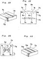
- a photodetector 7 shown therein comprises a photocell assembly including a substrate 7d with photocells 7a, 7b and 7c formed on one surface of the substrate 7d, the photocell assembly being completely embedded in a transparent resin molded body 7g of generally cubical configuration.
- the photocells 7a to 7c have their respective light receiving faces or "windows" 7a', 7b' and 7c' all lying in the same plane, whereas the resin molded body 7g has a light receiving surface 7i so defined and so located as to permit the incoming beam BO of light to travel direct to the windows 7a' to 7c' of the respective photocells 7a to 7c through such light receiving surface 7i.
- the light receiving surface 7i is planar and lies in parallel relation to the plane occupied by the photocell windows 7a' to 7c' as hereinbefore discussed with reference to Figs. 8 and 9.
- the light receiving surface 7i is planar, but is inclined at a predetermined angle 9 relative to the plane occupied by the photocell windows 7a' to 7c', said angle 0 being selected to be within the range of 1.5 to 6 degrees.
- the plane occupied by the photocell windows 7a' to 7c' assumes the right-angled relationship with the direction of travel of the incoming light B0 when and so long as the photodetector 7 is in use.
- the angle 9 of inclination is smaller than the minimal limit of 1.5°, the amount of light reflected from the light receiving surface 7i towards the photocell windows 7a' to 7c' after having been reflected by the photocell windows 7a' to 7c', that is, the amount of the secondary reflected light B2, will be great and no interference of light discussed hereinbefore can be minimized so much as expected.
- the inclination angle ⁇ is greater than the maximum limit of 6°, the incoming light BO will be reflected and/or diffracted in an increased quantity to such an extent as to result_in the reduced intensity of light falling on the photocell windows 7a' to 7c'.
- the embodiment of the present invention shown in Fig. 3 is such that the photocell assembly is embedded in the resin molded body 7g in an inclined fashion so that the plane occupied by the photocell windows 7a' to 7c' can converge with the light receiving surface 7i at the predetermined angle 9.
- the light receiving surface of the resin molded body 7g is so recessed as to provide an intermediate surface area 7j parallel to the photocell window 7c', and a pair of side surface areas 7k and 71 defined on respective sides of the surface area 7j in register with the associated photocell windows 7a' and 7b' and inclined upwardly therefrom in respective directions away from each other so as to converge at a predetermined angle 01 with a plane parallel to any one of the surface area 7j and the photocell windows 7a' to 7c'.
- the light receiving surface of the resin molded body 7g may be raised outwardly.
- Fig. 5 illustrates that when the photodetector constructed as hereinbefore described according to the present invention was used for detecting the tracking error, the rate of change of the photodetector of the present invention has been suppressed to a maximum value of 6 to 7% as shown by the solid line, in contrast to the maximum value of 15 to 20% exhibited by the prior art photodetector as shown by the broken line.
- Fig. 6 illustrates the rates of change exhibited by samples of photodetectors according to the present invention (shown by small circles) and those according to the prior art (shown by x), and it is clear that the rate of change exhibited by the photodetector according to the present invention is lower than that according to the prior art. All of these results are the outcome of the minimized interference of light as hereinbefore discussed.
- the light receiving surface of the resin molded body 7g is covered by a transparent coating 9 for scattering rays of light reflected by the photocell windows 7a' to 7c' as indicated by B2 in Fig. 16, thereby to minimize the secodnary reflected light.
- a material for the transparent coating 9 is preferred to be a moldable transparent resin of the same quality as the material for the resin molded body 7g or of a quality capable of exhibiting excellent adhesion or bond with the resin body 7g.
- the material for the coating 9 include, for example, an epoxy resin, a UV curable synthetic resin and others.
- the coating 9 should be as thin as possible, preferably not greater than 100 ⁇ m in thickness.
- the coating 9 may be formed by the use of any suitable method, provided that such method is effective to render one of the opposite surfaces of the coating 9 remote from the resin molded body 7g to be roughened as shown by 9a in Fig. 16. Such method may include, for example, a spray coating method or a painting. method which is to be practiced while the photodetector is oscillated.
- the light receiving surface 7h of the resin molded body is roughened so as to have a plurality of alternating hills and dales extending parallel to each other. This can be readily accomplished by the use of a mold assembly having a portion of the mold cavity so patterned as to produce the roughened light receiving surface 7h.
- the surface roughening can also be achieved by providing the light receiving surface 7h with a plurality of fine projections 7i as shown in Figs. 18 and 19, or a plurality of fine recesses.
- the formation of the fine projections 7i or the fine recesses may be carried out by the use of a sand blasting technique, in which case the sand blasting is preferably followed by a surface treatment such as, for example, an electropolishing or a chemical surface treatment because the sand blasting process lowers the light transmissivity of the light receiving surface 7h.
- a surface treatment such as, for example, an electropolishing or a chemical surface treatment because the sand blasting process lowers the light transmissivity of the light receiving surface 7h.
- the electropolishing or the chemical surface treatment it should be practiced to such an extent as to leave surface indentations on the light receiving surface 7h.
- the photodetector according to any one of the embodiments shown in and described with reference to Figs. 15 to 19 has been found exhibiting the same characteristic as shown in and described with reference to Fig. 5.
- the light receiving surface 7h is formed with a spherical recess 7m, 50 to 100 pm in depth and 500 to 800 pm in diameter, the diameter being enough to cover all of the photocell windows 7a' to 7c' as best shown in Fig. 21.
- a spherical projection 50 to 100 ⁇ m in height and 500 to 800 ⁇ m in diameter, may be formed on the light receiving surface 7h.
- spherical recesses 7o are formed on the light receiving surface 7h in register with the photocell windows 7a' and 7b' is shown in Figs. 23 and 24.
- spherical projections may be employed in place of the spherical recesses 7 0 .
- each of the spherical recesses 7o or the spherical projections is preferred to have a depth or height within the range of 50 to 100 pm and a diameter within the range of 150 to 170 ⁇ m.
- the or each spherical recess or the height of the or each spherical projection will undesirably act as a lens obstructing the formation of a beam spot of effective size on all of the photocell windows or the associated photocell window.
- a straight groove 7n is formed in the light receiving surface 7h of the resin molded body 7g.
- the direction in which the groove 7n extends may be either a direction shown by x in Fig. 21 or a direction shown by y in Fig. 21.
- a ridge or elongated projection may be formed on the light receiving surface 7h.
- two parallel straight grooves 7na and 7nb, or two parallel ridges or elongated projections may be formed on the light receiving surface 7h so as to extend in a direction shown by x in Fig. 24, as shown in Fig. 25.
- the depth or height of the or each groove or ridge is preferred to be within the range of 50 to 100 ⁇ m by the reason discussed in connection with the embodiments of Figs. 20 and 23.
- the width of the groove or ridge it is preferred to be within the range of 500 to 800 ⁇ m where the number thereof is one such as shown in Fig. 22, or within the range of 150 to 170 ⁇ m each where the number thereof is two such as shown in Fig. 25.
Landscapes
- Engineering & Computer Science (AREA)
- Microelectronics & Electronic Packaging (AREA)
- Physics & Mathematics (AREA)
- Power Engineering (AREA)
- Optics & Photonics (AREA)
- Life Sciences & Earth Sciences (AREA)
- Sustainable Development (AREA)
- Condensed Matter Physics & Semiconductors (AREA)
- General Physics & Mathematics (AREA)
- Computer Hardware Design (AREA)
- Light Receiving Elements (AREA)
- Optical Head (AREA)
Applications Claiming Priority (6)
| Application Number | Priority Date | Filing Date | Title |
|---|---|---|---|
| JP191049/84 | 1984-12-17 | ||
| JP19104984U JPS61105921U (fr) | 1984-12-17 | 1984-12-17 | |
| JP19105084U JPS61105922U (fr) | 1984-12-17 | 1984-12-17 | |
| JP191050/84 | 1984-12-17 | ||
| JP18248/85 | 1985-02-12 | ||
| JP1824885U JPS61136331U (fr) | 1985-02-12 | 1985-02-12 |
Publications (3)
| Publication Number | Publication Date |
|---|---|
| EP0186044A2 true EP0186044A2 (fr) | 1986-07-02 |
| EP0186044A3 EP0186044A3 (en) | 1989-02-08 |
| EP0186044B1 EP0186044B1 (fr) | 1991-03-06 |
Family
ID=27282140
Family Applications (1)
| Application Number | Title | Priority Date | Filing Date |
|---|---|---|---|
| EP85115750A Expired - Lifetime EP0186044B1 (fr) | 1984-12-17 | 1985-12-11 | Photodétecteur |
Country Status (4)
| Country | Link |
|---|---|
| US (1) | US4697074A (fr) |
| EP (1) | EP0186044B1 (fr) |
| CA (1) | CA1269163A (fr) |
| DE (1) | DE3582031D1 (fr) |
Cited By (6)
| Publication number | Priority date | Publication date | Assignee | Title |
|---|---|---|---|---|
| EP0253664A2 (fr) * | 1986-07-16 | 1988-01-20 | Canon Kabushiki Kaisha | Dispositif semi-conducteur photosensible et son procédé de fabrication |
| EP0467216A2 (fr) * | 1990-07-18 | 1992-01-22 | Seiko Epson Corporation | Tête optique et dispositif d'enregistrement et de lecture optique |
| EP0468116A2 (fr) * | 1990-07-25 | 1992-01-29 | Pioneer Electronic Corporation | Détecteur de signaux |
| EP0504604A1 (fr) * | 1991-02-19 | 1992-09-23 | Nec Corporation | Dispositif de tête magnéto-optique |
| EP0645824A1 (fr) * | 1993-09-25 | 1995-03-29 | Nec Corporation | Dispositif récepteur de lumière semi-conducteur |
| WO2007019073A2 (fr) * | 2005-08-03 | 2007-02-15 | Micron Technology, Inc. | Modele de dos de plaquette de silicium reduisant les artefacts d'images imputables au rayonnement infrarouge |
Families Citing this family (5)
| Publication number | Priority date | Publication date | Assignee | Title |
|---|---|---|---|---|
| DE19960055A1 (de) * | 1999-12-13 | 2001-06-21 | Thomson Brandt Gmbh | Photoelement für ein Gerät zum Lesen optischer Aufzeichnungsträger und Verfahren zu dessen Herstellung |
| US7066335B2 (en) * | 2001-12-19 | 2006-06-27 | Pretech As | Apparatus for receiving and distributing cash |
| AU2003285944A1 (en) * | 2002-10-23 | 2004-05-13 | The Trustees Of Darmouth College | Systems and methods that detect changes in incident optical radiation |
| US20070041729A1 (en) * | 2002-10-23 | 2007-02-22 | Philip Heinz | Systems and methods for detecting changes in incident optical radiation at high frequencies |
| US20090027038A1 (en) * | 2002-10-23 | 2009-01-29 | Elsa Garmire | Systems And Methods That Detect Changes In Incident Optical Radiation |
Citations (3)
| Publication number | Priority date | Publication date | Assignee | Title |
|---|---|---|---|---|
| US4237382A (en) * | 1977-04-18 | 1980-12-02 | U.S. Philips Corporation | Photocoupler device |
| JPS58192366A (ja) * | 1982-05-07 | 1983-11-09 | Hitachi Ltd | 受光素子内蔵集積回路装置 |
| EP0160369A2 (fr) * | 1984-03-12 | 1985-11-06 | Canon Kabushiki Kaisha | Elément récepteur de lumière |
Family Cites Families (6)
| Publication number | Priority date | Publication date | Assignee | Title |
|---|---|---|---|---|
| DE1614865A1 (de) * | 1967-09-27 | 1970-12-23 | Telefunken Patent | Optoelektronische Halbleiteranordnung |
| DE2253699C3 (de) * | 1972-11-02 | 1978-11-23 | Licentia Patent-Verwaltungs-Gmbh, 6000 Frankfurt | Halbleiter-Optokoppler und Verfahren zu seiner Herstellung |
| US3842263A (en) * | 1973-02-01 | 1974-10-15 | Gen Electric | Molded opto-electronic transducer |
| US3859536A (en) * | 1974-01-07 | 1975-01-07 | Corning Glass Works | Optical communication system source-detector pair |
| US4124860A (en) * | 1975-02-27 | 1978-11-07 | Optron, Inc. | Optical coupler |
| JPS5412285A (en) * | 1977-06-27 | 1979-01-29 | Hitachi Ltd | Photo detector |
-
1985
- 1985-12-11 EP EP85115750A patent/EP0186044B1/fr not_active Expired - Lifetime
- 1985-12-11 DE DE8585115750T patent/DE3582031D1/de not_active Expired - Lifetime
- 1985-12-11 US US06/807,562 patent/US4697074A/en not_active Expired - Lifetime
- 1985-12-17 CA CA000497836A patent/CA1269163A/fr not_active Expired - Lifetime
Patent Citations (3)
| Publication number | Priority date | Publication date | Assignee | Title |
|---|---|---|---|---|
| US4237382A (en) * | 1977-04-18 | 1980-12-02 | U.S. Philips Corporation | Photocoupler device |
| JPS58192366A (ja) * | 1982-05-07 | 1983-11-09 | Hitachi Ltd | 受光素子内蔵集積回路装置 |
| EP0160369A2 (fr) * | 1984-03-12 | 1985-11-06 | Canon Kabushiki Kaisha | Elément récepteur de lumière |
Non-Patent Citations (3)
| Title |
|---|
| INTERNATIONAL ELECTRON DEVICES MEETING, Washington, DC., 5th-7th December 1983, IEDM Technical Digest, pages 497-500, IEEE; Y.ISHIHARA et al.: "A high photosensitivity IL-CCD image sensor with monolithic resin lens array" * |
| J.E.E. JOURNAL OF ELECTRONIC ENGINEERING, vol. 19, no. 189, September 1982, pages 97-98, Tokyo, JP; K.SHIMIZU: "Applications of optical sensors to audio and video discs" * |
| PATENT ABSTRACTS OF JAPAN, vol. 8, no. 36 (E-227)[1473], 16th February 1984; & JP-A-58 192 366 (HITACHI SEISAKUSHO K.K.) 09-11-1983 * |
Cited By (15)
| Publication number | Priority date | Publication date | Assignee | Title |
|---|---|---|---|---|
| EP0253664A2 (fr) * | 1986-07-16 | 1988-01-20 | Canon Kabushiki Kaisha | Dispositif semi-conducteur photosensible et son procédé de fabrication |
| EP0253664A3 (en) * | 1986-07-16 | 1989-02-08 | Canon Kabushiki Kaisha | Semiconductor photo-sensor and method for manufacturing the same |
| US5912504A (en) * | 1986-07-16 | 1999-06-15 | Canon Kabushiki Kaisha | Semiconductor photo-sensor and method for manufacturing the same |
| US5436876A (en) * | 1990-07-18 | 1995-07-25 | Seiki Epson Corporation | Optical head and optical memory device |
| EP0467216A3 (en) * | 1990-07-18 | 1992-09-30 | Seiko Epson Corporation | Optical head and optical memory device |
| EP0467216A2 (fr) * | 1990-07-18 | 1992-01-22 | Seiko Epson Corporation | Tête optique et dispositif d'enregistrement et de lecture optique |
| EP0468116A3 (en) * | 1990-07-25 | 1992-08-26 | Pioneer Electronic Corporation | Signal detector |
| EP0468116A2 (fr) * | 1990-07-25 | 1992-01-29 | Pioneer Electronic Corporation | Détecteur de signaux |
| EP0504604A1 (fr) * | 1991-02-19 | 1992-09-23 | Nec Corporation | Dispositif de tête magnéto-optique |
| US5426626A (en) * | 1991-02-19 | 1995-06-20 | Nec Corporation | Photodetecting system for a magneto-optical disk head system |
| EP0645824A1 (fr) * | 1993-09-25 | 1995-03-29 | Nec Corporation | Dispositif récepteur de lumière semi-conducteur |
| US5550675A (en) * | 1993-09-25 | 1996-08-27 | Nec Corporation | Semiconductor light receiving apparatus |
| WO2007019073A2 (fr) * | 2005-08-03 | 2007-02-15 | Micron Technology, Inc. | Modele de dos de plaquette de silicium reduisant les artefacts d'images imputables au rayonnement infrarouge |
| WO2007019073A3 (fr) * | 2005-08-03 | 2008-01-03 | Micron Technology Inc | Modele de dos de plaquette de silicium reduisant les artefacts d'images imputables au rayonnement infrarouge |
| US7576361B2 (en) | 2005-08-03 | 2009-08-18 | Aptina Imaging Corporation | Backside silicon wafer design reducing image artifacts from infrared radiation |
Also Published As
| Publication number | Publication date |
|---|---|
| EP0186044B1 (fr) | 1991-03-06 |
| US4697074A (en) | 1987-09-29 |
| CA1269163A (fr) | 1990-05-15 |
| EP0186044A3 (en) | 1989-02-08 |
| DE3582031D1 (de) | 1991-04-11 |
Similar Documents
| Publication | Publication Date | Title |
|---|---|---|
| US5473471A (en) | Complex lens with diffraction grating | |
| EP0305169B1 (fr) | Appareil de lecture optique et assemblage des réseaux de diffraction à cet effet | |
| EP0199565B1 (fr) | Dispositif laser à semi-conducteur pour tête optique | |
| EP0186044B1 (fr) | Photodétecteur | |
| EP0322714A2 (fr) | Elément optique polarisant et dispositif l'utilisant | |
| US4767921A (en) | Optical pickup device wherein the astigmatic converged beam spot is aligned along the dividing lines of the four-division photo-detector | |
| US4525823A (en) | Optical tracking system | |
| US5198916A (en) | Optical pickup | |
| CA1123640A (fr) | Appareil de lecture d'un support d'enregistrement optique qui reflechit le rayonnement | |
| CA1302562C (fr) | Tete optique | |
| US5181193A (en) | Optical pickup device for a recording and/or reproducing apparatus | |
| EP0692786B1 (fr) | Système de tête optique | |
| EP0077623A1 (fr) | Disque optique pour l'enregistrement et pour la reproduction | |
| US5500846A (en) | Radiation source-detection unit employing a grating having two grating structures, and a device including that unit | |
| US5953304A (en) | Optical disc recording or playback device with corrected focus optical scanning | |
| EP0459764B1 (fr) | Dispositif à tête optique | |
| US4633454A (en) | Optical information pickup apparatus | |
| US5218597A (en) | Optical reading and writing device | |
| JP3016441B2 (ja) | ヘツド位置制御装置 | |
| JPH05258321A (ja) | 光学的情報読み取り装置 | |
| US5341362A (en) | Optical memory device having guide tracks shaped for increasing the quality of information signals | |
| JP2640023B2 (ja) | 光学ヘッド装置 | |
| JPH0810849Y2 (ja) | 光学式ピツクアツプ装置 | |
| US20070247984A1 (en) | Optical Record Carrier and Optical Scanning Device | |
| JPH0329121A (ja) | 光学ヘッド |
Legal Events
| Date | Code | Title | Description |
|---|---|---|---|
| PUAI | Public reference made under article 153(3) epc to a published international application that has entered the european phase |
Free format text: ORIGINAL CODE: 0009012 |
|
| 17P | Request for examination filed |
Effective date: 19851211 |
|
| AK | Designated contracting states |
Kind code of ref document: A2 Designated state(s): DE FR GB |
|
| PUAL | Search report despatched |
Free format text: ORIGINAL CODE: 0009013 |
|
| AK | Designated contracting states |
Kind code of ref document: A3 Designated state(s): DE FR GB |
|
| 17Q | First examination report despatched |
Effective date: 19900219 |
|
| GRAA | (expected) grant |
Free format text: ORIGINAL CODE: 0009210 |
|
| AK | Designated contracting states |
Kind code of ref document: B1 Designated state(s): DE FR GB |
|
| REF | Corresponds to: |
Ref document number: 3582031 Country of ref document: DE Date of ref document: 19910411 |
|
| ET | Fr: translation filed | ||
| PLBE | No opposition filed within time limit |
Free format text: ORIGINAL CODE: 0009261 |
|
| STAA | Information on the status of an ep patent application or granted ep patent |
Free format text: STATUS: NO OPPOSITION FILED WITHIN TIME LIMIT |
|
| 26N | No opposition filed | ||
| REG | Reference to a national code |
Ref country code: GB Ref legal event code: IF02 |
|
| PGFP | Annual fee paid to national office [announced via postgrant information from national office to epo] |
Ref country code: GB Payment date: 20041208 Year of fee payment: 20 Ref country code: FR Payment date: 20041208 Year of fee payment: 20 |
|
| PGFP | Annual fee paid to national office [announced via postgrant information from national office to epo] |
Ref country code: DE Payment date: 20041209 Year of fee payment: 20 |
|
| PG25 | Lapsed in a contracting state [announced via postgrant information from national office to epo] |
Ref country code: GB Free format text: LAPSE BECAUSE OF EXPIRATION OF PROTECTION Effective date: 20051210 |
|
| REG | Reference to a national code |
Ref country code: GB Ref legal event code: PE20 |