CN110892513A - Vertical pass transistor with equal gate stack thickness - Google Patents
Vertical pass transistor with equal gate stack thickness Download PDFInfo
- Publication number
- CN110892513A CN110892513A CN201880026997.4A CN201880026997A CN110892513A CN 110892513 A CN110892513 A CN 110892513A CN 201880026997 A CN201880026997 A CN 201880026997A CN 110892513 A CN110892513 A CN 110892513A
- Authority
- CN
- China
- Prior art keywords
- type
- layer
- work function
- region
- forming
- Prior art date
- Legal status (The legal status is an assumption and is not a legal conclusion. Google has not performed a legal analysis and makes no representation as to the accuracy of the status listed.)
- Granted
Links
- 239000004065 semiconductor Substances 0.000 claims abstract description 64
- 238000000034 method Methods 0.000 claims abstract description 27
- 239000000463 material Substances 0.000 claims description 43
- NRTOMJZYCJJWKI-UHFFFAOYSA-N Titanium nitride Chemical compound [Ti]#N NRTOMJZYCJJWKI-UHFFFAOYSA-N 0.000 claims description 27
- 125000006850 spacer group Chemical group 0.000 claims description 16
- 238000005530 etching Methods 0.000 claims description 9
- 229910017052 cobalt Inorganic materials 0.000 claims description 7
- 239000010941 cobalt Substances 0.000 claims description 7
- GUTLYIVDDKVIGB-UHFFFAOYSA-N cobalt atom Chemical compound [Co] GUTLYIVDDKVIGB-UHFFFAOYSA-N 0.000 claims description 7
- WFKWXMTUELFFGS-UHFFFAOYSA-N tungsten Chemical compound [W] WFKWXMTUELFFGS-UHFFFAOYSA-N 0.000 claims description 7
- 229910052721 tungsten Inorganic materials 0.000 claims description 7
- 239000010937 tungsten Substances 0.000 claims description 7
- 230000002000 scavenging effect Effects 0.000 claims description 6
- -1 titanium aluminum carbon Chemical compound 0.000 claims description 5
- 230000000717 retained effect Effects 0.000 claims 1
- 239000010410 layer Substances 0.000 description 148
- 230000006870 function Effects 0.000 description 39
- 229910052751 metal Inorganic materials 0.000 description 21
- 239000002184 metal Substances 0.000 description 21
- 239000000758 substrate Substances 0.000 description 17
- VYPSYNLAJGMNEJ-UHFFFAOYSA-N Silicium dioxide Chemical compound O=[Si]=O VYPSYNLAJGMNEJ-UHFFFAOYSA-N 0.000 description 12
- XUIMIQQOPSSXEZ-UHFFFAOYSA-N Silicon Chemical compound [Si] XUIMIQQOPSSXEZ-UHFFFAOYSA-N 0.000 description 12
- 229910052710 silicon Inorganic materials 0.000 description 12
- 239000010703 silicon Substances 0.000 description 12
- 230000008569 process Effects 0.000 description 11
- 238000005229 chemical vapour deposition Methods 0.000 description 10
- 239000002019 doping agent Substances 0.000 description 10
- 239000003989 dielectric material Substances 0.000 description 9
- 238000000231 atomic layer deposition Methods 0.000 description 8
- 238000005240 physical vapour deposition Methods 0.000 description 8
- 238000005538 encapsulation Methods 0.000 description 7
- UQZIWOQVLUASCR-UHFFFAOYSA-N alumane;titanium Chemical compound [AlH3].[Ti] UQZIWOQVLUASCR-UHFFFAOYSA-N 0.000 description 6
- 238000000151 deposition Methods 0.000 description 6
- 238000002955 isolation Methods 0.000 description 6
- 238000004519 manufacturing process Methods 0.000 description 6
- 235000012239 silicon dioxide Nutrition 0.000 description 6
- 239000000377 silicon dioxide Substances 0.000 description 6
- QVGXLLKOCUKJST-UHFFFAOYSA-N atomic oxygen Chemical compound [O] QVGXLLKOCUKJST-UHFFFAOYSA-N 0.000 description 5
- 238000013461 design Methods 0.000 description 5
- 229910052760 oxygen Inorganic materials 0.000 description 5
- 239000001301 oxygen Substances 0.000 description 5
- 238000001020 plasma etching Methods 0.000 description 5
- 150000001875 compounds Chemical class 0.000 description 4
- 239000012535 impurity Substances 0.000 description 4
- BASFCYQUMIYNBI-UHFFFAOYSA-N platinum Chemical compound [Pt] BASFCYQUMIYNBI-UHFFFAOYSA-N 0.000 description 4
- 238000012546 transfer Methods 0.000 description 4
- 229910052581 Si3N4 Inorganic materials 0.000 description 3
- 229910000577 Silicon-germanium Inorganic materials 0.000 description 3
- 229910045601 alloy Inorganic materials 0.000 description 3
- 239000000956 alloy Substances 0.000 description 3
- 230000004888 barrier function Effects 0.000 description 3
- 230000015572 biosynthetic process Effects 0.000 description 3
- 238000006243 chemical reaction Methods 0.000 description 3
- 239000004020 conductor Substances 0.000 description 3
- 230000005669 field effect Effects 0.000 description 3
- 239000011229 interlayer Substances 0.000 description 3
- 150000002739 metals Chemical class 0.000 description 3
- 239000000203 mixture Substances 0.000 description 3
- HQVNEWCFYHHQES-UHFFFAOYSA-N silicon nitride Chemical compound N12[Si]34N5[Si]62N3[Si]51N64 HQVNEWCFYHHQES-UHFFFAOYSA-N 0.000 description 3
- 238000003860 storage Methods 0.000 description 3
- ZOKXTWBITQBERF-UHFFFAOYSA-N Molybdenum Chemical compound [Mo] ZOKXTWBITQBERF-UHFFFAOYSA-N 0.000 description 2
- PXHVJJICTQNCMI-UHFFFAOYSA-N Nickel Chemical compound [Ni] PXHVJJICTQNCMI-UHFFFAOYSA-N 0.000 description 2
- KJTLSVCANCCWHF-UHFFFAOYSA-N Ruthenium Chemical compound [Ru] KJTLSVCANCCWHF-UHFFFAOYSA-N 0.000 description 2
- 229910052782 aluminium Inorganic materials 0.000 description 2
- XAGFODPZIPBFFR-UHFFFAOYSA-N aluminium Chemical compound [Al] XAGFODPZIPBFFR-UHFFFAOYSA-N 0.000 description 2
- 239000007795 chemical reaction product Substances 0.000 description 2
- 238000005137 deposition process Methods 0.000 description 2
- 238000002513 implantation Methods 0.000 description 2
- 238000011065 in-situ storage Methods 0.000 description 2
- 238000010884 ion-beam technique Methods 0.000 description 2
- MRELNEQAGSRDBK-UHFFFAOYSA-N lanthanum(3+);oxygen(2-) Chemical compound [O-2].[O-2].[O-2].[La+3].[La+3] MRELNEQAGSRDBK-UHFFFAOYSA-N 0.000 description 2
- 230000000873 masking effect Effects 0.000 description 2
- 229910052750 molybdenum Inorganic materials 0.000 description 2
- 239000011733 molybdenum Substances 0.000 description 2
- 229910052697 platinum Inorganic materials 0.000 description 2
- 239000000047 product Substances 0.000 description 2
- 229910052707 ruthenium Inorganic materials 0.000 description 2
- 239000012265 solid product Substances 0.000 description 2
- 238000004544 sputter deposition Methods 0.000 description 2
- PFNQVRZLDWYSCW-UHFFFAOYSA-N (fluoren-9-ylideneamino) n-naphthalen-1-ylcarbamate Chemical compound C12=CC=CC=C2C2=CC=CC=C2C1=NOC(=O)NC1=CC=CC2=CC=CC=C12 PFNQVRZLDWYSCW-UHFFFAOYSA-N 0.000 description 1
- MARUHZGHZWCEQU-UHFFFAOYSA-N 5-phenyl-2h-tetrazole Chemical compound C1=CC=CC=C1C1=NNN=N1 MARUHZGHZWCEQU-UHFFFAOYSA-N 0.000 description 1
- JBRZTFJDHDCESZ-UHFFFAOYSA-N AsGa Chemical compound [As]#[Ga] JBRZTFJDHDCESZ-UHFFFAOYSA-N 0.000 description 1
- ZOXJGFHDIHLPTG-UHFFFAOYSA-N Boron Chemical compound [B] ZOXJGFHDIHLPTG-UHFFFAOYSA-N 0.000 description 1
- OKTJSMMVPCPJKN-UHFFFAOYSA-N Carbon Chemical compound [C] OKTJSMMVPCPJKN-UHFFFAOYSA-N 0.000 description 1
- RYGMFSIKBFXOCR-UHFFFAOYSA-N Copper Chemical compound [Cu] RYGMFSIKBFXOCR-UHFFFAOYSA-N 0.000 description 1
- 229910002601 GaN Inorganic materials 0.000 description 1
- GYHNNYVSQQEPJS-UHFFFAOYSA-N Gallium Chemical compound [Ga] GYHNNYVSQQEPJS-UHFFFAOYSA-N 0.000 description 1
- 229910001218 Gallium arsenide Inorganic materials 0.000 description 1
- JMASRVWKEDWRBT-UHFFFAOYSA-N Gallium nitride Chemical compound [Ga]#N JMASRVWKEDWRBT-UHFFFAOYSA-N 0.000 description 1
- OAICVXFJPJFONN-UHFFFAOYSA-N Phosphorus Chemical compound [P] OAICVXFJPJFONN-UHFFFAOYSA-N 0.000 description 1
- BQCADISMDOOEFD-UHFFFAOYSA-N Silver Chemical compound [Ag] BQCADISMDOOEFD-UHFFFAOYSA-N 0.000 description 1
- GWEVSGVZZGPLCZ-UHFFFAOYSA-N Titan oxide Chemical compound O=[Ti]=O GWEVSGVZZGPLCZ-UHFFFAOYSA-N 0.000 description 1
- RTAQQCXQSZGOHL-UHFFFAOYSA-N Titanium Chemical compound [Ti] RTAQQCXQSZGOHL-UHFFFAOYSA-N 0.000 description 1
- OQPDWFJSZHWILH-UHFFFAOYSA-N [Al].[Al].[Al].[Ti] Chemical compound [Al].[Al].[Al].[Ti] OQPDWFJSZHWILH-UHFFFAOYSA-N 0.000 description 1
- CFOAUMXQOCBWNJ-UHFFFAOYSA-N [B].[Si] Chemical compound [B].[Si] CFOAUMXQOCBWNJ-UHFFFAOYSA-N 0.000 description 1
- XWCMFHPRATWWFO-UHFFFAOYSA-N [O-2].[Ta+5].[Sc+3].[O-2].[O-2].[O-2] Chemical compound [O-2].[Ta+5].[Sc+3].[O-2].[O-2].[O-2] XWCMFHPRATWWFO-UHFFFAOYSA-N 0.000 description 1
- LEVVHYCKPQWKOP-UHFFFAOYSA-N [Si].[Ge] Chemical compound [Si].[Ge] LEVVHYCKPQWKOP-UHFFFAOYSA-N 0.000 description 1
- CEPICIBPGDWCRU-UHFFFAOYSA-N [Si].[Hf] Chemical compound [Si].[Hf] CEPICIBPGDWCRU-UHFFFAOYSA-N 0.000 description 1
- ILCYGSITMBHYNK-UHFFFAOYSA-N [Si]=O.[Hf] Chemical compound [Si]=O.[Hf] ILCYGSITMBHYNK-UHFFFAOYSA-N 0.000 description 1
- 229910021417 amorphous silicon Inorganic materials 0.000 description 1
- 229910052787 antimony Inorganic materials 0.000 description 1
- WATWJIUSRGPENY-UHFFFAOYSA-N antimony atom Chemical compound [Sb] WATWJIUSRGPENY-UHFFFAOYSA-N 0.000 description 1
- 229910052785 arsenic Inorganic materials 0.000 description 1
- RQNWIZPPADIBDY-UHFFFAOYSA-N arsenic atom Chemical compound [As] RQNWIZPPADIBDY-UHFFFAOYSA-N 0.000 description 1
- 238000001505 atmospheric-pressure chemical vapour deposition Methods 0.000 description 1
- VKJLWXGJGDEGSO-UHFFFAOYSA-N barium(2+);oxygen(2-);titanium(4+) Chemical compound [O-2].[O-2].[O-2].[Ti+4].[Ba+2] VKJLWXGJGDEGSO-UHFFFAOYSA-N 0.000 description 1
- 229910052796 boron Inorganic materials 0.000 description 1
- 229910052799 carbon Inorganic materials 0.000 description 1
- 239000000919 ceramic Substances 0.000 description 1
- 238000003486 chemical etching Methods 0.000 description 1
- 239000012707 chemical precursor Substances 0.000 description 1
- 239000011248 coating agent Substances 0.000 description 1
- 238000000576 coating method Methods 0.000 description 1
- 229910052802 copper Inorganic materials 0.000 description 1
- 239000010949 copper Substances 0.000 description 1
- 230000007547 defect Effects 0.000 description 1
- 230000008021 deposition Effects 0.000 description 1
- 238000010586 diagram Methods 0.000 description 1
- 238000009792 diffusion process Methods 0.000 description 1
- 238000011143 downstream manufacturing Methods 0.000 description 1
- 239000010408 film Substances 0.000 description 1
- 230000009969 flowable effect Effects 0.000 description 1
- 239000003574 free electron Substances 0.000 description 1
- 229910052733 gallium Inorganic materials 0.000 description 1
- 239000007789 gas Substances 0.000 description 1
- 229910052732 germanium Inorganic materials 0.000 description 1
- GNPVGFCGXDBREM-UHFFFAOYSA-N germanium atom Chemical compound [Ge] GNPVGFCGXDBREM-UHFFFAOYSA-N 0.000 description 1
- PCHJSUWPFVWCPO-UHFFFAOYSA-N gold Chemical compound [Au] PCHJSUWPFVWCPO-UHFFFAOYSA-N 0.000 description 1
- 229910052737 gold Inorganic materials 0.000 description 1
- 239000010931 gold Substances 0.000 description 1
- 229910052735 hafnium Inorganic materials 0.000 description 1
- VBJZVLUMGGDVMO-UHFFFAOYSA-N hafnium atom Chemical compound [Hf] VBJZVLUMGGDVMO-UHFFFAOYSA-N 0.000 description 1
- 229910000449 hafnium oxide Inorganic materials 0.000 description 1
- WIHZLLGSGQNAGK-UHFFFAOYSA-N hafnium(4+);oxygen(2-) Chemical compound [O-2].[O-2].[Hf+4] WIHZLLGSGQNAGK-UHFFFAOYSA-N 0.000 description 1
- 238000003384 imaging method Methods 0.000 description 1
- 229910052738 indium Inorganic materials 0.000 description 1
- APFVFJFRJDLVQX-UHFFFAOYSA-N indium atom Chemical compound [In] APFVFJFRJDLVQX-UHFFFAOYSA-N 0.000 description 1
- 239000012212 insulator Substances 0.000 description 1
- 239000013067 intermediate product Substances 0.000 description 1
- 229910052741 iridium Inorganic materials 0.000 description 1
- GKOZUEZYRPOHIO-UHFFFAOYSA-N iridium atom Chemical compound [Ir] GKOZUEZYRPOHIO-UHFFFAOYSA-N 0.000 description 1
- 229910052746 lanthanum Inorganic materials 0.000 description 1
- FZLIPJUXYLNCLC-UHFFFAOYSA-N lanthanum atom Chemical compound [La] FZLIPJUXYLNCLC-UHFFFAOYSA-N 0.000 description 1
- 238000000608 laser ablation Methods 0.000 description 1
- JQJCSZOEVBFDKO-UHFFFAOYSA-N lead zinc Chemical compound [Zn].[Pb] JQJCSZOEVBFDKO-UHFFFAOYSA-N 0.000 description 1
- 238000004518 low pressure chemical vapour deposition Methods 0.000 description 1
- 238000001755 magnetron sputter deposition Methods 0.000 description 1
- 229910044991 metal oxide Inorganic materials 0.000 description 1
- 150000004706 metal oxides Chemical class 0.000 description 1
- 238000012986 modification Methods 0.000 description 1
- 230000004048 modification Effects 0.000 description 1
- 229910052759 nickel Inorganic materials 0.000 description 1
- TWNQGVIAIRXVLR-UHFFFAOYSA-N oxo(oxoalumanyloxy)alumane Chemical compound O=[Al]O[Al]=O TWNQGVIAIRXVLR-UHFFFAOYSA-N 0.000 description 1
- KJXBRHIPHIVJCS-UHFFFAOYSA-N oxo(oxoalumanyloxy)lanthanum Chemical compound O=[Al]O[La]=O KJXBRHIPHIVJCS-UHFFFAOYSA-N 0.000 description 1
- SIWVEOZUMHYXCS-UHFFFAOYSA-N oxo(oxoyttriooxy)yttrium Chemical compound O=[Y]O[Y]=O SIWVEOZUMHYXCS-UHFFFAOYSA-N 0.000 description 1
- BPUBBGLMJRNUCC-UHFFFAOYSA-N oxygen(2-);tantalum(5+) Chemical compound [O-2].[O-2].[O-2].[O-2].[O-2].[Ta+5].[Ta+5] BPUBBGLMJRNUCC-UHFFFAOYSA-N 0.000 description 1
- 238000004806 packaging method and process Methods 0.000 description 1
- 229910052698 phosphorus Inorganic materials 0.000 description 1
- 239000011574 phosphorus Substances 0.000 description 1
- 238000002294 plasma sputter deposition Methods 0.000 description 1
- 238000000623 plasma-assisted chemical vapour deposition Methods 0.000 description 1
- 229910021420 polycrystalline silicon Inorganic materials 0.000 description 1
- 229920005591 polysilicon Polymers 0.000 description 1
- 238000012545 processing Methods 0.000 description 1
- 239000000376 reactant Substances 0.000 description 1
- 229910052702 rhenium Inorganic materials 0.000 description 1
- WUAPFZMCVAUBPE-UHFFFAOYSA-N rhenium atom Chemical compound [Re] WUAPFZMCVAUBPE-UHFFFAOYSA-N 0.000 description 1
- 229910052703 rhodium Inorganic materials 0.000 description 1
- 239000010948 rhodium Substances 0.000 description 1
- MHOVAHRLVXNVSD-UHFFFAOYSA-N rhodium atom Chemical compound [Rh] MHOVAHRLVXNVSD-UHFFFAOYSA-N 0.000 description 1
- HBMJWWWQQXIZIP-UHFFFAOYSA-N silicon carbide Chemical compound [Si+]#[C-] HBMJWWWQQXIZIP-UHFFFAOYSA-N 0.000 description 1
- 229910010271 silicon carbide Inorganic materials 0.000 description 1
- UVGLBOPDEUYYCS-UHFFFAOYSA-N silicon zirconium Chemical compound [Si].[Zr] UVGLBOPDEUYYCS-UHFFFAOYSA-N 0.000 description 1
- 229910052709 silver Inorganic materials 0.000 description 1
- 239000004332 silver Substances 0.000 description 1
- VEALVRVVWBQVSL-UHFFFAOYSA-N strontium titanate Chemical compound [Sr+2].[O-][Ti]([O-])=O VEALVRVVWBQVSL-UHFFFAOYSA-N 0.000 description 1
- CZXRMHUWVGPWRM-UHFFFAOYSA-N strontium;barium(2+);oxygen(2-);titanium(4+) Chemical compound [O-2].[O-2].[O-2].[O-2].[Ti+4].[Sr+2].[Ba+2] CZXRMHUWVGPWRM-UHFFFAOYSA-N 0.000 description 1
- 229910052715 tantalum Inorganic materials 0.000 description 1
- GUVRBAGPIYLISA-UHFFFAOYSA-N tantalum atom Chemical compound [Ta] GUVRBAGPIYLISA-UHFFFAOYSA-N 0.000 description 1
- MZLGASXMSKOWSE-UHFFFAOYSA-N tantalum nitride Chemical compound [Ta]#N MZLGASXMSKOWSE-UHFFFAOYSA-N 0.000 description 1
- 229910001936 tantalum oxide Inorganic materials 0.000 description 1
- 239000010409 thin film Substances 0.000 description 1
- 229910052719 titanium Inorganic materials 0.000 description 1
- 239000010936 titanium Substances 0.000 description 1
- 229910021324 titanium aluminide Inorganic materials 0.000 description 1
- OGIDPMRJRNCKJF-UHFFFAOYSA-N titanium oxide Inorganic materials [Ti]=O OGIDPMRJRNCKJF-UHFFFAOYSA-N 0.000 description 1
- 230000001960 triggered effect Effects 0.000 description 1
Images


Classifications
-
- H01L21/82285—
-
- H01L21/823487—
-
- H01L21/823842—
-
- H01L21/823885—
-
- H01L27/0652—
-
- H01L27/0658—
-
- H01L27/0664—
-
- H01L27/092—
-
- H01L29/0847—
-
- H01L29/4966—
-
- H01L29/6653—
-
- H01L29/66666—
-
- H01L29/66712—
-
- H01L29/66719—
-
- H01L29/66734—
-
- H01L29/7802—
-
- H01L29/7803—
-
- H01L29/7827—
-
- H—ELECTRICITY
- H10—SEMICONDUCTOR DEVICES; ELECTRIC SOLID-STATE DEVICES NOT OTHERWISE PROVIDED FOR
- H10B—ELECTRONIC MEMORY DEVICES
- H10B63/00—Resistance change memory devices, e.g. resistive RAM [ReRAM] devices
- H10B63/30—Resistance change memory devices, e.g. resistive RAM [ReRAM] devices comprising selection components having three or more electrodes, e.g. transistors
- H10B63/34—Resistance change memory devices, e.g. resistive RAM [ReRAM] devices comprising selection components having three or more electrodes, e.g. transistors of the vertical channel field-effect transistor type
-
- H01L29/78642—
Landscapes
- Chemical & Material Sciences (AREA)
- Engineering & Computer Science (AREA)
- Composite Materials (AREA)
- Materials Engineering (AREA)
- Metal-Oxide And Bipolar Metal-Oxide Semiconductor Integrated Circuits (AREA)
- Electrodes Of Semiconductors (AREA)
- Insulated Gate Type Field-Effect Transistor (AREA)
- Thin Film Transistor (AREA)
- Internal Circuitry In Semiconductor Integrated Circuit Devices (AREA)
- Junction Field-Effect Transistors (AREA)
Abstract
A semiconductor device and method of forming the same includes forming a vertical semiconductor channel on a bottom source/drain layer in a first type region and a second type region. A gate dielectric layer is formed on sidewalls of the vertical semiconductor channel. A first-type work function layer is formed in the first-type region. A second-type work function layer is formed in the first-type region and the second-type region. A thickness matching layer is formed in the second type region such that the layer stack in the first type region has the same thickness as the layer stack in the second type region. A top source/drain region is formed on a top portion of the vertical channel.
Description
Technical Field
The present invention relates generally to transistor fabrication and, more particularly, to the fabrication of vertical transfer transistors with uniform gate thickness between device types.
Background
As manufacturing techniques have improved, Field Effect Transistors (FETs) have been employed to reduce device size. Vertical pass FETs provide opportunities for further device scaling. However, forming devices with equal gate thickness is particularly important in high-k/metal gate fabrication processes for vertical transfer FETs to reduce gate variation during gate recess. This defines the gate length and having a uniform gate length helps reduce gate packaging and gate isolation challenges.
Disclosure of Invention
A method for forming a semiconductor device includes forming a vertical semiconductor channel on a bottom source/drain layer in a first type region and a second type region. A gate dielectric layer is formed on sidewalls of the vertical semiconductor channel. The first-type work function layer is formed in the first-type region. The second-type work function layer is formed in both the first-type region and the second-type region. The thickness matching layer is formed in the second type region such that the layer stack in the first type region has the same thickness as the layer stack in the second type region. A top source/drain region is formed on a top portion of the vertical channel.
A method for forming a semiconductor device includes forming a vertical semiconductor channel on a bottom source/drain layer in a first type region and a second type region. A gate dielectric layer is formed on sidewalls of the vertical semiconductor channel. The first-type work function layer is formed in the first-type region. The second-type work function layer is formed in both the first-type region and the second-type region. The thickness matching layer is formed in the second type region such that the layer stack in the first type region has the same thickness as the layer stack in the second type region. The first-type stack formed by the first-type work function layer and the second-type work function layer is recessed below the height of the vertical semiconductor channel. The second-type stack formed by the second-type work function layer and the thickness matching layer is recessed below the height of the vertical semiconductor channel. Spacers are formed on exposed sidewalls of the vertical semiconductor channel. Spacers are etched to expose a top portion of each vertical channel. A top source/drain region is formed on a top portion of the vertical channel.
The integrated chip includes a first semiconductor device of a first type and a second semiconductor device of a second type. The first semiconductor device includes a vertical semiconductor channel, a gate dielectric layer formed on sidewalls of the vertical semiconductor channel, a first-type work function layer formed on the gate dielectric layer, and a second-type work function layer formed on the first-type work function layer. The second semiconductor device includes a vertical semiconductor channel, a gate dielectric layer formed on sidewalls of the vertical semiconductor channel, a work function layer of a second type formed on the gate dielectric layer, and a thickness matching layer formed on the work function layer of the second type, the thickness matching layer having a thickness substantially equal to a thickness of the work function layer of the first type.
These and other features and advantages will become apparent from the following detailed description of illustrative embodiments thereof, which is to be read in connection with the accompanying drawings.
Drawings
FIG. 1 is a cross-sectional view of a step of forming different types of vertical Field Effect Transistors (FETs) having equal gate thicknesses according to an embodiment of the present invention;
FIG. 2 is a cross-sectional view of a step of forming different types of vertical FETs having equal gate thicknesses according to an embodiment of the present invention;
FIG. 3 is a cross-sectional view of a step of forming different types of vertical FETs having equal gate thicknesses according to an embodiment of the present invention;
FIG. 4 is a cross-sectional view of a step of forming different types of vertical FETs having equal gate thicknesses according to an embodiment of the present invention;
FIG. 5 is a cross-sectional view of a step of forming different types of vertical FETs having equal gate thicknesses according to an embodiment of the present invention;
FIG. 6 is a cross-sectional view of a step of forming different types of vertical FETs having equal gate thicknesses according to an embodiment of the present invention;
FIG. 7 is a cross-sectional view of a step of forming different types of vertical FETs having equal gate thicknesses according to an embodiment of the present invention;
FIG. 8 is a cross-sectional view of a step of forming different types of vertical FETs having equal gate thicknesses according to an embodiment of the present invention;
FIG. 9 is a cross-sectional view of a step of forming different types of vertical FETs having equal gate thicknesses according to an embodiment of the present invention;
FIG. 10 is a cross-sectional view of a step of forming different types of vertical FETs having equal gate thicknesses according to an embodiment of the present invention;
FIG. 11 is a cross-sectional view of a step of forming different types of vertical FETs having equal gate thicknesses according to an embodiment of the present invention;
FIG. 12 is a cross-sectional view of a step of forming different types of vertical FETs having equal gate thicknesses according to an embodiment of the present invention;
FIG. 13 is a cross-sectional view of a step of forming different types of vertical FETs having equal gate thicknesses according to an embodiment of the present invention;
fig. 14 is a cross-sectional view of a step of forming different types of vertical FETs with equal gate thicknesses according to an alternative embodiment of the present invention;
fig. 15 is a cross-sectional view of a step of forming different types of vertical FETs with equal gate thicknesses according to an alternative embodiment of the present invention;
fig. 16 is a cross-sectional view of a step of forming different types of vertical FETs with equal gate thicknesses according to an alternative embodiment of the present invention; and
fig. 17 is a block/flow diagram of a process for forming different types of vertical FETs with equal gate thicknesses according to an embodiment of the present invention.
Detailed Description
Embodiments of the invention provide a Vertical Transfer Field Effect Transistor (VTFET) structure having equal gate thickness by using a selective etch of one gate metal relative to the metal in the other gate stack between the n-type FET and the p-type FET. Different gate stacks with different metals may be used for each device type so that thicker gate stacks may be etched to match the thickness of gate stacks used for other device types.
Referring now to the drawings, wherein like numerals indicate the same or similar elements, and initially to fig. 1, there is shown a cross-sectional view of a step of forming vertical transistors having equal gate thicknesses. The substrate 102 is divided into a first region 116 and a second region 118 using, for example, a shallow trench isolation process that cuts into the substrate 102 and deposits the dielectric barrier 108 in the trench. In some embodiments, the substrate 102 may be a semiconductor substrate. The dielectric barrier 108 may be formed of, for example, silicon dioxide or any other suitable material.
The semiconductor substrate 102 may be a bulk semiconductor substrate. In one example, the bulk semiconductor substrate may be a silicon-containing material. Illustrative examples of silicon-containing materials suitable for use in bulk semiconductor substrates include, but are not limited to, silicon germanium carbide, silicon carbide, polysilicon, epitaxial silicon, amorphous silicon, and multilayers thereof. Although silicon is the predominant semiconductor material used in wafer fabrication, alternative semiconductor materials may be used, such as, but not limited to, germanium, gallium arsenide, gallium nitride, cadmium telluride, and zinc selenide. Although not shown in this figure, the semiconductor substrate 102 may also be a semiconductor-on-insulator (SOI) substrate.
A bottom source/drain layer 104 is formed on the substrate 104. The bottom source/drain layer 104 is formed of, for example, a doped semiconductor material. The semiconductor material may be the same material as used in the substrate 102 or may be a different semiconductor material. The dopant used in the bottom source/drain layer 104 will depend on the type of device being formed. For example, an n-type device may be formed in the first region 116 and an n-type dopant will be used. A p-type device may be formed in the second region 118 and a p-type dopant used. Each of regions 116 and 118 will have a different dopant material. The dopant material may be added by, for example, implantation.
As used herein, "p-type" refers to the addition of impurities to an intrinsic semiconductor that create defects in valence electrons. In silicon-containing substrates, examples of p-type dopants (i.e., impurities) include, but are not limited to: boron, aluminum, gallium, and indium. As used herein, "n-type" refers to the addition of impurities that contribute free electrons to the intrinsic semiconductor. In silicon-containing substrates, examples of n-type dopants (i.e., impurities) include, but are not limited to, antimony, arsenic, and phosphorus.
An isolation layer 106 is deposited over the bottom source/drain layer 104 to provide electrical isolation between the channel fins 112. Any suitable dielectric material may be used for the isolation layer 106, such as silicon dioxide. A layer of gate dielectric material 110 is then conformally deposited over the channel fins 112 and the isolation layer 106. The layer of gate dielectric material may be any suitable dielectric including, for example, a high-k dielectric.
As used herein, the term "high-k" refers to materials having a dielectric constant k that is higher than the dielectric constant of silicon dioxide. Examples of high-k materials include, but are not limited to, metal oxides such as hafnium oxide, hafnium silicon oxide, hafnium oxynitride, lanthanum oxide, lanthanum aluminum oxide, zirconium silicon oxynitride, tantalum oxide, titanium oxide, barium strontium titanium oxide, barium titanium oxide, strontium titanium oxide, yttrium oxide, aluminum oxide, lead scandium tantalum oxide, and lead zinc niobate. The high-k dielectric material may also include dopants such as lanthanum and aluminum.
The layer of gate dielectric material 110 may be deposited by any suitable conformal process including, for example, Chemical Vapor Deposition (CVD), Physical Vapor Deposition (PVD), Atomic Layer Deposition (ALD), or Gas Cluster Ion Beam (GCIB) deposition. CVD is a deposition method in which the deposited species are formed above room temperature (e.g., from about 25 ℃ to about 900 ℃) as a result of chemical reactions between gaseous reactants. The solid product of the reaction is deposited on the surface of the film, coating or layer on which the solid product is to be formed. Variations of CVD processes include, but are not limited to, atmospheric pressure CVD (apcvd), low pressure CVD (lpcvd), plasma enhanced CVD (pecvd), and metal organic CVD (mocvd), and combinations thereof may also be employed. In alternative embodiments using PVD, the sputtering apparatus may comprise a dc diode system, radio frequency sputtering, magnetron sputtering or ionized metal plasma sputtering. In an alternative embodiment using ALD, chemical precursors react with the material surface one at a time to deposit a thin film on the surface.
Referring now to fig. 2, a cross-sectional view of a step of forming vertical transistors with equal gate thickness is shown. A p-type gate metal layer 202 is deposited in the second region 118. The material may be deposited using a conformal process, such as CVD, ALD, or PVD, and may be formed of an appropriate p-type work function material, such as, for example, titanium nitride. Other types of p-type work function materials include, for example, titanium aluminum nitride, ruthenium, platinum, molybdenum, cobalt, and alloys thereof. A p-type gate metal layer may be deposited in regions 116 and 118 and subsequently etched away from first region 116 by masking second region 118.
The workfunction material is a layer that provides a shift in the threshold voltage of the transistor device. In particular, the p-type work function material may be a material that shifts the voltage threshold towards the valence band of silicon. In one embodiment, the workfunction of the p-type workfunction metal layer ranges from 4.9eV to 5.2 eV. As used herein, a "threshold voltage" is the lowest gate voltage attainable that turns on a semiconductor device, such as a transistor, by making the channel of the device conductive. The term "p-type threshold voltage shift" as used herein refers to a shift in the fermi energy of a p-type semiconductor device toward the valence band of silicon in the silicon-containing substrate of the p-type semiconductor device. The "valence band" is the highest range of electron energies in which electrons are usually present at absolute zero degrees.
The present embodiment utilizes different workfunction metals in different regions, with some layers shared between devices in different regions. In this way, the voltage threshold of each device can be controlled by using appropriate metals without compromising gate thickness uniformity.
Referring now to fig. 3, a cross-sectional view of a step of forming vertical transistors with equal gate thickness is shown. The n-type workfunction stack is formed from, for example, a titanium nitride layer 302 and a titanium aluminum carbide layer 304. The stack is conformally deposited using any suitable process, such as CVD, ALD, or PVD. The n-type work function material may be a material that shifts the voltage threshold towards the conduction band of silicon in an n-type semiconductor device.
The "conduction band" is the lowest order electron band of the doped material, which is not completely filled with electrons. In one embodiment, the workfunction of the n-type workfunction metal layer ranges from 4.1eV to 4.3 eV. In alternative embodiments, the n-type workfunction stack may comprise a layer of titanium aluminum, tantalum nitride, hafnium silicon, or a combination thereof. The layers of the n-type workfunction stack may be formed by any suitable deposition process, including, for example, CVD, ALD, or PVD.
Referring now to fig. 4, a cross-sectional view of a step of forming vertical transistors with equal gate thickness is shown. The matching layer 402 is formed in the first region 116 from, for example, titanium nitride. The matching layer 402 may be formed by, for example, conformally depositing material over the two regions 116 and 118, masking the first region 116, and then etching material away from the second region 118. The thickness of the matching layer 402 is formed such that the thickness of the stack of material on the channel fins 112 of the first region 116 is equal to the thickness of the stack of material on the channel fins 112 of the second region. Notably, the thickness of the matching layer will be approximately equal to the thickness of the p-type gate metal layer 202.
In one exemplary embodiment, the p-type gate metal layer 202 may have an exemplary thickness between about 3nm and about 5nm, the titanium nitride layer may have an exemplary thickness between about 0.5nm and about 1.5nm, the titanium aluminum carbide layer 304 may have an exemplary thickness between about 3nm and about 5nm, and the matching layer may have an exemplary thickness between about 3nm and about 5 nm. The total thickness in the first region 116 will be the sum of the layers 302, 304, and 402, with an exemplary range between about 6.5nm and about 11.5nm in this embodiment. The total thickness in the second region 118 will be the sum of the layers 202, 302, and 304, having the same thickness as the layer stack in the first region 116.
Referring now to fig. 5, a cross-sectional view of a step of forming vertical transistors with equal gate thickness is shown. A layer of planarization material is deposited over the first region 116 and the second region 118. The planarization material may be, for example, an organic planarization layer. The gate metal layer and the work function metal layer are etched back along with the planarization material to form an etched gate stack 502. The planarization material is then etched away to expose the gate stack 502. The use of a planarization material serves to protect the horizontal portion of the gate stack around the fins 112.
Referring now to fig. 6, a cross-sectional view of a step of forming vertical transistors with equal gate thickness is shown. An encapsulation layer 602 is conformally deposited over the fins 112 and the recessed gate stack 502. The encapsulation layer 602 may be formed by any suitable deposition process, such as CVD, PVD, or ALD. The encapsulation layer 602 provides a barrier to oxygen used in downstream processes. The encapsulation layer 602 may be formed of, for example, silicon nitride, silicon oxynitride, or boron silicon carbonitride.
Referring now to fig. 7, a cross-sectional view of a step of forming vertical transistors with equal gate thickness is shown. A gap dielectric 702 is deposited over the encapsulation layer 602 and recessed back to the height of the gate stack 502. It is specifically contemplated that silicon dioxide may be used for this purpose, but any suitable dielectric material may alternatively be used. The gap dielectric 702 fills the space between the two fins 112 and may be deposited using any suitable process including, for example, CVD, PVD, ALD, or a spin-on process with a flowable dielectric material.
Referring now to fig. 8, a cross-sectional view of a step of forming vertical transistors with equal gate thickness is shown. Spacers 802 are formed around the exposed portions of the encapsulation layer 602. The spacers 802 may be formed by, for example, depositing a layer of hard mask material and then anisotropically etching the hard mask material to remove the material from horizontal surfaces, leaving only the spacers 802 formed on the vertical sidewalls of the channel fins 112 outside of the encapsulation layer 602. It is specifically contemplated that spacers 802 may be formed of silicon nitride, but any suitable dielectric material may alternatively be used.
Referring now to fig. 9, a cross-sectional view of a step of forming vertical transistors with equal gate thickness is shown. Spacers 802 and fin mask 114 act as a mask while horizontal portions of gate stack 502 are anisotropically etched away. The result is the formation of an n-type gate stack 902 in the first region 116 and a p-type gate stack 904 in the second region 118. Notably, the thickness of the n-type gate stack 902 is equal to the thickness of the p-type gate stack 904, although their layers and compositions are different.
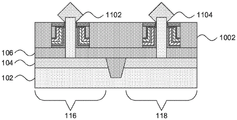
Referring now to fig. 10, a cross-sectional view of a step of forming vertical transistors with equal gate thickness is shown. A layer of dielectric fill is deposited over the first region 116 and the second region 118. It is specifically contemplated that the dielectric fill may be formed of, for example, silicon dioxide, but any suitable dielectric material may be used. The fin mask 114, dielectric fill, and spacers 802 are etched to expose a top portion of the channel fin 112, leaving a dielectric layer 1002 between the first region 116 and the second region 118.
Referring now to fig. 11, a cross-sectional view of a step of forming vertical transistors with equal gate thickness is shown. Top source/ drain regions 1102 and 1104 are formed on top portions of the channel fins 112. It is specifically contemplated that the top source/ drain regions 1102 and 1104 may be epitaxially grown and may have the same basic composition as the channel fin 112 and the bottom source/drain layer 104, but it should be understood that the top source/ drain regions 1102 and 1104 may be formed of any suitable material and may be formed by any suitable process.
N-type source/drain regions 1102 are formed in the first region 116 and p-type source/drain regions 1104 are formed in the second region 118. It should be appreciated that the respective source/drain regions 1104 are doped with an appropriate n-type or p-type dopant, either by in-situ doping or by implantation.
Referring now to fig. 12, a cross-sectional view of a step of forming vertical transistors with equal gate thickness is shown. The interlayer dielectric 1202 is formed of, for example, silicon dioxide, with the dielectric fill layer 1002 extending above the height of the top source/ drain regions 1102 and 1104. Conductive contacts 1204 are then formed through the interlayer dielectric 1202 to contact the top source/ drain regions 1102 and 1104 and the bottom source/drain region 104. The conductive contacts may be formed of any suitable conductive material, including, for example, tungsten, nickel, titanium, molybdenum, tantalum, copper, platinum, silver, gold, ruthenium, iridium, rhenium, rhodium, and alloys thereof.
Referring now to fig. 13, a cross-sectional view of an alternative embodiment of a vertical transistor having an equal gate thickness is shown. In this embodiment, the gate stack connecting the two regions 116 and 118 is not etched away, leaving a conductive connection between the two regions. In this way, devices in both regions can be triggered by a single shared gate. This may be achieved by adding a mask in the region between the two regions before forming the spacers 802.
Referring now to fig. 14, a cross-sectional view of a step of forming an alternate embodiment vertical transistor having an equal gate thickness is shown. This embodiment includes an additional step prior to the step of fig. 4, in which an additional layer 1402 is formed in the n-type workfunction metal stack. The additional layer 1402 may be formed of, for example, titanium nitride. In this embodiment, the titanium nitride matching layer 402 (which matches the thickness of the gate stack in the first region 116 to the thickness of the gate stack in the second region 118) may instead be formed of a conductor such as tungsten or cobalt for the matching layer 1404. This embodiment may then be formed into n-type and p-type transistor devices having separate or common gate structures as described above.
Referring now to fig. 15, a cross-sectional view of a step of forming an alternate embodiment vertical transistor having an equal gate thickness is shown. This embodiment begins with the formation of an n-type workfunction metal stack and the use of a scavenging layer in the second region 118. The n-type workfunction metal stack is formed from, for example, titanium nitride layer 1502, titanium aluminide carbon layer 1504, and titanium nitride layer 1506. After the layer is deposited, the stack is patterned to be confined on the first area 116.
A p-type work function layer 1508 is then deposited over regions 116 and 118, where the p-type work function layer 1508 is formed of, for example, titanium nitride. A scavenging layer 1510 is formed over the p-type work function layer 1508. Then, the matching layer 1512 is formed in the second region 118 from, for example, silicon nitride, such that the thickness of the layer stack in the second region 118 is equal to the thickness of the layer stack in the first region 116. The removal layer 1510 may be formed of, for example, titanium aluminum carbide, and blocks diffusion of oxygen from outside the gate or removes oxygen from the p-type work function layer 1508.
Referring now to fig. 16, a cross-sectional view of a step of forming an alternate embodiment vertical transistor having an equal gate thickness is shown. As shown in fig. 15, an n-type workfunction metal stack is formed in the first region 116. A layer of, for example, titanium nitride 1508 and a removal layer 1510 are then deposited over regions 116 and 118.
A thin layer 1602 of, for example, titanium nitride is deposited over both regions, followed by the formation of a matching layer 1604 in the second region 118, the matching layer 1604 being formed of, for example, cobalt or tungsten. As in other embodiments, matching layer 1604 matches the thickness of the gate stacks in second region 118 to the thickness of the gate stacks in first region 116.
It should be understood that aspects of the present invention will be described in terms of a given illustrative architecture; however, other architectures, structures, substrate materials, and process features and steps may vary within the scope of aspects of the invention.
It will also be understood that when an element such as a layer, region or substrate is referred to as being "on" or "over" another element, it can be directly on the other element or intervening elements may also be present. In contrast, when an element is referred to as being "directly on" or "directly over" another element, there are no intervening elements present. It will also be understood that when an element is referred to as being "connected" or "coupled" to another element, it can be directly connected or coupled to the other element or intervening elements may be present. In contrast, when an element is referred to as being "directly connected" or "directly coupled" to another element, there are no intervening elements present.
The present embodiments may include a design for an integrated circuit chip that may be created in a graphical computer programming language and stored on a computer storage medium (such as a disk, tape, physical hard drive, or virtual hard drive such as in a storage access network). If the designer does not fabricate chips or the photolithographic masks used to fabricate chips, the designer may transmit the resulting design by physical means (e.g., by providing a copy of the storage medium storing the design) or electronically (e.g., through the Internet) to such entities, directly or indirectly. The stored design is then converted into the appropriate format (e.g., GDSII) for the fabrication of photolithographic masks, which typically include multiple copies of the chip design in question that are to be formed on a wafer. A photolithographic mask is utilized to define areas of the wafer (and/or the layers thereon) to be etched or otherwise processed.
The methods as described herein may be used to fabricate integrated circuit chips. The resulting integrated circuit chips may be distributed by the manufacturer in raw wafer form (i.e., as a single wafer having a plurality of unpackaged chips), bare chip, or packaged form. In the latter case, the chips are mounted in a single chip package (such as a plastic carrier with leads affixed to a motherboard or other higher level carrier) or a multi-chip package (such as a ceramic carrier with any surface interconnect or interconnects buried). In any case, the chip is then integrated with other chips, discrete circuit elements, and/or other signal processing devices as part of either (a) an intermediate product, such as a motherboard, or (b) an end product. The end product may be any product that includes integrated circuit chips, ranging from toys and other low-end applications to advanced computer products having a display, a keyboard or other input device, and a central processor.
Should also be treatedThe material composition will be described with reference to the listed components (e.g., SiGe). These compounds include different proportions of elements in the compound, e.g. SiGe includes Si where x is less than or equal to 1xGe1-xAnd the like. In addition, other elements may be included in the compounds and still function in accordance with the principles of the present invention. Compounds with additional elements are referred to herein as alloys.
Reference in the specification to "one embodiment" or "an embodiment" as well as other variations means that a particular feature, structure, characteristic, etc. described in connection with the embodiment is included in at least one embodiment. Thus, the appearances of the phrases "in one embodiment" or "in an embodiment" and any other variations appearing in various places throughout the specification are not necessarily all referring to the same embodiment.
It should be understood that, for example, in the case of "a/B", "a and/or B" and "at least one of a and B", the use of any of the following "/", "and/or" and "at least one" is intended to include the selection of only the first listed option (a), or only the second listed option (B), or both options (a and B). As another example, in the case of "a, B and/or C" and "at least one of a, B and C", such wording is intended to include selecting only the first listed option (a), or only the second listed option (B), or only the third listed option (C), or only the first and second listed options (a and B), or only the first and third listed options (a and C), or only the second and third listed options (B and C), or all three options (a and B and C). This can be extended for many of the items listed, as will be apparent to those of ordinary skill in this and related arts.
The terminology used herein is for the purpose of describing particular embodiments only and is not intended to be limiting of example embodiments. As used herein, the singular forms "a", "an" and "the" are intended to include the plural forms as well, unless the context clearly indicates otherwise. It will be further understood that the terms "comprises," "comprising," "includes" and/or "including," when used herein, specify the presence of stated features, integers, steps, operations, elements, and/or components, but do not preclude the presence or addition of one or more other features, integers, steps, operations, elements, components, and/or groups thereof.
Spatially relative terms, such as "below", "lower", "above", "upper", and the like, may be used herein for convenience in describing the relationship of one element or feature to other element(s) or feature(s) as illustrated in the figures. It will be understood that the spatially relative terms are intended to encompass different orientations of the device in use or operation in addition to the orientation depicted in the figures. For example, if the device in the figures is turned over, elements described as "below" or "beneath" other elements or features would then be oriented "above" the other elements or features. Thus, the term "below" may include both an orientation of above and below. The device may be otherwise oriented (rotated 90 degrees or at other orientations) and the spatially relative descriptors used herein interpreted accordingly. In addition, it will also be understood that when a layer is referred to as being "between" two layers, it can be the only layer between the two layers, or one or more intervening layers may also be present.
It will be understood that, although the terms first, second, etc. may be used herein to describe various elements, these elements should not be limited by these terms. These terms are only used to distinguish one element from another. Thus, a first element discussed below could be termed a second element without departing from the scope of the present concept.
Referring now to fig. 17, a method of forming a transistor is shown. Block 1702 forms a vertical channel 112 on the lower source/drain layer 104. The lower source/drain layer 104 may be divided into different regions, including a first region 116 and a second region 118, in each of which a respective vertical channel 112 is formed. Block 1703 forms a gate dielectric 110 over the vertical channel 112, particularly forming the gate dielectric 110 on sidewalls of the vertical channel 112.
In one embodiment, the first type of work function layer may be a p-type titanium nitride layer formed in the p-type region 118. In another embodiment, the first type of work function layer may be an n-type stack comprising an n-type titanium nitride layer and a titanium aluminum carbon layer and optionally a second titanium nitride layer, the n-type stack being formed in the n-type region 116.
Block 1708 forms a thickness matching layer in the region without the work function layer of the first type. The thickness of the matching layer is substantially equal to the thickness of the first type work function layer such that the thickness of the stack in the two regions is substantially equal. In one embodiment, the matching layer may be formed of titanium nitride. In another embodiment, the matching layer may be formed of a metal conductor such as cobalt or tungsten.
Block 1716 etches the spacers 802 to expose top portions of the vertical channels 112. Block 1718 forms top source/ drain regions 1102 and 1104 on top portions of the vertical channels 112. It is specifically contemplated that the top source/ drain regions 1102 and 1104 may be formed by epitaxial growth in which dopants appropriate for the respective device type of each region are doped in situ. Block 1720 completes the device, forming interlayer dielectric 1202 and electrical contacts 1204 to the top and bottom source/drain regions and gates.
Having described preferred embodiments for a vertical pass transistor with equal gate stack thickness (which are intended to be illustrative and not limiting), it is noted that modifications and variations can be made by persons skilled in the art in light of the above teachings. It is therefore to be understood that changes may be made in the particular embodiments disclosed which are within the scope of the invention as outlined by the appended claims.
Claims (20)
1. A method of forming a semiconductor device, comprising:
forming a vertical semiconductor channel on the bottom source/drain layer in the first type region and the second type region;
forming a gate dielectric layer on sidewalls of the vertical semiconductor channel;
forming a first-type work function layer in the first-type region;
forming a second-type work function layer in both the first-type region and the second-type region;
forming a thickness matching layer in the second type region such that the layer stack in the first type region has the same thickness as the layer stack in the second type region; and
a top source/drain region is formed at a top portion of the vertical channel.
2. The method of claim 1, further comprising forming a scavenging layer on the second-type work function layer.
3. The method according to claim 1, wherein a portion of the first and second work function layers in a region between the first and second type regions is retained.
4. The method of claim 1, further comprising recessing a first type stack formed from the first type work function layer and the second type work function layer and a second type stack formed from the second type work function layer and the thickness matching layer below a height of the vertical semiconductor channel.
5. The method of claim 4, further comprising forming spacers on exposed sidewalls of the vertical semiconductor channel.
6. The method of claim 5, further comprising etching away a portion of the first and second work function layer types from a region between the first and second type regions.
7. The method of claim 5, further comprising etching back the spacers prior to forming the top source/drain regions.
8. The method of claim 1, wherein the thickness matching layer comprises titanium nitride.
9. The method of claim 1, wherein the thickness matching layer comprises a material selected from the group consisting of cobalt and tungsten.
10. A method for forming a semiconductor device, comprising:
forming a vertical semiconductor channel on the bottom source/drain layer in the first type region and the second type region;
forming a gate dielectric layer on sidewalls of the vertical semiconductor channel;
forming a first-type work function layer in the first-type region;
forming a second-type work function layer in both the first-type region and the second-type region;
forming a thickness matching layer in the second type region such that the layer stack in the first type region has the same thickness as the layer stack in the second type region;
recessing a first type stack formed from the first type work function layer and the second type work function layer and a second type stack formed from the second type work function layer and the thickness matching layer below a height of the vertical semiconductor channel;
forming spacers on exposed sidewalls of the vertical semiconductor channel;
etching back the spacers to expose a top portion of each vertical channel; and
forming a top source/drain region on the top portion of the vertical channel.
11. An integrated chip, comprising:
a first semiconductor device of a first type, the first semiconductor device comprising:
a vertical semiconductor channel;
a gate dielectric layer formed on sidewalls of the vertical semiconductor channel;
a first-type work function layer formed on the gate dielectric layer; and
a second-type work function layer formed later on said first-type work function; and a second semiconductor device of a second type, the second semiconductor device comprising:
a vertical semiconductor channel;
a gate dielectric layer formed on sidewalls of the vertical semiconductor channel;
a second-type work function layer formed on the gate dielectric layer; and
a thickness matching layer formed on the second-type work function layer, the thickness matching layer having a thickness substantially equal to a thickness of the first-type work function layer.
12. The integrated chip of claim 11, further comprising an inter-device connection connecting the first and second semiconductor devices and comprising portions of the first-type work function layer, the second-type work function layer, and the thickness matching layer.
13. The integrated chip of claim 11, wherein the first semiconductor device is an n-type transistor, and wherein the second semiconductor device is a p-type transistor.
14. The integrated chip of claim 13, wherein the first work function layer type comprises an n-type titanium nitride layer, a titanium aluminum carbon layer, and a second titanium nitride layer, and wherein the second work function layer type comprises a p-type titanium nitride layer.
15. The integrated chip of claim 13, wherein the first semiconductor device further comprises a scavenging layer on the second-type work function layer, and wherein the second semiconductor device further comprises a scavenging layer between the second-type work function layer and the thickness matching layer.
16. The integrated chip of claim 15, wherein the thickness matching layer comprises a material selected from the group consisting of titanium nitride, cobalt, and tungsten.
17. The integrated chip of claim 11, wherein the first semiconductor device is a p-type transistor, and wherein the second semiconductor device is an n-type transistor.
18. The integrated chip of claim 17, wherein the first type of work function layer comprises a p-type titanium nitride layer, and wherein the second type of work function layer comprises an n-type titanium nitride layer and a titanium aluminum carbon layer.
19. The integrated chip of claim 17, wherein the thickness matching layer comprises a material selected from the group consisting of titanium nitride, cobalt, and tungsten.
20. The integrated chip of claim 17, wherein the second-type work function layer further comprises a second titanium nitride layer.
Applications Claiming Priority (3)
| Application Number | Priority Date | Filing Date | Title |
|---|---|---|---|
| US15/582,905 | 2017-05-01 | ||
| US15/582,905 US10103147B1 (en) | 2017-05-01 | 2017-05-01 | Vertical transport transistors with equal gate stack thicknesses |
| PCT/IB2018/052586 WO2018203162A1 (en) | 2017-05-01 | 2018-04-13 | Vertical transport transistors with equal gate stack thicknesses |
Publications (2)
| Publication Number | Publication Date |
|---|---|
| CN110892513A true CN110892513A (en) | 2020-03-17 |
| CN110892513B CN110892513B (en) | 2023-08-18 |
Family
ID=63761328
Family Applications (1)
| Application Number | Title | Priority Date | Filing Date |
|---|---|---|---|
| CN201880026997.4A Active CN110892513B (en) | 2017-05-01 | 2018-04-13 | Vertical pass transistor with equal gate stack thickness |
Country Status (6)
| Country | Link |
|---|---|
| US (3) | US10103147B1 (en) |
| JP (1) | JP7004742B2 (en) |
| CN (1) | CN110892513B (en) |
| DE (1) | DE112018002294B4 (en) |
| GB (1) | GB2575933B (en) |
| WO (1) | WO2018203162A1 (en) |
Cited By (1)
| Publication number | Priority date | Publication date | Assignee | Title |
|---|---|---|---|---|
| CN113838802A (en) * | 2020-06-24 | 2021-12-24 | 中芯国际集成电路制造(上海)有限公司 | Semiconductor structure and forming method thereof |
Families Citing this family (6)
| Publication number | Priority date | Publication date | Assignee | Title |
|---|---|---|---|---|
| US10229986B1 (en) * | 2017-12-04 | 2019-03-12 | International Business Machines Corporation | Vertical transport field-effect transistor including dual layer top spacer |
| US10818756B2 (en) * | 2018-11-02 | 2020-10-27 | International Business Machines Corporation | Vertical transport FET having multiple threshold voltages with zero-thickness variation of work function metal |
| CN113053815A (en) * | 2019-12-26 | 2021-06-29 | 中芯国际集成电路制造(上海)有限公司 | Semiconductor device and forming method |
| CN113363211B (en) * | 2020-03-05 | 2023-10-20 | 中芯国际集成电路制造(上海)有限公司 | Semiconductor structure and forming method thereof |
| US11699736B2 (en) | 2020-06-25 | 2023-07-11 | Taiwan Semiconductor Manufacturing Co., Ltd. | Gate structure and method |
| CN113629148A (en) * | 2021-06-24 | 2021-11-09 | 湖南大学 | Double-gate enhanced gallium oxide MESFET device and manufacturing method thereof |
Citations (4)
| Publication number | Priority date | Publication date | Assignee | Title |
|---|---|---|---|---|
| CN102956702A (en) * | 2011-08-31 | 2013-03-06 | 中国科学院微电子研究所 | Semiconductor device and method for manufacturing the same |
| US20150236086A1 (en) * | 2014-02-19 | 2015-08-20 | Taiwan Semiconductor Manufacturing Company Limited | Semiconductor structures and methods for multi-level work function |
| CN105280698A (en) * | 2014-06-30 | 2016-01-27 | 台湾积体电路制造股份有限公司 | Vertical device architecture |
| CN106505104A (en) * | 2015-09-04 | 2017-03-15 | 台湾积体电路制造股份有限公司 | FINFET device and its manufacture method |
Family Cites Families (25)
| Publication number | Priority date | Publication date | Assignee | Title |
|---|---|---|---|---|
| DE10350751B4 (en) | 2003-10-30 | 2008-04-24 | Infineon Technologies Ag | Method for producing a vertical field effect transistor and field effect memory transistor, in particular FLASH memory transistor |
| US7736965B2 (en) | 2007-12-06 | 2010-06-15 | International Business Machines Corporation | Method of making a FinFET device structure having dual metal and high-k gates |
| JP4316657B2 (en) | 2008-01-29 | 2009-08-19 | 日本ユニサンティスエレクトロニクス株式会社 | Semiconductor device |
| US8021949B2 (en) | 2009-12-01 | 2011-09-20 | International Business Machines Corporation | Method and structure for forming finFETs with multiple doping regions on a same chip |
| KR20140106903A (en) * | 2013-02-27 | 2014-09-04 | 에스케이하이닉스 주식회사 | Transistor, Variable Memory Device and Method of Manufacturing The Same |
| US9330937B2 (en) | 2013-11-13 | 2016-05-03 | Intermolecular, Inc. | Etching of semiconductor structures that include titanium-based layers |
| US9105662B1 (en) | 2014-01-23 | 2015-08-11 | International Business Machines Corporation | Method and structure to enhance gate induced strain effect in multigate device |
| KR102212267B1 (en) | 2014-03-19 | 2021-02-04 | 삼성전자주식회사 | Semiconductor device and method for fabricating the same |
| US9941394B2 (en) | 2014-04-30 | 2018-04-10 | Taiwan Semiconductor Manufacturing Co., Ltd. | Tunnel field-effect transistor |
| US10418271B2 (en) | 2014-06-13 | 2019-09-17 | Taiwan Semiconductor Manufacturing Co., Ltd. | Method of forming isolation layer |
| US9831100B2 (en) | 2014-06-24 | 2017-11-28 | Intermolecular, Inc. | Solution based etching of titanium carbide and titanium nitride structures |
| US9786774B2 (en) | 2014-06-27 | 2017-10-10 | Taiwan Semiconductor Manufacturing Company, Ltd. | Metal gate of gate-all-around transistor |
| US9318447B2 (en) | 2014-07-18 | 2016-04-19 | Taiwan Semiconductor Manufacturing Company Limited | Semiconductor device and method of forming vertical structure |
| US9893159B2 (en) * | 2014-08-15 | 2018-02-13 | Taiwan Semiconductor Manufacturing Co., Ltd. | Transistor, integrated circuit and method of fabricating the same |
| US9985026B2 (en) * | 2014-08-15 | 2018-05-29 | Taiwan Semiconductor Manufacturing Co., Ltd. | Transistor, integrated circuit and method of fabricating the same |
| US9911848B2 (en) | 2014-08-29 | 2018-03-06 | Taiwan Semiconductor Manufacturing Co., Ltd. | Vertical transistor and method of manufacturing the same |
| CN105405886B (en) | 2014-09-10 | 2018-09-07 | 中国科学院微电子研究所 | FinFET structure and manufacturing method thereof |
| CN105513967A (en) | 2014-09-26 | 2016-04-20 | 中芯国际集成电路制造(上海)有限公司 | Transistor forming method |
| KR20160054830A (en) | 2014-11-07 | 2016-05-17 | 삼성전자주식회사 | Method for manufacturing semiconductor device |
| KR102250583B1 (en) * | 2014-12-16 | 2021-05-12 | 에스케이하이닉스 주식회사 | Semiconductor device having dual work function gate structure and method for manufacturing the same, memory cell having the same and electronic device having the same |
| KR102242989B1 (en) * | 2014-12-16 | 2021-04-22 | 에스케이하이닉스 주식회사 | Semiconductor device having dual work function gate structure and method for manufacturing the same, memory cell having the same and electronic device having the same |
| US9343372B1 (en) | 2014-12-29 | 2016-05-17 | GlobalFoundries, Inc. | Metal stack for reduced gate resistance |
| US9349860B1 (en) * | 2015-03-31 | 2016-05-24 | Taiwan Semiconductor Manufacturing Company, Ltd. | Field effect transistors and methods of forming same |
| US9553092B2 (en) | 2015-06-12 | 2017-01-24 | Globalfoundries Inc. | Alternative threshold voltage scheme via direct metal gate patterning for high performance CMOS FinFETs |
| CN106601605B (en) | 2015-10-19 | 2020-02-28 | 中芯国际集成电路制造(北京)有限公司 | Gate stack structure, NMOS device, semiconductor device and manufacturing method thereof |
-
2017
- 2017-05-01 US US15/582,905 patent/US10103147B1/en active Active
- 2017-11-08 US US15/806,759 patent/US10157923B2/en active Active
-
2018
- 2018-04-13 GB GB1915589.4A patent/GB2575933B/en active Active
- 2018-04-13 DE DE112018002294.3T patent/DE112018002294B4/en active Active
- 2018-04-13 WO PCT/IB2018/052586 patent/WO2018203162A1/en active Application Filing
- 2018-04-13 JP JP2019555688A patent/JP7004742B2/en active Active
- 2018-04-13 CN CN201880026997.4A patent/CN110892513B/en active Active
- 2018-08-08 US US16/058,173 patent/US10312237B2/en active Active
Patent Citations (4)
| Publication number | Priority date | Publication date | Assignee | Title |
|---|---|---|---|---|
| CN102956702A (en) * | 2011-08-31 | 2013-03-06 | 中国科学院微电子研究所 | Semiconductor device and method for manufacturing the same |
| US20150236086A1 (en) * | 2014-02-19 | 2015-08-20 | Taiwan Semiconductor Manufacturing Company Limited | Semiconductor structures and methods for multi-level work function |
| CN105280698A (en) * | 2014-06-30 | 2016-01-27 | 台湾积体电路制造股份有限公司 | Vertical device architecture |
| CN106505104A (en) * | 2015-09-04 | 2017-03-15 | 台湾积体电路制造股份有限公司 | FINFET device and its manufacture method |
Cited By (2)
| Publication number | Priority date | Publication date | Assignee | Title |
|---|---|---|---|---|
| CN113838802A (en) * | 2020-06-24 | 2021-12-24 | 中芯国际集成电路制造(上海)有限公司 | Semiconductor structure and forming method thereof |
| CN113838802B (en) * | 2020-06-24 | 2023-10-17 | 中芯国际集成电路制造(上海)有限公司 | Semiconductor structure and forming method thereof |
Also Published As
| Publication number | Publication date |
|---|---|
| GB2575933B (en) | 2021-09-29 |
| DE112018002294B4 (en) | 2023-05-17 |
| US20180315756A1 (en) | 2018-11-01 |
| US10157923B2 (en) | 2018-12-18 |
| US10103147B1 (en) | 2018-10-16 |
| US20180315755A1 (en) | 2018-11-01 |
| WO2018203162A1 (en) | 2018-11-08 |
| JP7004742B2 (en) | 2022-01-21 |
| JP2020519006A (en) | 2020-06-25 |
| US10312237B2 (en) | 2019-06-04 |
| US20180350811A1 (en) | 2018-12-06 |
| GB201915589D0 (en) | 2019-12-11 |
| GB2575933A (en) | 2020-01-29 |
| DE112018002294T5 (en) | 2020-02-13 |
| CN110892513B (en) | 2023-08-18 |
Similar Documents
| Publication | Publication Date | Title |
|---|---|---|
| US11101182B2 (en) | Nanosheet transistors with different gate dielectrics and workfunction metals | |
| US10263075B2 (en) | Nanosheet CMOS transistors | |
| CN110892513B (en) | Vertical pass transistor with equal gate stack thickness | |
| US11515214B2 (en) | Threshold voltage adjustment by inner spacer material selection | |
| US10777469B2 (en) | Self-aligned top spacers for vertical FETs with in situ solid state doping | |
| US11764265B2 (en) | Nanosheet transistor with inner spacers | |
| US12100746B2 (en) | Gate-all-around field effect transistor with bottom dielectric isolation | |
| US12087770B2 (en) | Complementary field effect transistor devices | |
| US11444165B2 (en) | Asymmetric threshold voltages in semiconductor devices | |
| US11791342B2 (en) | Varactor integrated with complementary metal-oxide semiconductor devices | |
| US11489044B2 (en) | Nanosheet transistor bottom isolation | |
| US12107014B2 (en) | Nanosheet transistors with self-aligned gate cut | |
| US20230197814A1 (en) | Hybrid gate cut for stacked transistors | |
| US11769796B2 (en) | Hybrid complementary metal-oxide semiconductor field effect transistor nanosheet device | |
| US12107147B2 (en) | Self-aligned gate contact for VTFETs |
Legal Events
| Date | Code | Title | Description |
|---|---|---|---|
| PB01 | Publication | ||
| PB01 | Publication | ||
| SE01 | Entry into force of request for substantive examination | ||
| SE01 | Entry into force of request for substantive examination | ||
| GR01 | Patent grant | ||
| GR01 | Patent grant |