CN103578786A - Conductive layered structure, electrode, supercapacitor, method of manufacturing the conductive layered structure, and electronic device in a body - Google Patents
Conductive layered structure, electrode, supercapacitor, method of manufacturing the conductive layered structure, and electronic device in a body Download PDFInfo
- Publication number
- CN103578786A CN103578786A CN201310320476.9A CN201310320476A CN103578786A CN 103578786 A CN103578786 A CN 103578786A CN 201310320476 A CN201310320476 A CN 201310320476A CN 103578786 A CN103578786 A CN 103578786A
- Authority
- CN
- China
- Prior art keywords
- electrode
- dna
- dna hydrogel
- laminated structure
- layer
- Prior art date
- Legal status (The legal status is an assumption and is not a legal conclusion. Google has not performed a legal analysis and makes no representation as to the accuracy of the status listed.)
- Pending
Links
- 238000004519 manufacturing process Methods 0.000 title claims abstract description 52
- 239000000017 hydrogel Substances 0.000 claims abstract description 156
- 239000002131 composite material Substances 0.000 claims abstract description 83
- 239000004020 conductor Substances 0.000 claims abstract description 57
- 238000000034 method Methods 0.000 claims abstract description 54
- 239000010410 layer Substances 0.000 claims description 186
- 108020004414 DNA Proteins 0.000 claims description 185
- 229920000642 polymer Polymers 0.000 claims description 81
- 229920000867 polyelectrolyte Polymers 0.000 claims description 69
- 238000002360 preparation method Methods 0.000 claims description 52
- 229920000767 polyaniline Polymers 0.000 claims description 51
- OKTJSMMVPCPJKN-UHFFFAOYSA-N Carbon Chemical compound [C] OKTJSMMVPCPJKN-UHFFFAOYSA-N 0.000 claims description 35
- 239000000243 solution Substances 0.000 claims description 35
- 229920000371 poly(diallyldimethylammonium chloride) polymer Polymers 0.000 claims description 27
- 239000002109 single walled nanotube Substances 0.000 claims description 25
- 229920001940 conductive polymer Polymers 0.000 claims description 24
- 239000003792 electrolyte Substances 0.000 claims description 22
- 229920002518 Polyallylamine hydrochloride Polymers 0.000 claims description 21
- 239000002322 conducting polymer Substances 0.000 claims description 21
- 239000007864 aqueous solution Substances 0.000 claims description 18
- 239000002041 carbon nanotube Substances 0.000 claims description 18
- 229910021393 carbon nanotube Inorganic materials 0.000 claims description 18
- 238000004108 freeze drying Methods 0.000 claims description 17
- 239000007772 electrode material Substances 0.000 claims description 16
- 229920002125 Sokalan® Polymers 0.000 claims description 15
- 238000005406 washing Methods 0.000 claims description 15
- XLYOFNOQVPJJNP-UHFFFAOYSA-N water Substances O XLYOFNOQVPJJNP-UHFFFAOYSA-N 0.000 claims description 15
- 238000007598 dipping method Methods 0.000 claims description 14
- -1 amino-2-ethyl Chemical group 0.000 claims description 10
- 229910052751 metal Inorganic materials 0.000 claims description 10
- 239000002184 metal Substances 0.000 claims description 10
- BASFCYQUMIYNBI-UHFFFAOYSA-N platinum Chemical compound [Pt] BASFCYQUMIYNBI-UHFFFAOYSA-N 0.000 claims description 10
- 229920001897 terpolymer Polymers 0.000 claims description 10
- 230000009467 reduction Effects 0.000 claims description 9
- 239000000758 substrate Substances 0.000 claims description 9
- YTPLMLYBLZKORZ-UHFFFAOYSA-N Thiophene Chemical compound C=1C=CSC=1 YTPLMLYBLZKORZ-UHFFFAOYSA-N 0.000 claims description 8
- UHOVQNZJYSORNB-UHFFFAOYSA-N monobenzene Natural products C1=CC=CC=C1 UHOVQNZJYSORNB-UHFFFAOYSA-N 0.000 claims description 8
- 238000005660 chlorination reaction Methods 0.000 claims description 5
- YIOJGTBNHQAVBO-UHFFFAOYSA-N dimethyl-bis(prop-2-enyl)azanium Chemical compound C=CC[N+](C)(C)CC=C YIOJGTBNHQAVBO-UHFFFAOYSA-N 0.000 claims description 5
- 229910052697 platinum Inorganic materials 0.000 claims description 5
- NOWKCMXCCJGMRR-UHFFFAOYSA-N Aziridine Chemical compound C1CN1 NOWKCMXCCJGMRR-UHFFFAOYSA-N 0.000 claims description 4
- 241000790917 Dioxys <bee> Species 0.000 claims description 4
- 229920002678 cellulose Polymers 0.000 claims description 4
- 239000001913 cellulose Substances 0.000 claims description 4
- 239000008151 electrolyte solution Substances 0.000 claims description 4
- 239000010931 gold Substances 0.000 claims description 4
- 229910021389 graphene Inorganic materials 0.000 claims description 4
- 238000009434 installation Methods 0.000 claims description 4
- 239000011241 protective layer Substances 0.000 claims description 4
- 159000000000 sodium salts Chemical class 0.000 claims description 4
- 229930192474 thiophene Natural products 0.000 claims description 4
- 239000010936 titanium Substances 0.000 claims description 4
- 102000053602 DNA Human genes 0.000 claims description 3
- XEEYBQQBJWHFJM-UHFFFAOYSA-N Iron Chemical compound [Fe] XEEYBQQBJWHFJM-UHFFFAOYSA-N 0.000 claims description 3
- 239000004698 Polyethylene Substances 0.000 claims description 3
- 239000004743 Polypropylene Substances 0.000 claims description 3
- 108020004682 Single-Stranded DNA Proteins 0.000 claims description 3
- 239000004809 Teflon Substances 0.000 claims description 3
- 229920006362 Teflon® Polymers 0.000 claims description 3
- RTAQQCXQSZGOHL-UHFFFAOYSA-N Titanium Chemical compound [Ti] RTAQQCXQSZGOHL-UHFFFAOYSA-N 0.000 claims description 3
- 230000015572 biosynthetic process Effects 0.000 claims description 3
- PCHJSUWPFVWCPO-UHFFFAOYSA-N gold Chemical group [Au] PCHJSUWPFVWCPO-UHFFFAOYSA-N 0.000 claims description 3
- 229910052737 gold Inorganic materials 0.000 claims description 3
- 238000009396 hybridization Methods 0.000 claims description 3
- 229920000573 polyethylene Polymers 0.000 claims description 3
- 229920001155 polypropylene Polymers 0.000 claims description 3
- 229920000128 polypyrrole Polymers 0.000 claims description 3
- 229920000123 polythiophene Polymers 0.000 claims description 3
- KWYUFKZDYYNOTN-UHFFFAOYSA-M potassium hydroxide Inorganic materials [OH-].[K+] KWYUFKZDYYNOTN-UHFFFAOYSA-M 0.000 claims description 3
- 229910052709 silver Inorganic materials 0.000 claims description 3
- 239000011734 sodium Substances 0.000 claims description 3
- 229910052719 titanium Inorganic materials 0.000 claims description 3
- IBZJNLWLRUHZIX-UHFFFAOYSA-N 1-ethyl-3-methyl-2h-imidazole Chemical compound CCN1CN(C)C=C1 IBZJNLWLRUHZIX-UHFFFAOYSA-N 0.000 claims description 2
- 229910013870 LiPF 6 Inorganic materials 0.000 claims description 2
- BQCADISMDOOEFD-UHFFFAOYSA-N Silver Chemical compound [Ag] BQCADISMDOOEFD-UHFFFAOYSA-N 0.000 claims description 2
- 210000005252 bulbus oculi Anatomy 0.000 claims description 2
- 150000002466 imines Chemical class 0.000 claims description 2
- 238000007654 immersion Methods 0.000 claims description 2
- MHCFAGZWMAWTNR-UHFFFAOYSA-M lithium perchlorate Chemical compound [Li+].[O-]Cl(=O)(=O)=O MHCFAGZWMAWTNR-UHFFFAOYSA-M 0.000 claims description 2
- 229910001486 lithium perchlorate Inorganic materials 0.000 claims description 2
- 229910001496 lithium tetrafluoroborate Inorganic materials 0.000 claims description 2
- WCUXLLCKKVVCTQ-UHFFFAOYSA-M potassium chloride Inorganic materials [Cl-].[K+] WCUXLLCKKVVCTQ-UHFFFAOYSA-M 0.000 claims description 2
- 239000004332 silver Substances 0.000 claims description 2
- 238000002955 isolation Methods 0.000 claims 1
- 230000008569 process Effects 0.000 abstract description 16
- 239000005518 polymer electrolyte Substances 0.000 abstract 1
- 238000013461 design Methods 0.000 description 35
- 238000001878 scanning electron micrograph Methods 0.000 description 23
- 239000007943 implant Substances 0.000 description 21
- LOKCTEFSRHRXRJ-UHFFFAOYSA-I dipotassium trisodium dihydrogen phosphate hydrogen phosphate dichloride Chemical compound P(=O)(O)(O)[O-].[K+].P(=O)(O)([O-])[O-].[Na+].[Na+].[Cl-].[K+].[Cl-].[Na+] LOKCTEFSRHRXRJ-UHFFFAOYSA-I 0.000 description 20
- 239000002953 phosphate buffered saline Substances 0.000 description 20
- 239000006143 cell culture medium Substances 0.000 description 16
- 238000002484 cyclic voltammetry Methods 0.000 description 16
- 238000012360 testing method Methods 0.000 description 15
- 239000003990 capacitor Substances 0.000 description 12
- 210000004027 cell Anatomy 0.000 description 10
- 239000012153 distilled water Substances 0.000 description 10
- 210000000056 organ Anatomy 0.000 description 9
- 229920001609 Poly(3,4-ethylenedioxythiophene) Polymers 0.000 description 8
- QAOWNCQODCNURD-UHFFFAOYSA-N Sulfuric acid Chemical compound OS(O)(=O)=O QAOWNCQODCNURD-UHFFFAOYSA-N 0.000 description 8
- 230000004087 circulation Effects 0.000 description 8
- 210000004927 skin cell Anatomy 0.000 description 8
- HFQQZARZPUDIFP-UHFFFAOYSA-M sodium;2-dodecylbenzenesulfonate Chemical compound [Na+].CCCCCCCCCCCCC1=CC=CC=C1S([O-])(=O)=O HFQQZARZPUDIFP-UHFFFAOYSA-M 0.000 description 8
- 238000010586 diagram Methods 0.000 description 6
- 150000002500 ions Chemical class 0.000 description 6
- 239000000463 material Substances 0.000 description 6
- 230000008859 change Effects 0.000 description 5
- 239000011248 coating agent Substances 0.000 description 5
- 238000000576 coating method Methods 0.000 description 5
- WZFUQSJFWNHZHM-UHFFFAOYSA-N 2-[4-[2-(2,3-dihydro-1H-inden-2-ylamino)pyrimidin-5-yl]piperazin-1-yl]-1-(2,4,6,7-tetrahydrotriazolo[4,5-c]pyridin-5-yl)ethanone Chemical compound C1C(CC2=CC=CC=C12)NC1=NC=C(C=N1)N1CCN(CC1)CC(=O)N1CC2=C(CC1)NN=N2 WZFUQSJFWNHZHM-UHFFFAOYSA-N 0.000 description 4
- 238000001237 Raman spectrum Methods 0.000 description 4
- 238000003917 TEM image Methods 0.000 description 4
- 238000007599 discharging Methods 0.000 description 4
- 238000011156 evaluation Methods 0.000 description 4
- 210000002700 urine Anatomy 0.000 description 4
- WEVYAHXRMPXWCK-UHFFFAOYSA-N Acetonitrile Chemical group CC#N WEVYAHXRMPXWCK-UHFFFAOYSA-N 0.000 description 3
- FAPWRFPIFSIZLT-UHFFFAOYSA-M Sodium chloride Chemical compound [Na+].[Cl-] FAPWRFPIFSIZLT-UHFFFAOYSA-M 0.000 description 3
- 239000003575 carbonaceous material Substances 0.000 description 3
- KRKNYBCHXYNGOX-UHFFFAOYSA-N citric acid Chemical compound OC(=O)CC(O)(C(O)=O)CC(O)=O KRKNYBCHXYNGOX-UHFFFAOYSA-N 0.000 description 3
- 230000000694 effects Effects 0.000 description 3
- 230000005518 electrochemistry Effects 0.000 description 3
- 230000014759 maintenance of location Effects 0.000 description 3
- 239000007758 minimum essential medium Substances 0.000 description 3
- 125000002467 phosphate group Chemical group [H]OP(=O)(O[H])O[*] 0.000 description 3
- 239000002904 solvent Substances 0.000 description 3
- 230000001988 toxicity Effects 0.000 description 3
- 231100000419 toxicity Toxicity 0.000 description 3
- CSCPPACGZOOCGX-UHFFFAOYSA-N Acetone Chemical compound CC(C)=O CSCPPACGZOOCGX-UHFFFAOYSA-N 0.000 description 2
- NLXLAEXVIDQMFP-UHFFFAOYSA-N Ammonia chloride Chemical compound [NH4+].[Cl-] NLXLAEXVIDQMFP-UHFFFAOYSA-N 0.000 description 2
- CSNNHWWHGAXBCP-UHFFFAOYSA-L Magnesium sulfate Chemical compound [Mg+2].[O-][S+2]([O-])([O-])[O-] CSNNHWWHGAXBCP-UHFFFAOYSA-L 0.000 description 2
- PXHVJJICTQNCMI-UHFFFAOYSA-N Nickel Chemical compound [Ni] PXHVJJICTQNCMI-UHFFFAOYSA-N 0.000 description 2
- CDBYLPFSWZWCQE-UHFFFAOYSA-L Sodium Carbonate Chemical compound [Na+].[Na+].[O-]C([O-])=O CDBYLPFSWZWCQE-UHFFFAOYSA-L 0.000 description 2
- PMZURENOXWZQFD-UHFFFAOYSA-L Sodium Sulfate Chemical compound [Na+].[Na+].[O-]S([O-])(=O)=O PMZURENOXWZQFD-UHFFFAOYSA-L 0.000 description 2
- XSQUKJJJFZCRTK-UHFFFAOYSA-N Urea Chemical compound NC(N)=O XSQUKJJJFZCRTK-UHFFFAOYSA-N 0.000 description 2
- 150000001450 anions Chemical class 0.000 description 2
- 150000001768 cations Chemical class 0.000 description 2
- 230000005779 cell damage Effects 0.000 description 2
- 201000010099 disease Diseases 0.000 description 2
- 208000037265 diseases, disorders, signs and symptoms Diseases 0.000 description 2
- 239000006185 dispersion Substances 0.000 description 2
- 238000002513 implantation Methods 0.000 description 2
- JVTAAEKCZFNVCJ-UHFFFAOYSA-N lactic acid Chemical compound CC(O)C(O)=O JVTAAEKCZFNVCJ-UHFFFAOYSA-N 0.000 description 2
- 238000005259 measurement Methods 0.000 description 2
- 230000029052 metamorphosis Effects 0.000 description 2
- 239000002048 multi walled nanotube Substances 0.000 description 2
- 238000011160 research Methods 0.000 description 2
- 239000000523 sample Substances 0.000 description 2
- 238000000926 separation method Methods 0.000 description 2
- 239000010802 sludge Substances 0.000 description 2
- 239000002002 slurry Substances 0.000 description 2
- 238000004611 spectroscopical analysis Methods 0.000 description 2
- NVKHKMBMLSFNNU-UHFFFAOYSA-N C=CC1=CC=CC=C1.[S] Chemical compound C=CC1=CC=CC=C1.[S] NVKHKMBMLSFNNU-UHFFFAOYSA-N 0.000 description 1
- UXVMQQNJUSDDNG-UHFFFAOYSA-L Calcium chloride Chemical compound [Cl-].[Cl-].[Ca+2] UXVMQQNJUSDDNG-UHFFFAOYSA-L 0.000 description 1
- 241000282693 Cercopithecidae Species 0.000 description 1
- RYGMFSIKBFXOCR-UHFFFAOYSA-N Copper Chemical compound [Cu] RYGMFSIKBFXOCR-UHFFFAOYSA-N 0.000 description 1
- 102000012410 DNA Ligases Human genes 0.000 description 1
- 108010061982 DNA Ligases Proteins 0.000 description 1
- 239000006144 Dulbecco’s modified Eagle's medium Substances 0.000 description 1
- 239000012594 Earle’s Balanced Salt Solution Substances 0.000 description 1
- 102000003960 Ligases Human genes 0.000 description 1
- 108090000364 Ligases Proteins 0.000 description 1
- HBBGRARXTFLTSG-UHFFFAOYSA-N Lithium ion Chemical compound [Li+] HBBGRARXTFLTSG-UHFFFAOYSA-N 0.000 description 1
- 229920000144 PEDOT:PSS Polymers 0.000 description 1
- 229930182555 Penicillin Natural products 0.000 description 1
- JGSARLDLIJGVTE-MBNYWOFBSA-N Penicillin G Chemical compound N([C@H]1[C@H]2SC([C@@H](N2C1=O)C(O)=O)(C)C)C(=O)CC1=CC=CC=C1 JGSARLDLIJGVTE-MBNYWOFBSA-N 0.000 description 1
- 238000010521 absorption reaction Methods 0.000 description 1
- 239000002253 acid Substances 0.000 description 1
- 230000002378 acidificating effect Effects 0.000 description 1
- 239000000853 adhesive Substances 0.000 description 1
- 230000001070 adhesive effect Effects 0.000 description 1
- 239000000956 alloy Substances 0.000 description 1
- 229910045601 alloy Inorganic materials 0.000 description 1
- 238000005275 alloying Methods 0.000 description 1
- 239000004411 aluminium Substances 0.000 description 1
- 229910052782 aluminium Inorganic materials 0.000 description 1
- XAGFODPZIPBFFR-UHFFFAOYSA-N aluminium Chemical compound [Al] XAGFODPZIPBFFR-UHFFFAOYSA-N 0.000 description 1
- 235000019270 ammonium chloride Nutrition 0.000 description 1
- 230000003321 amplification Effects 0.000 description 1
- 239000011230 binding agent Substances 0.000 description 1
- 239000000560 biocompatible material Substances 0.000 description 1
- 239000006227 byproduct Substances 0.000 description 1
- 239000001110 calcium chloride Substances 0.000 description 1
- 229910001628 calcium chloride Inorganic materials 0.000 description 1
- 239000004202 carbamide Substances 0.000 description 1
- 229910052799 carbon Inorganic materials 0.000 description 1
- 238000005266 casting Methods 0.000 description 1
- 230000015556 catabolic process Effects 0.000 description 1
- 238000004113 cell culture Methods 0.000 description 1
- 230000007541 cellular toxicity Effects 0.000 description 1
- 238000006243 chemical reaction Methods 0.000 description 1
- 230000000295 complement effect Effects 0.000 description 1
- 230000001010 compromised effect Effects 0.000 description 1
- 238000010276 construction Methods 0.000 description 1
- 239000010949 copper Substances 0.000 description 1
- 229910052802 copper Inorganic materials 0.000 description 1
- 238000007766 curtain coating Methods 0.000 description 1
- 230000003013 cytotoxicity Effects 0.000 description 1
- 231100000135 cytotoxicity Toxicity 0.000 description 1
- 230000006378 damage Effects 0.000 description 1
- 230000007423 decrease Effects 0.000 description 1
- 238000006731 degradation reaction Methods 0.000 description 1
- 239000008367 deionised water Substances 0.000 description 1
- 229910021641 deionized water Inorganic materials 0.000 description 1
- 238000003795 desorption Methods 0.000 description 1
- 239000003989 dielectric material Substances 0.000 description 1
- 238000003618 dip coating Methods 0.000 description 1
- ZPWVASYFFYYZEW-UHFFFAOYSA-L dipotassium hydrogen phosphate Chemical compound [K+].[K+].OP([O-])([O-])=O ZPWVASYFFYYZEW-UHFFFAOYSA-L 0.000 description 1
- 239000002270 dispersing agent Substances 0.000 description 1
- 230000005611 electricity Effects 0.000 description 1
- 238000005516 engineering process Methods 0.000 description 1
- 208000002854 epidermolysis bullosa simplex superficialis Diseases 0.000 description 1
- 238000005530 etching Methods 0.000 description 1
- 239000004744 fabric Substances 0.000 description 1
- 230000002349 favourable effect Effects 0.000 description 1
- 239000000835 fiber Substances 0.000 description 1
- 239000006260 foam Substances 0.000 description 1
- 239000000446 fuel Substances 0.000 description 1
- 239000000499 gel Substances 0.000 description 1
- 239000001963 growth medium Substances 0.000 description 1
- 230000001771 impaired effect Effects 0.000 description 1
- 230000006872 improvement Effects 0.000 description 1
- 229910052742 iron Inorganic materials 0.000 description 1
- 230000001788 irregular Effects 0.000 description 1
- 239000004310 lactic acid Substances 0.000 description 1
- 235000014655 lactic acid Nutrition 0.000 description 1
- 238000000707 layer-by-layer assembly Methods 0.000 description 1
- 239000007788 liquid Substances 0.000 description 1
- 229910001416 lithium ion Inorganic materials 0.000 description 1
- 229910052943 magnesium sulfate Inorganic materials 0.000 description 1
- 235000019341 magnesium sulphate Nutrition 0.000 description 1
- 239000002609 medium Substances 0.000 description 1
- 239000007769 metal material Substances 0.000 description 1
- 239000000203 mixture Substances 0.000 description 1
- 239000000178 monomer Substances 0.000 description 1
- 229910000402 monopotassium phosphate Inorganic materials 0.000 description 1
- 235000019796 monopotassium phosphate Nutrition 0.000 description 1
- 239000011185 multilayer composite material Substances 0.000 description 1
- 210000000663 muscle cell Anatomy 0.000 description 1
- 230000007935 neutral effect Effects 0.000 description 1
- 229910052759 nickel Inorganic materials 0.000 description 1
- 231100001083 no cytotoxicity Toxicity 0.000 description 1
- 229910000510 noble metal Inorganic materials 0.000 description 1
- 238000003199 nucleic acid amplification method Methods 0.000 description 1
- 230000003287 optical effect Effects 0.000 description 1
- 238000004806 packaging method and process Methods 0.000 description 1
- 229940049954 penicillin Drugs 0.000 description 1
- PJNZPQUBCPKICU-UHFFFAOYSA-N phosphoric acid;potassium Chemical compound [K].OP(O)(O)=O PJNZPQUBCPKICU-UHFFFAOYSA-N 0.000 description 1
- 230000004962 physiological condition Effects 0.000 description 1
- 238000003672 processing method Methods 0.000 description 1
- 239000000047 product Substances 0.000 description 1
- 230000001737 promoting effect Effects 0.000 description 1
- RUOJZAUFBMNUDX-UHFFFAOYSA-N propylene carbonate Chemical compound CC1COC(=O)O1 RUOJZAUFBMNUDX-UHFFFAOYSA-N 0.000 description 1
- 238000011084 recovery Methods 0.000 description 1
- 230000001105 regulatory effect Effects 0.000 description 1
- 150000003839 salts Chemical class 0.000 description 1
- 238000007789 sealing Methods 0.000 description 1
- 239000010944 silver (metal) Substances 0.000 description 1
- 229910000029 sodium carbonate Inorganic materials 0.000 description 1
- 239000011780 sodium chloride Substances 0.000 description 1
- 229910052938 sodium sulfate Inorganic materials 0.000 description 1
- 235000011152 sodium sulphate Nutrition 0.000 description 1
- 238000000527 sonication Methods 0.000 description 1
- 238000001179 sorption measurement Methods 0.000 description 1
- 238000003756 stirring Methods 0.000 description 1
- 238000003860 storage Methods 0.000 description 1
- 239000000126 substance Substances 0.000 description 1
- 230000000007 visual effect Effects 0.000 description 1
Images


Classifications
-
- H—ELECTRICITY
- H01—ELECTRIC ELEMENTS
- H01G—CAPACITORS; CAPACITORS, RECTIFIERS, DETECTORS, SWITCHING DEVICES, LIGHT-SENSITIVE OR TEMPERATURE-SENSITIVE DEVICES OF THE ELECTROLYTIC TYPE
- H01G11/00—Hybrid capacitors, i.e. capacitors having different positive and negative electrodes; Electric double-layer [EDL] capacitors; Processes for the manufacture thereof or of parts thereof
- H01G11/22—Electrodes
- H01G11/30—Electrodes characterised by their material
-
- H—ELECTRICITY
- H01—ELECTRIC ELEMENTS
- H01G—CAPACITORS; CAPACITORS, RECTIFIERS, DETECTORS, SWITCHING DEVICES, LIGHT-SENSITIVE OR TEMPERATURE-SENSITIVE DEVICES OF THE ELECTROLYTIC TYPE
- H01G11/00—Hybrid capacitors, i.e. capacitors having different positive and negative electrodes; Electric double-layer [EDL] capacitors; Processes for the manufacture thereof or of parts thereof
- H01G11/22—Electrodes
- H01G11/24—Electrodes characterised by structural features of the materials making up or comprised in the electrodes, e.g. form, surface area or porosity; characterised by the structural features of powders or particles used therefor
-
- H—ELECTRICITY
- H01—ELECTRIC ELEMENTS
- H01G—CAPACITORS; CAPACITORS, RECTIFIERS, DETECTORS, SWITCHING DEVICES, LIGHT-SENSITIVE OR TEMPERATURE-SENSITIVE DEVICES OF THE ELECTROLYTIC TYPE
- H01G11/00—Hybrid capacitors, i.e. capacitors having different positive and negative electrodes; Electric double-layer [EDL] capacitors; Processes for the manufacture thereof or of parts thereof
- H01G11/84—Processes for the manufacture of hybrid or EDL capacitors, or components thereof
- H01G11/86—Processes for the manufacture of hybrid or EDL capacitors, or components thereof specially adapted for electrodes
-
- H—ELECTRICITY
- H01—ELECTRIC ELEMENTS
- H01G—CAPACITORS; CAPACITORS, RECTIFIERS, DETECTORS, SWITCHING DEVICES, LIGHT-SENSITIVE OR TEMPERATURE-SENSITIVE DEVICES OF THE ELECTROLYTIC TYPE
- H01G11/00—Hybrid capacitors, i.e. capacitors having different positive and negative electrodes; Electric double-layer [EDL] capacitors; Processes for the manufacture thereof or of parts thereof
- H01G11/22—Electrodes
- H01G11/30—Electrodes characterised by their material
- H01G11/32—Carbon-based
- H01G11/36—Nanostructures, e.g. nanofibres, nanotubes or fullerenes
-
- Y—GENERAL TAGGING OF NEW TECHNOLOGICAL DEVELOPMENTS; GENERAL TAGGING OF CROSS-SECTIONAL TECHNOLOGIES SPANNING OVER SEVERAL SECTIONS OF THE IPC; TECHNICAL SUBJECTS COVERED BY FORMER USPC CROSS-REFERENCE ART COLLECTIONS [XRACs] AND DIGESTS
- Y02—TECHNOLOGIES OR APPLICATIONS FOR MITIGATION OR ADAPTATION AGAINST CLIMATE CHANGE
- Y02E—REDUCTION OF GREENHOUSE GAS [GHG] EMISSIONS, RELATED TO ENERGY GENERATION, TRANSMISSION OR DISTRIBUTION
- Y02E60/00—Enabling technologies; Technologies with a potential or indirect contribution to GHG emissions mitigation
- Y02E60/13—Energy storage using capacitors
Landscapes
- Engineering & Computer Science (AREA)
- Power Engineering (AREA)
- Microelectronics & Electronic Packaging (AREA)
- Chemical & Material Sciences (AREA)
- Materials Engineering (AREA)
- Manufacturing & Machinery (AREA)
- Electric Double-Layer Capacitors Or The Like (AREA)
- Laminated Bodies (AREA)
Abstract
The invention provides a conductive layered structure, an electrode, a supercapacitor, a method for preparing the conductive layered structure and an electronic device in a body. The conductive layered structure includes a DNA hydrogel and a composite layer disposed on the DNA hydrogel. The composite layer may include a polymer electrolyte and a conductive material. Also provided are an electrode and a supercapacitor, each including the conductive layered structure. Further provided is a method of manufacturing the conductive layered structure. Thus, a biocompatible, implantable electrode having a large specific surface area and a high conductivity may be manufactured through simple processes.
Description
The cross reference of related application
The rights and interests of the korean patent application No.10-2012-0081964 that the application requires to submit on July 26th, 2012 in Korea S Department of Intellectual Property, the korean patent application No.10-2012-0127735 submitting on November 12nd, 2012 and the korean patent application No.10-2013-0042425 that submits on April 17th, 2013, its disclosure is by reference in being all incorporated herein.
Technical field
The present invention design relates to and has conductive laminated structure, the electrode that comprises described conductive laminated structure and the ultracapacitor (ultra-capacitor) of large specific area and high conductivity and the method for preparing described conductive laminated structure.
Background technology
Secondary cell and electrochemical capacitor are the exemplary of the energy accumulating device based on electrochemical principle.Secondary cell has high per unit weight or the energy density of unit volume, but has short life-span and low output density and long time of charging cost.The electrochemical capacitor that is called ultracapacitor has approximately 1000 times or larger ratio electric capacity for common electrostatic condenser, and charging spends the less time and has high output density, but has low energy density.
Via electric double layer (EDL) electrochemically the ultracapacitor of storage power or electrochemical capacitor there is high power stage, long lifetime stability and fast charge/discharge rates, and be eco-friendly.Due to these advantages, to it, large quantity research has been carried out in the application in portable electronic devices.
Target in ultracapacitor research is mainly exploitation by simple process to have cheaply the electrode material of high conductivity and large specific area.Material-process combination that discovery meets these requirements is vital.
The method of manufacturing electrode of super capacitor can be divided into following two kinds.First method is to manufacture electrode by increasing the specific area of the carbonaceous material of high conductivity.The use of carbonaceous material is for example favourable in low price with to various forms aspect the easy processability of the form of powdered, fiber, foams, fabric or composite material.Carbonaceous material is processed into various forms and can relates to the pyroprocess (800 ℃ or higher) for high hole density.In addition, when using products therefrom to manufacture electrode, to it, add insulating binder material, the conductivity of material and specific area can reduce.Second method is used stable sludge proof metal material.Usual way is removal alloying, and it relates to the alloy of preparing metal, and optionally dissolves one of described metal to obtain porous metal structure.Yet this porous metal structure is very fragile for the destruction during etching process, and if in electrolyte solution the expensive noble metal of the master metal in the suitable source of sludge proof.
The biocompatible device that maybe can implant is harmless to human body and can be implanted in human organ.These artificial apparatus can be inserted in human organ impaired or irregular operating so that patient's disease alleviates or make patient from disease recovery, and therefore in physiological environment, should be can normally move to meet biocompatibility (or non-cell toxicity) and Biofunctional required to both.
The existing device that can implant only limits to simple for reading electrode or the conduit of the signal of telecommunication.The energy accumulating device that can implant is still unavailable.
Summary of the invention
The conductive laminated structure with high conductivity and large specific area is provided.
The biocompatible electrode of the improvement with cycle life and electrical characteristics is provided.
The ultracapacitor with high ratio electric capacity is provided.
The method of manufacturing described conductive laminated structure is provided.
Other aspect will be partly articulated in the following description, and partly will be distinct from described description, or the practice that provided execution mode can be provided is learned.
An aspect of design according to the present invention, conductive laminated structure comprises: DNA hydrogel; With polymer dielectric on described DNA hydrogel and the composite layer of electric conducting material.
Described composite layer can have the multilayer structure making that comprises 2~20 layers.
According to the present invention, on the other hand, described electric conducting material can be the graphene oxide (RGO) of conducting polymer, carbon nano-tube or reduction in design.
According to the present invention, design on the other hand, comprises for the electrode of ultracapacitor: collector; With
Be arranged on the electrode active material on described collector, wherein said electrode active material comprises: DNA hydrogel; Be arranged on polymer dielectric on described DNA hydrogel and the composite layer of electric conducting material.
Described collector can be biocompatible collector.
According to the present invention, on the other hand, ultracapacitor comprises: negative electrode in design; Anode; And being arranged on the electrolyte between described negative electrode and described anode, at least one of wherein said negative electrode and described anode is to comprise following electrode: collector; With the electrode active material being arranged on described collector, described electrode active material comprises: DNA hydrogel; Be arranged on polymer dielectric on described DNA hydrogel and the composite layer of electric conducting material.
According to the present invention, on the other hand, the method for manufacturing conductive laminated structure comprises in design:
Preparation DNA hydrogel;
Described DNA hydrogel is immersed in the first polymer dielectric solution with the polarity contrary with described DNA hydrogel;
The dry DNA hydrogel through dipping to form the first polyelectrolyte floor on described DNA hydrogel; With
The DNA hydrogel with described the first polyelectrolyte floor is immersed in the second polymer dielectric solution with the polarity contrary with described the first polyelectrolyte floor; With
On the DNA hydrogel with described the first polyelectrolyte floor through dipping is dried with described the first polyelectrolyte floor on described DNA hydrogel, form the second polyelectrolyte floor, wherein said the second polyelectrolyte floor is that wherein electric conducting material is dispersed in the composite layer in described the second polymer dielectric.
According to the present invention, an aspect of design, is immersed in the DNA hydrogel with described the second polyelectrolyte floor in the terpolymer electrolyte solution with the polarity contrary with described the second polyelectrolyte floor; With form terpolymer dielectric substrate on described the second polyelectrolyte floor on described DNA hydrogel by the DNA hydrogel with described the second polyelectrolyte floor through dipping is dry, can repeat described dipping and dry to form other polyelectrolyte floor, at least one layer of wherein said terpolymer dielectric substrate and described other polyelectrolyte floor can be wherein electric conducting material and is dispersed in the composite layer in polymer dielectric.
Accompanying drawing explanation
From the following description of the execution mode of consideration by reference to the accompanying drawings, these and/or other side will become distinct and be easier to understand, wherein:
Fig. 1 is the schematic diagram of the ultracapacitor of the execution mode of design according to the present invention;
Fig. 2 A is the schematic diagram of explanation manufacture process of the conductive laminated structure of an execution mode of design according to the present invention, and the manufacture process of Fig. 2 B explanation conductive laminated structure of another execution mode of design according to the present invention;
Fig. 3 A is scanning electron microscopy (SEM) image of the DNA hydrogel of manufacture in Preparation Example 1, and Fig. 3 B is the SEM image of Fig. 3 A of amplification;
Fig. 4 illustrates as the image that the conductive laminated structure of Preparation Example 1 is carried out to the result of energy dispersion spectrometry (EDS) drawing;
Fig. 5 is the Raman spectrum of the conductive laminated structure of Preparation Example 1;
Fig. 6 A~6E is respectively the SEM image of the conductive laminated structure of preparation in embodiment 1 to 5;
Fig. 7 A and 7B are the TEM image after SDBS (neopelex) is attached to SWCNT in Preparation Example 2, and Fig. 7 C is the SEM image after SDBS combination in Preparation Example 2.
Fig. 8 A and Fig. 8 B are TEM image before SWCNT is attached to PAA and afterwards in Preparation Example 3, and Fig. 8 C be the SEM image after PAA combination in Preparation Example 3.
Fig. 9 A~9C is that the SEM image, its SEM image that amplifies 300 times of the laminated structure of preparation in the embodiment 6 of the present invention design and its amplify the SEM image of 50000 times;
Figure 10 A~10C is that the SEM image, its SEM image that amplifies 300 times of the laminated structure of preparation in the embodiment 7 of the present invention design and its amplify the SEM image of 50000 times.
Figure 11 A~11C illustrate separately the PANI aqueous solution prepared in Preparation Example 4-1 to 4-4 according to the electric current of voltage, according to the conductivity of pH and Raman spectrum;
Figure 12 is the figure that is presented at the electrochemistry resistance of the solution that comprises PANI of preparing in Preparation Example 4-1 to 4-4;
Respectively the do for oneself SEM image of the laminated structure manufactured in embodiment 8-1 to 8-4 of Figure 13 A~13D;
Figure 14 A is for showing the figure of result of cyclic voltammetry test of the electrode of the conductive laminated structure of manufacturing in the embodiment 1 be included in the present invention's design, and Figure 14 B is for showing the figure of result of the cyclic voltammetry test of the electrode that is included in the conductive laminated structure of manufacturing in embodiment 8-1;
Figure 15 A and 15B be respectively show be included in the conductive laminated structure of preparing in embodiment 1 and embodiment 8-1 electrode according to the figure of the change in voltage of time;
Figure 16 for show be included in the conductive laminated structure of manufacturing in embodiment 1 electrode according to the figure of the ratio electric capacity of sweep speed;
Figure 17 A and 17B be respectively show be included in the conductive laminated structure of manufacturing in embodiment 1 and embodiment 8-1 electrode according to the figure of the ratio electric capacity of current density;
Figure 18 A and 18B are for showing the figure of the cyclic voltammetry of electrode under the sweep speed of 25mV/s comprise the conductive laminated structure of manufacturing in the embodiment 1 to 5 of each comfortable the present invention's design and embodiment 8-1;
Figure 19 A and 19B be comprise in each comfortable embodiment 1 to embodiment 5 the conductive laminated structure of manufacturing electrode according to the figure of the ratio electric capacity of sweep speed and the ratio electric capacity under the sweep speed of 25mV/s;
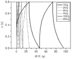
Figure 20 A, 20B and 20C for explanation be respectively included in embodiment 1 to embodiment 5 charging-the discharge curve of the electrode of the conductive laminated structure of manufacturing, according to the figure of the ratio electric capacity of current density and the ratio electric capacity under the current density of 1A/g;
Figure 21 is for showing the figure of the internal resistance of the electrode that is included in the conductive laminated structure of manufacturing in embodiment 1 to embodiment 5;
Figure 22 A and the 22B figure for showing that the Ragone of the electrode that comprises the conductive laminated structure of manufacturing in each comfortable embodiment 1 to 5 and embodiment 8-1 draws;
Figure 23 A and 23B are respectively the figure of the cyclical stability that shows the electrode that is included in the conductive laminated structure of manufacturing in embodiment 1,3,5 and embodiment 8-1;
Figure 24 is the schematic diagram of explanation biological implantation process of the ultracapacitor of the execution mode of design according to the present invention;
The schematic diagram of the method for the performance of the ultracapacitor that Figure 25 A~25C evaluates the conductive laminated structure of preparation in the embodiment 1 be included in the present invention's design for explanation in physiological environment;
The cyclic voltammetry curve of the ultracapacitor that Figure 26 A~26B shows respectively the conductive laminated structure of manufacturing in the embodiment 1 that is included in the present invention design in phosphate buffered saline (PBS) (PBS) and artificial urine (AU), and Figure 26 C be included in the conductive laminated structure manufactured in the embodiment 8-1 that the present invention conceives the cyclic voltammetry curve of ultracapacitor in mouse Skin Cell and human skin cell;
Figure 27 A and 27B are respectively the charging and discharging curve of ultracapacitor in PBS and AU that is included in embodiment 1 the conductive laminated structure of manufacturing, and Figure 27 C is the charging-discharge curve of ultracapacitor in mouse Skin Cell and human skin cell that is included in the conductive laminated structure of manufacturing in the embodiment 8-1 of the present invention's design;
Figure 28 A and 28B for show the conductive laminated structure of manufacturing in the embodiment 1 be included in the present invention's design ultracapacitor at PBS and AU in separately according to the figure of the ratio electric capacity of potential scan speed and current density, and Figure 28 C~28D for the ultracapacitor that shows the conductive laminated structure of manufacturing in the embodiment 8-1 that is included in the present invention's design mouse Skin Cell and human skin cell in separately according to the figure of the ratio electric capacity of potential scan speed and current density;
Figure 29 A, 29B, 29C and 29D for the ultracapacitor that shows respectively the conductive laminated structure of manufacturing in the embodiment 1 be included in the present invention's design in cell culture medium according to the figure of the ratio electric capacity of cyclic voltammetry curve, charging-discharge curve, cell culture medium potential scan speed and current density;
Figure 30 A and 30B are respectively the image of the cellular damage in cell culture medium with respect to charge-discharge cycles number of times of the ultracapacitor that is included in the conductive laminated structure of manufacturing in embodiment 1 and embodiment 8-1;
Figure 31 is presented in the ultracapacitor that is included in the conductive laminated structure of manufacturing in embodiment 1, embodiment 3 and embodiment 5 according to the figure of the capability retention of charge-discharge cycles number of times; With
Figure 32 A and 32B for show be included in respectively the conductive laminated structure of manufacturing in embodiment 1 and embodiment 8-1 ultracapacitor according to the figure of the stability of the ratio electric capacity of charge-discharge cycles number.
Embodiment
To conductive laminated structure, the electrode that comprises described conductive laminated structure and ultracapacitor and the method for manufacturing described conductive laminated structure be described in detail now, the example is illustrated in accompanying drawing, and wherein identical Reference numeral refers to identical element all the time.In this, present embodiment can have different forms and should not be construed as and is limited to illustrated description herein.Therefore, below only by description execution mode as shown in FIG., to explain the aspect of this description.Term "and/or" comprises one or more any and whole combination of relevant Listed Items as used herein.Statement for example " ... at least one (kind) " when before or after key element list, is modified whole key element list, rather than is modified the independent key element of described list.
The execution mode of design according to the present invention, conductive laminated structure comprises: DNA hydrogel; With polymer dielectric on described DNA hydrogel and the composite layer of electric conducting material.
Described DNA hydrogel as three-dimensional porous structure body can form by branched DNA is cross-linked.Described branched DNA can be the branched DNA of X-shape, the branched DNA of the branched DNA of gamma-form or T-shape.
By regulating initial concentration and the type of described branched DNA, can accurately control the size and shape of described DNA hydrogel.
Described DNA hydrogel can have and has several nanometers to the very thin flat or leaf layered porous structure of the thickness of hundreds of nanometers.Described DNA hydrogel can be electronegative due to the phosphate groups in DNA skeleton.
The composite layer of described polymer dielectric and electric conducting material can have the multilayer structure making that comprises 2~20 layers.Described multilayer structure making can be arranged on both sides to be symmetrical about described DNA hydrogel.In this, described composite layer can comprise the electric conducting material being evenly dispersed on described polymer dielectric.Described electric conducting material can be conducting polymer or carbon nano-tube.
When described composite layer has multilayer structure making, described electric conducting material dispersibles at least one polymer dielectric.Especially, all layers in described composite layer can comprise the electric conducting material being dispersed in polymer dielectric.In some embodiments, some layers in described composite layer can comprise the electric conducting material being dispersed in polymer dielectric, and the remainder of described layer can only comprise polymer dielectric and there is no electric conducting material.
Described DNA hydrogel and described composite layer can be bonded to each other by electrostatic attraction.Especially, described DNA hydrogel can be electronegative due to the existence of phosphate groups, and therefore,, if the described polymer dielectric in described composite layer has positive charge, described DNA hydrogel can be stably combined with the composite layer on it by electrostatic attraction.
When described composite layer has multilayer structure making, the layer in described composite layer also can combine by electrostatic attraction.; when described DNA hydrogel is electronegative; the first composite layer that comprises the polymer dielectric with positive charge can directly be attached to described DNA hydrogel by electrostatic attraction; can be arranged on described the first composite layer by electrostatic attraction with the second composite layer that comprises the polymer dielectric with negative electrical charge, make to form as the layer of positively charged and electronegative layer to replace stacking (layer-by-layer) layer by layer assembly by electrostatic attraction.
In some embodiments, when the DNA hydrogel that has large specific area and a high biocompatibility when use is manufactured described conductive laminated structure as template, because electric conducting material can be directly on described DNA hydrogel, therefore at least one polyelectrolyte floor can be placed in contact to described DNA hydrogel, wherein electric conducting material is dispersed in described at least one polyelectrolyte floor.
The quantity of described composite layer is larger, and described electric conducting material content and the conductivity of described conductive laminated structure are higher.Yet the weight of increase of multilayer structure making with the composite layer of larger amt can cause the conductivity reducing.Therefore, can control suitably the quantity of composite layer.For example, described composite layer can comprise for example 2~20 layers.
The described polymer dielectric with positive charge can be and is selected from following at least one: poly-(chlorination diallyl dimethyl ammonium) (PDADMAC), poly-(allylamine hydrochloride) (PAH), poly-(aziridine) (PEI) and poly-(dimethylaminoethyl acrylate methyl base amino-2-ethyl ester) (PDMAEMA).
The described polymer dielectric with negative electrical charge is to be selected from following at least one: poly-(sulphur styrene) (PSS), poly-(acrylic acid) (PAA), poly-(vinylsulfonate) (PVS) and poly-[1-[4-(3-carboxyl-4-hydroxyphenyl azo) benzene sulfonamido]-1,2-ethane two bases, sodium salt] (PAZO).
Described electric conducting material can be the graphene oxide of conducting polymer, carbon nano-tube or reduction.Described conducting polymer can be water dispersible.Owing to being water dispersible, described conducting polymer can dispersible in the polymer dielectric aqueous solution equably.; difficulty when directly forming conductive polymer coating on described DNA hydrogel; after forming polyelectrolyte floor by electrostatic attraction on described DNA hydrogel, conducting polymer can be dispersed on described polyelectrolyte floor, manufacture thus conductive laminated structure.
Described conducting polymer can be at least one that is selected from polyaniline, polythiophene, polypyrrole and poly-(3,4-ethylidene dioxy thiophene).
Described carbon nano-tube can be Single Walled Carbon Nanotube or multi-walled carbon nano-tubes.
When described electric conducting material is carbon nano-tube, layered structure can further be included in the polyaniline (PANI) on the described polyelectrolyte floor that comprises described carbon nano-tube.
In some embodiments, owing to having large specific area and high conductivity, described conductive laminated structure can be applicable to electrode and energy accumulating device for example in ultracapacitor, lithium ion battery or fuel cell.
Another execution mode of design according to the present invention, electrode comprises: collector; With the electrode active material being arranged on described collector, described electrode active material comprises: DNA hydrogel; Be arranged on polymer dielectric on described DNA hydrogel and the composite layer of electric conducting material.
In some embodiments, adopt porous DNA hydrogel as template, can on described porous DNA hydrogel, form the composite layer of polymer dielectric and electric conducting material to obtain the electric conducting material with very large specific area in electrode to be used in.
In described electrode, described DNA hydrogel and described composite layer can be bonded to each other by electrostatic attraction.Described composite layer can have the multilayer structure making that comprises 2~20 layers.Described multilayer structure making can be on both sides being symmetrical about described DNA hydrogel.
The described composite layer of described electrode can be the polyelectrolyte floor with positive charge and polyelectrolyte floor alternately stacking with negative electrical charge, and wherein said electric conducting material is dispersed at least one layer in described composite layer.Described electric conducting material can be conducting polymer or carbon nano-tube.When described composite layer has multilayer structure making, the layer in described composite layer also can combine by electrostatic attraction.
In some embodiments, when ultracapacitor that described electrode for example can be implanted for ultracapacitor, described collector can be biocompatible collector.
In some embodiments, the described biocompatible collector of described electrode can comprise at least one metal that is selected from Au, Ag, Pt, Ti and Fe.
In some embodiments, the described electrode for the ultracapacitor that can implant can be used the manufacture of DNA hydrogel, and therefore can be biocompatible and can implant.
According to the present invention design another execution mode, ultracapacitor comprise negative electrode, anode and be arranged on described negative electrode and described anode between electrolyte, at least one of described negative electrode and described anode is above-mentioned electrode.
In some embodiments, described ultracapacitor can further comprise dividing plate.The described negative electrode of described ultracapacitor can be the above-mentioned electrode of the design according to the present invention.The described anode of described ultracapacitor can be identical or different with described negative electrode.Described anode can be any anode as known in the art.
Fig. 1 is the schematic diagram of the ultracapacitor 100 of the execution mode of design according to the present invention.
As shown in fig. 1, ultracapacitor 100 comprise have the first collector 10a and the first active layer 20a the first electrode 110a, dividing plate 30, there is the second electrode 110b of the second collector 10b and the second active layer 20b and fill the first active layer 20a and the electrolyte (not shown) of the second active layer 20b.The first electrode 110a and the second electrode 110b can be symmetrical about dividing plate 30, and can aspect structure and characteristics, be identical.Hereinafter, only the first electrode 110a will be described in more detail.Can the description as the second electrode 110b with reference to the following description of the first electrode 110a.
The first electrode 110a can comprise the first collector 10a and the first active layer 20a.The first collector 10a can collect electronics or can be to the first active layer 20a supplies electrons from the first active layer 20a.The first collector 10a can by the metal with high conductivity for example aluminium, nickel, copper or titanium form, but be not limited to this.The first collector 10a can collect electronics or can be to the first active layer 20a supplies electrons from the first active layer 20a, and can be biocompatible.The first collector 10a can by the metal of high conductivity for example gold, silver, platinum, titanium or iron form, but be not limited to this.
The first active layer 20a can be arranged on the first collector 10a.The first active layer 20a can comprise DNA hydrogel and be arranged on polymer dielectric on described DNA hydrogel and the composite layer of electric conducting material.
When being filled with electrolytical the first active layer 20a and applying voltage, described electrolyte is separated into cation and anion.The cation of described electrolytical separation and anion can move to form electric double layer to the first electrode 110a and the second electrode 110b respectively.
If the first electrode 110a of the ultracapacitor with electric double layer 100 of Fig. 1 and the second electrode 110b are launched in the plane, the first electrode 110a and the second electrode 110b can be assumed to the electrode being set parallel to each other of ordinary capacitor.Therefore, can use the electrostatic capacitor (charging capacitor, charge capacitance) of the ultracapacitor with electric double layer 100 of equation 1 definite Fig. 1 below.
[equation 1]
Wherein C is electric capacity, the dielectric constant that ε is electrode material, the specific area that A is electrode, and the d thickness that is electric double layer.The thickness of electric double layer (d) can be about 0.2nm~about 1nm.The specific area of electrode (A) refers to the contact area of electrode and electrolyte ion.In determining these factors of electrostatic capacitor (C), the thickness (d) of the dielectric constant of electrode material (ε) and electric double layer is conditional.Therefore, the specific area of control electrode (A) is effective for high electric capacity.
In some embodiments, the specific area that described ultracapacitor can be large and have high electric capacity, because after the formation of the composite layer of sandwich construction, the loose structure of described DNA hydrogel can keep.
In some embodiments, described ultracapacitor can be the ultracapacitor that can implant that there is no cytotoxicity and stably can move on cell in physiological environment.Described ultracapacitor can be can be implanted in human organ.
In addition,, because the physical absorption by ion and desorb store and utilize the ability of energy, even after reruning in physiological environment, described ultracapacitor can almost not have toxicity yet.Therefore, described ultracapacitor can be used as the biocompatible energy accumulating device enforcement that can implant in human organ.
Electrolyte between described negative electrode and described anode can be the liquid form being dissolved in solvent.Described electrolytical solvent can be at least one that is selected from acetonitrile, dimethyl ketone and propylene carbonate.Described electrolyte can have the solubility of approximately 0.01 mole/L in described solvent, and it is inactive within the scope of the working voltage of described ultracapacitor, to can be electricity.
Described electrolyte can be H
2sO
4, Na
2sO
4, Li
2sO
4, LiPF
6, lithium perchlorate, LiBF4, KCl, KOH and two (trifyl) imines (EMIM/TFSI) of 1-ethyl-3-methylimidazole at least one.
Dividing plate 30 can be divided into negative electrode and anode by the inner space of described ultracapacitor, and prevents the electrical short between described negative electrode and described anode.Dividing plate 30 can be formed by for example polypropylene, polyethylene or Teflon, but is not limited to this.
In some embodiments, described ultracapacitor can be and comprises the following ultracapacitor that can implant: negative electrode, anode and be arranged on described negative electrode and described anode between biocompatible dividing plate, at least one of described negative electrode and described anode is the above-mentioned electrode that can implant.
Described biocompatible dividing plate can be divided into negative electrode and anode by the inner space of described ultracapacitor, and prevents the electrical short between described negative electrode and described anode.Described biocompatible dividing plate can be formed by for example polypropylene, polyethylene, Teflon, cellulose or hydrogel, but is not limited to this.
In some embodiments, the described dividing plate that can implant can be and for example can implant in bladder or eyeball at human organ.
In some other execution modes, the described dividing plate that can implant can further comprise that the described negative electrode of covering, described anode and described biocompatible dividing plate be not to be subject to the isolated protective layer of adjacent ambient.
Described isolated protective layer can comprise the biocompatible material that is selected from cellulose, hydrogel and combination thereof.
Described isolated protective layer can have the thickness of approximately 1 μ m~approximately 1000 μ m.
In some execution modes of the described ultracapacitor that can implant, different with the electrolyte of common ultracapacitor, the ion in the biofluid of the described ultracapacitor implantation that can implant human organ wherein can play electrolytical effect.When applying voltage from external power supply to human organ, comprise that ion in the biofluid of described human organ of described ultracapacitor is to the negative electrode of the ultracapacitor of implanting and the electric double layer that anode moves to be formed for charging and discharging.
Another execution mode of design according to the present invention, the method for manufacturing conductive laminated structure comprises: preparation DNA hydrogel; Described DNA hydrogel is immersed in the first polymer dielectric solution with the polarity contrary with described DNA hydrogel; The described DNA hydrogel with described the first polymer dielectric solution is dry to form the first polyelectrolyte floor on described DNA hydrogel; With the described DNA hydrogel with described the first polyelectrolyte floor is immersed in the second polymer dielectric solution with the polarity contrary with described the first polyelectrolyte floor; On the DNA hydrogel with described the first polyelectrolyte floor through dipping is dried with described the first polyelectrolyte floor on described DNA hydrogel, form the second polyelectrolyte floor, wherein said the second polyelectrolyte floor can be wherein electric conducting material and is dispersed in the composite layer in the second polymer dielectric.
Fig. 2 A is the schematic diagram of explanation manufacture process of the conductive laminated structure of an execution mode of design according to the present invention, and the manufacture process of Fig. 2 B explanation conductive laminated structure of another execution mode of design according to the present invention.
In some embodiments, described method can further comprise: by the DNA hydrogel that there is the first polyelectrolyte floor and for example comprise the layer of PDADMAC be immersed in there is the polarity contrary with described the first polyelectrolyte floor forming on described DNA hydrogel wherein dissolve the second polymer dielectric for example in the solution of PEDOT:PSS; With to have on the described DNA hydrogel of described the first polyelectrolyte floor, form the second polyelectrolyte floor by the DNA hydrogel that comprises described the first polyelectrolyte floor through dipping is dry.
Another execution mode of design according to the present invention, described method can comprise by the DNA hydrogel that there is the first polyelectrolyte floor and for example comprise the layer of PDADMAC be immersed in have the polarity contrary with described the first polyelectrolyte floor forming on described DNA hydrogel wherein dispersed electro-conductive material comprise that the second polymer dielectric is for example in the solution of SWCNT:PAH; With form the second polyelectrolyte floor on described the first dielectric substrate on described DNA hydrogel by the DNA hydrogel with described the first polyelectrolyte floor through dipping is dry.Here, when the described electric conducting material comprising when described the second polyelectrolyte floor is SWCNT, can on described the second polyelectrolyte floor, form PANI layer.
According to the present invention, another execution mode of design, is immersed in the DNA hydrogel with described the second polyelectrolyte floor in the terpolymer electrolyte solution with the polarity contrary with described the second polyelectrolyte floor; With form terpolymer dielectric substrate on described the second polyelectrolyte floor on described DNA hydrogel and can repeat to form other polyelectrolyte floor the DNA hydrogel with described the second polyelectrolyte floor through dipping is dry, one or more layers of wherein said terpolymer dielectric substrate and described other polyelectrolyte floor can be wherein electric conducting material and are dispersed in the composite layer in polymer dielectric.
The multiple polymers electrolyte that described terpolymer dielectric substrate and described other polyelectrolyte floor comprise can be same to each other or different to each other.
Described DNA hydrogel can be by being prepared as follows: the hybridization by single stranded DNA obtains branched DNA, and make described branched DNA crosslinked.
Can design and synthesize described branched DNA to there is the arm that has complementary cohesive end.The length of each arm of adjustable described branched DNA.Described branched DNA can be used T4 ligase crosslinked together to form the DNA hydrogel (also referred to as DNA gel or Dgel) with three-dimensional structure.The method of preparing DNA hydrogel is disclosed in document (Letters, 2006.9.24.pp797-801, Enzyme-catalysed assembly of DNA hydrogel), by it by reference in being incorporated herein.
Described branched DNA can be the branched DNA of X-shape, the branched DNA of the branched DNA of gamma-form or T-shape.
Described DNA hydrogel can be immersed in polymer dielectric solution described polymer dielectric is attached on described DNA hydrogel by electrostatic attraction.For example, when described DNA hydrogel has negative electrical charge, described DNA hydrogel can be immersed in the polymer dielectric solution with positive charge described polymer dielectric is attached on described DNA hydrogel by electrostatic attraction.
Described dipping can be undertaken by immersion, washing and freeze drying.For example, described dipping can use known polymer layer by layer (LBL) method carry out.
After described polymer dielectric solution shifts out, can the described DNA hydrogel of being combined with described polymer dielectric is dry to form described polyelectrolyte floor on described DNA hydrogel.
Described method can be included in described dry washing before.Described washing can reduce to be combined in the thickness of the described polyelectrolyte floor on described DNA hydrogel.The described DNA hydrogel that for example, can use distilled water washing to be combined with described polymer dielectric.
Described electric conducting material can be conducting polymer and can in described polymer dielectric solution, have high dispersiveness.Described electric conducting material can be water dispersible.Described conducting polymer can be at least one of polyaniline, polythiophene, polypyrrole and poly-(3,4-ethylidene dioxy thiophene).
Carbon nano-tube can be used as described electric conducting material.Single Walled Carbon Nanotube or multi-walled carbon nano-tubes can be used as described carbon nano-tube.
Described dry can being undertaken by freeze drying.Described freeze drying can be carried out approximately 12 hours~approximately 24 hours at the temperature of approximately-60 ℃~approximately-80 ℃.Described freeze drying can prevent from comprising that the layered structure of the described composite layer of described DNA hydrogel and described polymer dielectric and electric conducting material is compromised.
The concentration of described polymer dielectric solution can be about 10mM~about 100mM, and the amount of the described conducting polymer using can be approximately 0.5 % by weight~approximately 2.0 % by weight.
As described conducting polymer, be scattered in described polymer dielectric solution wherein, can use the 1 % by weight PEDOT/PSS solution being available commercially.
When using carbon nano-tube as electric conducting material, PAH can be used as polymer dielectric.
Can make carbon nano-tube electronegative to improve the dispersiveness of described carbon nano-tube in polymer dielectric.Can use any electronegative method of carbon nano-tube that makes, for example, can use the dispersant method that for example SDBS and PAA mix with Single Walled Carbon Nanotube.Here, the relative quantity of use can be for example CNT:SDBS=1:2 (weight: weight).
On the other hand, when using carbon nano-tube as electric conducting material, can use PANI to pass through faraday (Faradaic) reaction and improve electric capacity.
PANI is one of fake capacitance material and is polymer, and therefore can carry out solution process, with other inorganic fake capacitance material MnO for example
2and RuO
2on the contrary.In addition, PANI can be according to pH and positively charged, and therefore, for can be used on the conducting polymer in LBL process.Can use the PANI solution of about 5mg/ml~about 40mg/ml to form PANI layer.
When the thickness of described PANI layer is too thick, the conductivity of layered structure can reduce due to the low conductivity of described PANI itself.
On the other hand, internal resistance can be according to the pH during the manufacture process of solution that comprises described PANI and difference, and therefore, described pH is lower, and the internal resistance of described PANI is lower, and described pH can be approximately 1.0~approximately 2.0.
When manufacturing described conductive laminated structure, the pH of adjustable described polymer dielectric solution to be to be controlled at the amount of the electric charge in described polymer dielectric, the combination between promoting layer thus.
Can be recycled and reused for the step that forms described polyelectrolyte floor on described DNA hydrogel to form the multilayer structure making of the composite layer that comprises one or more polymer dielectrics that comprise electric conducting material on described DNA hydrogel.
For example, the DNA hydrogel with the polyelectrolyte floor of positively charged can be immersed in the solution that comprises electronegative polymer dielectric and electric conducting material, then dry, to form the polyelectrolyte floor of wherein said positively charged and the composite layer of described electronegative polymer dielectric and described electric conducting material is sequentially formed at the conductive laminated structure on described DNA hydrogel.Can repeat these processes to obtain the conductive laminated structure with the expection number of plies.Used hereinly comprise that the solution of polymer dielectric can comprise identical or different polymer dielectric, and can comprise or can not comprise electric conducting material.
When described composite layer has multilayer structure making, described composite layer can be arranged on both sides to be symmetrical about described DNA hydrogel.
In all or some layers that described electric conducting material can be in the described multi-layer composite materials bed of material.
The described polymer dielectric with positive charge can be selected from poly-(chlorination diallyl dimethyl ammonium) (PDADMAC), poly-(allylamine hydrochloride) (PAH), poly-(aziridine) (PEI) and poly-(dimethylaminoethyl acrylate methyl base amino-2-ethyl ester) (PDMAEMA) at least one.
The described polymer dielectric with negative electrical charge can be selected from poly-(sulphur styrene) (PSS), poly-(acrylic acid) (PAA), poly-(vinylsulfonate) (PVS) and poly-[1-[4-(3-carboxyl-4-hydroxyphenyl azo) benzene sulfonamido]-1,2-ethane two bases, sodium salt] (PAZO) at least one.
In some execution modes of method of manufacturing conductive laminated structure, use has the DNA hydrogel of large specific area as template, pass through shape-preserving coating, for example use layer assembly method, electric conducting material can be coated on described DNA hydrogel, to form the conductive laminated structure with large specific area.By simple dip-coating and dry run, can obtain and there is the conductive laminated structure of conductive coating highly uniformly.
Comprise that the described conductive laminated structure of the described composite layer of described DNA hydrogel and the described polymer dielectric on described DNA hydrogel and described electric conducting material can be used as the electrode active material of the electrode for implanting.For example, the electrode that can implant can be used described electrode active material to be for example manufactured by the following according to common electrode manufacturing method: the slurry of preparing described electrode active material, described slurry is coated on biocompatible collector, and by products therefrom freeze drying.
Another execution mode of design according to the present invention, in body electronic installation comprise according to the present invention design the conductive laminated structure of above-mentioned one or more execution modes.The described conductive laminated structure that use utilizes DNA hydrogel to manufacture as template, in described body electronic installation multiple human organ arbitrarily in muscle cell, be for example biocompatible and can implant.
Hereinafter, with reference to the following example, describe one or more execution mode of the present invention in detail.Yet these embodiment are not intended to limit the scope of described one or more execution modes of the present invention.
preparation Example 1
the preparation of DNA hydrogel
By single stranded DNA (being provided by Bioneer) hybridization being obtained to the branched DNA of X-shape, wherein the T4DNA ligase for monomer (Promega) of the X-shape of 10nmol is hybridized 12 hours at 16 ℃.The length of each arm is about 6nm.The branched DNA of described X-shape is mixed with the T4-ligase of 6 units, and at approximately 16 ℃ stir about 12 hours to obtain DNA hydrogel.Fig. 3 A and 3B are respectively scanning electron microscopy (SEM) image of described DNA hydrogel under * 60 and * 300 enlargement ratio.
As shown in Figure 3A and 3B, described DNA hydrogel has and has several nanometers to the very thin flat or leaf layered porous structure of the thickness of hundreds of nanometers.Described DNA hydrogel is because the phosphate groups in DNA skeleton has negative electrical charge.
the manufacture of conductive laminated structure
The DNA hydrogel of preparation in Preparation Example 1 is at room temperature immersed as poly-(the chlorination diallyl dimethyl ammonium) with 100000~200000 molecular weight of the polymer of positively charged (PDADMAC) in (Aldrich) aqueous solution (20mM) approximately 30 minutes.Afterwards, described DNA hydrogel is shifted out from described solution, with distilled water washing, then at approximately-80 ℃ freeze drying approximately 12 hours to there is the PDADMAC layer being deposited thereon.The DNA hydrogel with described PDADMAC layer is at room temperature immersed as poly-(the sulphur styrene) of electronegative polymer (PSS) in the aqueous solution of (1 % by weight) (poly-(3,4-ethylidene dioxy thiophene) (PEDOT) (Heraeus) is dispersed in the described aqueous solution) approximately 30 minutes.Afterwards, described DNA hydrogel is shifted out from described solution, with distilled water washing, then at approximately-80 ℃ freeze drying approximately 12 hours to obtain the stacked structure body of the composite layer with the PDADMAC layer/PEDOT-PSS layer in the opposed surface of described DNA hydrogel.
The image of the result that Fig. 4 explanation is drawn as energy dispersion spectrometry (EDS).As shown in Figure 4, the lobate region of finding described DNA hydrogel is coated with equally distributed conductive PEDOT equably.Fig. 5 illustrates the Raman spectrum of above-mentioned stacked structure body.As shown in Figure 5, find that described electric conducting material PEDOT is visual visible.
The stacked structure body of embodiment 1 is at room temperature immersed in the aqueous solution of the PDADMAC (20mM) of the polymer of positively charged approximately 30 minutes.Afterwards, DNA hydrogel is shifted out from described solution, with distilled water washing, then at approximately-80 ℃ freeze drying approximately 12 hours to form the composite layer of PDADMAC layer/PEDOT-PSS layer/PDADMAC layer on described DNA hydrogel.
Described stacked structure body is at room temperature immersed in the aqueous solution (PEDOT is dispersed in the described aqueous solution) of the PSS (1 % by weight) as electronegative polymer approximately 30 minutes.Afterwards, described DNA hydrogel is shifted out from described solution, with distilled water washing, then at approximately-80 ℃ freeze drying approximately 12 hours to obtain the stacked structure body of the composite layer with the PDADMAC layer/PEDOT-PSS layer/PDADMAC layer/PEDOT-PSS layer in the opposed surface of described DNA hydrogel.
On the stacked structure body of embodiment 2, repeat process in the same manner as in Example 2 to form the stacked structure body of the composite layer with the PDADMAC layer/PEDOT-PSS layer/PDADMAC layer/PEDOT-PSS layer/PDADMAC layer/PEDOT-PSS layer in the opposed surface of described DNA hydrogel.
On the stacked structure body of embodiment 3, repeat process in the same manner as in Example 3 to form the stacked structure body of the composite layer with the PDADMAC layer/PEDOT-PSS layer/PDADMAC layer/PEDOT-PSS layer/PDADMAC layer/PEDOT-PSS layer/PDADMAC layer/PEDOT-PSS layer in the opposed surface of described DNA hydrogel.
On the stacked structure body of embodiment 4, repeat process in the same manner as in Example 4 to form the stacked structure body of the composite layer with the PDADMAC layer/PEDOT-PSS layer/PDADMAC layer/PEDOT-PSS layer/PDADMAC layer/PEDOT-PSS layer/PDADMAC layer/PEDOT-PSS layer/PDADMAC layer/PEDOT-PSS layer in the opposed surface of described DNA hydrogel.
Fig. 6 A~6E is the SEM image of the conductive laminated structure of embodiment 1 to 5, and the metamorphosis for the number of plies is described in described conductive laminated structure.
As shown in Fig. 6 A~6E, overall layered porous structure keeps constant, does not rely on the quantity of the composite layer that comprises conducting polymer and polymer dielectric.This is owing to the very thin thickness of each layer.There is no the constant cell structure that reduce in hole is very important for keeping larger specific area.
preparation Example 2
preparation SDBS-SWCNT
15mg SWCNT (Iljin CNT) is added in SDBS (Aldrich, 30mg), and then sonication is dispersed in the SWCNT in electronegative electrolyte to obtain.
Fig. 7 A for TEM image and Fig. 7 B after in SWCNT is dispersed in to SDBS be the enlarged image of Fig. 7 A.As shown in Figure 7A and 7B, SDBS is attached to SWCNT equably and up hill and dale.Fig. 7 C is the SEM image after SDBS combination.As shown in Fig. 7 C, the diameter of the CNT bundle that susceptible of proof disperses is substantially uniformly generally.
preparation Example 3
preparation PAA-SWCNT
15mg CNT is dispersed in 3ml200mg/ml PAA (can the derive from Aldrich) aqueous solution and is dispersed in the SWCNT in electronegative electrolyte with preparation.
Fig. 8 A and 8B are TEM image before Single Walled Carbon Nanotube is attached to PAA and afterwards.As shown in Figure 8A and 8B, susceptible of proof PAA is attached to SWCNT equably and up hill and dale.Fig. 8 C is at the SEM image in conjunction with after PAA.As shown in Fig. 8 C, the diameter of the CNT bundle that susceptible of proof disperses is substantially uniformly generally.
Meanwhile, by using acoustic processing method to measure the ξ electromotive force that is dispersed in the SWCNT in electronegative electrolyte being obtained by Preparation Example 2 and Preparation Example 3, and the results are shown in following table 1.
[table 1]
| ? | ξ electromotive force (mV) |
| Preparation Example 2 | -44.04±4.51 |
| Preparation Example 3 | -48.93±5.73 |
As above shown in table 1, SWCNT is electronegative.
The DNA hydrogel of preparation in above Preparation Example 1 is at room temperature immersed to poly-(allylamine hydrochloride) (PAH) in (Aldrich) aqueous solution (concentration of 20mM) (its polymer that is positively charged) 30 minutes with 70,000 molecular weight.Then, described DNA hydrogel is taken out, with distilled water washing, and freeze drying 12 hours at the temperature of-80 ℃.Subsequently, the stacked DNA hydrogel of PAH is at room temperature immersed in Preparation Example 2 in the SDBS-SWCNT aqueous solution (concentration of 0.25 % by weight) of preparation to 30 minutes.Then, described DNA hydrogel is taken out, with distilled water washing, and at the temperature of-80 ℃ freeze drying 12 hours to form the layered structure of the composite layer with the PAH layer/SDBS-SWCNT layer on the both sides of described DNA hydrogel.
Fig. 9 A~9C is that the SEM image, its SEM image that amplifies 300 times of the layered structure of above preparation and its amplify the SEM image of 50000 times.As shown in Fig. 9 A~9C, susceptible of proof composite layer evenly and is smoothly formed on DNA hydrogel.
The DNA hydrogel of preparation in Preparation Example 1 is at room temperature immersed to poly-(allylamine hydrochloride) (PAH) in the aqueous solution (concentration of 20mM) (it is the polymer of positively charged) 30 minutes.Then, described DNA hydrogel is taken out, with distilled water washing, and freeze drying 12 hours at the temperature of-80 ℃.Subsequently, the stacked DNA hydrogel of PAH is at room temperature immersed in Preparation Example 3 in the PAA-SWCNT aqueous solution (concentration of 1 % by weight) of preparation to 30 minutes.Then, described DNA hydrogel is taken out, with distilled water washing, and at the temperature of-80 ℃ freeze drying 12 hours to form the layered structure of the composite layer with the PAH layer/PAA-SWCNT layer on the both sides of described DNA hydrogel.
Figure 10 A~10C is that the SEM image, its SEM image that amplifies 300 times of the layered structure of above preparation and its amplify the SEM image of 50000 times.As shown in Figure 10 A~10C, susceptible of proof composite layer evenly and is smoothly formed on DNA hydrogel.
By using 4-point probe method to measure the sheet resistance of the layered structure of preparation in embodiment 6 and 7, and the results are shown in following table 2.
[table 2]
| ? | Sheet resistance (ohm-sq (ohm/sq)) |
| |
20.0±3.5 |
| |
15.0±3.1 |
As shown in table 2, owing to forming the conducing composite material layer that comprises electric conducting material on DNA hydrogel, therefore to compare with the sheet resistance of DNA hydrogel self, its sheet resistance significantly reduces.
preparation Example 4-1 to 4-4
preparation PANI
By water-soluble PANI (purchased from: Polysciences) be dissolved in deionized water, simultaneously by using HCl that the pH of described solution is adjusted to 1.0,2.7,4.0 and 6.0 with the preparation PANI aqueous solution.
evaluation Example 1: the evaluation of the character of the PANI preparing by use diverse ways
The PANI aqueous solution of preparing in embodiment 4-1 to 4-4 according to the electric current of voltage, be shown in Figure 11 A~11C together with the water-insoluble PANI of thing in contrast according to the conductivity of pH and Raman spectrum.As described as shown in FIG, the conductivity of water-soluble PANI depends on pH and different and have a good conductivity than water-insoluble PANI (tester).Between water-soluble PANI and water-insoluble PANI, optical property is also different.
In addition, by using constant current method to measure the electrochemistry resistance of the wet PANI preparing in Preparation Example 4-1 to 4-4.As shown in Figure 12, for the PANI aqueous solution of preparing under low pH, internal resistance is low, and therefore, under acid condition, internal resistance is low.Internal resistance is measured by the value (R=Δ IR/I) of the IR voltage drop under constant current is measured.
Embodiment 8-1 to 8-4
It is in the PANI aqueous solution of PANI of 5mg/ml, 10mg/ml, 20mg/ml and 40mg/ml 30 minutes that the layered structure of composite layer of the PAH layer/PAA-SWCNT layer on the both sides that are included in DNA hydrogel of preparation in embodiment 7 is at room temperature immersed to the concentration that comprises being obtained by embodiment 4-1.Afterwards, described DNA hydrogel is taken out and with distilled water washing, and at the temperature of-80 ℃ freeze drying 12 hours to prepare the composite layer of PAH layer/PAA-SWCNT layer/PANI layer on described DNA hydrogel.
Each SEM image that Figure 13 A~13D is the layered structure manufactured in embodiment 8-1 to 8-4.As described as shown in FIG, do not compare with there is no the embodiment 7 of described PANI, when PANI exists, the surface texture of described DNA hydrogel changes owing to applying described PANI layer; And therefore, the concentration of PANI is larger described in deducibility, and the amount of coated PANI is larger.
evaluation Example 2: cyclic voltammetry test
Use the conductive laminated structure of embodiment 1, embodiment 7 and embodiment 8-1 to 8-4 to manufacture electrode.Use cyclic voltammetry measurement curent change for change in voltage in described electrode.The results are shown in Figure 14 A and 14B.
Be used as embodiment 1, the embodiment 7 of work electrode and the conductive laminated structure of embodiment 8-1 to 8-4, as the platinum guaze sheet to electrode and as the carbon plate of collector and as the Whatman paper of dividing plate, with as electrolytical 1.0M sulfuric acid solution (H
2sO
4).Cyclic voltammetry test is used AUTOLAB PGSTAT100 potentiostat to carry out.
As shown in Figure 14 A, even if sweep speed improves, it is symmetrical that curve also keeps, and demonstrates desirable capacitor behavior.
Figure 14 B shows by change the cyclic voltammetry curve of the concentration of PANI under the sweep speed of 25mV/s, and deducibility, and compares when PANI does not exist, increases, and along with the concentration of PANI increases, than electric capacity, increases, then reduction when PANI exists than electric capacity.
evaluation Example 3: constant current charge/discharge test
Using embodiment 1 conductive laminated structure as work electrode, platinum guaze sheet as to electrode and 1.0M sulfuric acid solution as electrolyte, use AUTOLAB PGSTAT100 potentiostat under the current density of about 1A/g, to carry out constant current charge/discharge test.To the results are shown in Figure 15 A of the constant current charge/discharge test of the conductive laminated structure of embodiment 1.
The conductive laminated structure of embodiment 1 and embodiment 8-1 is immersed in phosphate buffered saline (PBS) (PBS) and artificial urine (AU) as work electrode respectively, and by using AUTOLAB PGSTAT100 potentiostat to carry out constant current charge/discharge test under the current density of about 1A/g~about 20A/g.
Figure 15 A and 15B for show comprise the conductive laminated structure of preparing in each comfortable embodiment 1 and embodiment 8-1 electrode according to the figure of the change in voltage of time.
Figure 16 for show be included in the conductive laminated structure of manufacturing in embodiment 1 electrode according to the figure of the ratio electric capacity of sweep speed.Figure 17 A and 17B for show comprise the laminated structure of manufacturing in each comfortable embodiment 1 and embodiment 8-1 electrode according to the figure of the ratio electric capacity of current density.As shown in Figure 16 and 17A, along with sweep speed and current density increase, than electric capacity, from about 40F/g, be reduced to about 5F/g.This is that the general trend of ultracapacitor and the reduction of such ratio electric capacity are attributable to the following fact: from the ion of electrolyte separation, fail to be issued to balance to form electric double layer (EDL) at porous polymer electrolyte-DNA hydrogel electrode in high sweep speed and high current density.In addition, as shown in Figure 17 B, than electric capacity, according to the increase of current density, reduce and be converged in certain value place.
Figure 18 A and 18B are for showing the figure of the cyclic voltammetry of electrode under the sweep speed of 25mV/s be included in the conductive laminated structure of preparing in embodiment 1 to 5 and embodiment 8-1.Figure 19 A for show be included in the conductive laminated structure of preparation in embodiment 1 to 5 electrode according to the figure of the ratio electric capacity of sweep speed.Figure 19 B is for showing the figure of the ratio electric capacity of electrode under the sweep speed of 25mV/s be included in the conductive laminated structure of preparation in embodiment 1 to 5.
As shown in Figure 18 A, than electric capacity, according to the quantity of stacked conducting polymer dielectric substrate, increase linearly; Yet specific capacity does not increase and exceeds certain value, this may be because the increase of the electric capacity causing due to the increase of surface area cancels each other out with the reduction of the electric capacity causing due to weight increase.
As shown in Figure 18 B, when using the electrode applying through PANI, at acidic electrolyte bath (H
2sO
4) in ratio capacity ratio at neutral electrolyte (Na
2sO
4) in increase manyly because the conductivity of PANI depends on the pH of solution.
As shown in Figure 19 A, can be observed, therein in the situation of the electrode of stacked a plurality of conducting polymers, than electric capacity along with sweep speed increases and reduces, because depend on potential scan speed than electric capacity.
As shown in Figure 19 B, along with the quantity increase of composite layer, the ratio electric capacity (Csp) under identical sweep speed increases.The composite layer that adopts three or larger quantity, no longer increases than electric capacity (Csp).Under the sweep speed of about 25mV/s, than electric capacity (Csp), increase until about 57.7F/g.
Figure 20 A be included in embodiment 1 to 5 preparation the electrode of conductive laminated structure under the current density of about 1A/g for the figure of the cyclic voltammetry of time.Figure 20 B is the figure of ratio electric capacity of the variation for current density of electrode that is included in embodiment 1 to 5 the conductive laminated structure of preparation, and Figure 20 C is the figure of the ratio electric capacity of electrode under the current density of about 1A/g that is included in the conductive laminated structure of preparation in embodiment 1 to 5.
As shown in Figure 20 C, adopt three layers or more multi-layered, than electric capacity (Csp), no longer increase, and under the current density of 1A/g, than electric capacity, be increased to about 58.3F/g.This is owing to the following fact: along with the quantity of composite layer increases, due to the PEDOT layer of larger quantity, conductivity increases.
Figure 21 is the figure of the internal resistance of the electrode of demonstration embodiment 1 to 5.Figure 22 A and 22B are that the Ragone that is included in the electrode of the conductive laminated structure of preparing in embodiment 1 to 5 and embodiment 8-1 draws.Figure 23 A and 23B are for showing the figure of the cyclical stability of electrode under the current density of about 2A/g be included in the conductive laminated structure of preparing in embodiment 1,3,5 and embodiment 8-1.
As shown in Figure 21, in the electrode of Preparation Example 5 that comprises 5 composite layers, electrochemistry internal resistance is lower by approximately 37% than comprising in the electrode of a composite layer.In having the structure of 3 or more layer, do not observe than the remarkable increase of electric capacity (Csp), the reduction of the ratio electric capacity (Csp) that the increase of the ratio electric capacity (Csp) that this causes owing to the internal resistance owing to reducing is caused by the quality of the increase due to electrode active material is offset.As shown in the Ragone drawing of Figure 22 A, along with the quantity increase of composite layer, power density and current density increase, and this shows to compare with business ultracapacitor (frame of being demarcated by solid line) similar or better a little performance.As shown in Figure 22 B, known CNT therein and PANI are layered in the situation of the electrode on DNA hydrogel, and Performance Ratio business ultracapacitor is much better.
In addition,, as shown in Figure 23 A and 23B, carry out loop test to determine charge/discharge stability.As a result, until approximately 200 circulations, than electric capacity (Csp), keep almost constant and do not reduce.That is, even after charge/discharge cycle repeatedly, also can keep and the similar capacitance of initial level than electric capacity.Yet, after approximately 200 times or more times circulation, there is performance degradation gradually.After approximately 1000 circulations, in thering is the structure of 3 to 5 composite layers, than electric capacity (Csp), reach the approximately 82%-84% of initial Csp, and in thering is the structure of a composite layer, than electric capacity (Csp), remain on approximately 65% of initial Csp.Than these of electric capacity, reduce owing to the metamorphosis in stacked structure body (mechanical failure) being caused by the desorb of conductive PEDOT and the sorption and desorption of electrolyte ion during charge/discharge.In having the layered structure of 3 to 5 composite layers, polymer dielectric packaging effect in PEDOT layer is comparable strong in the stacked structure body of one deck, and therefore porous electrode can become and more tolerates the distortion being caused by charge/discharge.
The electrode that comprises conductive coating structure body of embodiment 1 has about 50F/g or higher high specific capacitance, about 5000W/kg or higher power density and about 1Wh/kg or higher energy density.
embodiment 9
the manufacture of ultracapacitor
Use drippage curtain coating (drop casting) and freeze drying on two goldleaf as collector, to apply respectively the stacked structure body of embodiment 5, subsequently the cellulose paper as dividing plate is inserted on two relative its and has between the stacked structure body of metal forming, and with polymer pouches sealing, manufacture thus the ultracapacitor that can implant as embodiments of the present invention illustrating in Figure 24.
In physiological environment, measure the performance of the described ultracapacitor that can implant., the described ultracapacitor that can implant is immersed in phosphate buffered saline (PBS) (PBS), artificial urine (AU) and cell culture medium, as illustrated with measurement performance in Figure 25 A~25C for this reason.In Figure 25 A~25C, " sample " represents the layered structure as the embodiment 5 of the composite layer that comprises DNA hydrogel and polymer dielectric and electric conducting material of electrode active material.Described PBS has pH7.4 (can derive from Gibco).Described artificial urine (AU) comprises 1.1mM lactic acid, 2.0mM citric acid, 2.5mM sodium carbonate, 2.5mM calcium chloride, 90mM sodium chloride, 2.0mM magnesium sulfate, 10mM sodium sulphate, 7.0mM potassium dihydrogen phosphate, 7.0mM dipotassium hydrogen phosphate, 25mM ammonium chloride and 170mM urea.Described cell culture medium comprises MEM (Minimum Essential Medium with Earle'sBalanced the Salts) (MEM/EBSS with E Ershi balanced salt, comprise NIH3T3 cell and monkey Skin Cell), the improved Eagle culture medium of Dulbecco (DMEM, comprise HDF cell, human skin cell), 10% hyclone and 1% penicillin.
Figure 26 A and 26B are presented at respectively the result (arriving under the different potential scan speed of about 2000mV/s at about 25mV/s) of the constant current charge/discharge test in PBS and AU.Figure 26 C shows the cyclic voltammetry curve when using NIH3T3 and HDF cell culture medium as electrolyte.As shown in Figure 26 A and 26B, even if adopt the sweep speed increasing, it is symmetrical that described curve also keeps, and demonstrates desirable capacitor behavior.In addition,, as shown in Figure 26 C, knownly in cell culture medium, demonstrate identical effect.Figure 27 A and 27B are used respectively the result of the constant current charge/discharge test of described ultracapacitor for what measure according to above-mentioned method in PBS and AU.As shown in Figure 27 A and 27B, described ultracapacitor is operation reposefully in PBS and AU.Figure 27 C demonstration use NIH3T3 and HDF cell culture medium are as the result of electrolytical constant current charge/discharge test.As shown in Figure 27 C, described ultracapacitor is in the operation reposefully in both of different cell culture mediums.
The ratio electric capacity that Figure 28 A~28C is the function as potential scan speed that obtained by cyclic voltammetry and by the figure of the ratio electric capacity of the function as current density of charge/discharge data acquisition.As shown in Figure 28 A~28C, discovery is as the ultracapacitor that is included in the conductive laminated structure of manufacturing in embodiment 1 operation reposefully in PBS and AU of embodiment of the present invention, and under different potential scan speed and current density, in AU than in PBS, there is the ratio electric capacity of approximately 2.5 times high.
In cell culture medium, test is as cytotoxicity and the chemical property of the ultracapacitor of embodiments of the present invention.
In cell culture medium, the ultracapacitor that is included in the conductive laminated structure of manufacturing in embodiment 1 as embodiments of the present invention is carried out to cyclic voltammetry test and charge/discharge test in the same manner as described above.The results are shown in Figure 29 A and 29B.The ratio electric capacity that Figure 29 C and 29D are the function as potential scan speed that obtained by cyclic voltammetry and by the figure of the ratio electric capacity of the function as current density of charge/discharge data acquisition.As shown in Figure 29 C and 29D, the ratio capacitance kind of described ultracapacitor in cell culture medium is similar to or slightly lower than the ratio electric capacity in AU, and higher than the ratio electric capacity in PBS.
Figure 30 A and 30B are respectively the image of the cellular damage in cell culture medium with respect to charge-discharge cycles number of times of the ultracapacitor that is included in the conductive laminated structure of manufacturing in embodiment 1 and embodiment 8-1.As shown in Figure 30 A (a) and 30B, find to be included in the ultracapacitor of the conductive laminated structure of manufacturing in embodiment 1 until 100 times initial circulations do not have impact to cell.Yet, after 500 circulations, observe the separated or dead of some cells.This is owing to the following fact: by the circulation of 500 times, the unstable or loose toxicity electric conducting material that is attached to described ultracapacitor is separated.Yet, after the initial cycle for washing, find that the charge/discharge of described ultracapacitor is harmless to cell, as shown in Figure 15 C.Therefore the ultracapacitor that, has experienced initial wash circulation (for removing the initial charge-discharge cycles of the unstable material of device) can be used as having the almost biocompatible device of zero toxicity.
Figure 31 for show when use multilayer conductive polymer during as electrode in ultracapacitor according to the figure of the capability retention of charge-discharge cycles number of times.As shown in Figure 31, according to the increase of the quantity of conductive polymer coating, capability retention improves.
Figure 32 A is presented in PBS, AU and cell culture medium to measure according to the figure of the result of the stability of the ratio electric capacity of charge-discharge cycles number of times.1000 cycle periods, in PBS, AU and the whole three kinds of solution of cell culture medium, observe only approximately 5%~approximately 7% the decline of performance, even if show that described ultracapacitor repeatedly also presents almost consistent performance after operation what repeat.
Figure 32 B is presented in the situation that wherein CNT and PANI be layered in the electrode on DNA hydrogel in NIH3T3 and HDF cell culture medium and 1M sulfuric acid according to the figure of the stability of the ratio electric capacity of charging and discharging circulation.As shown in Figure 32 B, when charging and discharging approximately 1000 times in cell culture medium than the reduction of electric capacity than surpassing approximately 4% sulfuric acid is medium and small, the stability that shows described ultracapacitor is excellent in physiological conditions.
As mentioned above, according to the present invention, the above execution mode of design is one or more, adhesive be manufactured and do not used to the electrode biocompatible, that can implant with large specific area and high conductivity can by simple process, and therefore can be applicable to manufacture the biocompatible energy accumulating device that maybe can implant.
Should be understood that illustrative embodiments described herein should be only considers and be not used in the object of restriction in the meaning of describing.Feature in each execution mode or aspect description should typically be considered to can be used for other similar characteristics or the aspect in other execution mode.
Claims (45)
1. conductive laminated structure, comprising:
DNA hydrogel; With
Polymer dielectric on described DNA hydrogel and the composite layer of electric conducting material.
2. the conductive laminated structure of claim 1, wherein said electric conducting material is the graphene oxide of conducting polymer, carbon nano-tube or reduction.
3. the conductive laminated structure of claim 1, wherein said electric conducting material is carbon nano-tube, and described composite layer further comprises polyaniline (PANI).
4. the conductive laminated structure of claim 1, wherein said DNA hydrogel and composite layer are bonded to each other by electrostatic attraction.
5. the conductive laminated structure of claim 1, wherein said DNA hydrogel is by making the branched DNA of X-shape, at least one crosslinked formation of the branched DNA of the branched DNA of gamma-form and T-shape.
6. the conductive laminated structure of claim 1, wherein said composite layer has the multilayer structure making that comprises 2~20 layers.
7. the conductive laminated structure of claim 6, wherein said composite layer is polyelectrolyte floor alternately stacking that has the polyelectrolyte floor of positive charge and have negative electrical charge, and wherein electric conducting material is dispersed at least one layer in described composite layer.
8. the conductive laminated structure of claim 7, the wherein said polymer dielectric with positive charge is to be selected from following at least one: poly-(chlorination diallyl dimethyl ammonium) (PDADMAC), poly-(allylamine hydrochloride) (PAH), poly-(aziridine) (PEI) and poly-(dimethylaminoethyl acrylate methyl base amino-2-ethyl ester) (PDMAEMA).
9. the conductive laminated structure of claim 7, the wherein said polymer dielectric with negative electrical charge is to be selected from following at least one: poly-(sulphur styrene) (PSS), poly-(acrylic acid) (PAA), poly-(vinylsulfonate) (PVS) and poly-[1-[4-(3-carboxyl-4-hydroxyphenyl azo) benzene sulfonamido]-1,2-ethane two bases, sodium salt] (PAZO).
10. the conductive laminated structure of claim 1, wherein said conducting polymer is water dispersible.
The conductive laminated structure of 11. claims 10, wherein said conducting polymer is to be selected from following at least one: polyaniline, polythiophene, polypyrrole and poly-(3,4-ethylidene dioxy thiophene).
The conductive laminated structure of 12. claims 1, wherein arranges PAH layer/PAA-SWCNT layer/PANI layer to be present in symmetrically on the both sides of described DNA hydrogel.
13. electrodes, comprising:
Collector; With
Be arranged on the electrode active material on described collector,
Wherein said electrode active material comprises:
DNA hydrogel; With
Be arranged on polymer dielectric on described DNA hydrogel and the composite layer of electric conducting material.
The electrode of 14. claims 13, wherein said DNA hydrogel and described composite layer are bonded to each other by electrostatic attraction.
The electrode of 15. claims 13, wherein said DNA hydrogel is by making the branched DNA of X-shape, at least one crosslinked formation of the branched DNA of the branched DNA of gamma-form and T-shape.
The electrode of 16. claims 13, wherein said composite layer has the multilayer structure making that comprises 2~20 layers.
The electrode of 17. claims 16, wherein arranges described composite layer being symmetrical on both sides about described DNA hydrogel.
The electrode of 18. claims 16, wherein said composite layer is polyelectrolyte floor alternately stacking that has the polyelectrolyte floor of positive charge and have negative electrical charge, wherein electric conducting material is dispersed at least one layer in described composite layer.
The electrode of 19. claims 18, the wherein said polymer dielectric with positive charge is to be selected from following at least one: poly-(chlorination diallyl dimethyl ammonium) (PDADMAC), poly-(allylamine hydrochloride) (PAH), poly-(aziridine) (PEI) and poly-(dimethylaminoethyl acrylate methyl base amino-2-ethyl ester) (PDMAEMA).
The electrode of 20. claims 18, the wherein said polymer dielectric with negative electrical charge is to be selected from following at least one: poly-(sulphur styrene) (PSS), poly-(acrylic acid) (PAA), poly-(vinylsulfonate) (PVS) and poly-[1-[4-(3-carboxyl-4-hydroxyphenyl azo) benzene sulfonamido]-1,2-ethane two bases, sodium salt] (PAZO).
The electrode of 21. claims 13, wherein said collector is biocompatible collector.
The electrode of 22. claims 21, wherein said biocompatible collector comprises at least one metal that is selected from gold (Au), silver (Ag), platinum (Pt), titanium (Ti) and iron (Fe).
23. manufacture the method for conductive laminated structure, and described method comprises:
Preparation DNA hydrogel;
Described DNA hydrogel is immersed in the first polymer dielectric solution with the polarity contrary with described DNA hydrogel; With
The DNA hydrogel with described the first polymer dielectric solution is dry to form the first polyelectrolyte floor on described DNA hydrogel,
The DNA hydrogel with described the first polyelectrolyte floor is immersed in the second polymer dielectric solution with the polarity contrary with described the first polyelectrolyte floor; With
On being dried with described the first polyelectrolyte floor on described DNA hydrogel, the DNA hydrogel with described the first polyelectrolyte floor through dipping forms the second polyelectrolyte floor,
Wherein said the second polyelectrolyte floor is that wherein electric conducting material is dispersed in the composite layer in described the second polymer dielectric.
The method of 24. claims 23, wherein said method further comprises:
The DNA hydrogel with described the second polyelectrolyte floor is immersed in the terpolymer electrolyte solution with the polarity contrary with described the second polyelectrolyte floor on described DNA hydrogel;
On being dried with described the second polyelectrolyte floor on described DNA hydrogel, the DNA hydrogel with described the second polyelectrolyte floor through dipping forms terpolymer dielectric substrate; With
Repeat described dipping and described dry to form other polyelectrolyte floor,
One or more layers of wherein said terpolymer dielectric substrate and described other polyelectrolyte floor are that wherein electric conducting material is dispersed in the composite layer in polymer dielectric.
The method of 25. claims 23, wherein said electric conducting material is the graphene oxide of conducting polymer, carbon nano-tube or reduction.
The method of 26. claims 23, wherein said the first polymer dielectric solution and described the second polymer dielectric solution comprise the polymer dielectric of 10mM~100mM concentration.
The method of 27. claims 23, wherein said the second polyelectrolyte floor comprises the conducting polymer of 0.5 % by weight~2.0 % by weight.
The method of 28. claims 23, wherein said preparation DNA hydrogel comprises:
Branched DNA is prepared in hybridization by single stranded DNA; With
Make described branched DNA crosslinked.
The method of 29. claims 28, wherein said branched DNA is that the branched DNA of X-shape is, the branched DNA of the branched DNA of gamma-form or T-shape.
The method of 30. claims 23, wherein said being dried undertaken by freeze drying.
The method of 31. claims 30, wherein said freeze drying is carried out 12 hours~24 hours at the temperature of-60 ℃ to-80 ℃.
The method of 32. claims 23, wherein said electric conducting material is carbon nano-tube.
The method of 33. claims 32, is further included on described the second polyelectrolyte floor and forms PANI layer.
The method of 34. claims 33, wherein said PANI layer is formed by the aqueous solution that comprises the water-soluble PANI of 5mg/ml~40mg/ml concentration.
The method of 35. claims 23, wherein said dipping is undertaken by immersion.
The method of 36. claims 23, wherein said method is further included in described dry washing before.
37. ultracapacitors, comprising:
Negative electrode;
Anode; With
Be arranged on the electrolyte between described negative electrode and described anode,
At least one of wherein said negative electrode and described anode is the electrode of any one in claim 13~22.
The ultracapacitor of 38. claims 37, wherein said electrolyte is to be selected from following at least one: H
2sO
4, Na
2sO
4, Li
2sO
4, LiPF
6, lithium perchlorate, LiBF4, KCl, KOH and two (trifyl) imines (EMIM/TFSI) of 1-ethyl-3-methylimidazole.
The ultracapacitor of 39. claims 37, wherein said collector is biocompatible collector.
The ultracapacitor of 40. claims 39, wherein said ultracapacitor further comprises biocompatible dividing plate.
The ultracapacitor of 41. claims 40, wherein said biocompatible dividing plate forms by being selected from a kind of of polypropylene, polyethylene, Teflon, cellulose and hydrogel.
The ultracapacitor of 42. claims 40, wherein said ultracapacitor further comprises that the described negative electrode of covering, described anode and biocompatible dividing plate are with the isolated protective layer with external environment condition isolation.
The ultracapacitor of 43. claims 40, wherein said ultracapacitor can be implanted in bladder or eyeball.
The ultracapacitor of 44. claims 40, wherein said electrolyte is biofluid.
45. comprise the interior electronic installation of body of the conductive laminated structure of any one in claim 1~12.
Applications Claiming Priority (6)
| Application Number | Priority Date | Filing Date | Title |
|---|---|---|---|
| KR10-2012-0081964 | 2012-07-26 | ||
| KR20120081964 | 2012-07-26 | ||
| KR20120127735 | 2012-11-12 | ||
| KR10-2012-0127735 | 2012-11-12 | ||
| KR10-2013-0042425 | 2013-04-17 | ||
| KR1020130042425A KR102067758B1 (en) | 2012-07-26 | 2013-04-17 | Conductive layered structure, electrode and supercapacitor comprising the conductive layered structure, and method for preparing the conductive layered structure |
Publications (1)
| Publication Number | Publication Date |
|---|---|
| CN103578786A true CN103578786A (en) | 2014-02-12 |
Family
ID=49994667
Family Applications (1)
| Application Number | Title | Priority Date | Filing Date |
|---|---|---|---|
| CN201310320476.9A Pending CN103578786A (en) | 2012-07-26 | 2013-07-26 | Conductive layered structure, electrode, supercapacitor, method of manufacturing the conductive layered structure, and electronic device in a body |
Country Status (2)
| Country | Link |
|---|---|
| US (1) | US9224542B2 (en) |
| CN (1) | CN103578786A (en) |
Cited By (5)
| Publication number | Priority date | Publication date | Assignee | Title |
|---|---|---|---|---|
| CN105390714A (en) * | 2014-08-21 | 2016-03-09 | 庄臣及庄臣视力保护公司 | Device and methods for sealing and encapsulation for biocompatible energization elements |
| CN106486288A (en) * | 2015-09-02 | 2017-03-08 | 北京纳米能源与系统研究所 | Implanted capacitor and preparation method thereof |
| CN109243667A (en) * | 2018-08-17 | 2019-01-18 | 上海长园维安电子线路保护有限公司 | Polymer-based conducing composite material and overflow protecting element |
| CN109243843A (en) * | 2018-10-08 | 2019-01-18 | 西安交通大学 | A kind of ultra-fine sulfide/graphene Two-dimensional Composites and its preparation method and application |
| CN114284080A (en) * | 2021-12-27 | 2022-04-05 | 江西科技师范大学 | Method for assembling organic-inorganic composite supercapacitor electrodes layer by layer |
Families Citing this family (12)
| Publication number | Priority date | Publication date | Assignee | Title |
|---|---|---|---|---|
| US9352500B2 (en) * | 2012-06-01 | 2016-05-31 | National University Of Singapore | Synthesis of three-dimensional graphene foam: use as supercapacitors |
| EP2977077A1 (en) * | 2014-07-21 | 2016-01-27 | Sergio Lara Pereira Monteiro | Implantable electrical stimulating device with electrodes and with supercapacitors for electric field shaping |
| US9819015B2 (en) * | 2014-09-18 | 2017-11-14 | Toyota Motor Engineering & Manufacturing North America, Inc. | Encapsulated sulfur sub-micron particles as electrode active material |
| US9633930B2 (en) * | 2014-11-26 | 2017-04-25 | Kookmin University Industry Academy Cooperation Foundation | Method of forming through-hole in silicon substrate, method of forming electrical connection element penetrating silicon substrate and semiconductor device manufactured thereby |
| CN104916448B (en) * | 2015-04-22 | 2017-07-07 | 武汉纺织大学 | A kind of hierarchical structure micro-nano porous fibre electrode material and preparation method thereof |
| US11017958B2 (en) * | 2017-02-07 | 2021-05-25 | Massachusetts Institute Of Technology | Monolithic flexible supercapacitors, methods of making and uses thereof |
| CN109273273B (en) * | 2018-09-10 | 2020-09-04 | 中原工学院 | PAN-GO/PEDOT/PSS supercapacitor electrode material based on nanofiber yarn and preparation method thereof |
| CN109799357B (en) * | 2019-01-09 | 2021-07-02 | 山西大学 | Method for colorimetric detection of antibiotics by gold nanoparticles |
| CN111146009B (en) * | 2019-12-11 | 2021-12-31 | 广西大学 | Preparation method and application of electrochromic supercapacitor material |
| EP4078633A4 (en) * | 2019-12-17 | 2023-04-05 | Ankara Üniversitesi Rektörlügü | A novel separator for supercapacitors |
| CN114112119A (en) * | 2021-11-19 | 2022-03-01 | 河北工业大学 | Microstructured touch sensor based on pseudo-capacitance principle and preparation method thereof |
| CN116178762A (en) * | 2023-02-23 | 2023-05-30 | 京东方科技集团股份有限公司 | Conductive gel film preparation method, film, MEMS device and electronic equipment |
Family Cites Families (24)
| Publication number | Priority date | Publication date | Assignee | Title |
|---|---|---|---|---|
| WO1999060165A1 (en) | 1998-05-20 | 1999-11-25 | Dennis Michael Connolly | Chemically assembled nano-scale devices |
| US6790228B2 (en) | 1999-12-23 | 2004-09-14 | Advanced Cardiovascular Systems, Inc. | Coating for implantable devices and a method of forming the same |
| AU2003277115A1 (en) | 2002-10-01 | 2004-04-23 | Ample Medical, Inc. | Device and method for repairing a native heart valve leaflet |
| JP4739067B2 (en) | 2006-03-07 | 2011-08-03 | 学校法人 関西大学 | Electric double layer capacitor |
| JP4911294B2 (en) | 2006-09-29 | 2012-04-04 | 大日本印刷株式会社 | Slurry for electrode of electric double layer capacitor enclosing non-aqueous electrolyte and electric double layer capacitor using the slurry |
| JP5181606B2 (en) * | 2007-09-28 | 2013-04-10 | 大日本印刷株式会社 | Method for producing electrode plate for positive electrode of non-aqueous electrolyte secondary battery |
| KR100985163B1 (en) | 2008-01-09 | 2010-10-05 | 한양대학교 산학협력단 | Method for preparing DNA-carbon nanotube hybrid fiber and the use thereof |
| WO2009100002A2 (en) * | 2008-01-31 | 2009-08-13 | Massachusetts Institute Of Technology | Highly conducting solid state ionics for electrochemical systems and methods of fabricating them using layer-by-layer technology |
| KR101069480B1 (en) | 2010-01-04 | 2011-09-30 | 인하대학교 산학협력단 | Method for manufacturing metal oxalate nanostructure for super capacitor |
| KR20130045843A (en) * | 2010-02-12 | 2013-05-06 | 조지타운 유니버시티 | Polymer film bioelectrodes and methods of making and using the same |
| WO2011137404A2 (en) | 2010-04-30 | 2011-11-03 | University Of Southern California | Nanostructured thin-film electrochemical capacitors |
| US20110287316A1 (en) | 2010-05-21 | 2011-11-24 | Ada Technologies, Inc. | High performance carbon nano-tube composites for electrochemical energy storage devices |
| US20120184974A1 (en) | 2010-06-03 | 2012-07-19 | Hilton Becker | Supporting and Forming Transitional Material for Use in Supporting Prosthesis Devices, Implants and to Provide Structure in a Human Body |
| US20110305970A1 (en) * | 2010-06-11 | 2011-12-15 | Yogeshwar Sahai | CHEMICALLY LINKED HYDROGEL MATERIALS AND USES THEREOF IN ELECTRODES and/or ELECTROLYTES IN ELECTROCHEMICAL ENERGY DEVICES |
| US9053870B2 (en) | 2010-08-02 | 2015-06-09 | Nanotek Instruments, Inc. | Supercapacitor with a meso-porous nano graphene electrode |
| US9299476B2 (en) * | 2010-10-22 | 2016-03-29 | Newsouth Innovations Pty Limited | Polymeric material |
| EP2476456A1 (en) | 2011-01-13 | 2012-07-18 | BIOTRONIK SE & Co. KG | Self-Dissolving Electrode or Probe Implant |
| US20120185045A1 (en) | 2011-01-14 | 2012-07-19 | Zimmer Spine, Inc. | Articulating spinal implant insertion instrument |
| US8852281B2 (en) | 2011-01-18 | 2014-10-07 | Globus Medical, Inc. | Artificial spinal disk prosthesis |
| JP5726376B2 (en) * | 2011-05-24 | 2015-05-27 | ケメット エレクトロニクス コーポレーション | Solid electrolytic capacitor and method of forming the capacitor |
| ES2934222T3 (en) * | 2012-03-05 | 2023-02-20 | Univ California | Capacitor with electrodes made of an interconnected corrugated carbon-based network |
| KR101902921B1 (en) * | 2012-10-16 | 2018-10-01 | 삼성전자주식회사 | Method for preparing porous metal material |
| KR20140092430A (en) * | 2012-12-26 | 2014-07-24 | 삼성전자주식회사 | Nano particle assembly, preparation thereof, and active material delivering composite comprising the same |
| ITMI20131096A1 (en) * | 2013-06-28 | 2014-12-29 | St Microelectronics Srl | INTEGRATED GAS SENSOR DEVICE, IN PARTICULAR FOR THE DETECTION OF CARBON MONOXIDE (CO) |
-
2013
- 2013-07-26 CN CN201310320476.9A patent/CN103578786A/en active Pending
- 2013-07-26 US US13/951,977 patent/US9224542B2/en active Active
Cited By (7)
| Publication number | Priority date | Publication date | Assignee | Title |
|---|---|---|---|---|
| CN105390714A (en) * | 2014-08-21 | 2016-03-09 | 庄臣及庄臣视力保护公司 | Device and methods for sealing and encapsulation for biocompatible energization elements |
| CN106486288A (en) * | 2015-09-02 | 2017-03-08 | 北京纳米能源与系统研究所 | Implanted capacitor and preparation method thereof |
| CN109243667A (en) * | 2018-08-17 | 2019-01-18 | 上海长园维安电子线路保护有限公司 | Polymer-based conducing composite material and overflow protecting element |
| CN109243843A (en) * | 2018-10-08 | 2019-01-18 | 西安交通大学 | A kind of ultra-fine sulfide/graphene Two-dimensional Composites and its preparation method and application |
| CN109243843B (en) * | 2018-10-08 | 2021-03-23 | 西安交通大学 | Superfine sulfide/graphene two-dimensional composite material and preparation method and application thereof |
| CN114284080A (en) * | 2021-12-27 | 2022-04-05 | 江西科技师范大学 | Method for assembling organic-inorganic composite supercapacitor electrodes layer by layer |
| CN114284080B (en) * | 2021-12-27 | 2023-04-18 | 江西科技师范大学 | Method for assembling organic-inorganic composite supercapacitor electrodes layer by layer |
Also Published As
| Publication number | Publication date |
|---|---|
| US9224542B2 (en) | 2015-12-29 |
| US20140029162A1 (en) | 2014-01-30 |
Similar Documents
| Publication | Publication Date | Title |
|---|---|---|
| CN103578786A (en) | Conductive layered structure, electrode, supercapacitor, method of manufacturing the conductive layered structure, and electronic device in a body | |
| Khazaeli et al. | A Novel Flexible Hybrid Battery–Supercapacitor Based on a Self‐Assembled Vanadium‐Graphene Hydrogel | |
| Hu et al. | Symmetrical MnO2–carbon nanotube–textile nanostructures for wearable pseudocapacitors with high mass loading | |
| Su et al. | Holey nickel nanotube reticular network scaffold for high-performance flexible rechargeable Zn/MnO2 batteries | |
| Bavio et al. | Flexible symmetric and asymmetric supercapacitors based in nanocomposites of carbon cloth/polyaniline-carbon nanotubes | |
| An et al. | Supercapacitors using single‐walled carbon nanotube electrodes | |
| Ghenaatian et al. | Electrochemical investigations of self-doped polyaniline nanofibers as a new electroactive material for high performance redox supercapacitor | |
| KR101287435B1 (en) | Electric double layer capacitor | |
| Keskinen et al. | Asymmetric and symmetric supercapacitors based on polypyrrole and activated carbon electrodes | |
| KR101214787B1 (en) | Biscrolled yarn micro-supercapacitor and the fabrication method thereof | |
| KR102067758B1 (en) | Conductive layered structure, electrode and supercapacitor comprising the conductive layered structure, and method for preparing the conductive layered structure | |
| Huang et al. | Boosting operating voltage of vanadium oxide-based symmetric aqueous supercapacitor to 2 V | |
| Liu et al. | Facile synthesis of three-dimensional (3D) interconnecting polypyrrole (PPy) nanowires/nanofibrous textile composite electrode for high performance supercapacitors | |
| Bhargava et al. | Substrate comparison for polypyrrole-graphene based high-performance flexible supercapacitors | |
| Yun et al. | Enhancement of electrochemical performance of textile based supercapacitor using mechanical pre-straining | |
| Lyu et al. | Natural sliced wood veneer as a universal porous lightweight substrate for supercapacitor electrode materials | |
| Cheng et al. | Facile fabrication of cobalt oxalate nanostructures with superior specific capacitance and super-long cycling stability | |
| Lee et al. | Systematic investigation on charge storage behaviour of multidimensional poly (3, 4-ethylenedioxythiophene) nanostructures | |
| Yu et al. | Construction of hierarchical graphene/polyaniline@ polyaniline electrodes by chemical and electrochemical polymerization for high-energy supercapacitors | |
| Hou et al. | Non-aqueous nanoporous gold based supercapacitors with high specific energy | |
| US10504662B2 (en) | Supercapacitor using porous activated carbon cow dung | |
| Quek et al. | Pseudocapacitive Conjugated Polyelectrolyte/2D Electrolyte Hydrogels with Enhanced Physico‐Electrochemical Properties | |
| Yılmaz et al. | Electrodeposition of zinc and reduced graphene oxide on porous nickel electrodes for high performance supercapacitors | |
| Ghodhbane et al. | Cellulose nanofibers as a green binder for symmetric carbon nanotubes-based supercapacitors | |
| Yang et al. | PPy wrapped MnO2@ C/TiO2 nanowire arrays for electrochemical energy storage |
Legal Events
| Date | Code | Title | Description |
|---|---|---|---|
| C06 | Publication | ||
| PB01 | Publication | ||
| C02 | Deemed withdrawal of patent application after publication (patent law 2001) | ||
| WD01 | Invention patent application deemed withdrawn after publication |
Application publication date: 20140212 |