CN101636851B - LED structure and process for producing LED structure - Google Patents
LED structure and process for producing LED structure Download PDFInfo
- Publication number
- CN101636851B CN101636851B CN2008800062087A CN200880006208A CN101636851B CN 101636851 B CN101636851 B CN 101636851B CN 2008800062087 A CN2008800062087 A CN 2008800062087A CN 200880006208 A CN200880006208 A CN 200880006208A CN 101636851 B CN101636851 B CN 101636851B
- Authority
- CN
- China
- Prior art keywords
- led
- lens
- phosphor
- mould
- light
- Prior art date
- Legal status (The legal status is an assumption and is not a legal conclusion. Google has not performed a legal analysis and makes no representation as to the accuracy of the status listed.)
- Expired - Fee Related
Links
- 238000000034 method Methods 0.000 title abstract description 23
- 230000008569 process Effects 0.000 title abstract description 11
- OAICVXFJPJFONN-UHFFFAOYSA-N Phosphorus Chemical compound [P] OAICVXFJPJFONN-UHFFFAOYSA-N 0.000 claims abstract description 204
- 239000000758 substrate Substances 0.000 claims description 100
- 238000003825 pressing Methods 0.000 claims description 78
- 239000000463 material Substances 0.000 claims description 56
- 238000005516 engineering process Methods 0.000 claims description 48
- 239000007788 liquid Substances 0.000 claims description 27
- 238000011049 filling Methods 0.000 claims description 4
- DGAQECJNVWCQMB-PUAWFVPOSA-M Ilexoside XXIX Chemical compound C[C@@H]1CC[C@@]2(CC[C@@]3(C(=CC[C@H]4[C@]3(CC[C@@H]5[C@@]4(CC[C@@H](C5(C)C)OS(=O)(=O)[O-])C)C)[C@@H]2[C@]1(C)O)C)C(=O)O[C@H]6[C@@H]([C@H]([C@@H]([C@H](O6)CO)O)O)O.[Na+] DGAQECJNVWCQMB-PUAWFVPOSA-M 0.000 claims 4
- 229910052708 sodium Inorganic materials 0.000 claims 4
- 239000011734 sodium Substances 0.000 claims 4
- 238000004519 manufacturing process Methods 0.000 abstract 1
- 238000000465 moulding Methods 0.000 abstract 1
- 229920001296 polysiloxane Polymers 0.000 description 71
- 229910052751 metal Inorganic materials 0.000 description 33
- 239000002184 metal Substances 0.000 description 33
- 238000010276 construction Methods 0.000 description 31
- 239000010410 layer Substances 0.000 description 31
- 235000012431 wafers Nutrition 0.000 description 25
- 230000003287 optical effect Effects 0.000 description 14
- 239000002245 particle Substances 0.000 description 14
- 239000011257 shell material Substances 0.000 description 13
- 229910019655 synthetic inorganic crystalline material Inorganic materials 0.000 description 13
- XUIMIQQOPSSXEZ-UHFFFAOYSA-N Silicon Chemical compound [Si] XUIMIQQOPSSXEZ-UHFFFAOYSA-N 0.000 description 11
- 239000000853 adhesive Substances 0.000 description 11
- 230000001070 adhesive effect Effects 0.000 description 11
- 239000011248 coating agent Substances 0.000 description 11
- 238000000576 coating method Methods 0.000 description 11
- 239000010703 silicon Substances 0.000 description 11
- 229910052710 silicon Inorganic materials 0.000 description 11
- 229920002050 silicone resin Polymers 0.000 description 11
- 239000000919 ceramic Substances 0.000 description 9
- 238000005538 encapsulation Methods 0.000 description 9
- 239000003822 epoxy resin Substances 0.000 description 9
- 238000010438 heat treatment Methods 0.000 description 9
- 229920000647 polyepoxide Polymers 0.000 description 9
- 230000035882 stress Effects 0.000 description 9
- 238000005520 cutting process Methods 0.000 description 8
- WABPQHHGFIMREM-UHFFFAOYSA-N lead(0) Chemical compound [Pb] WABPQHHGFIMREM-UHFFFAOYSA-N 0.000 description 8
- 230000015572 biosynthetic process Effects 0.000 description 6
- 238000009826 distribution Methods 0.000 description 6
- 230000012010 growth Effects 0.000 description 6
- 239000000203 mixture Substances 0.000 description 6
- 229910052594 sapphire Inorganic materials 0.000 description 6
- 239000010980 sapphire Substances 0.000 description 6
- 229920005989 resin Polymers 0.000 description 5
- 239000011347 resin Substances 0.000 description 5
- 238000007711 solidification Methods 0.000 description 5
- 230000008023 solidification Effects 0.000 description 5
- 230000000007 visual effect Effects 0.000 description 5
- IJGRMHOSHXDMSA-UHFFFAOYSA-N Atomic nitrogen Chemical compound N#N IJGRMHOSHXDMSA-UHFFFAOYSA-N 0.000 description 4
- 230000005540 biological transmission Effects 0.000 description 4
- 230000008859 change Effects 0.000 description 4
- 238000013461 design Methods 0.000 description 4
- 238000000605 extraction Methods 0.000 description 4
- 239000004033 plastic Substances 0.000 description 4
- 229920003023 plastic Polymers 0.000 description 4
- 230000005855 radiation Effects 0.000 description 4
- 208000034189 Sclerosis Diseases 0.000 description 3
- 239000004411 aluminium Substances 0.000 description 3
- 229910052782 aluminium Inorganic materials 0.000 description 3
- XAGFODPZIPBFFR-UHFFFAOYSA-N aluminium Chemical compound [Al] XAGFODPZIPBFFR-UHFFFAOYSA-N 0.000 description 3
- 238000003491 array Methods 0.000 description 3
- 239000011230 binding agent Substances 0.000 description 3
- 239000011247 coating layer Substances 0.000 description 3
- 238000009792 diffusion process Methods 0.000 description 3
- 238000001962 electrophoresis Methods 0.000 description 3
- 239000011521 glass Substances 0.000 description 3
- 238000005286 illumination Methods 0.000 description 3
- 238000002347 injection Methods 0.000 description 3
- 239000007924 injection Substances 0.000 description 3
- 238000001746 injection moulding Methods 0.000 description 3
- 238000001465 metallisation Methods 0.000 description 3
- 238000012856 packing Methods 0.000 description 3
- 239000000843 powder Substances 0.000 description 3
- 239000004065 semiconductor Substances 0.000 description 3
- 230000001052 transient effect Effects 0.000 description 3
- XKRFYHLGVUSROY-UHFFFAOYSA-N Argon Chemical compound [Ar] XKRFYHLGVUSROY-UHFFFAOYSA-N 0.000 description 2
- 239000004593 Epoxy Substances 0.000 description 2
- 239000004809 Teflon Substances 0.000 description 2
- 229920006362 Teflon® Polymers 0.000 description 2
- 230000008901 benefit Effects 0.000 description 2
- 239000003086 colorant Substances 0.000 description 2
- 238000001652 electrophoretic deposition Methods 0.000 description 2
- 230000002349 favourable effect Effects 0.000 description 2
- 238000002844 melting Methods 0.000 description 2
- 230000004048 modification Effects 0.000 description 2
- 238000012986 modification Methods 0.000 description 2
- 229910052757 nitrogen Inorganic materials 0.000 description 2
- 229920003229 poly(methyl methacrylate) Polymers 0.000 description 2
- 229920000642 polymer Polymers 0.000 description 2
- 239000004926 polymethyl methacrylate Substances 0.000 description 2
- 230000000717 retained effect Effects 0.000 description 2
- 238000007493 shaping process Methods 0.000 description 2
- 239000004332 silver Substances 0.000 description 2
- 229910052709 silver Inorganic materials 0.000 description 2
- 239000002002 slurry Substances 0.000 description 2
- 239000007779 soft material Substances 0.000 description 2
- 239000002904 solvent Substances 0.000 description 2
- 238000012360 testing method Methods 0.000 description 2
- 239000012780 transparent material Substances 0.000 description 2
- 229910052684 Cerium Inorganic materials 0.000 description 1
- 101100117236 Drosophila melanogaster speck gene Proteins 0.000 description 1
- 229920001875 Ebonite Polymers 0.000 description 1
- GYHNNYVSQQEPJS-UHFFFAOYSA-N Gallium Chemical compound [Ga] GYHNNYVSQQEPJS-UHFFFAOYSA-N 0.000 description 1
- 229920002472 Starch Polymers 0.000 description 1
- 230000003698 anagen phase Effects 0.000 description 1
- 229910052786 argon Inorganic materials 0.000 description 1
- 230000004888 barrier function Effects 0.000 description 1
- 238000005452 bending Methods 0.000 description 1
- 230000001413 cellular effect Effects 0.000 description 1
- GWXLDORMOJMVQZ-UHFFFAOYSA-N cerium Chemical compound [Ce] GWXLDORMOJMVQZ-UHFFFAOYSA-N 0.000 description 1
- 229910019990 cerium-doped yttrium aluminum garnet Inorganic materials 0.000 description 1
- 238000006243 chemical reaction Methods 0.000 description 1
- 238000005253 cladding Methods 0.000 description 1
- 230000007547 defect Effects 0.000 description 1
- 238000000151 deposition Methods 0.000 description 1
- 230000008021 deposition Effects 0.000 description 1
- 238000010586 diagram Methods 0.000 description 1
- 239000000428 dust Substances 0.000 description 1
- 230000005611 electricity Effects 0.000 description 1
- 239000008393 encapsulating agent Substances 0.000 description 1
- 238000005530 etching Methods 0.000 description 1
- 239000012530 fluid Substances 0.000 description 1
- 229910052733 gallium Inorganic materials 0.000 description 1
- 239000002223 garnet Substances 0.000 description 1
- 239000007789 gas Substances 0.000 description 1
- 239000003292 glue Substances 0.000 description 1
- PCHJSUWPFVWCPO-UHFFFAOYSA-N gold Chemical compound [Au] PCHJSUWPFVWCPO-UHFFFAOYSA-N 0.000 description 1
- 239000010931 gold Substances 0.000 description 1
- 229910052737 gold Inorganic materials 0.000 description 1
- 235000021384 green leafy vegetables Nutrition 0.000 description 1
- 238000009998 heat setting Methods 0.000 description 1
- 230000005571 horizontal transmission Effects 0.000 description 1
- 238000007373 indentation Methods 0.000 description 1
- 239000011261 inert gas Substances 0.000 description 1
- 238000009434 installation Methods 0.000 description 1
- 239000011344 liquid material Substances 0.000 description 1
- 238000011068 loading method Methods 0.000 description 1
- 238000003754 machining Methods 0.000 description 1
- 230000013011 mating Effects 0.000 description 1
- 239000012528 membrane Substances 0.000 description 1
- 238000002156 mixing Methods 0.000 description 1
- 238000012536 packaging technology Methods 0.000 description 1
- 238000000059 patterning Methods 0.000 description 1
- 238000009832 plasma treatment Methods 0.000 description 1
- 238000012545 processing Methods 0.000 description 1
- 239000011253 protective coating Substances 0.000 description 1
- 238000004080 punching Methods 0.000 description 1
- 230000009467 reduction Effects 0.000 description 1
- 230000007261 regionalization Effects 0.000 description 1
- 230000000452 restraining effect Effects 0.000 description 1
- 238000007788 roughening Methods 0.000 description 1
- 229920002379 silicone rubber Polymers 0.000 description 1
- 238000005245 sintering Methods 0.000 description 1
- 229910000679 solder Inorganic materials 0.000 description 1
- 235000019698 starch Nutrition 0.000 description 1
- 239000008107 starch Substances 0.000 description 1
- 230000008646 thermal stress Effects 0.000 description 1
- 230000009466 transformation Effects 0.000 description 1
- 239000011800 void material Substances 0.000 description 1
- 239000002699 waste material Substances 0.000 description 1
Images


Classifications
-
- H01L33/505—
-
- B—PERFORMING OPERATIONS; TRANSPORTING
- B29—WORKING OF PLASTICS; WORKING OF SUBSTANCES IN A PLASTIC STATE IN GENERAL
- B29C—SHAPING OR JOINING OF PLASTICS; SHAPING OF MATERIAL IN A PLASTIC STATE, NOT OTHERWISE PROVIDED FOR; AFTER-TREATMENT OF THE SHAPED PRODUCTS, e.g. REPAIRING
- B29C41/00—Shaping by coating a mould, core or other substrate, i.e. by depositing material and stripping-off the shaped article; Apparatus therefor
- B29C41/02—Shaping by coating a mould, core or other substrate, i.e. by depositing material and stripping-off the shaped article; Apparatus therefor for making articles of definite length, i.e. discrete articles
- B29C41/14—Dipping a core
-
- B—PERFORMING OPERATIONS; TRANSPORTING
- B29—WORKING OF PLASTICS; WORKING OF SUBSTANCES IN A PLASTIC STATE IN GENERAL
- B29C—SHAPING OR JOINING OF PLASTICS; SHAPING OF MATERIAL IN A PLASTIC STATE, NOT OTHERWISE PROVIDED FOR; AFTER-TREATMENT OF THE SHAPED PRODUCTS, e.g. REPAIRING
- B29C41/00—Shaping by coating a mould, core or other substrate, i.e. by depositing material and stripping-off the shaped article; Apparatus therefor
- B29C41/02—Shaping by coating a mould, core or other substrate, i.e. by depositing material and stripping-off the shaped article; Apparatus therefor for making articles of definite length, i.e. discrete articles
- B29C41/20—Shaping by coating a mould, core or other substrate, i.e. by depositing material and stripping-off the shaped article; Apparatus therefor for making articles of definite length, i.e. discrete articles incorporating preformed parts or layers, e.g. moulding inserts or for coating articles
-
- B—PERFORMING OPERATIONS; TRANSPORTING
- B29—WORKING OF PLASTICS; WORKING OF SUBSTANCES IN A PLASTIC STATE IN GENERAL
- B29C—SHAPING OR JOINING OF PLASTICS; SHAPING OF MATERIAL IN A PLASTIC STATE, NOT OTHERWISE PROVIDED FOR; AFTER-TREATMENT OF THE SHAPED PRODUCTS, e.g. REPAIRING
- B29C41/00—Shaping by coating a mould, core or other substrate, i.e. by depositing material and stripping-off the shaped article; Apparatus therefor
- B29C41/02—Shaping by coating a mould, core or other substrate, i.e. by depositing material and stripping-off the shaped article; Apparatus therefor for making articles of definite length, i.e. discrete articles
- B29C41/22—Making multilayered or multicoloured articles
-
- H—ELECTRICITY
- H01—ELECTRIC ELEMENTS
- H01L—SEMICONDUCTOR DEVICES NOT COVERED BY CLASS H10
- H01L24/00—Arrangements for connecting or disconnecting semiconductor or solid-state bodies; Methods or apparatus related thereto
- H01L24/93—Batch processes
- H01L24/95—Batch processes at chip-level, i.e. with connecting carried out on a plurality of singulated devices, i.e. on diced chips
- H01L24/97—Batch processes at chip-level, i.e. with connecting carried out on a plurality of singulated devices, i.e. on diced chips the devices being connected to a common substrate, e.g. interposer, said common substrate being separable into individual assemblies after connecting
-
- H01L33/504—
-
- H01L33/54—
-
- B—PERFORMING OPERATIONS; TRANSPORTING
- B29—WORKING OF PLASTICS; WORKING OF SUBSTANCES IN A PLASTIC STATE IN GENERAL
- B29K—INDEXING SCHEME ASSOCIATED WITH SUBCLASSES B29B, B29C OR B29D, RELATING TO MOULDING MATERIALS OR TO MATERIALS FOR MOULDS, REINFORCEMENTS, FILLERS OR PREFORMED PARTS, e.g. INSERTS
- B29K2995/00—Properties of moulding materials, reinforcements, fillers, preformed parts or moulds
- B29K2995/0018—Properties of moulding materials, reinforcements, fillers, preformed parts or moulds having particular optical properties, e.g. fluorescent or phosphorescent
- B29K2995/0031—Refractive
-
- B—PERFORMING OPERATIONS; TRANSPORTING
- B29—WORKING OF PLASTICS; WORKING OF SUBSTANCES IN A PLASTIC STATE IN GENERAL
- B29L—INDEXING SCHEME ASSOCIATED WITH SUBCLASS B29C, RELATING TO PARTICULAR ARTICLES
- B29L2011/00—Optical elements, e.g. lenses, prisms
-
- H—ELECTRICITY
- H01—ELECTRIC ELEMENTS
- H01L—SEMICONDUCTOR DEVICES NOT COVERED BY CLASS H10
- H01L2224/00—Indexing scheme for arrangements for connecting or disconnecting semiconductor or solid-state bodies and methods related thereto as covered by H01L24/00
- H01L2224/01—Means for bonding being attached to, or being formed on, the surface to be connected, e.g. chip-to-package, die-attach, "first-level" interconnects; Manufacturing methods related thereto
- H01L2224/10—Bump connectors; Manufacturing methods related thereto
- H01L2224/15—Structure, shape, material or disposition of the bump connectors after the connecting process
- H01L2224/16—Structure, shape, material or disposition of the bump connectors after the connecting process of an individual bump connector
- H01L2224/161—Disposition
- H01L2224/16151—Disposition the bump connector connecting between a semiconductor or solid-state body and an item not being a semiconductor or solid-state body, e.g. chip-to-substrate, chip-to-passive
- H01L2224/16221—Disposition the bump connector connecting between a semiconductor or solid-state body and an item not being a semiconductor or solid-state body, e.g. chip-to-substrate, chip-to-passive the body and the item being stacked
- H01L2224/16225—Disposition the bump connector connecting between a semiconductor or solid-state body and an item not being a semiconductor or solid-state body, e.g. chip-to-substrate, chip-to-passive the body and the item being stacked the item being non-metallic, e.g. insulating substrate with or without metallisation
-
- H—ELECTRICITY
- H01—ELECTRIC ELEMENTS
- H01L—SEMICONDUCTOR DEVICES NOT COVERED BY CLASS H10
- H01L2224/00—Indexing scheme for arrangements for connecting or disconnecting semiconductor or solid-state bodies and methods related thereto as covered by H01L24/00
- H01L2224/01—Means for bonding being attached to, or being formed on, the surface to be connected, e.g. chip-to-package, die-attach, "first-level" interconnects; Manufacturing methods related thereto
- H01L2224/42—Wire connectors; Manufacturing methods related thereto
- H01L2224/44—Structure, shape, material or disposition of the wire connectors prior to the connecting process
- H01L2224/45—Structure, shape, material or disposition of the wire connectors prior to the connecting process of an individual wire connector
- H01L2224/45001—Core members of the connector
- H01L2224/45099—Material
- H01L2224/451—Material with a principal constituent of the material being a metal or a metalloid, e.g. boron (B), silicon (Si), germanium (Ge), arsenic (As), antimony (Sb), tellurium (Te) and polonium (Po), and alloys thereof
- H01L2224/45138—Material with a principal constituent of the material being a metal or a metalloid, e.g. boron (B), silicon (Si), germanium (Ge), arsenic (As), antimony (Sb), tellurium (Te) and polonium (Po), and alloys thereof the principal constituent melting at a temperature of greater than or equal to 950°C and less than 1550°C
- H01L2224/45139—Silver (Ag) as principal constituent
-
- H—ELECTRICITY
- H01—ELECTRIC ELEMENTS
- H01L—SEMICONDUCTOR DEVICES NOT COVERED BY CLASS H10
- H01L2224/00—Indexing scheme for arrangements for connecting or disconnecting semiconductor or solid-state bodies and methods related thereto as covered by H01L24/00
- H01L2224/01—Means for bonding being attached to, or being formed on, the surface to be connected, e.g. chip-to-package, die-attach, "first-level" interconnects; Manufacturing methods related thereto
- H01L2224/42—Wire connectors; Manufacturing methods related thereto
- H01L2224/47—Structure, shape, material or disposition of the wire connectors after the connecting process
- H01L2224/48—Structure, shape, material or disposition of the wire connectors after the connecting process of an individual wire connector
- H01L2224/4805—Shape
- H01L2224/4809—Loop shape
- H01L2224/48091—Arched
-
- H—ELECTRICITY
- H01—ELECTRIC ELEMENTS
- H01L—SEMICONDUCTOR DEVICES NOT COVERED BY CLASS H10
- H01L2224/00—Indexing scheme for arrangements for connecting or disconnecting semiconductor or solid-state bodies and methods related thereto as covered by H01L24/00
- H01L2224/73—Means for bonding being of different types provided for in two or more of groups H01L2224/10, H01L2224/18, H01L2224/26, H01L2224/34, H01L2224/42, H01L2224/50, H01L2224/63, H01L2224/71
- H01L2224/732—Location after the connecting process
- H01L2224/73201—Location after the connecting process on the same surface
- H01L2224/73203—Bump and layer connectors
- H01L2224/73204—Bump and layer connectors the bump connector being embedded into the layer connector
-
- H—ELECTRICITY
- H01—ELECTRIC ELEMENTS
- H01L—SEMICONDUCTOR DEVICES NOT COVERED BY CLASS H10
- H01L2224/00—Indexing scheme for arrangements for connecting or disconnecting semiconductor or solid-state bodies and methods related thereto as covered by H01L24/00
- H01L2224/73—Means for bonding being of different types provided for in two or more of groups H01L2224/10, H01L2224/18, H01L2224/26, H01L2224/34, H01L2224/42, H01L2224/50, H01L2224/63, H01L2224/71
- H01L2224/732—Location after the connecting process
- H01L2224/73251—Location after the connecting process on different surfaces
- H01L2224/73265—Layer and wire connectors
-
- H—ELECTRICITY
- H01—ELECTRIC ELEMENTS
- H01L—SEMICONDUCTOR DEVICES NOT COVERED BY CLASS H10
- H01L2224/00—Indexing scheme for arrangements for connecting or disconnecting semiconductor or solid-state bodies and methods related thereto as covered by H01L24/00
- H01L2224/93—Batch processes
- H01L2224/95—Batch processes at chip-level, i.e. with connecting carried out on a plurality of singulated devices, i.e. on diced chips
- H01L2224/97—Batch processes at chip-level, i.e. with connecting carried out on a plurality of singulated devices, i.e. on diced chips the devices being connected to a common substrate, e.g. interposer, said common substrate being separable into individual assemblies after connecting
-
- H—ELECTRICITY
- H01—ELECTRIC ELEMENTS
- H01L—SEMICONDUCTOR DEVICES NOT COVERED BY CLASS H10
- H01L25/00—Assemblies consisting of a plurality of semiconductor or other solid state devices
- H01L25/16—Assemblies consisting of a plurality of semiconductor or other solid state devices the devices being of types provided for in two or more different subclasses of H10B, H10D, H10F, H10H, H10K or H10N, e.g. forming hybrid circuits
- H01L25/167—Assemblies consisting of a plurality of semiconductor or other solid state devices the devices being of types provided for in two or more different subclasses of H10B, H10D, H10F, H10H, H10K or H10N, e.g. forming hybrid circuits comprising optoelectronic devices, e.g. LED, photodiodes
-
- H—ELECTRICITY
- H01—ELECTRIC ELEMENTS
- H01L—SEMICONDUCTOR DEVICES NOT COVERED BY CLASS H10
- H01L2924/00—Indexing scheme for arrangements or methods for connecting or disconnecting semiconductor or solid-state bodies as covered by H01L24/00
- H01L2924/0001—Technical content checked by a classifier
- H01L2924/00011—Not relevant to the scope of the group, the symbol of which is combined with the symbol of this group
-
- H—ELECTRICITY
- H01—ELECTRIC ELEMENTS
- H01L—SEMICONDUCTOR DEVICES NOT COVERED BY CLASS H10
- H01L2924/00—Indexing scheme for arrangements or methods for connecting or disconnecting semiconductor or solid-state bodies as covered by H01L24/00
- H01L2924/0001—Technical content checked by a classifier
- H01L2924/00014—Technical content checked by a classifier the subject-matter covered by the group, the symbol of which is combined with the symbol of this group, being disclosed without further technical details
-
- H—ELECTRICITY
- H01—ELECTRIC ELEMENTS
- H01L—SEMICONDUCTOR DEVICES NOT COVERED BY CLASS H10
- H01L2924/00—Indexing scheme for arrangements or methods for connecting or disconnecting semiconductor or solid-state bodies as covered by H01L24/00
- H01L2924/01—Chemical elements
- H01L2924/01005—Boron [B]
-
- H—ELECTRICITY
- H01—ELECTRIC ELEMENTS
- H01L—SEMICONDUCTOR DEVICES NOT COVERED BY CLASS H10
- H01L2924/00—Indexing scheme for arrangements or methods for connecting or disconnecting semiconductor or solid-state bodies as covered by H01L24/00
- H01L2924/01—Chemical elements
- H01L2924/01006—Carbon [C]
-
- H—ELECTRICITY
- H01—ELECTRIC ELEMENTS
- H01L—SEMICONDUCTOR DEVICES NOT COVERED BY CLASS H10
- H01L2924/00—Indexing scheme for arrangements or methods for connecting or disconnecting semiconductor or solid-state bodies as covered by H01L24/00
- H01L2924/01—Chemical elements
- H01L2924/01013—Aluminum [Al]
-
- H—ELECTRICITY
- H01—ELECTRIC ELEMENTS
- H01L—SEMICONDUCTOR DEVICES NOT COVERED BY CLASS H10
- H01L2924/00—Indexing scheme for arrangements or methods for connecting or disconnecting semiconductor or solid-state bodies as covered by H01L24/00
- H01L2924/01—Chemical elements
- H01L2924/01023—Vanadium [V]
-
- H—ELECTRICITY
- H01—ELECTRIC ELEMENTS
- H01L—SEMICONDUCTOR DEVICES NOT COVERED BY CLASS H10
- H01L2924/00—Indexing scheme for arrangements or methods for connecting or disconnecting semiconductor or solid-state bodies as covered by H01L24/00
- H01L2924/01—Chemical elements
- H01L2924/01033—Arsenic [As]
-
- H—ELECTRICITY
- H01—ELECTRIC ELEMENTS
- H01L—SEMICONDUCTOR DEVICES NOT COVERED BY CLASS H10
- H01L2924/00—Indexing scheme for arrangements or methods for connecting or disconnecting semiconductor or solid-state bodies as covered by H01L24/00
- H01L2924/01—Chemical elements
- H01L2924/01047—Silver [Ag]
-
- H—ELECTRICITY
- H01—ELECTRIC ELEMENTS
- H01L—SEMICONDUCTOR DEVICES NOT COVERED BY CLASS H10
- H01L2924/00—Indexing scheme for arrangements or methods for connecting or disconnecting semiconductor or solid-state bodies as covered by H01L24/00
- H01L2924/01—Chemical elements
- H01L2924/01055—Cesium [Cs]
-
- H—ELECTRICITY
- H01—ELECTRIC ELEMENTS
- H01L—SEMICONDUCTOR DEVICES NOT COVERED BY CLASS H10
- H01L2924/00—Indexing scheme for arrangements or methods for connecting or disconnecting semiconductor or solid-state bodies as covered by H01L24/00
- H01L2924/01—Chemical elements
- H01L2924/01058—Cerium [Ce]
-
- H—ELECTRICITY
- H01—ELECTRIC ELEMENTS
- H01L—SEMICONDUCTOR DEVICES NOT COVERED BY CLASS H10
- H01L2924/00—Indexing scheme for arrangements or methods for connecting or disconnecting semiconductor or solid-state bodies as covered by H01L24/00
- H01L2924/01—Chemical elements
- H01L2924/01079—Gold [Au]
-
- H—ELECTRICITY
- H01—ELECTRIC ELEMENTS
- H01L—SEMICONDUCTOR DEVICES NOT COVERED BY CLASS H10
- H01L2924/00—Indexing scheme for arrangements or methods for connecting or disconnecting semiconductor or solid-state bodies as covered by H01L24/00
- H01L2924/01—Chemical elements
- H01L2924/01082—Lead [Pb]
-
- H—ELECTRICITY
- H01—ELECTRIC ELEMENTS
- H01L—SEMICONDUCTOR DEVICES NOT COVERED BY CLASS H10
- H01L2924/00—Indexing scheme for arrangements or methods for connecting or disconnecting semiconductor or solid-state bodies as covered by H01L24/00
- H01L2924/013—Alloys
- H01L2924/014—Solder alloys
-
- H—ELECTRICITY
- H01—ELECTRIC ELEMENTS
- H01L—SEMICONDUCTOR DEVICES NOT COVERED BY CLASS H10
- H01L2924/00—Indexing scheme for arrangements or methods for connecting or disconnecting semiconductor or solid-state bodies as covered by H01L24/00
- H01L2924/10—Details of semiconductor or other solid state devices to be connected
- H01L2924/11—Device type
- H01L2924/12—Passive devices, e.g. 2 terminal devices
- H01L2924/1204—Optical Diode
- H01L2924/12041—LED
-
- H—ELECTRICITY
- H01—ELECTRIC ELEMENTS
- H01L—SEMICONDUCTOR DEVICES NOT COVERED BY CLASS H10
- H01L2924/00—Indexing scheme for arrangements or methods for connecting or disconnecting semiconductor or solid-state bodies as covered by H01L24/00
- H01L2924/15—Details of package parts other than the semiconductor or other solid state devices to be connected
- H01L2924/151—Die mounting substrate
- H01L2924/156—Material
- H01L2924/15786—Material with a principal constituent of the material being a non metallic, non metalloid inorganic material
- H01L2924/15787—Ceramics, e.g. crystalline carbides, nitrides or oxides
-
- H—ELECTRICITY
- H01—ELECTRIC ELEMENTS
- H01L—SEMICONDUCTOR DEVICES NOT COVERED BY CLASS H10
- H01L2924/00—Indexing scheme for arrangements or methods for connecting or disconnecting semiconductor or solid-state bodies as covered by H01L24/00
- H01L2924/15—Details of package parts other than the semiconductor or other solid state devices to be connected
- H01L2924/181—Encapsulation
- H01L2924/1815—Shape
-
- H—ELECTRICITY
- H01—ELECTRIC ELEMENTS
- H01L—SEMICONDUCTOR DEVICES NOT COVERED BY CLASS H10
- H01L2924/00—Indexing scheme for arrangements or methods for connecting or disconnecting semiconductor or solid-state bodies as covered by H01L24/00
- H01L2924/30—Technical effects
- H01L2924/35—Mechanical effects
- H01L2924/351—Thermal stress
-
- H01L2933/0041—
-
- H01L33/56—
Landscapes
- Engineering & Computer Science (AREA)
- Mechanical Engineering (AREA)
- Computer Hardware Design (AREA)
- Microelectronics & Electronic Packaging (AREA)
- Power Engineering (AREA)
- Led Device Packages (AREA)
Abstract
Overmolded lenses and certain fabrication techniques are described for LED structures. In one embodiment, thin YAG phosphor plates are formed and affixed over blue LEDs mounted on a submount wafer. A clear lens is then molded over each LED structure during a single molding process. The LEDs are then separated from the wafer. The molded lens may include red phosphor to generate a warmer white light. In another embodiment, the phosphor plates are first temporarily mounted on a backplate, and a lens containing a red phosphor is molded over the phosphor plates. The plates with overmolded lenses are removed from the backplate and affixed to the top of an energizing LED. A clear lens is then molded over each LED structure. The shape of the molded phosphor-loaded lenses may be designed to improve the color vs. angle uniformity. Multiple dies may be encapsulated by a single lens. In another embodiment, a prefabricated collimating lens is glued to the flat top of an overmolded lens.
Description
The application is Willem Smits, people such as Grigorily Basin are in be entitled as " the Wide Emitting Lens for LED Useful for Backlighting " of submission on March 29th, 2005, sequence number is the part continuation application (CIP) of the U. S. application of No.11/093961, this sequence number be the U. S. application of No.11/093961 be people such as Grigoriy Basin on February 28th, 2005 submit to be entitled as " Overmolded Lens Over LED Die ", sequence number is the CIP of the U. S. application of No.11/069418, described sequence number be the U. S. application of No.11/069418 be people such as Grigoriy Basin on November 15th, 2004 submit to be entitled as " Molded Lens Over LED Die ", sequence number is the CIP of the U. S. application of No.10/990208, and all these documents all are incorporated herein by reference.
The present invention relates to light-emitting diode (LED), especially, relate to the technology that specific lens designed and be used for going up at LED tube core (die) the formation lens.
The LED tube core is typically with lambertian pattern emission light.Usually, on the LED tube core, use lens so that constriction light beam or formation side emission mode.The lens that are used for the common type of mounted on surface LED are pre-embossed plastics, and it is bonded to the encapsulation that the LED tube core wherein has been installed.In the U.S. Patent No. 6274924 that transfers Philip Lumileds illumination company and be incorporated herein by reference a kind of such lens have been shown.
With various lens design, this paper has described the technology of the moulded lens that is formed for mounted on surface LED.In addition, the various technology that is used for providing the color conversion phosphor in these lens has also been described.
In being used to form a kind of method of lens, a LED tube core or a plurality of LED tube core are installed on the supporting construction.This supporting construction can be the supporting construction of ceramic substrate, silicon substrate or other types, and wherein the LED tube core is electrically connected to the metal pad on this supporting construction.This supporting construction can be installed on the circuit board substrate (submount) or the encapsulation in heat sink.
Mould (mold) have within it with supporting construction on the corresponding impression of LED die site (indentation).These impressions are filled with liquid optically transparent material, silicones for example, and it forms lens material of sclerosis when solidifying.The shape of these impressions will be the shape of lens.Described mould and LED tube core/supporting construction are concentrated in together, make each LED tube core reside in the liquid lens material in the related impression.
Then, heating mould is so that make lens material solidify (sclerosis).Then, mould is separated with supporting construction, thereby on each LED tube core, stay complete lens.This general technical process will be called mold pressing (overmold).Be that the present invention does not use this injection and LED and any line to weld (wire bond) the technology stress application that is not molded with the injection molding technology that under high pressure injects liquid material after the sky mould of wherein packing into around the object to be packaged forms contrast.In addition, the waste of lens material is very little.Moreover, between the mould impression, there is not conduit, this is that injection moulding is needed.
Can utilize different moulds to repeat mould pressing process so that form overlapping shells of lenses.These lens can comprise the combination in any of phosphor so that convert LED light to any color, comprise white.
In one embodiment, by in heating with add and depress the sintered phosphor particle or starch and form thin ceramic phosphor plate by the oven dry phosphor particles.Each plate has the size surface approximate with the end face of the LED that energy is provided, and described LED is blue led for example.Phosphor can be the YAG phosphor, wherein from the blue light of LED with from the combination results white light of the greenish-yellow coloured light of YAG phosphor.These plates can be pasted (affix) on the LED that is installed on the substrate wafer, then the clear lens of mold pressing on each LED structure.Then, cutting (singulate) substrate is so that separate the LED structure.
In another embodiment, the lens of mold pressing comprise red-emitting phosphor so that produce warmer white light on LED and YAG phosphor plate.
In another embodiment, phosphor plate is installed on the base plate (backplate) at first provisionally, and mold pressing comprises the lens of red-emitting phosphor on phosphor plate.Remove plate and it is attached to the top of the LED that energy is provided from base plate with moulded lens.Then, the clear lens of mold pressing on each LED structure.
Because phosphor plate is smooth, thereby during the angle of the Surface Vertical of and LED/ phosphor approaching when the visual angle, colour temperature becomes hotter (more blue).In order to compensate this color-angle heterogeneity, limit the shape of the mould that comprises red-emitting phosphor, make that colour temperature is more even when visual angle change.Therefore, the shape of mould depends on the specific LED and the phosphor plate of use.
In one embodiment, be used for by crossing solidification of silicon resin that mold pressing forms outer lens much all harder than any interior lens that passed through mold pressing and form.When forming softer interior lens or when special-purpose LED generation heat, these lens do not produce stress on special-purpose LED, hard outer lens then prevents the influence of outer member and keeps clear.
In another embodiment, for example for the Electrostatic Discharge protection, a plurality of LED or certain LED and another chip are encapsulated by the single moulded lens of crossing, and wherein the shape of these lens is based on packed certain chip.
In another embodiment, form moulded lens on LED, wherein these lens can be clearly or load phosphor.The top of lens has flat portions.Then, size and the approximately uniform prefabricated collimating lens of LED (for example Fresnel (Fresnel) lens) are attached on this flat of crossing moulded lens.This little collimated light source is useful especially as the cell phone camera photoflash lamp.
In another embodiment, with soft silicone gel as the underfilling between LED and the substrate so that fill any space (void).This underfilling can apply the side of LED alternatively.Then, utilize hard lens that the structure that obtains was carried out mold pressing.This underfilling helps to support the LED tube core in technology and operating period, and heat is coupled to substrate, and reduces the stress between LED tube core and the hard outer lens.
This paper has described many other embodiment and the application of lens.
The end view of Fig. 1 for being installed to four LED tube cores on the supporting construction (for example substrate) and being used for around each LED tube core, forming the mould of lens.
Fig. 2 is the end view of the LED tube core in the impression that is inserted in the mould of having filled liquid lens material.
Thereby Fig. 3 has obtained encapsulating the end view of the LED tube core that removes after the lens of each LED tube core for being cured at liquid from mould.
Fig. 4 is the perspective view of the LED die array on substrate or the circuit board, wherein forms moulded lens on each LED tube core.
Fig. 5 is the close-up side view that is installed to the flip-chip LED tube core on the substrate, and described substrate is installed on the circuit board again, and wherein forms moulded lens on the LED tube core.
Fig. 6 is the close-up side view that is installed to the non-flip-chip LED tube core on the substrate, and described substrate is installed to again on the circuit board, and wherein lead is electrically connected to lead-in wire on the circuit board with the n on the LED tube core and p metal, and wherein forms moulded lens on the LED tube core.
Fig. 7-11 is for having formed the sectional view of the LED tube core of different lens on it.
Figure 12 is molded into the sectional view of the side diversing lens on the LED tube core for using the technology of the present invention.
Figure 13 is molded into the sectional view of the collimating lens on the LED tube core for using the technology of the present invention.
Figure 14 is attached to use the technology of the present invention to be molded into the sectional view of the prefabricated side diversing lens on lambert (lambertian) lens on the LED tube core.
Figure 15 is the sectional view of the backlight that is used for LCD or other types display of the LED that uses Figure 14 and side diversing lens.
Figure 16 is the cellular perspective view with camera, and described camera uses has the LED of moulded lens as photoflash lamp.
Figure 17 and Figure 18 are the sectional view of two types moulded lens.All shown lens are all about the central shaft symmetry, but the present invention can be applied to non-sym lens equally.
Figure 19-22 shows the shell lens that are used to the emission mode that obtains to wish or the surface characteristics on the interior lens.
Figure 23 shows high domed lens and is used to collimate emission mode.
Figure 24 and Figure 25 show hard outer lens and soft interior lens are used for the stress of burn-oning in the restraining line.
Figure 26-28 show various types of in or on the intermediate lens outer lens that forms be used for the side emission mode.
Figure 29 shows another kind of side emission moulded lens.
Figure 30 shows the use of mold pressing shell, and each mold pressing shell comprises different phosphors.
Figure 31 shows and forms mould part so that make moulded lens on support substrates.
Figure 32 shows plated metal reflector on the part of lens so that the emission mode of realizing wishing.
Figure 33 is for using the end view of the LCD of the LED with side diversing lens in backlight.
Figure 34 has the end view of the LED of collimating lens as the back projection TV in rgb light source for using.
Figure 35 shows prior art LED emission mode (lambert's type) and their overlapping Luminance Distribution on screen.
Figure 36 shows wide angle emission mode and their the overlapping Luminance Distribution on screen of the LED that uses lens of the present invention.
Figure 37 illustrates in greater detail the emission mode of the LED among Figure 36.
Figure 38 shows according to the wide diversing lens of one embodiment of the invention and the sectional view of LED.
Figure 39 shows the curve chart of light intensity-angular relationship of the lens of Figure 38.
Figure 40 is according to the wide diversing lens of another embodiment of the present invention and the sectional view of LED.
Figure 41 A-41E showed mold pressing phosphor wafer, cut mold pressing phosphor wafer then and crossed the step that moulded board is attached to the LED tube core with independent.
Figure 42 A-42E showed the mold pressing phosphor plate and will cross the step that moulded board is attached to the LED tube core.
Figure 43 A-43D shows the step of utilizing phosphor plate to cross mold pressing LED, and wherein lens material comprises red-emitting phosphor so that produce warm white light.
Figure 44 A-44C shows the LED with smooth phosphor layer, and wherein mould is customized shape to form the heteropical phosphor loaded lenses in compensation color-angular relationship.
Figure 45 A and Figure 45 B illustrate the LED that does not have smooth phosphor layer, and wherein mould is customized shape is improved color-angular relationship with formation inhomogeneity phosphor loaded lenses.
Figure 46 A-46D shows at the semiconductor chip of LED tube core and another kind of type (for example Transient Voltage Suppressor) and goes up moulded lens.
Figure 47 A-47C shows the single lens of mold pressing on a plurality of LED of different colours.
Figure 48 A-48C shows at moulded lens on the LED and then collimating lens was attached on the flat of moulded lens.
Figure 49 A and Figure 49 B show and use the silicone gel underfilling to fill space below the LED tube core, and wherein LED is then by hard outer lens encapsulation.
The element that utilizes identical Reference numeral to mark in the different accompanying drawings can be identical or of equal value.
As preliminary thing, on growth substrates, form conventional LED.In the example that uses, LED is the LED based on GaN, AlInGaN LED for example, and it is used to produce blueness or UV light.Typically, use conventional technology on sapphire growth substrate growth phase to thicker n type GaN layer.Relatively thicker GaN layer typically comprises low temperature nucleating layer and one or more extra play so that provide low defect lattice structure for n type coating layer and active layer.Then, forming one or more n type coating layers on thick n type layer, then is active layer, one or more p type coating layer and p type contact layer (being used for metallization).
The electricity that various technology is used to obtain n type layer is visited.In the flip-chip example, the several portions that etches away p type layer and active layer to expose the n layer so that metallization.In this way, p contact and n contact are in the same side of chip and can be directly electrically connected to encapsulation (or substrate) contact mat.Originally electric current from the n hard contact passes through the horizontal transmission of n layer.What form contrast is, in vertical injection (non-flip-chip) LED, forms the n contact and forms the p contact at the opposite side of chip in a side of chip.To the p contact or electrically contacting of one of n contact typically utilize lead or metal bridge to form, and another contact is bonded directly to encapsulation (or substrate) contact mat.For simplicity, in the example of Fig. 1-3, used flip-chip LED.
Described the example that forms LED among U.S. Patent No. 6649440 and the No.6274399, these two patents have all transferred Philip Lumileds illumination company and have been incorporated herein by reference.
Alternatively, conductive substrates is bonded to LED layer (typically being bonded to the p layer), and removes described Sapphire Substrate.Can be with the metal pad of one or more LED die bondings to the substrate, wherein conductive substrates is bonded directly to metal pad, and it is described in more detail with reference to Fig. 5 and Fig. 6.The electrode of one or more substrates can be bonded to printed circuit board (PCB), this printed circuit board (PCB) comprises the metal lead wire that is used to be connected to other LED or is connected to power supply.This circuit board can be connected and/or be interconnected various LED in parallel.
It is unimportant for understanding purpose of the present invention whether the specific LED that forms and they are installed on the substrate.
Fig. 1 is the end view that is installed to four LED tube cores 10 on the supporting construction 12.This supporting construction can be substrate (pottery or the silicon that for example have metal lead wire), metal heat sink, printed circuit board (PCB) or any other structure.In this example, supporting construction 12 is the ceramic substrates with metal pad/lead-in wire.
If lens material is not bonded on the mould, so just do not need film 18.This can be by using not sticking to mould tool coating, using not sticking to mould tool material or use cannot not to cause stickingly the mould process at interface to be realized.Such technology may relate to selects specific technological temperature to obtain minimum viscosity.By not using film 18, can form more complicated lens.
In Fig. 2, mould impression 16 has been filled heat-setting liquid lens material 20.This lens material 20 can be any suitable optically transparent material, for example silicone/epoxy of silicones, epoxy resin or mixing.Mixture can be used for realizing matched coefficient of thermal expansion (CTE).Silicones and epoxy resin have sufficiently high refractive index (greater than 1.4), so that improve from the light extraction of AlInGaN or AlInGaP LED widely and serve as lens.One type silicones has refractive index 1.76.
Vacuum seal forms between the periphery of supporting construction 12 and mould 14, and these two workpiece are pushed each other, makes each LED tube core 10 be inserted in the liquid lens material 20 and lens material 20 is compressed.
Then, mold heated is reached certain hour to about 150 degrees centigrade (perhaps other suitable temperature), so that make lens material 20 sclerosis.
Then, supporting construction 12 is separated with mould 14.Easy and mould 14 disengagings of the case-hardened lens that film 18 obtains.Then, remove film 18.
In another embodiment, can at first utilize phosphor particles in binding agent or the LED tube core 10 in the material coverage diagram 1 the silicones.Utilize another kind of material to fill mould impression 16.Then, when tube core was placed mould, mold materials was formalized on cladding material.
Fig. 3 shows the structure that has moulded lens 22 on each LED tube core 10 that obtains.In one embodiment, the diameter of described moulded lens is between 1mm and 5mm.Lens 22 can have virtually any size or shape.
Fig. 4 is the perspective view of the structure that obtains, and wherein supporting construction 12 supports the LED die arrays, and each LED tube core has moulded lens 22.The mould that uses will have corresponding impression array.If supporting construction 12 is pottery or silicon substrate, can separate each LED (together with the substrate portion under it) to form independent LED tube core by the sawing or the substrate 12 that fractures so.Replacedly, can separate/cut supporting construction 12, perhaps can not separate/cut ground and use supporting construction 12 to support LED group.
Fig. 5 is the simplification close-up illustration of an embodiment of the single flip-chip LED tube core on the substrate of being made by any suitable material (for example pottery or silicon) 24.In one embodiment, substrate 24 serves as the supporting construction 12 among Fig. 1-4, and tube core/substrate of Fig. 5 separates with the structure of Fig. 4 by sawing.The n hard contact 31 that the LED tube core 10 of Fig. 5 has bottom p contact layer 26, p hard contact 27, p type layer 28, light-emitting active layer 30, n type layer 32 and contacts with n type layer 32.Metal pad direct metal on the substrate 24 is bonded to contact 27 and 31.Through hole by substrate 24 ends at the metal pad on the bottom surface of substrate 24, and it is bonded to the metal lead wire 40 and 44 on the circuit board 45. Metal lead wire 40 and 44 is connected to other LED or is connected to power supply.Circuit board 45 can be to have the metal lead wire 40 that covers on the insulating barrier and 44 metallic plate (for example aluminium).The moulded lens 22 that the technology of use Fig. 1-3 is made has encapsulated LED tube core 10.
In one embodiment, circuit board 45 itself can be the supporting construction 12 of Fig. 1-3.This embodiment has been shown among Fig. 6.Fig. 6 is the simplification close-up illustration of non-flip-chip LED tube core 10, and this LDE tube core has the top n hard contact 34 that is connected to the metal lead wire 40 on the circuit board 45 by lead 38.LED tube core 10 is installed on the substrate 36, and this substrate is the metal sheet in the example of Fig. 6.Lead 42 is electrically connected to metal lead wire 44 on the circuit board 45 with p layer 26/28.Lens 22 are illustrated as having encapsulated fully lead and substrate 36; Yet, in other embodiment, needn't encapsulate whole base plate or whole lead.
The method for packing of prior art commonly used is a spin-on protective coatings.Yet this packaging technology is not suitable for adding phosphor coating to the LED tube core, because the encapsulant on the LED tube core is in uneven thickness.In addition, such method for packing does not form lens.Being used for the common technology of phosphor is provided on the LED tube core is to utilize silicones/phosphor component to fill LED tube core reflector on every side.Yet this technology forms the phosphor layer of the thickness with variation and does not make suitable lens.If wish to obtain lens, so Fu Jia technology still must produce the plastic mould pressing lens and it is attached on the LED tube core.
Fig. 7-11 shows the various lens that can utilize above-mentioned technology to make.
Fig. 7 shows by using any suitable method to apply the LED tube core 10 of phosphor 60.A kind of such method is the electrophoresis of describing in the U.S. Patent No. 6576488, and this patent has transferred Philip Lumileds illumination company and has been incorporated herein by reference.Suitable phosphor is known.Lens 22 are made by using above-mentioned technology.Phosphor 60 is provided energy by LED emission (for example blueness or UV light), and the light of emission different wave length (for example green, yellow or red).The phosphor emission can produce white light individually or with the LED emission.
The technology of utilizing phosphor coating LED is consuming time.In order to eliminate the technology of utilizing phosphor coating LED tube core, phosphor powder can be mixed with liquid silicone resin so that be embedded in the lens 62, as shown in Figure 8.
As shown in Figure 9, for the phosphor material that on the LED tube core, provides thickness carefully to be controlled, by use above-mentioned technology make in lens 64, and use the direct outer phosphor/silicone shell 66 of on interior lens 64, making any thickness of independent mold pressing step (mould that has darker and wideer impression by use).
Figure 10 shows and can make on phosphor/silicone shell 66 so that further to the outer lens 68 of beam shaping by using another mould.
Figure 11 show have redness respectively, the shell 70,72 and 74 of green and blue emission phosphor, it covers on clear silicone shell 76,78 and 80.In this case, LED tube core 10 emission UV light, and the combination results white light of redness, green and blue emission.All shells all utilize said method to produce.
Can make the lens of many other shapes by using above-mentioned mould pressing technology.Figure 12 is the sectional view of LED 10, substrate 24 and mold pressing side diversing lens 84.In one embodiment, lens 84 are made its bending when removing by the very soft material such as silicones from mould.When lens are not simple shape, will not use mould release film 18 (Fig. 1) usually.
Figure 13 is the sectional view of LED 10, substrate 24 and mold pressing collimating lens 86.Lens 86 can be by using deformable mold or making by use SCL material, and described SCL material compresses when drawing from mould and be stretched over its mold pressing shape after breaking away from mould.
Figure 14 shows and can how prefabricated lens 88 be attached on the mold pressing lambert lens 22.In the example of Figure 14, make lens 22 in top described mode.Lens 22 are used for packaged LED 10 and prevent that it is contaminated.Then, use UV curable adhesive or mechanical clamp that prefabricated side diversing lens 88 is fixed on the lens 22.This lens formation technology has advantage with respect to the technology of routine.In the technology of routine, prefabricated lens (for example side diversing lens) by adhesive on the LED tube core, and by the injection silicones fill any space.This conventional technology is difficult to prefabricated, and this is at first owing to will carefully locating tube core/substrate separately for lens layout and gap filling step.Use the technology of the present invention of Figure 14, can encapsulate big led array (Fig. 4) simultaneously by on each LED, making moulded lens.Then, can when these LED still are in this array (Fig. 4) or after it separates, prefabricated lens 88 be attached on each moulded lens 22.
In addition, can be so that moulded lens very little (for example 1-2mm diameter), these are different with conventional lens.Therefore, can make very little complete encapsulated LED.Can be so that such LED have low-down profile, this uses for some is favourable.
Figure 14 also shows the circuit board 45 that substrate 24 has been installed on it.This circuit board 45 can allow led array/substrate 24 be mounted thereon.
Figure 15 is the sectional view of the backlight of LCD (LCD) or other displays that use backlight.Conventional application is TV, monitor, cell phone or the like.Described LED can be red, green and blue so that produce white light.These LED form two-dimensional array.Shown in example in, each LED structure is the LED structure shown in Figure 14, but also can use any suitable lens.Preferably, utilize the bottom and the sidewall 90 of white reflective diffuse material coating backlight box.Be white diffusion point 92 directly over each LED, it prevents the backlight emission hot spot directly over each LED.Point 92 is supported by transparent or diffusion PMMA sheet 94.The light of side diversing lens 88 emission mixes in the bottom of backlight, then before the diffuser on leave 96 further the top at backlight mix.Linear led array can be installed on the narrow circuit board 45.
Figure 16 shows the LED with moulded lens 22 10 as magazine photoflash lamp.Camera among Figure 16 is the part of cell phone 98.Cell phone 98 comprises color/graphics 100 (it can have the backlight that uses LED described herein) and keypad 102.
Figure 10 discusses as reference, can make outer lens on inner casing so that further to beam shaping.Can use different shell materials, this depends on the requirement of different shells.Figure 17-30 shows can be in conjunction with the various lens of crossing the mould pressing process use and the example of material.
Figure 17 and Figure 18 show two types the moulded lens that is used for inner casing, and it is made by using above-described mould pressing technology.Many LED 10 can be installed on the identical supporting construction 12.As previously mentioned, supporting construction 12 can be pottery or the silicon substrate with metal trace (trace) and contact mat.The LED of any amount can be installed on the identical supporting construction 12, and typically will handle all LED on the same support structure 12 in an identical manner, but this is optional.For example, if supporting construction is big and stipulated the optical mode of whole LED array, each LED lens can be different so, so that total optical mode of regulation is provided.
Can inject underfilling with the bottom of filling LED tube core 10 and any gap between the supporting construction 12, so that at first prevent any air gap below the LED and improve heat conduction.
Described Figure 17 with reference to Fig. 3-6 above, wherein for lambertian radiation, interior moulded lens 22 is normally hemispheric.Interior moulded lens 106 among Figure 18 is generally the rectangle with rounded edge.Depend on the radiation mode that outer lens provides, interior moulded lens 22 or one of 106 may be more suitable.The interior moulded lens of other shapes also may be suitable.The top view of each lens generally all is circular.
Figure 19 shows the structure of Figure 18, and wherein lens outer surface has the pattern of refract light with the radiation mode of realization hope.Can in interior moulded lens, (by mould itself) directly form the outer surface pattern, form the outer surface pattern in the outer lens in perhaps can in being molded into excessively, being attached on the moulded lens or by adhesive (for example silicones, epoxy resin or the like) on the moulded lens.Pattern 108 is diffraction grating, and pattern 110 uses two step-length (binary step) refract lights.In these examples, described pattern forms the general side diversing lens with radiation mode shown in Figure 20.In Figure 20, peak strength appears in the 50-80 degree, and much larger than the intensity at 0 degree place.
For the requirement of interior lens usually with for outer lens require different.For example, interior lens should adhere well on the supporting construction, are not yellow in time or become opaquer, have high index of refraction (greater than 1.4), do not destroy or any lead is pressed on the LED, tolerate high LED temperature and have consistent hot coefficient.Interior lens should be that non-rigid (for example silicones) be not so that provide stress on LED or any lead.Contrast, the outer lens material only needs can come patterning with the pattern of hope and adhere on the interior lens usually.Can to outer lens cross mold pressing or can prefabricated outer lens and it is pasted on the lens.The material that is used for outer lens can be a UV-curable, and the material of lens can be hot curing in being used for.Hot curing is solidified the longer time of cost than UV.
Generally speaking, the hardness range of interior lens material is Shore 005-90, and the hardness range of shell is Shore A 30 or bigger.
Figure 21 shows the Fresnel Lenses pattern 112 that being used to of forming produces general side emission optical mode like the mode class with Figure 20 on lens outer surface.Outer surface can be the outer surface of interior moulded lens or the outer surface of shell, and is shown in Figure 19 as reference.This is applicable to all patterns as described herein.
Figure 22 shows gold tower 114 or taper 116 patterns that produce collimated light pattern or another optical mode on the outer lens surface.
Figure 23 shows the high dome outer lens 118 that is used to produce the collimation pattern.
The picture on surface of Figure 19 and Figure 21-23 can (for example by changing surperficial angle) be configured to produce any optical mode.Can form holographic structure, TIR and other patterns.The collimated light pattern typically is used for back projection TV, and side emission optical mode typically is used for the back lighting lcd screen.
Figure 24 show the soft material of use such as silicone gel as interior moulded lens 124 so that the lead 126 of para-linkage to the LED 10 produces stress.Gel is typically solidified by UV.Mold pressing or prefabricated outer lens 128 and utilize adhesive to paste.Outer lens 128 is typically with how firmly so that durable in use, anti-particle or the like.Outer lens 128 can be silicones, epoxy silicone (epoxy-silicone), epoxy resin, silicone elastomer, hard rubber, other polymer or other materials.Outer lens can be solidified or hot curing by UV.
Figure 25 is similar to Figure 24, but has difform interior moulded lens 129 (being similar to Figure 18) to be used for different emission modes or lower profile.Lens 129 can be soft silicone gel.Outer lens 130 will further formalize to emission mode and protect soft interior lens 129.
LED in institute's drawings attached can be flip-chip or line weldering type.
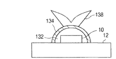
Figure 26 shows a kind of LED structure, and it has the soft interior moulded lens 132 that has interior lens desirable characteristics, the outer lens 136 that serves as boundary layer and be used for the hard middle case 134 of structural stability and be used to produce side emission optical mode.Outer lens 136 can be soft, so that help mould pressing process.Replacedly, can prefabricated outer lens 136 and it is pasted on the middle case 134.The use of middle case 134 makes that the selection of outer lens material is irrelevant with interior lens material basically.
How Figure 27 can make outer lens 138 on any part of interior lens 132 or middle case 134 if showing.
Figure 28 shows directly and make outer lens 142 on interior lens 144 material.
Figure 29 shows the side diversing lens 145 of the another kind of shape of mold pressing on interior lens 132.Can be under without any the situation of interior lens direct moulded lens 145 on LED tube core 10.
Figure 30 shows a kind of LED, and wherein each shell 146,147 comprises different phosphor materials with 148, for example red emission phosphor, green emitted phosphor and blue emission phosphor.LED tube core 10 can be launched UV.Gap between the phosphor particles allows UV to pass inner casing so that the phosphor in shell provides energy.Replacedly, only use red and green phosphor shell, and LED tube core 10 emission blue lights.The combination results white light of redness, green and blue light.In addition, can regulate the thickness of these shells, the density of phosphor particles and the light of order to obtain to wish of phosphor color.Can use the lens of Any shape.
Figure 31 shows 12 of supporting constructions and uses mold pattern 149 on one's body.By this pattern of mold pressing on supporting construction 12, use and the similar method of method shown in Fig. 1, perhaps use metallization process, perhaps use another kind of suitable technology to make high index material (for example polymer) or reflecting material (for example aluminium or silver).Then, mold pattern 149 usefulness are acted on the mould of another material of making lens 150.In one embodiment, lens 150 materials are to be deposited on the liquid (for example silicones) that solidifies then in the mould of making on the supporting construction 12.Then, can be to surface planarization.The lens that obtain collimate this light by the light that reflection/refraction strikes on the wall (such as reflector).
Figure 32 has shown in its side splash metal 151 so that the moulded lens 22 of the light of reflection LED 10 emissions.The light of reflection will and finally be launched by open top by LED 10 scatterings.Metal 151 can be any reflecting material, such as aluminium or silver.This metal can change into splash to the top of lens 22 to form the side emission mode.Lens 22 can be made into Any shape so that form the optical transmission mode of wishing.
Figure 33 is the end view of LCD (LCD) 152, and this LCD has lcd screen 154, diffuser 156 and the backlight 158 that has controlled rgb pixel, and it is used to mix light from red, green and blue led 160 so that produce white light.Backlight 158 is the diffuse reflection case.LED 160 has the side diversing lens that uses above-mentioned any technology to make.
Figure 34 is the end view of back projection TV 162, its have the image in the visual angle that is used for blast regulation front lens 164, one group of redness, green and blue led 166, be used to modulate and focus on rgb light so that the modulator/optics 170 and the reflector 172 of generation colour TV picture.Modulator can be steerable retroreflective lens array, LCD panel or any other suitable device.LED 166 has the collimating lens that uses above-mentioned any technology to make.
As mentioned above, can design main lens or attachment lens to form the side emission mode.This side emission mode mixes light time from a plurality of LED in expection, for example is used to produce at the light from a plurality of LED be used for the even backlight of LED panel or be useful especially when being used for decorative lighting or being used for another purposes.
As shown in figure 35, be not installed to lens on the backboard (backplane) 182 or only have the LED 180 that is installed to the hemispherical lens on the backboard 182 typically will be with lambertian pattern 183 emission light.The back of LED 180 arrays irradiation diffusing screen 184.Screen 184 can be the diffuser 156 in the LCD backlight of Figure 33.Also show diffusion Luminance Distribution 185 and the overall with half high (FWHM) thereof of each LED among the figure.Unless these LED place each other close enough, otherwise the output of the total light of screen 184 fronts will have perceptible speck.Therefore, this backlight needs the LED of relative higher density, thereby causes expensive backlight.
The applicant has invented the wide diversing lens shown in Figure 36-38, and it is particularly useful in backlight.In Figure 36, the LED 188 with wide diversing lens is shown is installed on the backboard 190.The peak light emission (Ipeak) of each LED tube core appears in the 50-80 degree of off-center axle (normal), as shown in figure 37.Scope between the 70-80 degree is preferred.Lens are designed such that along the light emission (I0) of central shaft and are the 5%-33% of peak emission.Correspondingly, the Luminance Distribution 192 of each LED is compared with the Luminance Distribution 185 among Figure 35 more and is launched.Therefore, LED 188 spacings in the backlight of Figure 36 can be bigger than 180 spacings of the LED among Figure 35, realizes identical light output uniformity from diffusing screen 184 simultaneously.This causes so not expensive backlight.
The violent transformation that described Luminance Distribution should not have the funnel-form lens to occur usually at the central tip place.
The optimum ratio of central shaft intensity and 58-80 degree peak strength will depend on application, for example realize the required LED spacing of brightness of the regulation of backlight.Peak strength is three times at least along the intensity of central shaft and in the embodiment of Figure 37, and this ratio is between 4-8.
Figure 38 is the sectional view of an embodiment with wide diversing lens of above-mentioned characteristic.As described in reference Fig. 1-6, LED tube core 194 is installed on the substrate of being made by pottery, silicon or other materials or substrate 196, and as described in reference Fig. 1-6 on LED tube core 194 mold pressing first lens 198.A plurality of tube cores can be installed on the single large substrates.Lens 198 can be made by any suitable material (for example silicones).
Then, separating base plate 196, and attach it on the backboard 190 (PCB) by reflow solder technique or other suitable technology then.
Attachment lens 202 is prefabricated into wide emission characteristics with hope.This attachment lens can be injection moulding or machining plastics or other materials.Such material comprises COC, COP, PMMA, epoxy resin, silicones, glass or any other suitable material.Then, attachment lens 202 is mounted to cover on first lens 198 and contact backboard 190 so that support.Air gap 204 (or other low index of refraction material gap) forms the interior refracting interface that light is bent towards the side.The further crooked light in the outer surface of attachment lens 202 and the interface of air is so that realize the peak strength that the 50-80 degree is interior.Attachment lens 202 can directly contact first lens 198; Yet the shape of attachment lens 202 must be changed so that realize identical wide emission mode.
In another embodiment, attachment lens 202 contact substrates 196 and support rather than contact backboard 190 and support by backboard 190 by substrate 196.
Can utilize the adhesive such as epoxy resin that attachment lens 202 is fixed to backboard or substrate or can utilizes clasp (snap-tab) to be connected and fixed attachment lens 202.
With the reference backboard fixedly attachment lens 202 compare, fix attachment lens 202 by reference substrate and realized a little better control, because the height of the back of the body onboard led and first lens 198 can change a little along with installation parameter.
Non-spherical attachment lens 202 with non-spherical dome inner air crack is the simple designs that are easy to mold pressing.Near lens 202 reverberation that makes progress by undercutting so that at the undercut surface place backboard 190 makes light downwards towards backboard 190 emissions.The light output that this has been avoided the ring of light and has increased backlight.
Figure 39 shows light intensity-angular relationship of the LED of Figure 38.Peak strength about 72 is spent, and is approximately 10% of peak strength along the intensity of central shaft.
In another embodiment, the surface of attachment lens 202 comprises as reference Figure 19, Figure 21 and the described microstructure of Figure 22, the emission mode of its further refract light to realize wishing.
Figure 40 is the sectional view with LED 194 of lens 206, and these lens 206 have total internal reflection (TIR) part 208.This TIR part 208 is a funnel-form.This TIR part 208 make great majority upwards emission light generation internal reflections and by lateral parts 210 emissions.This design can be used to reduce the intensity along central shaft, still provide simultaneously in the 50-80 degree peak strength and along the intensity between the 5-33% of peak strength of central shaft.In the backlight of Figure 33, can adopt any one in these lens embodiment.
Figure 38 and Figure 40 and the attachment lens in other accompanying drawings also can be used on the LED tube core of first lens that do not have mold pressing.Yet preferably first lens with mold pressing use so that protect LED.The diameter of attachment lens typically will be within the scope of 4-10mm.
Figure 41 A-41E showed mold pressing ceramic phosphor plate and will cross the step that moulded board is attached to the LED tube core.Phosphor plate can be made and have accurate characteristic, because can carefully control its thickness (for example 50-300 micron) and phosphor density.When blue light (for example 440nm-460nm) when phosphor provides energy, phosphor is launched more long wavelength's light.When phosphor plate was attached on the blue led, the blue light of certain percentage passed this plate, and this blue light mixes with the light that phosphor produces.
A kind of mode of making the ceramic phosphor sheet is to use the particle of heating and pressure sintering phosphor powder.The percentage that passes the blue LED light of described plate depends on the density of phosphor and the thickness of plate, and it can accurately be controlled.The mode that another kind is made the phosphor thin slice is to make phosphor slurry and dry described slurry then in thin slice.Described in people's such as Gerd Mueller the U.S. Patent application 20050269582 that is entitled as " Luminescent Ceramic for a Light Emitting Diode " and made such ceramic phosphor plate, the document is incorporated herein by reference.
The popular phosphor that uses with blue led is YAG:Ce phosphor (yttrium-aluminium-garnet of about 2% the cerium of having mixed), and it can be in commercial acquisition.
Figure 41 A shows and uses any suitable adhesive to be installed to ceramic phosphor lath sheet 211 on the base plate 212 temporarily, and described adhesive can easily break away from by means of power or by means of solvent.Base plate 212 can have special teflon (Teflon) coating of the silicones that prevents adhesive solidification in step afterwards.Described wafer typically is rectangle, but can have any shape.This wafer will afterwards by sawing so that be formed for the phosphor plate of hundreds of LED.In this example, wafer 211 is the YAG phosphor of 50-300 micron thickness, and it launches greenish-yellow coloured light when being used to from the blue light of blue led and being provided energy.It is dazzling that the white light that obtains is considered to usually, because it has high colour temperature (for example 4000-6000K).As described below, red-emitting phosphor will be used for reducing colour temperature, and this conventionally is being called as the warmer white light of formation.
In Figure 41 B, the impression 213 in mould 214 is filled the liquid silicone resin 215 that comprises red-emitting phosphor particle 216.Conventional sticking mould release film (not shown) is applicator die and allow to remove the silicones of mold pressing afterwards conformally too big pulling force.The automated fluid distributor of any kind can be used for distributing silicones/phosphor blends.The example of red-emitting phosphor comprises known BaSSN, CaS and e-CaS.The shape of the optimum density of red-emitting phosphor particle and impression 213 reduces decision by the colour temperature of the hope that red-emitting phosphor provides.If wish to reach specific colour temperature, also can in silicones 215, use other phosphor particles, for example YAG, green, orange, blue or the like.In one embodiment, employed silicones 215 makes it softer relatively after solidifying, thus during the operation LED structure on LED and the phosphor plate that obtains existence stress seldom.In another embodiment, silicones 215 is identical or equivalent with the silicones that was used to make outer lens afterwards.
Then, base plate 212 and mould 214 are put together, so that phosphor wafer 211 is immersed in the silicones 215.Base plate 212 and mould 214 are clipped together, around structure, form vacuum and silicones 215 is compressed.During this crosses the mold pressing step, emptying any bubble in the liquid silicone resin.Then, by heating or UV solidification of silicon resin 215.Afterwards, by means of mould release film base plate 212 is separated with mould 214.
Then, the mold pressing phosphor wafer that sawing obtains is so that form independent mold pressing phosphor plate, and wherein each plate is similar to the size of LED.Described phosphor loads silicones and form lens on phosphor plate.In one embodiment, during the sawing technology mold pressing phosphor wafer is being retained on the base plate 212, and saw blade is only cut through-wafer.This makes described plate be easier to be picked up by automatic pick and place machine and puts.In another embodiment, remove the mold pressing wafer, carry out sawing then from base plate 212.
In Figure 41 C, automatically picking-placing arms removes each mold pressing phosphor plate 218 (having the YAG plate 220 that phosphor loads silicones 221) and mold pressing phosphor plate 218 is bonded to the end face that is installed in the blue led 224 on the substrate 226 (wafer in this stage) from base plate 212.Substrate 226 can comprise with the similar two-dimensional array of array shown in Fig. 4 in hundreds of blue leds 224.Substrate 226 typically be pottery and comprise the metal trace that is used for each LED and electrode so that be connected to power supply.Phosphor plate 218 can pass through low-melting glass, silicones, epoxy resin, other clear binders or heating with the bonding of LED 224 and pressurization realizes.
In an embodiment that will describe in detail in the back, the shape of mould impression 213 is determined by microcomputer modelling, so that the heterogeneity of the colour temperature-angular relationship of the light of compensation LED/plate combined transmit.
In Figure 41 D, the clear silicone lens 234 of mold pressing on LED 224 and mold pressing phosphor plate 218 is so that the encapsulation total.Technology with reference to Fig. 1-4 and the description of other accompanying drawings can be used for making outer lens 234.Mold pressing outer lens 234 has improved the light extraction of LED, has realized the optical transmission mode of wishing, and has prevented the layering of phosphor plate 218.
In another embodiment, outer lens 234 is harder than phosphor loading silicones 221.This causes the big outer lens of the mechanical strength that is used to protect and the smooth exterior surface face of anti-dust particle, reduces the stress on LED and the interconnection line simultaneously.
Then, cutting substrate 226 is with cutting LED structure.LED in the last example launches for example interior warm white light of 3000-4000K.Any other phosphor may be used to the phosphor in described phosphor plate and the silicones.
Can further control colour temperature by after test, dividing (bin) these mold pressing phosphor plate according to the color characteristics of mold pressing phosphor plate 218.Then, the LED224 on the test base 226 and according to its color characteristics these LED that classify.Then, select the mold pressing phosphor plate 218 of dividing so that realize the target colour temperature for specific LED.
Figure 41 E shows another embodiment that crosses mold pressing phosphor plate 218 that is attached on the LED 224.In Figure 41 E, down mold pressing phosphor plate 218 is attached on the LED 224 by using silicones or heating silicones side.
Except phosphor being cut before the mold pressing, Figure 42 A-42E is similar to Figure 41 A-41E.At first, the sawing or the phosphor sheet that fractures are so that form and the approximately uniform phosphor plate of LED size that energy is provided.
Figure 42 A shows and uses any suitable adhesive to be installed to the two-dimensional array of the ceramic phosphor plate 228 on the base plate 222 temporarily, and described adhesive can easily break away from by means of power or by means of solvent.Base plate 222 and phosphor plate characteristic can with Figure 41 A-41E in identical.
In Figure 42 B, the impression 229 in mould 230 is filled the liquid silicone resin 231 that comprises red-emitting phosphor particle 232.Conventional sticking mould release film (not shown) is applicator die and allow to remove the silicones of mold pressing afterwards conformally too big pulling force.The characteristic of phosphor, silicones and mould and above-described those are similar.
Then, base plate 222 and mould 230 are put together, so that described plate 228 is immersed in the silicones 231.Base plate 222 and mould 230 are clipped together, around structure, form vacuum and silicones 231 is compressed.Then, by heating or UV solidification of silicon resin 231.Afterwards, by means of mould release film base plate 222 is separated with mould 230.
In Figure 42 C, automatically picking-placing arms removes each moulded board 234 and moulded board 234 is bonded to the end face of the blue led 236 that is installed on the substrate wafer 238 from base plate 222.Substrate 238 can comprise with the similar two-dimensional array of array shown in Fig. 4 in hundreds of blue leds 236.Substrate 238 typically be pottery and comprise the metal trace that is used for each LED and electrode so that be connected to power supply.Phosphor plate 228 can pass through low-melting glass, silicones, epoxy resin, other clear binders or heating with the bonding of LED 236 and pressurization realizes.
In an embodiment that will describe in detail in the back, the shape of mould impression 229 is determined by microcomputer modelling, so that the heterogeneity of the colour temperature-angular relationship of the light of compensation LED/plate combined transmit.
In Figure 42 D, the clear silicone lens 244 of mold pressing on LED 236 and moulded board 234 is so that the encapsulation total.Technology with reference to Fig. 1-4 and the description of other accompanying drawings can be used for making outer lens 244.
Then, cutting substrate 238 is with cutting LED structure.LED in the last example launches for example interior warm white light of 3000-4000K.Any other phosphor may be used to the phosphor in described phosphor plate and the silicones.The advantage of dividing and mating is described with reference to Figure 41 A-41E.
Figure 42 E shows another embodiment that crosses mold pressing phosphor plate 234 that is attached on the LED tube core.In Figure 42 E, moulded board 234 is attached on the LED 236 by using silicones or adding under the thermal lens side direction.Let slip journey in order to simplify ten, base plate 222 (Figure 42 B) can break away from from moulded board, and moulded board still is in the mould 230 simultaneously.Then, picking-placing arms is attached to the plate of exposure, removes moulded board and place it on the LED 236 from mould 230.
In Figure 41 A-E and Figure 42 A-E, the first mold pressing step only covers phosphor plate.Figure 43 A-43D shows wherein the also technology of packaged LED of the first mold pressing step.
In Figure 43 A, phosphor plate 228 (for example YAG) is attached on the LED tube core 236 on the substrate 238.
In Figure 43 B, the impression 248 in mould 250 is filled the liquid silicone resin 252 that comprises red-emitting phosphor particle 254.As mentioned above, also can use other phosphor.Substrate 238 and mould 250 are put together, and heating silicones 252 is so that solidify it.For the reason of stating above, the silicones that obtains can be softer relatively, perhaps can be same or similar with the silicones that is used for making outer lens.
In Figure 43 C, substrate 238 is separated with mould 250, make red-emitting phosphor lens 258 encapsulate each LED and phosphor plate, thereby produce warm white light.
In Figure 43 D, use the hard silicone lens 260 of mould pressing process described herein mold pressing on each LED so that encapsulation and protection whole LED structure.As in all embodiments, outer lens 260 can be by the mould setting so that produce optical transmission mode, for example lambertian pattern, side emission mode, collimation pattern or the like in fact arbitrarily.
Figure 44 A-44C shows mould pressing process and is used for producing more uniform colour temperature-visual angle relation.
In Figure 44 A, YAG phosphor 262 powder conformally apply LED 236, obtain smooth phosphor surface.A kind of mode of utilizing phosphor conformally to apply LED is an electrophoretic deposition.Described electrophoretic deposition among people's such as Dave Collins the United States Patent (USP) no.6576488 that is entitled as " Using Electrophoresis to Produce aConformally Coated Phosphor-Converted Light Emitting Semiconductor ", the document is incorporated herein by reference.When phosphor is for example during the plate shown in Figure 43 A, the technology of Figure 44 B and Figure 44 C is suitable equally.The technology of Figure 44 B and Figure 44 C is suitable for equally wherein wishes the more uniform any LED structure of colour temperature-angular relationship.
Colour temperature curve chart shown in Figure 44 A shows that the colour temperature of phosphor coating LED is than the colour temperature under other visual angles cold (higher CCT or more blue) under 0% visual angle.This is because when advancing along surperficial normal direction, and the blue light minimum distance of advancing is passed through phosphor.As a result, when when different angles is watched LED, white light changes color.Although shown reference color temperature is from 3000K to 3500K, these temperature can higher (for example up to 6000K) or are lower, and this depends on the specific phosphors and the thickness of coating.
Accurately be formed in the thickness aspect and change, make that the advance phosphor coating of identical distance by phosphor of blue light is unusual difficulty under all angles.
In order to compensate the heterogeneity of this color-angular relationship, used the moulded lens that comprises equally distributed basically compensation phosphor.In an example, red-emitting phosphor is dispersed in Figure 43 B in mould 250 similar moulds in liquid silicone resin in.The size of mould is determined by microcomputer modelling based on actual colour temperature-angular characteristics of the LED that will proofread and correct.Usually, mould will be protruding, and wherein accurate width, the degree of depth, curvature and phosphor density are determined by microcomputer modelling.LED with phosphor coating places liquid silicone resin, and solidifies this silicones.Then, the LED that will have a moulded lens removes from mould.
Figure 44 B shows an example of the compensation film applanation lens 264 that comprises red-emitting phosphor.Can use other compensation phosphor, this depends on the colour temperature of hope.By the curve chart of colour temperature-angular relationship as can be known, reduced mean temperature by red component from the interpolation of red-emitting phosphor, and the temperature difference (temperature delta) is reduced to 250K from (Figure 44 A's) 500K, thereby obtains more uniform colour temperature-angular relationship.Lens 264 are preferably softer relatively so that the stress on the reduction LED.
In Figure 44 C, use the hard silicone lens 268 of aforementioned techniques mold pressing on color compensating lens 264.
Figure 45 A shows the LED 236 that does not have smooth phosphor layer, and wherein mould is customized shape is improved colour temperature-angular relationship with formation inhomogeneity phosphor loaded lenses 272.Microcomputer modelling is used for LED-based color-angular relationship and determines the optimum shape and the phosphor density of mould.Usually, the shape of lens 272 makes blue light pass the approximately uniform thickness of lens on large-scale angle.The relative size of lens will be than much bigger shown in Figure 45 A.Phosphor in the lens 272 can be the combination of YAG and red or any other phosphor.It is uniform basically that phosphor in the lens distributes.A plurality of overlapping moulded lenses also can be used for realizing the color characteristics of wishing.
Then, the hard outer lens 276 of mold pressing on softer offset lens 272.These lens 276 can be clearly or comprise phosphor.
In Figure 45 B, interior moulded lens 272 comprises the YAG phosphor, and intermediate die applanation lens 277 comprises red-emitting phosphor and hard outer lens 276 does not comprise phosphor. Lens 272 and 277 the two can be formalized so that colour temperature-angular relationship uniformly is provided basically.Also can use the phosphor and the additional phosphor loaded lenses of other types.In some cases, by all phosphor blend not being provided better control in the single lens for color and colour temperature-angular relationship.Outer lens has increased light extraction usually clearly.
Figure 46 A-46D shows at the semiconductor chip of LED tube core and another kind of type (for example Transient Voltage Suppressor (TVS) or photoelectric detector) and goes up moulded lens.
Figure 46 A is the top view of the part of substrate 280, and it illustrates TVS chip 284 and LED 282 between the power supply lead wire that is connected to LED 282.Metal trace on the substrate 280 is not shown.When for example causing voltage surge owing to Electrostatic Discharge, the circuit in the TVS chip 284 is shorted to ground so that bypass LED 282 with transient voltage.Otherwise, may damage LED 282.The TVS circuit is known.According to the knowledge of the applicant, the prior art TVS circuit part that do not have to be used for the lens of LED encapsulates.Substrate 280 shown in Figure 46 A is parts that many wafers to LED and TVS tube core have been installed on it.This substrate wafer will be afterwards by sawing so that the described LED/TVS pairing of cutting.
Figure 46 B is the end view of substrate 280.Has the impression of having filled the liquid silicone resin that comprises phosphor particles with similar mould shown in Figure 43 B and other accompanying drawings.Described substrate wafer and mould are put together, make each LED/TVS pairing be in the silicones in the single impression, and then silicones is solidified.Afterwards, substrate wafer is separated from mould, and obtain the structure of Figure 46 C.Mold pressing phosphor lens 286 has encapsulated this two chips.The shape of the type of the phosphor that uses, the density of phosphor and lens 286 is by the color temperature characteristic decision of hope.In one embodiment, the phosphor in the lens 286 is that the mixture of YAG and red-emitting phosphor is so that produce warm white light when providing energy by blue led 282.
Shown in Figure 46 D, carry out the second mistake mould pressing process similarly so that on mold pressing phosphor lens 286, make silicone lens 288 clearly with the technology shown in previous.As another embodiment, interior lens 286 are preferably soft than outer lens 288.Outer lens 288 is formalized so that the refraction of the hope of light is provided, thereby realizes in fact arbitrarily emission mode and equally intactly encapsulate described chip.The part of outer lens 288 on TVS chip 284 has slight influence to the optical transmission mode of LED.In the embodiment of a reality, the thickness of these two chips is typically with respect to much smaller shown in aspect ratio Figure 46 D of outer lens.For example, the thickness of LED 282 can be 120 microns (its growth substrates is removed), and mold pressing phosphor lens 286 can have 100 microns thickness and outer lens 288 can have 1000 microns on mold pressing phosphor lens 286 thickness on the LED.
The footprint of mold pressing phosphor lens 286 (footprint) needn't be by rounding as the footprint of hemisphere outer lens.The footprint of phosphor lens 286 can be orthoscopic so that just cover this LED and TVS pairing.
As in all embodiments, outer lens can comprise one or more phosphor types so that realize any colour temperature, for example warm white.
Although can be simply on interior silicone lens silicone lens outside the mold pressing, the intermediate plasma of lens is handled the viscosity that has increased between these two lens in having been found that.Plasma treatment a little etching and roughening lens.In making lens stand 200 watts plasma power a few minutes the viscosity between these two silicone lens of (for example 2-15 minute) sufficient to guarantee greater than the viscosity of outer lens to the mould release film of mould.Plasma power can be approximated to be 200-600 watt.Plasma gas can be any suitable inert gas (a for example argon), and can carry out this processing in can producing any suitable chamber of plasma.Figure 43 C shows optional plasma 289 steps.This plasma step can be made therein among two or more any embodiment that cross moulded lens and carry out.Verified, provide clearly that silicone lens has increased optical output power 24% as outer lens, this is lower than the refractive index that phosphor loads silicones owing to its refractive index.
In Figure 46 A-46D, LED can be a random color, for example blueness, cyan, green or the like, and can utilize non-led chip to come a plurality of LED of mold pressing.
Figure 47 A-47C shows the single lens of mold pressing on a plurality of LED of different colours.Figure 47 A is the top view of a part that comprises the substrate 290 of red LED 292, green LED 293 and blue led 294.Metal trace is not shown.This substrate wafer comprises many such groups, and each group produces the white light of the colour temperature with any hope according to the relative brightness level of RGB LED.
The ratio of layout, color and every kind of color is unrestricted.For example, the LED group also can comprise White LED, and perhaps this group can comprise 2-3 red LED individually or with one or more greens and blue led, and perhaps this group can be that 2 White LEDs add amber LED.
In Figure 47 B, mould 296 has has filled liquid silicone resin 298 so that make the impression 297 of single lens on every group of RGB LED on the substrate wafer.Substrate 290 is clamped with respect to mould 296, and silicones is cured.
In Figure 47 C, then substrate wafer is separated with mould 296, thus on the LED group, make moulded lens 300.In one embodiment, lens 300 comprise one or more phosphors.Then, the cutting substrate wafer, perhaps the whole base plate wafer can form led display unit.The LED of any amount and color can be encapsulated by the single moulded lens of crossing.
Figure 48 A-48C shows and is crossing moulded lens on the LED and then collimating lens had been attached on the flat of moulded lens.
In Figure 48 A, substrate wafer 310 has been installed LED 312 arrays thereon.The bottom electrode of each LED tube core is bonded ultrasonically to metal contact pad on the substrate by using Metal Ball 314.Also can use other bonding techniques.Then, substrate wafer 310 is clipped on the mould, wherein each LED is in the previous mould impression of having filled liquid silicone resin.These impressions are the shape of the mold pressing silicone lens 316 shown in Figure 48 A.Thereafter, solidification of silicon resin.Then, substrate wafer 310 is separated from mould.Each moulded lens 316 has encapsulated LED and has had smooth top.
Subsequently, by silicon resin glue 319, epoxy resin or by other means prefabricated Fresnel Lenses 318 is attached on the flat of moulded lens 316.Fresnel Lenses 318 has the very fine feature to optical alignment.Why can not be that mould release film (it is at the layer that forms 50 microns on the mould) can not be according to such fine pattern formation profile in mould by the direct reason that forms Fresnel Lenses in moulded lens 316 of the pattern in the mould.If mould is made by adhesive material not and is not needed release layer, so can be in described lens direct mold pressing Fresnel Lenses.Independent Fresnel Lenses 318 can or use other means to make by the softening plastic material of punching press.In one embodiment, Fresnel Lenses 318 has circular footprint.
The wall part 320 of moulded lens 316 surrounds each Fresnel Lenses 318 and has approximately uniform height with Fresnel Lenses 318.This wall part 320 has angled side, and it upwards reflects any light from Fresnel Lenses 318 side-emitted.In addition, wall part 320 protection Fresnel Lenses 318 are not impacted.Providing wall part to moulded lens is optionally, and moulded lens can be the arbitrary shape at another lens of top braces.
Then, along sawline 322 sawing substrate wafer 310 so that the light source of cutting collimation.In one embodiment, the light source of Figure 48 A-C microflash of the cell phone camera that acts on Figure 16.Can use the collimating lens of other types.
Moulded lens also can comprise phosphor, shown in Figure 48 B.In Figure 48 B, LED launches blue light and when moulded lens 330, dissimilar phosphors 326,328 are distributed in the liquid silicone resin.In one embodiment, these phosphors provide at least red and green composition to blue light so that the generation white light.In one embodiment, these phosphors comprise red-emitting phosphor and the YAG phosphor that is used for warm white light.
Figure 48 C shows and wherein utilizes phosphor 334 (for example YAG) conformally to apply the embodiment of blue led 312.Described coating can be finished by using electrophoresis.Mold pressing silicone lens 336 comprises red-emitting phosphor 338 so that produce warm white light.
Figure 49 A and Figure 49 B show the space below the use silicone gel underfilling filling AlInGaNLED tube core, and wherein LED is then by hard outer lens encapsulation.In Figure 49 A, the LED 340 towards the top is installed on the substrate 342 with its growth substrates (for example sapphire), makes hard contact 344 on the LED 340 be bonded to the metal trace 346 on the substrate 342.These metal trace end at line pad or the mounted on surface pad on substrate 342 bottoms.Then, the underfill material 348 such as silicone gel is expelled under the LED 340 so that fill the space that produces between LED 340 and the substrate 342.Then, solidify described gel.It is softer relatively that the gel of this curing keeps.
Then, the excimer laser bundle is applied on the transparent growth substrates, it heats the GaNLED surface and separates GaN so that produce gallium and nitrogen in this surface.Nitrogen expands so that Sapphire Substrate lifts away from GaN LED, and removes this Sapphire Substrate.During this technology, produced huge downward pressure, and underfilling 348 mechanically supports thin LED layer in case the LED breakage.Underfilling 348 also helps during operation LED heat to be transmitted to substrate from LED.
Then, use technology described herein mold pressing on LED clear or loaded the hard silicone lens 350 of phosphor.Underfilling 348 prevents that the liquid outer lens material in the mould from entering the space.This has reduced the thermal stress on the operating period LED, itself otherwise may cause LED to lift away from substrate.Underfilling can be optimized so that be indifferent to its function of realization under the situation of its optical characteristics.
Figure 49 B shows sapphire growth substrate 354 wherein and is retained in embodiment on the LED layer.Can be along the side of LED 340 and substrate 354 deposition underfilling 356 so as to guarantee that all spaces are filled and when LED during operation is heated and cools off, reduce the LED/ substrate and hard outer moulded lens 358 between pressure.In addition, if underfilling is opaque, stop the side emission along the underfilling of side so, this is positioned under the situation on the substrate top at phosphor layer is favourable.As in all embodiments, outer lens can load phosphor.
In all embodiment described herein, can adopt the underfilling silicone gel.In addition, can replace blue led described herein and use the LED of emission UV light, and blue phosphor can be distributed in the moulded lens.
Although shown and described specific embodiment of the present invention, but for those skilled in the art clearly, can make some changes and modification without departing from the invention aspect wider of the present invention, and therefore claims should comprise all such changes and the modification that falls in true spirit of the present invention and the scope in its scope.
Claims (9)
1. technology that is used to make light-emitting diode (LED) structure comprises:
The LED (236) of emission blue light is provided on substrate (238);
Smooth prefabricated phosphor plate (228) is attached on the LED, and this prefabricated phosphor plate comprises the YAG phosphor of launching sodium yellow, wherein from the blue light that passes through this phosphor plate leakage of this LED and the combination results white light of described sodium yellow;
The mould (250) that has with the corresponding impression (248) of intermediate lens (258) is provided;
Utilization comprises the liquid lens material (252) of phosphor (254) and fills impression, and this phosphor produces red light at least when being encouraged by the blue light that leaks by described phosphor plate;
After filling step, the part of phosphor plate and described LED at least is immersed in the liquid lens material in the mould; And
Solidify liquid lens material, so that on described phosphor plate and LED, make phosphor loaded lenses (258).
2. the technology of claim 1, wherein said liquid lens material (252) encapsulates described LED (236) and phosphor plate (228).
3. the technology of claim 1 also comprises by described phosphor loaded lenses and LED being immersed in the liquid lens material (252) in the mould impression and solidifying this liquid lens material then and comes the clear lens of mold pressing (260) on described phosphor loaded lenses (258) and LED (236).
4. the technology of claim 1 also comprises colour temperature-visual angle relation of determining described phosphor plate (228) subsides LED (236) thereon, and then described mould impression is formalized (264) to increase the uniformity of this colour temperature-visual angle relation.
5. the technology of claim 1 is wherein from the combination results white light of the light of described LED (236), phosphor plate (228) and phosphor loaded lenses (258).
6. the technology of claim 1, wherein described LED (236) is installed on the substrate (238) together with a plurality of identical LED, the step that wherein described at least phosphor plate is immersed in the liquid lens material in the described mould comprises in the liquid lens material that simultaneously all LED on this substrate is immersed in the related mould impression.
7. a light-emitting diode (LED) structure comprises:
Substrate (238) is gone up the LED (236) of emission blue light;
Be attached to the smooth prefabricated phosphor plate (228) on this LED, this prefabricated phosphor plate comprises the YAG phosphor of launching sodium yellow, wherein from the blue light that passes through this phosphor plate leakage of this LED and the combination results white light of described sodium yellow;
The phosphor loaded lenses (258) of the mold pressing on described phosphor plate and LED, it produces red light at least when being encouraged by the blue light that leaks by described phosphor plate; And
The clear lens (260) that do not contain phosphor of mold pressing on described LED and phosphor loaded lenses.
8. the structure of claim 7, wherein the LED (236) that combines with described phosphor plate (228) has certain colour temperature-visual angle relation, and wherein to described phosphor loaded lenses setting (264) so that increase the uniformity of this colour temperature-visual angle relation.
9. the structure of claim 7 is wherein from the combination results white light of the light of described LED (236), phosphor plate (228) and phosphor loaded lenses (258).
Applications Claiming Priority (3)
| Application Number | Priority Date | Filing Date | Title |
|---|---|---|---|
| US11/679,143 US7858408B2 (en) | 2004-11-15 | 2007-02-26 | LED with phosphor tile and overmolded phosphor in lens |
| US11/679,143 | 2007-02-26 | ||
| PCT/IB2008/050692 WO2008104936A2 (en) | 2007-02-26 | 2008-02-26 | Led with phosphor tile and overmolded phosphor in lens |
Publications (2)
| Publication Number | Publication Date |
|---|---|
| CN101636851A CN101636851A (en) | 2010-01-27 |
| CN101636851B true CN101636851B (en) | 2011-12-21 |
Family
ID=39540660
Family Applications (1)
| Application Number | Title | Priority Date | Filing Date |
|---|---|---|---|
| CN2008800062087A Expired - Fee Related CN101636851B (en) | 2007-02-26 | 2008-02-26 | LED structure and process for producing LED structure |
Country Status (7)
| Country | Link |
|---|---|
| US (2) | US7858408B2 (en) |
| EP (1) | EP2115789A2 (en) |
| JP (1) | JP2010519757A (en) |
| KR (1) | KR20090127296A (en) |
| CN (1) | CN101636851B (en) |
| TW (1) | TW200901514A (en) |
| WO (1) | WO2008104936A2 (en) |
Cited By (2)
| Publication number | Priority date | Publication date | Assignee | Title |
|---|---|---|---|---|
| CN105874618A (en) * | 2014-01-08 | 2016-08-17 | 皇家飞利浦有限公司 | Wavelength converted semiconductor light emitting device |
| US9431589B2 (en) | 2007-12-14 | 2016-08-30 | Cree, Inc. | Textured encapsulant surface in LED packages |
Families Citing this family (363)
| Publication number | Priority date | Publication date | Assignee | Title |
|---|---|---|---|---|
| US9142734B2 (en) | 2003-02-26 | 2015-09-22 | Cree, Inc. | Composite white light source and method for fabricating |
| WO2004100279A2 (en) * | 2003-04-30 | 2004-11-18 | Cree, Inc. | High-power solid state light emitter package |
| US7005679B2 (en) * | 2003-05-01 | 2006-02-28 | Cree, Inc. | Multiple component solid state white light |
| US8999736B2 (en) * | 2003-07-04 | 2015-04-07 | Epistar Corporation | Optoelectronic system |
| US20050259418A1 (en) * | 2004-05-18 | 2005-11-24 | Callegari Mark R | Expanded bit map display for mounting on a building surface and a method of creating same |
| US7534633B2 (en) * | 2004-07-02 | 2009-05-19 | Cree, Inc. | LED with substrate modifications for enhanced light extraction and method of making same |
| WO2006029025A2 (en) * | 2004-09-04 | 2006-03-16 | Applied Materials, Inc. | Substrate carrier having reduced height |
| US8134292B2 (en) * | 2004-10-29 | 2012-03-13 | Ledengin, Inc. | Light emitting device with a thermal insulating and refractive index matching material |
| US8324641B2 (en) * | 2007-06-29 | 2012-12-04 | Ledengin, Inc. | Matrix material including an embedded dispersion of beads for a light-emitting device |
| US8816369B2 (en) | 2004-10-29 | 2014-08-26 | Led Engin, Inc. | LED packages with mushroom shaped lenses and methods of manufacturing LED light-emitting devices |
| US9929326B2 (en) | 2004-10-29 | 2018-03-27 | Ledengin, Inc. | LED package having mushroom-shaped lens with volume diffuser |
| ITRM20040633A1 (en) * | 2004-12-23 | 2005-03-23 | St Microelectronics Srl | MULTI-SOURCE OPTICAL TRANSMITTER AND PHOTON DISPLAY DEVICE. |
| US8125137B2 (en) * | 2005-01-10 | 2012-02-28 | Cree, Inc. | Multi-chip light emitting device lamps for providing high-CRI warm white light and light fixtures including the same |
| US7564180B2 (en) | 2005-01-10 | 2009-07-21 | Cree, Inc. | Light emission device and method utilizing multiple emitters and multiple phosphors |
| US7821023B2 (en) * | 2005-01-10 | 2010-10-26 | Cree, Inc. | Solid state lighting component |
| TWI352437B (en) | 2007-08-27 | 2011-11-11 | Epistar Corp | Optoelectronic semiconductor device |
| JP4634810B2 (en) * | 2005-01-20 | 2011-02-16 | 信越化学工業株式会社 | Silicone sealed LED |
| US20070000849A1 (en) * | 2005-01-25 | 2007-01-04 | Daktronics, Inc. | Modular display system |
| US20150295154A1 (en) | 2005-02-03 | 2015-10-15 | Epistar Corporation | Light emitting device and manufacturing method thereof |
| US8163580B2 (en) | 2005-08-10 | 2012-04-24 | Philips Lumileds Lighting Company Llc | Multiple die LED and lens optical system |
| US8172097B2 (en) * | 2005-11-10 | 2012-05-08 | Daktronics, Inc. | LED display module |
| US7907133B2 (en) | 2006-04-13 | 2011-03-15 | Daktronics, Inc. | Pixel interleaving configurations for use in high definition electronic sign displays |
| US8130175B1 (en) | 2007-04-12 | 2012-03-06 | Daktronics, Inc. | Pixel interleaving configurations for use in high definition electronic sign displays |
| KR20090009772A (en) * | 2005-12-22 | 2009-01-23 | 크리 엘이디 라이팅 솔루션즈, 인크. | Lighting device |
| US7777322B2 (en) | 2005-12-30 | 2010-08-17 | Dialight Corporation | Apparatus for providing a light source that combines different color LEDS |
| US7918582B2 (en) * | 2005-12-30 | 2011-04-05 | Dialight Corporation | Signal light using phosphor coated LEDs |
| CN101432895B (en) | 2006-04-24 | 2012-09-05 | 克利公司 | Side-view surface mount white LED |
| EA200870494A1 (en) * | 2006-05-02 | 2009-06-30 | Супербалбс, Инк. | PLASTIC LED LAMP |
| AU2007248756A1 (en) | 2006-05-02 | 2007-11-15 | Carol Lenk | Method of light dispersion and preferential scattering of certain wavelengths of light for light-emitting diodes and bulbs constructed therefrom |
| CA2645231A1 (en) * | 2006-05-02 | 2007-11-15 | Superbulbs, Inc. | Heat removal design for led bulbs |
| DE102007021042A1 (en) | 2006-07-24 | 2008-01-31 | Samsung Electro-Mechanics Co., Ltd., Suwon | Light-emitting diode module for light source series |
| JP2008060542A (en) * | 2006-08-03 | 2008-03-13 | Toyoda Gosei Co Ltd | Light-emitting device, method of manufacturing same, and light source device provided with the same |
| US20080029720A1 (en) | 2006-08-03 | 2008-02-07 | Intematix Corporation | LED lighting arrangement including light emitting phosphor |
| US20100224890A1 (en) * | 2006-09-18 | 2010-09-09 | Cree, Inc. | Light emitting diode chip with electrical insulation element |
| JP4858966B2 (en) * | 2006-11-02 | 2012-01-18 | Towa株式会社 | Electronic component compression molding method and molding apparatus |
| US7889421B2 (en) * | 2006-11-17 | 2011-02-15 | Rensselaer Polytechnic Institute | High-power white LEDs and manufacturing method thereof |
| US20080197369A1 (en) * | 2007-02-20 | 2008-08-21 | Cree, Inc. | Double flip semiconductor device and method for fabrication |
| KR100883075B1 (en) * | 2007-03-02 | 2009-02-10 | 엘지전자 주식회사 | Light Emitting Device |
| TWI326923B (en) * | 2007-03-07 | 2010-07-01 | Lite On Technology Corp | White light emitting diode |
| US7618163B2 (en) * | 2007-04-02 | 2009-11-17 | Ruud Lighting, Inc. | Light-directing LED apparatus |
| DE102007017855A1 (en) * | 2007-04-16 | 2008-10-23 | Osram Opto Semiconductors Gmbh | Method for producing an optoelectronic component and optoelectronic component |
| US7999283B2 (en) * | 2007-06-14 | 2011-08-16 | Cree, Inc. | Encapsulant with scatterer to tailor spatial emission pattern and color uniformity in light emitting diodes |
| US8350788B1 (en) | 2007-07-06 | 2013-01-08 | Daktronics, Inc. | Louver panel for an electronic sign |
| US11114594B2 (en) * | 2007-08-24 | 2021-09-07 | Creeled, Inc. | Light emitting device packages using light scattering particles of different size |
| KR101383357B1 (en) * | 2007-08-27 | 2014-04-10 | 엘지이노텍 주식회사 | Light emitting device package and method of making the same |
| WO2009045438A1 (en) | 2007-10-03 | 2009-04-09 | Superbulbs, Inc. | Glass led light bulbs |
| WO2009054948A1 (en) | 2007-10-24 | 2009-04-30 | Superbulbs, Inc. | Diffuser for led light sources |
| US20090159915A1 (en) * | 2007-12-19 | 2009-06-25 | Shaul Branchevsky | Led insert module and multi-layer lens |
| KR100998009B1 (en) * | 2008-03-12 | 2010-12-03 | 삼성엘이디 주식회사 | Light emitting diode package and method of manufacturing the same |
| JP5665160B2 (en) * | 2008-03-26 | 2015-02-04 | パナソニックIpマネジメント株式会社 | Light emitting device and lighting apparatus |
| DE102008016487A1 (en) * | 2008-03-31 | 2009-10-01 | Osram Opto Semiconductors Gmbh | Optoelectronic semiconductor component and method for producing an optoelectronic semiconductor component |
| US9287469B2 (en) * | 2008-05-02 | 2016-03-15 | Cree, Inc. | Encapsulation for phosphor-converted white light emitting diode |
| US9207385B2 (en) | 2008-05-06 | 2015-12-08 | Qd Vision, Inc. | Lighting systems and devices including same |
| WO2009137053A1 (en) | 2008-05-06 | 2009-11-12 | Qd Vision, Inc. | Optical components, systems including an optical component, and devices |
| WO2009151515A1 (en) | 2008-05-06 | 2009-12-17 | Qd Vision, Inc. | Solid state lighting devices including quantum confined semiconductor nanoparticles |
| DE102008049777A1 (en) * | 2008-05-23 | 2009-11-26 | Osram Opto Semiconductors Gmbh | Optoelectronic module |
| CN102113119A (en) * | 2008-05-29 | 2011-06-29 | 克利公司 | Light source with near field mixing |
| US7868340B2 (en) * | 2008-05-30 | 2011-01-11 | Bridgelux, Inc. | Method and apparatus for generating white light from solid state light emitting devices |
| US8847249B2 (en) | 2008-06-16 | 2014-09-30 | Soraa, Inc. | Solid-state optical device having enhanced indium content in active regions |
| CN101971378A (en) * | 2008-06-23 | 2011-02-09 | 松下电器产业株式会社 | Light-emitting device, surface light-emitting apparatus, display system |
| EP2312658B1 (en) * | 2008-07-03 | 2018-06-27 | Samsung Electronics Co., Ltd. | A wavelength-converting light emitting diode (led) chip and method for fabrication of an led device equipped with this chip |
| US8805134B1 (en) | 2012-02-17 | 2014-08-12 | Soraa Laser Diode, Inc. | Methods and apparatus for photonic integration in non-polar and semi-polar oriented wave-guided optical devices |
| US8143148B1 (en) | 2008-07-14 | 2012-03-27 | Soraa, Inc. | Self-aligned multi-dielectric-layer lift off process for laser diode stripes |
| US8767787B1 (en) | 2008-07-14 | 2014-07-01 | Soraa Laser Diode, Inc. | Integrated laser diodes with quality facets on GaN substrates |
| US8284810B1 (en) | 2008-08-04 | 2012-10-09 | Soraa, Inc. | Solid state laser device using a selected crystal orientation in non-polar or semi-polar GaN containing materials and methods |
| US8124996B2 (en) | 2008-08-04 | 2012-02-28 | Soraa, Inc. | White light devices using non-polar or semipolar gallium containing materials and phosphors |
| EP2329315A4 (en) * | 2008-09-01 | 2012-01-18 | Lensvector Inc | Wafer-level fabrication of liquid crystal optoelectronic devices |
| US8022626B2 (en) * | 2008-09-16 | 2011-09-20 | Osram Sylvania Inc. | Lighting module |
| US8183585B2 (en) | 2008-09-16 | 2012-05-22 | Osram Sylvania Inc. | Lighting module |
| US8188486B2 (en) * | 2008-09-16 | 2012-05-29 | Osram Sylvania Inc. | Optical disk for lighting module |
| US7858409B2 (en) * | 2008-09-18 | 2010-12-28 | Koninklijke Philips Electronics N.V. | White point compensated LEDs for LCD displays |
| US8403538B2 (en) * | 2008-09-30 | 2013-03-26 | Tyco Electronics Corporation | Color homogenizing optical assembly |
| US8534890B2 (en) * | 2008-10-09 | 2013-09-17 | Tyco Electronics Canada Ulc | Light pipe assembly having optical concentrator |
| US8328390B2 (en) * | 2008-10-09 | 2012-12-11 | Phoseon Technology, Inc. | High irradiance through off-center optics |
| US8075165B2 (en) * | 2008-10-14 | 2011-12-13 | Ledengin, Inc. | Total internal reflection lens and mechanical retention and locating device |
| US20100109025A1 (en) * | 2008-11-05 | 2010-05-06 | Koninklijke Philips Electronics N.V. | Over the mold phosphor lens for an led |
| DE102008057140A1 (en) | 2008-11-13 | 2010-05-20 | Osram Opto Semiconductors Gmbh | Optoelectronic component |
| US20100123386A1 (en) * | 2008-11-13 | 2010-05-20 | Maven Optronics Corp. | Phosphor-Coated Light Extraction Structures for Phosphor-Converted Light Emitting Devices |
| RU2508498C2 (en) * | 2008-11-18 | 2014-02-27 | Конинклейке Филипс Электроникс Н.В. | Electric lamp |
| US8507300B2 (en) * | 2008-12-24 | 2013-08-13 | Ledengin, Inc. | Light-emitting diode with light-conversion layer |
| BRPI1005164A2 (en) * | 2009-01-21 | 2019-04-24 | Koninl Philips Electronics Nv | light source and light recycling device |
| US20100181582A1 (en) * | 2009-01-22 | 2010-07-22 | Intematix Corporation | Light emitting devices with phosphor wavelength conversion and methods of manufacture thereof |
| TWI376043B (en) * | 2009-01-23 | 2012-11-01 | Everlight Electronics Co Ltd | Light emitting device package structure and manufacturing method thereof |
| CA2751030A1 (en) | 2009-01-28 | 2010-08-05 | Koninklijke Philips Electronics N.V. | Illumination system with remote phosphor layer and/or scattering layer |
| JP5680278B2 (en) * | 2009-02-13 | 2015-03-04 | シャープ株式会社 | Light emitting device |
| US7828453B2 (en) * | 2009-03-10 | 2010-11-09 | Nepes Led Corporation | Light emitting device and lamp-cover structure containing luminescent material |
| US8247886B1 (en) | 2009-03-09 | 2012-08-21 | Soraa, Inc. | Polarization direction of optical devices using selected spatial configurations |
| JP5327042B2 (en) * | 2009-03-26 | 2013-10-30 | 豊田合成株式会社 | LED lamp manufacturing method |
| US20100244064A1 (en) * | 2009-03-27 | 2010-09-30 | Avago Technologies Ecbu Ip (Singapore) Pte. Ltd. | Light source |
| US8422525B1 (en) | 2009-03-28 | 2013-04-16 | Soraa, Inc. | Optical device structure using miscut GaN substrates for laser applications |
| US7994531B2 (en) * | 2009-04-02 | 2011-08-09 | Visera Technologies Company Limited | White-light light emitting diode chips and fabrication methods thereof |
| US8299473B1 (en) | 2009-04-07 | 2012-10-30 | Soraa, Inc. | Polarized white light devices using non-polar or semipolar gallium containing materials and transparent phosphors |
| US20140175377A1 (en) * | 2009-04-07 | 2014-06-26 | Soraa, Inc. | Polarized white light devices using non-polar or semipolar gallium containing materials and transparent phosphors |
| WO2010120819A1 (en) | 2009-04-13 | 2010-10-21 | Kaai, Inc. | Optical device structure using gan substrates for laser applications |
| US8837545B2 (en) | 2009-04-13 | 2014-09-16 | Soraa Laser Diode, Inc. | Optical device structure using GaN substrates and growth structures for laser applications |
| US8634442B1 (en) | 2009-04-13 | 2014-01-21 | Soraa Laser Diode, Inc. | Optical device structure using GaN substrates for laser applications |
| US8323998B2 (en) * | 2009-05-15 | 2012-12-04 | Achrolux Inc. | Methods and apparatus for forming uniform layers of phosphor material on an LED encapsulation structure |
| US8791499B1 (en) | 2009-05-27 | 2014-07-29 | Soraa, Inc. | GaN containing optical devices and method with ESD stability |
| US8427590B2 (en) | 2009-05-29 | 2013-04-23 | Soraa, Inc. | Laser based display method and system |
| US8247887B1 (en) | 2009-05-29 | 2012-08-21 | Soraa, Inc. | Method and surface morphology of non-polar gallium nitride containing substrates |
| US10108079B2 (en) | 2009-05-29 | 2018-10-23 | Soraa Laser Diode, Inc. | Laser light source for a vehicle |
| US9829780B2 (en) | 2009-05-29 | 2017-11-28 | Soraa Laser Diode, Inc. | Laser light source for a vehicle |
| US9250044B1 (en) | 2009-05-29 | 2016-02-02 | Soraa Laser Diode, Inc. | Gallium and nitrogen containing laser diode dazzling devices and methods of use |
| US8509275B1 (en) | 2009-05-29 | 2013-08-13 | Soraa, Inc. | Gallium nitride based laser dazzling device and method |
| US9800017B1 (en) | 2009-05-29 | 2017-10-24 | Soraa Laser Diode, Inc. | Laser device and method for a vehicle |
| WO2010151600A1 (en) | 2009-06-27 | 2010-12-29 | Michael Tischler | High efficiency leds and led lamps |
| JP5380182B2 (en) * | 2009-07-03 | 2014-01-08 | パナソニック株式会社 | Light emitting device, surface light source, and liquid crystal display device |
| US8431423B2 (en) * | 2009-07-16 | 2013-04-30 | Koninklijke Philips Electronics N.V. | Reflective substrate for LEDS |
| US8803171B2 (en) * | 2009-07-22 | 2014-08-12 | Koninklijke Philips N.V. | Reduced color over angle variation LEDs |
| US20110031516A1 (en) * | 2009-08-07 | 2011-02-10 | Koninklijke Philips Electronics N.V. | Led with silicone layer and laminated remote phosphor layer |
| US9000466B1 (en) | 2010-08-23 | 2015-04-07 | Soraa, Inc. | Methods and devices for light extraction from a group III-nitride volumetric LED using surface and sidewall roughening |
| US20120138998A1 (en) * | 2009-08-27 | 2012-06-07 | Kyocera Corporation | Light-Emitting Device |
| DE102009040148A1 (en) * | 2009-09-04 | 2011-03-10 | Osram Opto Semiconductors Gmbh | Conversion medium body, optoelectronic semiconductor chip and method for producing an optoelectronic semiconductor chip |
| JP5379615B2 (en) * | 2009-09-09 | 2013-12-25 | パナソニック株式会社 | Lighting device |
| JP5936810B2 (en) * | 2009-09-11 | 2016-06-22 | ローム株式会社 | Light emitting device |
| US20110062472A1 (en) * | 2009-09-17 | 2011-03-17 | Koninklijke Philips Electronics N.V. | Wavelength-converted semiconductor light emitting device |
| US8750342B1 (en) | 2011-09-09 | 2014-06-10 | Soraa Laser Diode, Inc. | Laser diodes with scribe structures |
| US8355418B2 (en) | 2009-09-17 | 2013-01-15 | Soraa, Inc. | Growth structures and method for forming laser diodes on {20-21} or off cut gallium and nitrogen containing substrates |
| US9583678B2 (en) | 2009-09-18 | 2017-02-28 | Soraa, Inc. | High-performance LED fabrication |
| US8933644B2 (en) | 2009-09-18 | 2015-01-13 | Soraa, Inc. | LED lamps with improved quality of light |
| US9293644B2 (en) | 2009-09-18 | 2016-03-22 | Soraa, Inc. | Power light emitting diode and method with uniform current density operation |
| KR101368906B1 (en) | 2009-09-18 | 2014-02-28 | 소라, 인코포레이티드 | Power light emitting diode and method with current density operation |
| US8455910B2 (en) * | 2009-09-21 | 2013-06-04 | Walsin Lihwa Corporation | Method of manufacturing light emitting diode packaging lens and light emitting diode package |
| US20110186887A1 (en) * | 2009-09-21 | 2011-08-04 | Soraa, Inc. | Reflection Mode Wavelength Conversion Material for Optical Devices Using Non-Polar or Semipolar Gallium Containing Materials |
| CN102630288B (en) | 2009-09-25 | 2015-09-09 | 科锐公司 | There is the lighting apparatus of low dazzle and high brightness levels uniformity |
| DE102009048401A1 (en) | 2009-10-06 | 2011-04-07 | Osram Opto Semiconductors Gmbh | Method for producing an optoelectronic semiconductor component and optoelectronic semiconductor component |
| JP2011100715A (en) * | 2009-10-09 | 2011-05-19 | Canon Inc | Light emitting device, display device, and imaging device |
| KR100986468B1 (en) * | 2009-11-19 | 2010-10-08 | 엘지이노텍 주식회사 | Lense and light emitting apparatus including the lense |
| KR100986380B1 (en) | 2009-11-20 | 2010-10-08 | 엘지이노텍 주식회사 | Light emitting apparatus |
| US9480133B2 (en) | 2010-01-04 | 2016-10-25 | Cooledge Lighting Inc. | Light-emitting element repair in array-based lighting devices |
| US8653539B2 (en) | 2010-01-04 | 2014-02-18 | Cooledge Lighting, Inc. | Failure mitigation in arrays of light-emitting devices |
| US8740413B1 (en) | 2010-02-03 | 2014-06-03 | Soraa, Inc. | System and method for providing color light sources in proximity to predetermined wavelength conversion structures |
| US8905588B2 (en) * | 2010-02-03 | 2014-12-09 | Sorra, Inc. | System and method for providing color light sources in proximity to predetermined wavelength conversion structures |
| US20110182056A1 (en) * | 2010-06-23 | 2011-07-28 | Soraa, Inc. | Quantum Dot Wavelength Conversion for Optical Devices Using Nonpolar or Semipolar Gallium Containing Materials |
| US10147850B1 (en) | 2010-02-03 | 2018-12-04 | Soraa, Inc. | System and method for providing color light sources in proximity to predetermined wavelength conversion structures |
| CN102157670A (en) * | 2010-02-11 | 2011-08-17 | 亿光电子工业股份有限公司 | Light-emitting device |
| DE102010008605A1 (en) * | 2010-02-19 | 2011-08-25 | OSRAM Opto Semiconductors GmbH, 93055 | Optoelectronic component |
| DE102010002570A1 (en) * | 2010-03-04 | 2011-07-21 | Osram Gesellschaft mit beschränkter Haftung, 81543 | LED-lighting device e.g. infrared LED lighting device, manufacturing method, involves performing selection of optic element such that luminosity and/or coordinate is approximated to value, and placing selected element behind light source |
| US8319247B2 (en) * | 2010-03-25 | 2012-11-27 | Koninklijke Philips Electronics N.V. | Carrier for a light emitting device |
| US9927611B2 (en) | 2010-03-29 | 2018-03-27 | Soraa Laser Diode, Inc. | Wearable laser based display method and system |
| US8329482B2 (en) | 2010-04-30 | 2012-12-11 | Cree, Inc. | White-emitting LED chips and method for making same |
| TWI561770B (en) * | 2010-04-30 | 2016-12-11 | Samsung Electronics Co Ltd | Light emitting device package, light source module, backlight unit, display apparatus, television set, and illumination apparatus |
| US8451876B1 (en) | 2010-05-17 | 2013-05-28 | Soraa, Inc. | Method and system for providing bidirectional light sources with broad spectrum |
| MY169600A (en) * | 2010-05-24 | 2019-04-22 | Dominant Opto Tech Sdn Bhd | Led lighting device with uniform color mixing |
| WO2011158555A1 (en) * | 2010-06-15 | 2011-12-22 | シャープ株式会社 | Lighting device, display device, and television reception device |
| DE112011101580T5 (en) * | 2010-06-17 | 2013-03-14 | Achrolux Inc. | Light-emitting structure and method for producing the same |
| US8293551B2 (en) | 2010-06-18 | 2012-10-23 | Soraa, Inc. | Gallium and nitrogen containing triangular or diamond-shaped configuration for optical devices |
| US9450143B2 (en) | 2010-06-18 | 2016-09-20 | Soraa, Inc. | Gallium and nitrogen containing triangular or diamond-shaped configuration for optical devices |
| JP5437177B2 (en) * | 2010-06-25 | 2014-03-12 | パナソニック株式会社 | Light emitting device |
| WO2012000114A1 (en) | 2010-06-29 | 2012-01-05 | Cooledge Lightning Inc. | Electronic devices with yielding substrates |
| DE102010026344A1 (en) * | 2010-07-07 | 2012-01-12 | Osram Opto Semiconductors Gmbh | led |
| TW201207324A (en) * | 2010-08-13 | 2012-02-16 | Foxsemicon Integrated Tech Inc | Lightening structure of LED light source |
| US9515229B2 (en) | 2010-09-21 | 2016-12-06 | Cree, Inc. | Semiconductor light emitting devices with optical coatings and methods of making same |
| US9546765B2 (en) | 2010-10-05 | 2017-01-17 | Intematix Corporation | Diffuser component having scattering particles |
| TW201215817A (en) * | 2010-10-05 | 2012-04-16 | Advanced Connectek Inc | Complementary color light source device |
| US8455882B2 (en) * | 2010-10-15 | 2013-06-04 | Cree, Inc. | High efficiency LEDs |
| US20130235557A1 (en) * | 2010-10-22 | 2013-09-12 | Osram Gmbh | Led light source and associated structural unit |
| CN104851957B (en) * | 2010-10-27 | 2019-06-11 | 晶元光电股份有限公司 | Light-emitting diode encapsulation structure |
| US9024341B2 (en) * | 2010-10-27 | 2015-05-05 | Taiwan Semiconductor Manufacturing Company, Ltd. | Refractive index tuning of wafer level package LEDs |
| US8816319B1 (en) | 2010-11-05 | 2014-08-26 | Soraa Laser Diode, Inc. | Method of strain engineering and related optical device using a gallium and nitrogen containing active region |
| US9478719B2 (en) | 2010-11-08 | 2016-10-25 | Bridgelux, Inc. | LED-based light source utilizing asymmetric conductors |
| US8455895B2 (en) | 2010-11-08 | 2013-06-04 | Bridgelux, Inc. | LED-based light source utilizing asymmetric conductors |
| US9048170B2 (en) | 2010-11-09 | 2015-06-02 | Soraa Laser Diode, Inc. | Method of fabricating optical devices using laser treatment |
| US8896235B1 (en) | 2010-11-17 | 2014-11-25 | Soraa, Inc. | High temperature LED system using an AC power source |
| EP2458268B1 (en) * | 2010-11-26 | 2016-04-20 | LG Innotek Co., Ltd. | Phosphor plate and lighting device |
| US20120138981A1 (en) * | 2010-12-02 | 2012-06-07 | Chung-Shan Institute of Science and Technology, Armaments, Bureau, Ministry of National Defense | Light-Emitting Diode Apparatus and Method for Making the Same |
| KR101826745B1 (en) | 2010-12-14 | 2018-02-07 | 삼성전자주식회사 | Varifocal lens structure and method of manufacturing the varifocal lens structure, and optical lens module and method of manufacturing the optical lens module |
| JP5733743B2 (en) * | 2010-12-15 | 2015-06-10 | 日東電工株式会社 | Optical semiconductor device |
| DE102011013369A1 (en) * | 2010-12-30 | 2012-07-05 | Osram Opto Semiconductors Gmbh | A method of manufacturing a plurality of semiconductor devices |
| TWI441361B (en) * | 2010-12-31 | 2014-06-11 | Interlight Optotech Corp | Light emitting diode packaging structure and method for fabricating the same |
| US8652860B2 (en) | 2011-01-09 | 2014-02-18 | Bridgelux, Inc. | Packaging photon building blocks having only top side connections in a molded interconnect structure |
| US8354684B2 (en) | 2011-01-09 | 2013-01-15 | Bridgelux, Inc. | Packaging photon building blocks having only top side connections in an interconnect structure |
| KR101199064B1 (en) * | 2011-01-21 | 2012-11-07 | 엘지이노텍 주식회사 | Light conversion member, display device having the same and method of fabricating the same |
| US9025635B2 (en) | 2011-01-24 | 2015-05-05 | Soraa Laser Diode, Inc. | Laser package having multiple emitters configured on a support member |
| US8786053B2 (en) | 2011-01-24 | 2014-07-22 | Soraa, Inc. | Gallium-nitride-on-handle substrate materials and devices and method of manufacture |
| US9595813B2 (en) | 2011-01-24 | 2017-03-14 | Soraa Laser Diode, Inc. | Laser package having multiple emitters configured on a substrate member |
| US9318875B1 (en) | 2011-01-24 | 2016-04-19 | Soraa Laser Diode, Inc. | Color converting element for laser diode |
| JP5772007B2 (en) * | 2011-01-24 | 2015-09-02 | 日亜化学工業株式会社 | Light emitting device and method for manufacturing light emitting device |
| US9093820B1 (en) | 2011-01-25 | 2015-07-28 | Soraa Laser Diode, Inc. | Method and structure for laser devices using optical blocking regions |
| US8754440B2 (en) * | 2011-03-22 | 2014-06-17 | Tsmc Solid State Lighting Ltd. | Light-emitting diode (LED) package systems and methods of making the same |
| JP2012199497A (en) * | 2011-03-23 | 2012-10-18 | Panasonic Corp | Light emitting device |
| US9287684B2 (en) | 2011-04-04 | 2016-03-15 | Soraa Laser Diode, Inc. | Laser package having multiple emitters with color wheel |
| DE202011000856U1 (en) | 2011-04-13 | 2011-08-10 | Flextronics Automotive Gmbh & Co.Kg | Display device for the refrigerator temperature |
| KR20120119350A (en) * | 2011-04-21 | 2012-10-31 | 삼성전자주식회사 | Light emitting device module and method for manufacturing the same |
| US9029887B2 (en) * | 2011-04-22 | 2015-05-12 | Micron Technology, Inc. | Solid state lighting devices having improved color uniformity and associated methods |
| EP2704221A4 (en) * | 2011-04-28 | 2014-10-15 | Asahi Rubber Inc | Semiconductor device with lens and method for manufacturing same |
| DE102011102350A1 (en) * | 2011-05-24 | 2012-11-29 | Osram Opto Semiconductors Gmbh | Optical element, optoelectronic component and method for the production of these |
| GB201109065D0 (en) * | 2011-05-31 | 2011-07-13 | Nanoco Technologies Ltd | Semiconductor nanoparticle-containing materials and light emitting devices incorporating the same |
| US8860056B2 (en) | 2011-12-01 | 2014-10-14 | Tsmc Solid State Lighting Ltd. | Structure and method for LED with phosphor coating |
| KR101850979B1 (en) * | 2011-06-03 | 2018-04-20 | 서울반도체 주식회사 | Apparatus and method for forming an encapsulation of light emitting device |
| US8957430B2 (en) * | 2011-06-15 | 2015-02-17 | Cree, Inc. | Gel underfill layers for light emitting diodes |
| US8525190B2 (en) * | 2011-06-15 | 2013-09-03 | Cree, Inc. | Conformal gel layers for light emitting diodes |
| US9642208B2 (en) * | 2011-06-28 | 2017-05-02 | Cree, Inc. | Variable correlated color temperature luminary constructs |
| US20130026514A1 (en) * | 2011-07-25 | 2013-01-31 | Wei-Ping Lin | Light emitting device |
| DE102011079796B4 (en) | 2011-07-26 | 2015-08-13 | Flextronics Automotive Gmbh & Co.Kg | Method for determining PWM values for LED modules |
| KR101795370B1 (en) | 2011-07-28 | 2017-11-08 | 삼성전자주식회사 | Method of manufacturing light emitting device |
| KR20130014256A (en) * | 2011-07-29 | 2013-02-07 | 엘지이노텍 주식회사 | Light emitting device package and lighting system using the same |
| US20130037931A1 (en) * | 2011-08-08 | 2013-02-14 | Leo M. Higgins, III | Semiconductor package with a heat spreader and method of making |
| US8686431B2 (en) | 2011-08-22 | 2014-04-01 | Soraa, Inc. | Gallium and nitrogen containing trilateral configuration for optical devices |
| US9646827B1 (en) | 2011-08-23 | 2017-05-09 | Soraa, Inc. | Method for smoothing surface of a substrate containing gallium and nitrogen |
| CN103797294A (en) * | 2011-09-09 | 2014-05-14 | 皇家飞利浦有限公司 | Light-emitting arrangement |
| US8591069B2 (en) | 2011-09-21 | 2013-11-26 | Switch Bulb Company, Inc. | LED light bulb with controlled color distribution using quantum dots |
| US8971370B1 (en) | 2011-10-13 | 2015-03-03 | Soraa Laser Diode, Inc. | Laser devices using a semipolar plane |
| DE102011116229A1 (en) | 2011-10-17 | 2013-04-18 | Osram Opto Semiconductors Gmbh | Ceramic conversion element, optoelectronic component with a ceramic conversion element and method for producing a ceramic conversion element |
| JP5744697B2 (en) * | 2011-10-17 | 2015-07-08 | Towa株式会社 | Optoelectronic component and manufacturing method thereof |
| KR101883841B1 (en) * | 2011-10-20 | 2018-08-01 | 엘지이노텍 주식회사 | Light emitting module and head lamp having the same |
| US20130154481A1 (en) * | 2011-10-31 | 2013-06-20 | Densen Cao | Led light source |
| JP2013105973A (en) * | 2011-11-16 | 2013-05-30 | Seiko Epson Corp | Light-emitting device, method for manufacturing the same, and projector |
| US8912025B2 (en) | 2011-11-23 | 2014-12-16 | Soraa, Inc. | Method for manufacture of bright GaN LEDs using a selective removal process |
| CN102437276A (en) | 2011-11-25 | 2012-05-02 | 四川新力光源有限公司 | LED device and manufacturing method thereof |
| US8746923B2 (en) | 2011-12-05 | 2014-06-10 | Cooledge Lighting Inc. | Control of luminous intensity distribution from an array of point light sources |
| KR101288918B1 (en) * | 2011-12-26 | 2013-07-24 | 루미마이크로 주식회사 | Manufacturing method of light emitting device having wavelenth-converting layer and light emitting device produced by the same |
| US20130187540A1 (en) * | 2012-01-24 | 2013-07-25 | Michael A. Tischler | Discrete phosphor chips for light-emitting devices and related methods |
| US9117991B1 (en) | 2012-02-10 | 2015-08-25 | Flextronics Ap, Llc | Use of flexible circuits incorporating a heat spreading layer and the rigidizing specific areas within such a construction by creating stiffening structures within said circuits by either folding, bending, forming or combinations thereof |
| US8803185B2 (en) * | 2012-02-21 | 2014-08-12 | Peiching Ling | Light emitting diode package and method of fabricating the same |
| JP2013214716A (en) * | 2012-03-06 | 2013-10-17 | Nitto Denko Corp | Fluorescent sealing sheet, light emitting diode device, and manufacturing method of light emitting diode device |
| DE102012101892B4 (en) | 2012-03-06 | 2021-05-12 | OSRAM Opto Semiconductors Gesellschaft mit beschränkter Haftung | Wavelength conversion element, light-emitting semiconductor component and display device therewith as well as method for producing a wavelength conversion element |
| EP2823515A4 (en) * | 2012-03-06 | 2015-08-19 | Soraa Inc | Light emitting diodes with low refractive index material layers to reduce light guiding effects |
| US9020003B1 (en) | 2012-03-14 | 2015-04-28 | Soraa Laser Diode, Inc. | Group III-nitride laser diode grown on a semi-polar orientation of gallium and nitrogen containing substrates |
| KR101867304B1 (en) * | 2012-03-15 | 2018-06-15 | 삼성전자주식회사 | Method of fabricating light emitting apparatus |
| US9897284B2 (en) | 2012-03-28 | 2018-02-20 | Ledengin, Inc. | LED-based MR16 replacement lamp |
| KR20150004818A (en) | 2012-03-30 | 2015-01-13 | 코닌클리케 필립스 엔.브이. | Light emitting device with wavelength converting side coat |
| US9343871B1 (en) | 2012-04-05 | 2016-05-17 | Soraa Laser Diode, Inc. | Facet on a gallium and nitrogen containing laser diode |
| US10559939B1 (en) | 2012-04-05 | 2020-02-11 | Soraa Laser Diode, Inc. | Facet on a gallium and nitrogen containing laser diode |
| US9800016B1 (en) | 2012-04-05 | 2017-10-24 | Soraa Laser Diode, Inc. | Facet on a gallium and nitrogen containing laser diode |
| KR20130124632A (en) * | 2012-05-07 | 2013-11-15 | 주식회사 포스코엘이디 | Led illuminating apparatus and method for fabricating wavelength conversion member used for the apparatus |
| AT512865B1 (en) * | 2012-05-09 | 2014-12-15 | Zizala Lichtsysteme Gmbh | Lighting device for a motor vehicle headlight and light module and motor vehicle headlight with lighting device |
| KR20130133573A (en) * | 2012-05-29 | 2013-12-09 | 서울반도체 주식회사 | Led back light unit and led television comprising the same |
| US10145026B2 (en) | 2012-06-04 | 2018-12-04 | Slt Technologies, Inc. | Process for large-scale ammonothermal manufacturing of semipolar gallium nitride boules |
| TWI475664B (en) * | 2012-06-04 | 2015-03-01 | Multichip package structure for generating a symmetrical and uniform light-mixing source | |
| US9231178B2 (en) | 2012-06-07 | 2016-01-05 | Cooledge Lighting, Inc. | Wafer-level flip chip device packages and related methods |
| US20140151731A1 (en) * | 2012-06-15 | 2014-06-05 | Nguyen The Tran | Photon conversion structures, devices for light emitting devices |
| US9366394B2 (en) | 2012-06-27 | 2016-06-14 | Flextronics Ap, Llc | Automotive LED headlight cooling system |
| US20140001496A1 (en) | 2012-06-27 | 2014-01-02 | Flextronics Ap, Llc | Relampable led structure |
| USD737499S1 (en) | 2012-07-13 | 2015-08-25 | Asahi Rubber Inc. | Lens for light-emitting diode |
| WO2014013406A1 (en) * | 2012-07-20 | 2014-01-23 | Koninklijke Philips N.V. | Led with ceramic green phosphor and protected red phosphor layer |
| US8971368B1 (en) | 2012-08-16 | 2015-03-03 | Soraa Laser Diode, Inc. | Laser devices having a gallium and nitrogen containing semipolar surface orientation |
| DE102012216552A1 (en) * | 2012-09-17 | 2014-03-20 | Osram Gmbh | LED lighting device manufacturing method, involves covering LED chip with converter layer, filling matrix material in converter layer, roughening surface of LED chip, and applying adhesion promoter on surface of LED chip |
| US9978904B2 (en) | 2012-10-16 | 2018-05-22 | Soraa, Inc. | Indium gallium nitride light emitting devices |
| US9041019B2 (en) * | 2012-10-25 | 2015-05-26 | Flextronics Ap, Llc | Method of and device for manufacturing LED assembly using liquid molding technologies |
| DE102012222475A1 (en) * | 2012-12-06 | 2014-06-12 | Osram Gmbh | LUMINOUS DIODE SHOWING SEVERAL FLUORESCENT RANGE |
| KR101984897B1 (en) * | 2012-12-10 | 2019-06-03 | 삼성디스플레이 주식회사 | Light emitting diode package and manufacturing method thereof |
| KR101287633B1 (en) * | 2012-12-12 | 2013-07-24 | 유버 주식회사 | Method for manufacturing chip on board type led package |
| US8802471B1 (en) | 2012-12-21 | 2014-08-12 | Soraa, Inc. | Contacts for an n-type gallium and nitrogen substrate for optical devices |
| US9761763B2 (en) | 2012-12-21 | 2017-09-12 | Soraa, Inc. | Dense-luminescent-materials-coated violet LEDs |
| CN103000791B (en) * | 2012-12-24 | 2015-06-24 | 佛山市香港科技大学Led-Fpd工程技术研究开发中心 | Light-emitting diode (LED) packaging structure of dispensing coating long-distance type fluorescent powder and manufacture method |
| US20140185269A1 (en) | 2012-12-28 | 2014-07-03 | Intermatix Corporation | Solid-state lamps utilizing photoluminescence wavelength conversion components |
| US8933478B2 (en) | 2013-02-19 | 2015-01-13 | Cooledge Lighting Inc. | Engineered-phosphor LED packages and related methods |
| US8754435B1 (en) | 2013-02-19 | 2014-06-17 | Cooledge Lighting Inc. | Engineered-phosphor LED package and related methods |
| US9748460B2 (en) | 2013-02-28 | 2017-08-29 | Flextronics Ap, Llc | LED back end assembly and method of manufacturing |
| US9470395B2 (en) | 2013-03-15 | 2016-10-18 | Abl Ip Holding Llc | Optic for a light source |
| US9136441B2 (en) * | 2013-03-15 | 2015-09-15 | Grote Industries, Llc | Flexible lighting device |
| US20140264423A1 (en) * | 2013-03-15 | 2014-09-18 | Grote Industries, Llc | Flexible lighting device including a protective conformal coating |
| CN105121951A (en) | 2013-03-15 | 2015-12-02 | 英特曼帝克司公司 | Photoluminescence wavelength conversion components |
| EP3081365B1 (en) | 2013-05-10 | 2021-02-17 | ABL IP Holding LLC | Method and apparatus for manufacturing silicone optics |
| WO2014184757A1 (en) | 2013-05-15 | 2014-11-20 | Koninklijke Philips N.V. | Light emitting device with an optical element and a reflector |
| CN104241262B (en) | 2013-06-14 | 2020-11-06 | 惠州科锐半导体照明有限公司 | Light emitting device and display device |
| US9166372B1 (en) | 2013-06-28 | 2015-10-20 | Soraa Laser Diode, Inc. | Gallium nitride containing laser device configured on a patterned substrate |
| US8994033B2 (en) | 2013-07-09 | 2015-03-31 | Soraa, Inc. | Contacts for an n-type gallium and nitrogen substrate for optical devices |
| EP3022779B1 (en) * | 2013-07-19 | 2020-03-18 | Lumileds Holding B.V. | Pc led with optical element and without substrate carrier |
| JP6318495B2 (en) * | 2013-08-07 | 2018-05-09 | 日亜化学工業株式会社 | Light emitting device |
| US9410664B2 (en) | 2013-08-29 | 2016-08-09 | Soraa, Inc. | Circadian friendly LED light source |
| US9395067B2 (en) | 2013-10-07 | 2016-07-19 | Flextronics Ap, Llc | Method of and apparatus for enhanced thermal isolation of low-profile LED lighting fixtures |
| US9379525B2 (en) | 2014-02-10 | 2016-06-28 | Soraa Laser Diode, Inc. | Manufacturable laser diode |
| US9520695B2 (en) | 2013-10-18 | 2016-12-13 | Soraa Laser Diode, Inc. | Gallium and nitrogen containing laser device having confinement region |
| US9368939B2 (en) | 2013-10-18 | 2016-06-14 | Soraa Laser Diode, Inc. | Manufacturable laser diode formed on C-plane gallium and nitrogen material |
| US9362715B2 (en) | 2014-02-10 | 2016-06-07 | Soraa Laser Diode, Inc | Method for manufacturing gallium and nitrogen bearing laser devices with improved usage of substrate material |
| US9976710B2 (en) | 2013-10-30 | 2018-05-22 | Lilibrand Llc | Flexible strip lighting apparatus and methods |
| US9419189B1 (en) | 2013-11-04 | 2016-08-16 | Soraa, Inc. | Small LED source with high brightness and high efficiency |
| JP2015106641A (en) * | 2013-11-29 | 2015-06-08 | 日亜化学工業株式会社 | Light emitting device |
| JP2017501580A (en) * | 2013-12-19 | 2017-01-12 | コーニンクレッカ フィリップス エヌ ヴェKoninklijke Philips N.V. | LED module with uniform fluorescent lighting |
| WO2015089535A1 (en) * | 2013-12-20 | 2015-06-25 | Zumtobel Lighting Gmbh | Optical element for a light source |
| TWI589964B (en) * | 2013-12-26 | 2017-07-01 | 鴻海精密工業股份有限公司 | Light emitting device and backlight module |
| TWI580079B (en) * | 2013-12-26 | 2017-04-21 | 新世紀光電股份有限公司 | Light emitting diode package structure and light emitting diode module |
| CN104747973A (en) * | 2013-12-30 | 2015-07-01 | 鸿富锦精密工业(深圳)有限公司 | Light emitting device and backlight module |
| CN104752588A (en) * | 2013-12-31 | 2015-07-01 | 晶能光电(江西)有限公司 | Fluorescent glue coating method for flip chip |
| KR102323289B1 (en) * | 2014-01-07 | 2021-11-08 | 루미리즈 홀딩 비.브이. | Glueless light emitting device with phosphor converter |
| JP2017504215A (en) * | 2014-01-23 | 2017-02-02 | コーニンクレッカ フィリップス エヌ ヴェKoninklijke Philips N.V. | Light emitting device having a self-aligned preform lens |
| US9209596B1 (en) | 2014-02-07 | 2015-12-08 | Soraa Laser Diode, Inc. | Manufacturing a laser diode device from a plurality of gallium and nitrogen containing substrates |
| US9520697B2 (en) | 2014-02-10 | 2016-12-13 | Soraa Laser Diode, Inc. | Manufacturable multi-emitter laser diode |
| US9871350B2 (en) | 2014-02-10 | 2018-01-16 | Soraa Laser Diode, Inc. | Manufacturable RGB laser diode source |
| KR20150122360A (en) * | 2014-04-23 | 2015-11-02 | (주)라이타이저코리아 | Package for Light Emitting Device and Method for Manufacturing thereof |
| US20150325748A1 (en) | 2014-05-07 | 2015-11-12 | Genesis Photonics Inc. | Light emitting device |
| KR101641205B1 (en) * | 2014-05-12 | 2016-07-21 | 주식회사 케이케이디씨 | The manufacturing method for LED light module contained adjustable Emitting angle |
| EP3146263B1 (en) * | 2014-05-21 | 2019-09-25 | Lumileds Holding B.V. | Method of attaching a lens to a led module with high alignment accuracy |
| CN105304796B (en) * | 2014-06-06 | 2018-12-28 | 深圳市光峰光电技术有限公司 | The method and optical wavelength conversion chip and light source of preparation optical wavelength conversion chip |
| US9564736B1 (en) | 2014-06-26 | 2017-02-07 | Soraa Laser Diode, Inc. | Epitaxial growth of p-type cladding regions using nitrogen gas for a gallium and nitrogen containing laser diode |
| TWI641285B (en) | 2014-07-14 | 2018-11-11 | 新世紀光電股份有限公司 | Light emitting module and method for manufacturing light emitting unit |
| WO2016034761A1 (en) * | 2014-09-01 | 2016-03-10 | Ledil Oy | Process and mold for fabricating an optical device, and an optical device |
| US12126143B2 (en) | 2014-11-06 | 2024-10-22 | Kyocera Sld Laser, Inc. | Method of manufacture for an ultraviolet emitting optoelectronic device |
| US9246311B1 (en) | 2014-11-06 | 2016-01-26 | Soraa Laser Diode, Inc. | Method of manufacture for an ultraviolet laser diode |
| CN104465954A (en) * | 2014-12-14 | 2015-03-25 | 励春亚 | COB light source packaging technology |
| JP2018508972A (en) | 2014-12-19 | 2018-03-29 | グロ アーベーGlo Ab | Method for generating a light emitting diode array on a backplane |
| US9653642B1 (en) | 2014-12-23 | 2017-05-16 | Soraa Laser Diode, Inc. | Manufacturable RGB display based on thin film gallium and nitrogen containing light emitting diodes |
| US9666677B1 (en) | 2014-12-23 | 2017-05-30 | Soraa Laser Diode, Inc. | Manufacturable thin film gallium and nitrogen containing devices |
| KR20160087048A (en) * | 2015-01-12 | 2016-07-21 | 삼성전자주식회사 | Light emitting diode package |
| KR102322336B1 (en) * | 2015-02-06 | 2021-11-05 | 쑤저우 레킨 세미컨덕터 컴퍼니 리미티드 | Light emitting device package and lighting apparatus including the package |
| US11306897B2 (en) | 2015-02-09 | 2022-04-19 | Ecosense Lighting Inc. | Lighting systems generating partially-collimated light emissions |
| US10801696B2 (en) | 2015-02-09 | 2020-10-13 | Ecosense Lighting Inc. | Lighting systems generating partially-collimated light emissions |
| US10123603B1 (en) | 2015-03-27 | 2018-11-13 | Multek Technologies Limited | Diffuse fiber optic lighting for luggage |
| US10091887B2 (en) * | 2015-04-02 | 2018-10-02 | Tactotek Oy | Multi-material structure with embedded electronics |
| US10686159B2 (en) * | 2015-06-26 | 2020-06-16 | Universal Display Corporation | OLED devices having improved efficiency |
| US20170012186A1 (en) * | 2015-07-09 | 2017-01-12 | Dun-Hua Cao | Novel white light led packaging structure and process for manufacturing the same |
| JP6680868B2 (en) | 2015-08-17 | 2020-04-15 | インフィニット アースロスコピー インコーポレーテッド, リミテッド | light source |
| US11437774B2 (en) | 2015-08-19 | 2022-09-06 | Kyocera Sld Laser, Inc. | High-luminous flux laser-based white light source |
| US10938182B2 (en) | 2015-08-19 | 2021-03-02 | Soraa Laser Diode, Inc. | Specialized integrated light source using a laser diode |
| US10879673B2 (en) | 2015-08-19 | 2020-12-29 | Soraa Laser Diode, Inc. | Integrated white light source using a laser diode and a phosphor in a surface mount device package |
| US11437775B2 (en) | 2015-08-19 | 2022-09-06 | Kyocera Sld Laser, Inc. | Integrated light source using a laser diode |
| KR20170040437A (en) | 2015-10-02 | 2017-04-13 | 삼성디스플레이 주식회사 | Display device |
| US9787963B2 (en) | 2015-10-08 | 2017-10-10 | Soraa Laser Diode, Inc. | Laser lighting having selective resolution |
| JP6985615B2 (en) * | 2015-12-22 | 2021-12-22 | 日亜化学工業株式会社 | Luminescent device |
| US11047534B2 (en) | 2016-01-28 | 2021-06-29 | EcoSense Lighting, Inc. | Multizone mixing cup illumination system |
| CN109642718B (en) * | 2016-01-28 | 2020-10-16 | 生态照明公司 | Illumination with multi-zone fusion cup |
| WO2017131693A1 (en) | 2016-01-28 | 2017-08-03 | Ecosense Lighting Inc | Compositions for led light conversions |
| US10197226B2 (en) | 2016-01-28 | 2019-02-05 | Ecosense Lighting Inc | Illuminating with a multizone mixing cup |
| DE102017102112A1 (en) * | 2016-02-04 | 2017-08-10 | Epistar Corporation | Light-emitting element and its production method |
| TWI780041B (en) | 2016-02-04 | 2022-10-11 | 晶元光電股份有限公司 | Light-emitting element and the manufacturing method thereof |
| CN111108616B (en) | 2016-03-08 | 2024-03-15 | 科鲁斯公司 | Lighting system with lens assembly |
| TWI657293B (en) | 2016-03-29 | 2019-04-21 | 友達光電股份有限公司 | Backlight module |
| EP3451394B1 (en) * | 2016-04-26 | 2021-01-06 | Citizen Electronics Co., Ltd. | Light-emitting device |
| CN205824929U (en) * | 2016-05-30 | 2016-12-21 | 肇庆市立得电子有限公司 | A kind of refrigerator irradiates fluorescent tube and uses the refrigerator doors of this fluorescent tube |
| US10854796B2 (en) * | 2016-07-08 | 2020-12-01 | Eaton Intelligent Power Limited | LED light system having elastomeric encapsulation |
| CN107689408B (en) | 2016-08-04 | 2020-03-17 | 展晶科技(深圳)有限公司 | Light emitting diode flip chip die and display |
| US10340173B2 (en) * | 2016-10-11 | 2019-07-02 | Micron Technology, Inc. | System for handling semiconductor dies |
| JP6955135B2 (en) * | 2016-10-19 | 2021-10-27 | 日亜化学工業株式会社 | Light emitting device and its manufacturing method |
| DE102016122251A1 (en) * | 2016-11-18 | 2018-05-24 | Infineon Technologies Austria Ag | Method of forming semiconductor devices and semiconductor device |
| US11296057B2 (en) | 2017-01-27 | 2022-04-05 | EcoSense Lighting, Inc. | Lighting systems with high color rendering index and uniform planar illumination |
| MX2019009715A (en) | 2017-02-15 | 2020-01-27 | Infinite Arthroscopy Inc Ltd | Wireless medical imaging system comprising a head unit and a light cable that comprises an integrated light source. |
| US20180328552A1 (en) | 2017-03-09 | 2018-11-15 | Lilibrand Llc | Fixtures and lighting accessories for lighting devices |
| WO2018190449A1 (en) * | 2017-04-13 | 2018-10-18 | (주)라이타이저코리아 | Round chip scale package and manufacturing method therefor |
| KR101885511B1 (en) * | 2017-04-28 | 2018-08-06 | 엑센도 주식회사 | Optic element assembly apparatus |
| US10410997B2 (en) | 2017-05-11 | 2019-09-10 | Cree, Inc. | Tunable integrated optics LED components and methods |
| CZ2017391A3 (en) * | 2017-07-03 | 2019-01-16 | Varroc Lighting Systems, s.r.o. | Lighting apparatus, in particular a signal lamp for motor vehicles |
| EP3545561B1 (en) * | 2017-08-25 | 2022-10-26 | Cree Huizhou Solid State Lighting Company Ltd. | Multiple led light source integrated package |
| US10771155B2 (en) | 2017-09-28 | 2020-09-08 | Soraa Laser Diode, Inc. | Intelligent visible light with a gallium and nitrogen containing laser source |
| US10222474B1 (en) | 2017-12-13 | 2019-03-05 | Soraa Laser Diode, Inc. | Lidar systems including a gallium and nitrogen containing laser light source |
| US10879431B2 (en) * | 2017-12-22 | 2020-12-29 | Lumileds Llc | Wavelength converting layer patterning for LED arrays |
| US10551728B1 (en) | 2018-04-10 | 2020-02-04 | Soraa Laser Diode, Inc. | Structured phosphors for dynamic lighting |
| CN114981592B (en) | 2018-05-01 | 2024-08-09 | 克鲁斯有限公司 | Lighting system and device with central silicone module |
| KR20190133878A (en) | 2018-05-24 | 2019-12-04 | 엘지이노텍 주식회사 | Lighting module and lighting apparatus |
| CN114364913A (en) | 2018-12-17 | 2022-04-15 | 生态照明公司 | Stripe lighting system conforming to AC driving power |
| US11239637B2 (en) | 2018-12-21 | 2022-02-01 | Kyocera Sld Laser, Inc. | Fiber delivered laser induced white light system |
| US11421843B2 (en) | 2018-12-21 | 2022-08-23 | Kyocera Sld Laser, Inc. | Fiber-delivered laser-induced dynamic light system |
| US11884202B2 (en) | 2019-01-18 | 2024-01-30 | Kyocera Sld Laser, Inc. | Laser-based fiber-coupled white light system |
| US12000552B2 (en) | 2019-01-18 | 2024-06-04 | Kyocera Sld Laser, Inc. | Laser-based fiber-coupled white light system for a vehicle |
| US10903623B2 (en) | 2019-05-14 | 2021-01-26 | Soraa Laser Diode, Inc. | Method and structure for manufacturable large area gallium and nitrogen containing substrate |
| US11228158B2 (en) | 2019-05-14 | 2022-01-18 | Kyocera Sld Laser, Inc. | Manufacturable laser diodes on a large area gallium and nitrogen containing substrate |
| JP7022284B2 (en) | 2019-06-17 | 2022-02-18 | 日亜化学工業株式会社 | Manufacturing method of light emitting device |
| CN111081848B (en) * | 2019-12-31 | 2021-02-05 | 广东晶科电子股份有限公司 | Method for manufacturing light-emitting device |
| US20230068911A1 (en) * | 2020-03-11 | 2023-03-02 | Lumileds Llc | Laser Lift-Off Processing System Including Metal Grid |
| CA3172206A1 (en) * | 2020-03-16 | 2021-09-23 | Dengke Cai | Light fixture for indoor grow application and components thereof |
| US11032976B1 (en) | 2020-03-16 | 2021-06-15 | Hgci, Inc. | Light fixture for indoor grow application and components thereof |
| US10962700B1 (en) | 2020-03-18 | 2021-03-30 | Ideal Industries Lighting Llc | Field-reconfigurable luminaire |
| USD938584S1 (en) | 2020-03-30 | 2021-12-14 | Lazurite Holdings Llc | Hand piece |
| KR20210155956A (en) * | 2020-06-17 | 2021-12-24 | 엘지이노텍 주식회사 | Light source device and camera test device using the light source device |
| CN113921681A (en) * | 2020-07-10 | 2022-01-11 | 广州市鸿利显示电子有限公司 | Mini LED pressing die, preparation method and Mini LED assembly |
| USD972176S1 (en) | 2020-08-06 | 2022-12-06 | Lazurite Holdings Llc | Light source |
| US12111512B2 (en) | 2020-12-15 | 2024-10-08 | Plx, Inc. | Mount for an optical structure and method of mounting the optical structure to the mount |
| CN113238409A (en) * | 2021-05-27 | 2021-08-10 | 业成科技(成都)有限公司 | Light source structure, backlight module and display device |
| KR20230014508A (en) | 2021-07-21 | 2023-01-30 | 삼성전자주식회사 | Display apparatus and method of manufacturing the same |
| CN113671751B (en) * | 2021-08-18 | 2024-05-14 | 安徽芯瑞达科技股份有限公司 | Near zero OD backlight module |
| KR102607878B1 (en) * | 2021-09-17 | 2023-11-30 | 현대모비스 주식회사 | Led module and car including the same |
| CN117153995A (en) * | 2023-10-30 | 2023-12-01 | 罗化芯显示科技开发(江苏)有限公司 | LED packaging film layer and LED packaging structure |
Citations (1)
| Publication number | Priority date | Publication date | Assignee | Title |
|---|---|---|---|---|
| CN1510766A (en) * | 2002-12-24 | 2004-07-07 | 斯坦雷电气株式会社 | Surface installation white light emitting diodes |
Family Cites Families (39)
| Publication number | Priority date | Publication date | Assignee | Title |
|---|---|---|---|---|
| GB2252746B (en) | 1991-01-17 | 1995-07-12 | Towa Corp | A method of molding resin to seal an electronic part on a lead frame and apparatus therefor |
| JP2900000B2 (en) | 1991-07-12 | 1999-06-02 | タキロン株式会社 | Light emitting display and method of manufacturing the same |
| JP2524955B2 (en) | 1993-04-22 | 1996-08-14 | トーワ株式会社 | Method and apparatus for resin sealing molding of electronic parts |
| JP3423766B2 (en) | 1994-03-11 | 2003-07-07 | Towa株式会社 | Resin encapsulation molding method and mold device for electronic components |
| US6274890B1 (en) | 1997-01-15 | 2001-08-14 | Kabushiki Kaisha Toshiba | Semiconductor light emitting device and its manufacturing method |
| US6525386B1 (en) * | 1998-03-10 | 2003-02-25 | Masimo Corporation | Non-protruding optoelectronic lens |
| US6194742B1 (en) | 1998-06-05 | 2001-02-27 | Lumileds Lighting, U.S., Llc | Strain engineered and impurity controlled III-V nitride semiconductor films and optoelectronic devices |
| US6274924B1 (en) | 1998-11-05 | 2001-08-14 | Lumileds Lighting, U.S. Llc | Surface mountable LED package |
| US6521916B2 (en) | 1999-03-15 | 2003-02-18 | Gentex Corporation | Radiation emitter device having an encapsulant with different zones of thermal conductivity |
| DE19925733C2 (en) * | 1999-06-07 | 2001-07-19 | Montan Tech Gmbh | Arrangement for measuring displacements in the mountains |
| US6133589A (en) | 1999-06-08 | 2000-10-17 | Lumileds Lighting, U.S., Llc | AlGaInN-based LED having thick epitaxial layer for improved light extraction |
| JP2001127346A (en) * | 1999-10-22 | 2001-05-11 | Stanley Electric Co Ltd | Light emitting diode |
| AT410600B (en) * | 1999-12-02 | 2003-06-25 | Hoffmann La Roche | MEASURING CHAMBER WITH LUMINESCENCE OPTICAL SENSOR ELEMENTS |
| JP3073769U (en) * | 2000-06-02 | 2000-12-08 | 株式会社ジェイ・ボックス | Coin cleaning and polishing equipment |
| JP4239439B2 (en) | 2000-07-06 | 2009-03-18 | セイコーエプソン株式会社 | OPTICAL DEVICE, ITS MANUFACTURING METHOD, AND OPTICAL TRANSMISSION DEVICE |
| JP3614776B2 (en) | 2000-12-19 | 2005-01-26 | シャープ株式会社 | Chip component type LED and its manufacturing method |
| US6987613B2 (en) | 2001-03-30 | 2006-01-17 | Lumileds Lighting U.S., Llc | Forming an optical element on the surface of a light emitting device for improved light extraction |
| US6576488B2 (en) | 2001-06-11 | 2003-06-10 | Lumileds Lighting U.S., Llc | Using electrophoresis to produce a conformally coated phosphor-converted light emitting semiconductor |
| US6734465B1 (en) * | 2001-11-19 | 2004-05-11 | Nanocrystals Technology Lp | Nanocrystalline based phosphors and photonic structures for solid state lighting |
| WO2003098711A1 (en) * | 2002-05-17 | 2003-11-27 | Ccs Inc. | Light emitting diode and method for fabricating the same |
| JP4268389B2 (en) | 2002-09-06 | 2009-05-27 | Towa株式会社 | Resin sealing molding method and apparatus for electronic parts |
| US6682331B1 (en) * | 2002-09-20 | 2004-01-27 | Agilent Technologies, Inc. | Molding apparatus for molding light emitting diode lamps |
| US20040070990A1 (en) * | 2002-10-01 | 2004-04-15 | Witold Szypszak | LED illuminator and method of manufacture |
| WO2004100279A2 (en) | 2003-04-30 | 2004-11-18 | Cree, Inc. | High-power solid state light emitter package |
| US7329029B2 (en) | 2003-05-13 | 2008-02-12 | Light Prescriptions Innovators, Llc | Optical device for LED-based lamp |
| WO2005012952A2 (en) | 2003-07-29 | 2005-02-10 | Light Prescriptions Innovators, Llc | Circumferentially emitting luminaires and lens elements formed by transverse-axis profile-sweeps |
| US7029935B2 (en) * | 2003-09-09 | 2006-04-18 | Cree, Inc. | Transmissive optical elements including transparent plastic shell having a phosphor dispersed therein, and methods of fabricating same |
| KR100540848B1 (en) | 2004-01-02 | 2006-01-11 | 주식회사 메디아나전자 | White LED device comprising dual-mold and manufacturing method for the same |
| JP4306508B2 (en) * | 2004-03-29 | 2009-08-05 | 三菱電機株式会社 | Avalanche photodiode |
| US7868343B2 (en) | 2004-04-06 | 2011-01-11 | Cree, Inc. | Light-emitting devices having multiple encapsulation layers with at least one of the encapsulation layers including nanoparticles and methods of forming the same |
| US7361938B2 (en) | 2004-06-03 | 2008-04-22 | Philips Lumileds Lighting Company Llc | Luminescent ceramic for a light emitting device |
| US7553683B2 (en) * | 2004-06-09 | 2009-06-30 | Philips Lumiled Lighting Co., Llc | Method of forming pre-fabricated wavelength converting elements for semiconductor light emitting devices |
| CN101032034A (en) | 2004-06-30 | 2007-09-05 | 克里公司 | Chip-scale methods for packaging light emitting devices and chip-scale packaged light emitting devices |
| US20060091418A1 (en) | 2004-11-04 | 2006-05-04 | Chew Tong F | Side emitting LED device and method of fabrication |
| US7452737B2 (en) | 2004-11-15 | 2008-11-18 | Philips Lumileds Lighting Company, Llc | Molded lens over LED die |
| US7344902B2 (en) | 2004-11-15 | 2008-03-18 | Philips Lumileds Lighting Company, Llc | Overmolded lens over LED die |
| US7352011B2 (en) | 2004-11-15 | 2008-04-01 | Philips Lumileds Lighting Company, Llc | Wide emitting lens for LED useful for backlighting |
| JP4453553B2 (en) * | 2005-01-14 | 2010-04-21 | パナソニック電工株式会社 | Light source device and illumination device |
| JP2007049114A (en) | 2005-05-30 | 2007-02-22 | Sharp Corp | Light emitting device and method of manufacturing the same |
-
2007
- 2007-02-26 US US11/679,143 patent/US7858408B2/en not_active Expired - Fee Related
-
2008
- 2008-02-26 CN CN2008800062087A patent/CN101636851B/en not_active Expired - Fee Related
- 2008-02-26 EP EP08719476A patent/EP2115789A2/en not_active Withdrawn
- 2008-02-26 JP JP2009550363A patent/JP2010519757A/en active Pending
- 2008-02-26 TW TW097106719A patent/TW200901514A/en unknown
- 2008-02-26 KR KR1020097020177A patent/KR20090127296A/en not_active Application Discontinuation
- 2008-02-26 WO PCT/IB2008/050692 patent/WO2008104936A2/en active Application Filing
-
2010
- 2010-11-15 US US12/945,962 patent/US20110057205A1/en not_active Abandoned
Patent Citations (1)
| Publication number | Priority date | Publication date | Assignee | Title |
|---|---|---|---|---|
| CN1510766A (en) * | 2002-12-24 | 2004-07-07 | 斯坦雷电气株式会社 | Surface installation white light emitting diodes |
Cited By (2)
| Publication number | Priority date | Publication date | Assignee | Title |
|---|---|---|---|---|
| US9431589B2 (en) | 2007-12-14 | 2016-08-30 | Cree, Inc. | Textured encapsulant surface in LED packages |
| CN105874618A (en) * | 2014-01-08 | 2016-08-17 | 皇家飞利浦有限公司 | Wavelength converted semiconductor light emitting device |
Also Published As
| Publication number | Publication date |
|---|---|
| US20080048200A1 (en) | 2008-02-28 |
| EP2115789A2 (en) | 2009-11-11 |
| JP2010519757A (en) | 2010-06-03 |
| WO2008104936A3 (en) | 2008-12-04 |
| US20110057205A1 (en) | 2011-03-10 |
| TW200901514A (en) | 2009-01-01 |
| US7858408B2 (en) | 2010-12-28 |
| KR20090127296A (en) | 2009-12-10 |
| CN101636851A (en) | 2010-01-27 |
| WO2008104936A2 (en) | 2008-09-04 |
Similar Documents
| Publication | Publication Date | Title |
|---|---|---|
| CN101636851B (en) | LED structure and process for producing LED structure | |
| TWI393841B (en) | Wide emitting lens for led useful for backlighting | |
| US7344902B2 (en) | Overmolded lens over LED die | |
| US7452737B2 (en) | Molded lens over LED die | |
| EP1922767B1 (en) | Color converted light emitting diode | |
| KR102071463B1 (en) | Led with high thermal conductivity particles in phosphor conversion layer and the method of fabricating the same | |
| US20100109025A1 (en) | Over the mold phosphor lens for an led | |
| US20080121911A1 (en) | Optical preforms for solid state light emitting dice, and methods and systems for fabricating and assembling same | |
| KR102091534B1 (en) | Chip scale packaging light emitting device and manufacturing method of the same |
Legal Events
| Date | Code | Title | Description |
|---|---|---|---|
| C06 | Publication | ||
| PB01 | Publication | ||
| C10 | Entry into substantive examination | ||
| SE01 | Entry into force of request for substantive examination | ||
| C14 | Grant of patent or utility model | ||
| GR01 | Patent grant | ||
| C17 | Cessation of patent right | ||
| CF01 | Termination of patent right due to non-payment of annual fee |
Granted publication date: 20111221 Termination date: 20130226 |