SlideShare a Scribd company logo
VLSI Design Flow
Dr. D. V. Kamath
Professor, Department of E&C Engg.,
Manipal Institute of Technology, Manipal
1
2
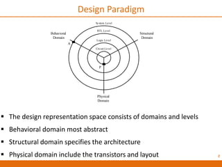
Design Paradigm
Behavioral
Domain
Structural
Domain
Physical
Domain
RTL Level
Logic Level
Circuit Level
System Level
A
P
 The design representation space consists of domains and levels
 Behavioral domain most abstract
 Structural domain specifies the architecture
 Physical domain include the transistors and layout
3
Design Paradigm
Table showing Domains and Level of Design
Domains
Behavioral Structural Physical
Levels
System System
Specifications
Blocks Chip
RTL RTL
Specifications
Registers Macro Cells
Logic Boolean
Functions
Logic Gates Standard
Cells
Circuit Differential
Equations
Transistors Masks
4
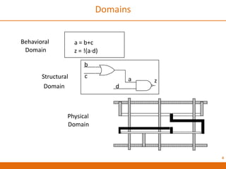
Domains
a = b+c
z = !(a·d)
Behavioral
Domain
Structural
Domain
Physical
Domain
b
c
d
a z
5
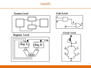
Levels
Register Level
System Level Gate Level
Z
A
B D
C
A
H
Q1
Q8
ENB
Register
A
H
Q1
Q8
ENB
Register
Reg. BReg. A
Adder
Clk
Circuit Level
c
b
d
a
z
6
Typical VLSI Design Flow
7
Front-end design (Logical design) consists of following steps
1. Design entry – Enter the design in to an ASIC design system
using a hardware description language ( HDL ) or schematic entry
2. Logic synthesis – Generation of netlist (logic cells and their
connections) from HDL code. Logic synthesis consists of
following steps :
(i) Technology independent Logic optimization
(ii) Translation: Converting Behavioral description to structural
domain
(iii) Technology mapping or Library binding
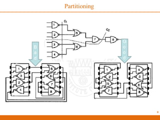
3. System partitioning - Divide a large system into ASIC-sized
pieces
4. Pre-layout simulation - Check to see if the design functions
correctly. Gate level functionality and timing details can be
verified.
Typical VLSI Design Flow
8
Partitioning
9
Back-end design (Physical design) consists of following steps
5. Floor planning - Arrange the blocks of the netlist on the chip
6. Placement - Decide the locations of cells in a block
7. Routing - Make the connections between cells and blocks
8. Circuit Extraction - Determine the resistance and capacitance of
the interconnect
9. Post-layout simulation - Check to see the design still works with
the added loads of the interconnect
Typical VLSI Design Flow
10
Floor planning
 The entire arrangement of blocks, including their positions,
is called a floor-plan
 Every functional module is assigned an outline area so as
to facilitate the gate placement
 Allocation of different pins (I/O, CLK, and other control
pins) of various functional blocks so that internal and
external nets can be routed
11
Placement and Routing
 After partitioning the circuit into smaller modules and floor
planning the layout to determine block outlines and pin
locations, placement determines the locations of standard
cells or logic elements within each block.
 In routing phase, connection between different blocks is
defined.
12
• reachdvkamath@yahoo.com
• dv.kamath@manipal.edu
Contact

More Related Content

vlsi design flow

  • 1. VLSI Design Flow Dr. D. V. Kamath Professor, Department of E&C Engg., Manipal Institute of Technology, Manipal 1
  • 2. 2 Design Paradigm Behavioral Domain Structural Domain Physical Domain RTL Level Logic Level Circuit Level System Level A P  The design representation space consists of domains and levels  Behavioral domain most abstract  Structural domain specifies the architecture  Physical domain include the transistors and layout
  • 3. 3 Design Paradigm Table showing Domains and Level of Design Domains Behavioral Structural Physical Levels System System Specifications Blocks Chip RTL RTL Specifications Registers Macro Cells Logic Boolean Functions Logic Gates Standard Cells Circuit Differential Equations Transistors Masks
  • 4. 4 Domains a = b+c z = !(a·d) Behavioral Domain Structural Domain Physical Domain b c d a z
  • 5. 5 Levels Register Level System Level Gate Level Z A B D C A H Q1 Q8 ENB Register A H Q1 Q8 ENB Register Reg. BReg. A Adder Clk Circuit Level c b d a z
  • 7. 7 Front-end design (Logical design) consists of following steps 1. Design entry – Enter the design in to an ASIC design system using a hardware description language ( HDL ) or schematic entry 2. Logic synthesis – Generation of netlist (logic cells and their connections) from HDL code. Logic synthesis consists of following steps : (i) Technology independent Logic optimization (ii) Translation: Converting Behavioral description to structural domain (iii) Technology mapping or Library binding 3. System partitioning - Divide a large system into ASIC-sized pieces 4. Pre-layout simulation - Check to see if the design functions correctly. Gate level functionality and timing details can be verified. Typical VLSI Design Flow
  • 9. 9 Back-end design (Physical design) consists of following steps 5. Floor planning - Arrange the blocks of the netlist on the chip 6. Placement - Decide the locations of cells in a block 7. Routing - Make the connections between cells and blocks 8. Circuit Extraction - Determine the resistance and capacitance of the interconnect 9. Post-layout simulation - Check to see the design still works with the added loads of the interconnect Typical VLSI Design Flow
  • 10. 10 Floor planning  The entire arrangement of blocks, including their positions, is called a floor-plan  Every functional module is assigned an outline area so as to facilitate the gate placement  Allocation of different pins (I/O, CLK, and other control pins) of various functional blocks so that internal and external nets can be routed
  • 11. 11 Placement and Routing  After partitioning the circuit into smaller modules and floor planning the layout to determine block outlines and pin locations, placement determines the locations of standard cells or logic elements within each block.  In routing phase, connection between different blocks is defined.